EP3193439A1 - Electronic circuit and electronic circuit control method - Google Patents
Electronic circuit and electronic circuit control method Download PDFInfo
- Publication number
- EP3193439A1 EP3193439A1 EP15839562.4A EP15839562A EP3193439A1 EP 3193439 A1 EP3193439 A1 EP 3193439A1 EP 15839562 A EP15839562 A EP 15839562A EP 3193439 A1 EP3193439 A1 EP 3193439A1
- Authority
- EP
- European Patent Office
- Prior art keywords
- circuit
- period
- loss
- power supply
- switching element
- Prior art date
- Legal status (The legal status is an assumption and is not a legal conclusion. Google has not performed a legal analysis and makes no representation as to the accuracy of the status listed.)
- Withdrawn
Links
- 238000000034 method Methods 0.000 title claims description 11
- 239000003990 capacitor Substances 0.000 claims description 25
- 238000009499 grossing Methods 0.000 description 11
- 238000004088 simulation Methods 0.000 description 8
- 230000003071 parasitic effect Effects 0.000 description 3
- 238000001514 detection method Methods 0.000 description 2
- 238000010586 diagram Methods 0.000 description 2
- 230000000694 effects Effects 0.000 description 2
- RYGMFSIKBFXOCR-UHFFFAOYSA-N Copper Chemical compound [Cu] RYGMFSIKBFXOCR-UHFFFAOYSA-N 0.000 description 1
- 238000012986 modification Methods 0.000 description 1
- 230000004048 modification Effects 0.000 description 1
Images



Classifications
-
- H—ELECTRICITY
- H02—GENERATION; CONVERSION OR DISTRIBUTION OF ELECTRIC POWER
- H02M—APPARATUS FOR CONVERSION BETWEEN AC AND AC, BETWEEN AC AND DC, OR BETWEEN DC AND DC, AND FOR USE WITH MAINS OR SIMILAR POWER SUPPLY SYSTEMS; CONVERSION OF DC OR AC INPUT POWER INTO SURGE OUTPUT POWER; CONTROL OR REGULATION THEREOF
- H02M1/00—Details of apparatus for conversion
- H02M1/32—Means for protecting converters other than automatic disconnection
- H02M1/34—Snubber circuits
-
- H—ELECTRICITY
- H02—GENERATION; CONVERSION OR DISTRIBUTION OF ELECTRIC POWER
- H02M—APPARATUS FOR CONVERSION BETWEEN AC AND AC, BETWEEN AC AND DC, OR BETWEEN DC AND DC, AND FOR USE WITH MAINS OR SIMILAR POWER SUPPLY SYSTEMS; CONVERSION OF DC OR AC INPUT POWER INTO SURGE OUTPUT POWER; CONTROL OR REGULATION THEREOF
- H02M1/00—Details of apparatus for conversion
- H02M1/08—Circuits specially adapted for the generation of control voltages for semiconductor devices incorporated in static converters
-
- H—ELECTRICITY
- H02—GENERATION; CONVERSION OR DISTRIBUTION OF ELECTRIC POWER
- H02M—APPARATUS FOR CONVERSION BETWEEN AC AND AC, BETWEEN AC AND DC, OR BETWEEN DC AND DC, AND FOR USE WITH MAINS OR SIMILAR POWER SUPPLY SYSTEMS; CONVERSION OF DC OR AC INPUT POWER INTO SURGE OUTPUT POWER; CONTROL OR REGULATION THEREOF
- H02M1/00—Details of apparatus for conversion
- H02M1/42—Circuits or arrangements for compensating for or adjusting power factor in converters or inverters
- H02M1/4208—Arrangements for improving power factor of AC input
-
- H—ELECTRICITY
- H02—GENERATION; CONVERSION OR DISTRIBUTION OF ELECTRIC POWER
- H02M—APPARATUS FOR CONVERSION BETWEEN AC AND AC, BETWEEN AC AND DC, OR BETWEEN DC AND DC, AND FOR USE WITH MAINS OR SIMILAR POWER SUPPLY SYSTEMS; CONVERSION OF DC OR AC INPUT POWER INTO SURGE OUTPUT POWER; CONTROL OR REGULATION THEREOF
- H02M1/00—Details of apparatus for conversion
- H02M1/42—Circuits or arrangements for compensating for or adjusting power factor in converters or inverters
- H02M1/4208—Arrangements for improving power factor of AC input
- H02M1/4225—Arrangements for improving power factor of AC input using a non-isolated boost converter
-
- H—ELECTRICITY
- H02—GENERATION; CONVERSION OR DISTRIBUTION OF ELECTRIC POWER
- H02M—APPARATUS FOR CONVERSION BETWEEN AC AND AC, BETWEEN AC AND DC, OR BETWEEN DC AND DC, AND FOR USE WITH MAINS OR SIMILAR POWER SUPPLY SYSTEMS; CONVERSION OF DC OR AC INPUT POWER INTO SURGE OUTPUT POWER; CONTROL OR REGULATION THEREOF
- H02M7/00—Conversion of AC power input into DC power output; Conversion of DC power input into AC power output
- H02M7/02—Conversion of AC power input into DC power output without possibility of reversal
- H02M7/04—Conversion of AC power input into DC power output without possibility of reversal by static converters
- H02M7/06—Conversion of AC power input into DC power output without possibility of reversal by static converters using discharge tubes without control electrode or semiconductor devices without control electrode
-
- H—ELECTRICITY
- H02—GENERATION; CONVERSION OR DISTRIBUTION OF ELECTRIC POWER
- H02M—APPARATUS FOR CONVERSION BETWEEN AC AND AC, BETWEEN AC AND DC, OR BETWEEN DC AND DC, AND FOR USE WITH MAINS OR SIMILAR POWER SUPPLY SYSTEMS; CONVERSION OF DC OR AC INPUT POWER INTO SURGE OUTPUT POWER; CONTROL OR REGULATION THEREOF
- H02M1/00—Details of apparatus for conversion
- H02M1/0048—Circuits or arrangements for reducing losses
- H02M1/0054—Transistor switching losses
-
- H—ELECTRICITY
- H02—GENERATION; CONVERSION OR DISTRIBUTION OF ELECTRIC POWER
- H02M—APPARATUS FOR CONVERSION BETWEEN AC AND AC, BETWEEN AC AND DC, OR BETWEEN DC AND DC, AND FOR USE WITH MAINS OR SIMILAR POWER SUPPLY SYSTEMS; CONVERSION OF DC OR AC INPUT POWER INTO SURGE OUTPUT POWER; CONTROL OR REGULATION THEREOF
- H02M1/00—Details of apparatus for conversion
- H02M1/32—Means for protecting converters other than automatic disconnection
- H02M1/34—Snubber circuits
- H02M1/342—Active non-dissipative snubbers
-
- Y—GENERAL TAGGING OF NEW TECHNOLOGICAL DEVELOPMENTS; GENERAL TAGGING OF CROSS-SECTIONAL TECHNOLOGIES SPANNING OVER SEVERAL SECTIONS OF THE IPC; TECHNICAL SUBJECTS COVERED BY FORMER USPC CROSS-REFERENCE ART COLLECTIONS [XRACs] AND DIGESTS
- Y02—TECHNOLOGIES OR APPLICATIONS FOR MITIGATION OR ADAPTATION AGAINST CLIMATE CHANGE
- Y02B—CLIMATE CHANGE MITIGATION TECHNOLOGIES RELATED TO BUILDINGS, e.g. HOUSING, HOUSE APPLIANCES OR RELATED END-USER APPLICATIONS
- Y02B70/00—Technologies for an efficient end-user side electric power management and consumption
- Y02B70/10—Technologies improving the efficiency by using switched-mode power supplies [SMPS], i.e. efficient power electronics conversion e.g. power factor correction or reduction of losses in power supplies or efficient standby modes
-
- Y—GENERAL TAGGING OF NEW TECHNOLOGICAL DEVELOPMENTS; GENERAL TAGGING OF CROSS-SECTIONAL TECHNOLOGIES SPANNING OVER SEVERAL SECTIONS OF THE IPC; TECHNICAL SUBJECTS COVERED BY FORMER USPC CROSS-REFERENCE ART COLLECTIONS [XRACs] AND DIGESTS
- Y02—TECHNOLOGIES OR APPLICATIONS FOR MITIGATION OR ADAPTATION AGAINST CLIMATE CHANGE
- Y02P—CLIMATE CHANGE MITIGATION TECHNOLOGIES IN THE PRODUCTION OR PROCESSING OF GOODS
- Y02P80/00—Climate change mitigation technologies for sector-wide applications
- Y02P80/10—Efficient use of energy, e.g. using compressed air or pressurized fluid as energy carrier
Definitions
- the present invention relates to an electronic circuit and a method for controlling the electronic circuit.
- power supply devices in which an AC voltage input from an AC power supply is converted into a DC voltage so as to be output to a load.
- One example of the power supply devices includes a power supply device including a full-wave rectification circuit and a smoothing capacitor provided on an output side of the full-wave rectification circuit.
- a power supply device including a power factor correction circuit has been conventionally proposed to form the waveform of the input current into a sinusoidal waveform.
- the power factor correction circuit includes, for example, an inductor and a switching element that controls the current flowing through the inductor.
- Non-Patent Document 1 an auxiliary circuit disclosed in Non-Patent Document 1 may be applied to the power supply device.
- the auxiliary circuit When the auxiliary circuit is provided in the power supply device, the auxiliary circuit can draw the current from the switching element. Thus, the switching element is turned off when no current is flowing, that is, ZCS (zero current switching) is performed. In this way, it is possible to reduce the switching loss.
- ZCS zero current switching
- auxiliary circuit makes possible to reduce the switching loss, however, it also generates loss (conduction loss) in the auxiliary circuit.
- the present invention was made in consideration of the above problem, an object of which is to provide an electronic circuit capable of reducing loss in a device as a whole and a method for controlling the electronic circuit.
- An electronic circuit includes: a rectification circuit that rectifies an AC voltage input from an AC power supply; a power factor correction circuit that includes a first switching element and that shapes a current which is input, by the first switching element being driven, from the AC power supply to the rectification circuit; an auxiliary circuit that reduces switching loss in the first switching element by drawing the current from the rectification circuit before the first switching element is turned off so that the current that flows through the first switching element is reduced; and a control circuit that allows the auxiliary circuit to operate for a certain period in a half cycle of the AC power supply, and that does not allow the auxiliary circuit to operate for the other period, which is other than the certain period, in the half cycle of the AC power supply.
- the certain period may be a period in which loss in operation of the auxiliary circuit is less than the switching loss
- the other period may be a period in which the loss in operation of the auxiliary circuit is more than the switching loss.
- the switching loss in the first switching element means loss that is generated in the first switching element by not operating the auxiliary circuit when the electronic circuit is operated. Accordingly, the switching loss in the first switching element is, for example, an integrated value of the product of the current and the voltage at the turn-off time.
- the loss in operation of the auxiliary circuit means loss that is generated by operating the auxiliary circuit when the electronic circuit is operated. Accordingly, the loss in operation of the auxiliary circuit is, for example, a sum of conduction loss of the respective elements disposed in the auxiliary circuit.
- the certain period may include a period in which an absolute value of the input voltage from the AC power supply is maximum, and the other period may include a period in which the absolute value of the input voltage from the AC power supply is minimum.
- control circuit may determine that the electronic circuit is in the certain period when the absolute value of the input voltage from the AC power supply is more than a predetermined value, and may determine that the electronic circuit is in the other period when the absolute value of the input voltage from the AC power supply is not more than the predetermined value.
- the predetermined value is determined according to, for example, a circuit design and an operating condition.
- the auxiliary circuit may include: an inductor that is disposed in a positive pole line; a second switching element and a diode that are disposed on one end side of the inductor; and a capacitor that is disposed on the other end side of the inductor.
- the capacitor may be connected between the positive pole line and a negative pole line, and the second switching element and the diode may be connected in series between the positive pole line and the negative pole line.
- the electronic circuit includes: a rectification circuit that rectifies an AC voltage input from an AC power supply; a power factor correction circuit that includes a first switching element and that shapes a current which is input, by the first switching element being driven, from the AC power supply to the rectification circuit; an auxiliary circuit that reduces switching loss in the first switching element by drawing the current from the rectification circuit before the first switching element is turned off so that the current that flows through the first switching element is reduced.
- the method includes the steps of: determining whether the electronic circuit is, in a half cycle of the AC power supply, in a certain period or in the period other than the certain period; and allowing the auxiliary circuit to operate when the electronic circuit is in the certain period, and not allowing the auxiliary circuit to operate when the electronic circuit is in the other period.
- the certain period may be a period in which the loss in operation of the auxiliary circuit is less than the switching loss
- the other period may be a period in which the loss in operation of the auxiliary circuit is more than the switching loss
- a circuit configuration of a power supply device 100 is described with reference to FIGS. 1 and 2 .
- the power supply device 100 is one example of the "electronic circuit" of the present invention.
- the power supply device 100 includes: a rectification circuit 1; a power factor correction circuit 2; an auxiliary circuit 3; a smoothing capacitor 4; and a control circuit 5 (see FIG. 2 ).
- An AC power supply (commercial power supply) 150 is connected to an input side of the power supply device 100, and a load 160 is connected to an output side of the power supply device 100.
- the power device 100 is configured to convert an AC voltage input from the AC power supply 150 into a DC voltage and to output the DC voltage to the load 160.
- the rectification circuit 1 is provided to rectify the positive/negative voltage input from the AC power supply 150 in a positive direction.
- the rectification circuit 1 is disposed between the AC power supply 150 and the power factor correction circuit 2.
- the rectification circuit 1 is, for example, a full-wave rectification bridge circuit that includes four diodes 11 to 14.
- the diode 11 and the diode 13 are connected in series.
- One output end of the AC power supply 150 is connected between the diode 11 and the diode 13.
- a cathode of the diode 11 is connected to a positive pole line 50 via elements (specifically, an inductor 21, a diode 23, an inductor 31 and a diode 35, described later) while an anode of the diode 13 is connected to a negative pole line 60.
- the diode 12 and the diode 14 are connected in series.
- the other output end of the AC power supply 150 is connected between the diode 12 and the diode 14.
- a cathode of the diode 12 is connected to the positive pole line 50 via the elements (specifically, the inductor 21, the diode 23, the inductor 31 and the diode 35, described later) while an anode of the diode 14 is connected to the negative pole line 60.
- the power factor correction circuit 2 is provided to form an input current that is input from the AC power supply 150 to the rectification circuit 1 into a sinusoidal waveform.
- the power factor correction circuit 2 is disposed between the rectification circuit 1 and the auxiliary circuit 3.
- the power factor correction circuit 2 includes the inductor 21, a transistor 22 controlling the current flowing through the inductor 21, and the step-up diode 23. Note that the transistor 22 is one example of the "first switching element" of the present invention.
- the inductor 21 and the diode 23 are arranged in series in the positive pole line 50.
- One end of the inductor 21 is connected to the rectification circuit 1, and the other end thereof is connected to an anode of the diode 23.
- a cathode of the diode 23 is connected to the auxiliary circuit 3. That is, the inductor 21 is disposed on the side of the rectification circuit 1 while the diode 23 is disposed on the side of the auxiliary circuit 3.
- the transistor 22 is connected between the positive pole line 50 and the negative pole line 60.
- a source of the transistor 22 is connected to the negative pole line 60, and a drain thereof is connected to the positive pole line 50 between the inductor 21 and the diode 23.
- the control circuit 5 is connected to a gate of the transistor 22 so that a drive signal is input to the gate.
- a diode 22a is connected in anti-parallel to the transistor 22.
- the transistor 22 is a MOSFET and the diode 22a is a parasitic diode.
- the auxiliary circuit 3 is provided to reduce switching loss in the transistor 22. Specifically, the auxiliary circuit 3 draws the current from the rectification circuit 1 before the transistor 22 is turned off so as to reduce the current that flows through the transistor 22. Thus, the transistor 22 is turned off when no current is flowing therethrough. That is, the auxiliary circuit 3 is provided to turn off the transistor 22 under ZCS condition.
- the auxiliary circuit 3 is disposed between the power factor correction circuit 2 and the smoothing capacitor 4.
- the auxiliary circuit 3 includes: the inductor 31 and a capacitor 32 that constitute a resonant circuit; a transistor 33 and a diode 34 that control the resonance; and the diode 35 for preventing backflow.
- the transistor 33 is one example of the "second switching element" of the present invention.
- the inductor 31 and the diode 35 are arranged in series in the positive pole line 50.
- One end of the inductor 31 is connected to the cathode of the diode 23, and the other end thereof is connected to an anode of the diode 35.
- a cathode of the diode 35 is connected to the smoothing capacitor 4. That is, the inductor 31 is disposed on the side of the power factor correction circuit 2 while the diode 35 is disposed on the side of the smoothing capacitor 4.
- the capacitor 32 is disposed on the other end side of the inductor 31, and is connected between the negative pole line 60 and the positive pole line 50 that is between the inductor 31 and the diode 35.
- the transistor 33 and the diode 34 are disposed on the one end side of the inductor 31, and are connected in series between the positive pole line 50 and the negative pole line 60.
- a source of the transistor 33 is connected to the negative pole line 60, and a drain thereof is connected to a cathode of the diode 34.
- the control circuit 5 is connected to a gate of the transistor 33 so that a drive signal is input to the gate.
- a diode 33a is connected in anti-parallel to the transistor 33.
- the transistor 33 is a MOSFET and the diode 33a is a parasitic diode.
- An anode of the diode 34 is connected to the positive pole line 50 between the inductor 31 and the diode 23. That is, the capacitor 32, the inductor 31, the diode 34 and the transistor 33 are connected in series.
- the auxiliary circuit 3 can be switched between an operating state and a non-operating state. It is switched to the operating state when loss in operation (conduction loss) is less than the switching loss in the transistor 22 while it is switched to the non-operating state when the loss in operation is more than the switching loss in the transistor 22. This will be described in detail later.
- the smoothing capacitor 4 is provided to smooth the output of the rectification circuit 1.
- the smoothing capacitor 4 is, for example, an electrolytic capacitor that is disposed between the auxiliary circuit 3 and the load 160 and that is connected between the positive pole line 50 and the negative pole line 60. Both ends of the load 160 are respectively connected to the positive pole line 50 and the negative pole line 60.
- the control circuit 5 is provided to allow the power supply device 100 to operate.
- the control circuit 5 drives the transistor 22 so as to allow the power factor correction circuit 2 to operate.
- the control circuit 5 also drives the transistor 33 so as to bring the auxiliary circuit 3 to the operating state, and does not drive the transistor 33 so as to bring the auxiliary circuit 3 to the non-operating state.
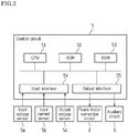
- control circuit 5 includes, as shown in FIG. 2 for example, a CPU 51, a ROM 52, a RAM 53, an input interface 54 and an output interface 55.
- the control circuit 5 may include devices other than the above-described digital devices.
- the CPU 51 executes programs and the like that are stored in the ROM 52.
- the ROM 52 stores programs, set values to be used at the time of executing the programs, and the like.
- the RAM 53 has a function to temporarily store detection results by sensors and the like.
- an input voltage sensor 5a an input voltage sensor 5a, an input current sensor 5b and an output voltage sensor 5c are connected so that detection results are input to the input interface 54 from the respective sensors.
- the power factor correction circuit 2 and the auxiliary circuit 3 are connected so that drive signals are output from the output interface 55 to drive the transistors 22 and 33.
- the input voltage sensor 5a is provided to detect the input voltage that is output from the AC power supply 150 and that is input to the rectification circuit 1.
- the input current sensor 5b is provided to detect the input current that is input to the rectification circuit 1.
- the output voltage sensor 5c is provided to detect the output voltage that is output to the load 160.
- control circuit 5 allows the auxiliary circuit 3 to operate for a certain period in the half cycle of the AC power supply 150, and does not allow the auxiliary circuit 3 to operate for the other period, which is other than the certain period, in the half cycle of the AC power supply 150.
- the certain period is a period in which the loss in operation of the auxiliary circuit 3 is less than the switching loss in the transistor 22.
- the other period is a period in which the loss in operation of the auxiliary circuit 3 is more than the switching loss in the transistor 22.
- the certain period includes a period in which the absolute value of the input voltage from the AC power supply 150 is maximum while the other period includes a period in which the absolute value of the input voltage from the AC power supply 150 is minimum.
- the control circuit 5 determines that the power supply device 100 is in the certain period and brings the auxiliary circuit 3 to the operating state.
- the control circuit 5 determines that the power supply device 100 is in the other period and brings the auxiliary circuit 3 to the non-operating state.
- the predetermined value which is determined according to, for example, a circuit design and an operating condition, may be stored in advance in the ROM 52 and the like, or may be calculated by the CPU 51 based on information stored in the ROM 52 and the like.
- the transistor 22 is switched by the control circuit 5 at a predetermined period, thus the input current that is input to the rectification circuit 1 is formed into the sinusoidal waveform. Then, if the power supply device 100 is in the certain period in the half cycle of the AC power supply 150, the auxiliary circuit 3 is operated, which means that the transistor 33 is turned on before the transistor 22 that has been turned on is turned off. Thus, the current that flows through the transistor 22 is drawn out, and the transistor 22 is turned off under ZCS condition.
- description is given on the operation in a predetermined one period in case of the certain period.
- I Tr22 includes the current flowing through the diode 22a that is a parasitic diode.
- the transistor 22 and the transistor 33 are being turned off.
- the current from the rectification circuit 1 is output to the side of the smoothing capacitor 4 via the inductor 21, the diode 23, the inductor 31 and the diode 35.
- the transistor 22 when the transistor 22 is turned on at the time point t0, the current from the inductor 21 flows to the transistor 22, which results in decrease in the current that is output to the smoothing capacitor 4 via the diode 23, the inductor 31 and the diode 35.
- the transistor 22 is turned on in a state in which no current flows through the transistor 22, thus it is performed under ZCS condition.
- the inductor 31 and the capacitor 32 start to resonate.
- the capacitor 32 discharges and the current flows through the inductor 31, the diode 34 and the transistor 33.
- the direction of the current that flows through the inductor 31 is reversed.
- the diode 34 prevents the backflow of the current, the current, which has flown from the inductor 21 to the transistor 22, flows to the inductor 31 via the diode 23, which results in rapid decrease in the current that flows through the transistor 22.
- the diode 22a is conducted. In this way, when the current flows through the diode 22a, no current flows through the transistor 22. Then, when 3/4 of the resonant period has elapsed (i.e., when the current that flows through the diode 22a is maximum), the transistor 22 is turned off. Thus, the transistor 22 is turned off under ZCS condition. The transistor 33 is also turned off at the same time as the turn-off of the transistor 22.
- the current stops flowing through the diode 22a, and at the time point t6, the capacitor 32 is fully charged. Then, from the time point t6, the current is output to the side of the smoothing capacitor 4 via the diode 35.
- auxiliary circuit 3 since the auxiliary circuit 3 is provided as described above, it is possible to draw the current from the transistor 22 by the auxiliary circuit 3 before the transistor 22 is turned off, which results in reduction in the turn-off loss.
- the output power was set to 240W.
- the input voltage (output voltage of the AC power supply 150) V AC was set to 100Vrms, and the frequency f AC of the AC power supply 150 was set to 60Hz.
- the output voltage Vo of the power supply device 100 was set to 385V, and the capacitance of the smoothing capacitor 4 was set to 1mF.
- the switching frequency fsw of the transistor 22 of the power factor correction circuit 2 was set to 200kHz, and the inductance of the inductor 21 of the power factor correction circuit 2 was set to 800 ⁇ H.
- the inductance of the inductor 31 of the auxiliary circuit 3 was set to 3.3 ⁇ H, and the capacitance of the capacitor 32 of the auxiliary circuit 3 was set to 0.5nF.
- the resonant period Ta was 0.255 ⁇ s.
- FIG. 4 is a graph that indicates the relationship of the current I Tr22 and the voltage V Tr22 between the drain and the source of the transistor 22. From the current waveform and the voltage waveform indicated in FIG. 4 , it was confirmed that the transistor 22 was turned off under ZCS condition.
- the auxiliary circuit 3 when the auxiliary circuit 3 is provided and operated, the current caused by the resonance flows through the inductor 31, the diode 34 and the transistor 33, which results in loss (conduction loss) in the auxiliary circuit 3.
- the auxiliary circuit 3 is brought to the operating state when the power supply device 100 is in the certain period in the half cycle of the AC power supply 150 (i.e., in the period in which the loss in the auxiliary circuit 3 is less than the turn-off loss in the transistor 22).
- the auxiliary circuit 3 is brought to the non-operating state when the power supply device 100 is in the other period in the half cycle of the AC power supply 150 (i.e., in the period in which the loss in the auxiliary circuit 3 is more than the turn-off loss in the transistor 22).
- the turn-off loss in the transistor 22 can be reduced by switching the transistor 33 by the control circuit 5. However, the conduction loss is generated by the resonance in the auxiliary circuit 3. On the other hand, when the auxiliary circuit 3 is not operated, the transistor 33 is being turned off, thus the conduction loss is not generated by the resonance in the auxiliary circuit 3. However, the turn-off loss in the transistor 22 is generated.
- the auxiliary circuit 3 is brought to the non-operating state when the loss in the auxiliary circuit 3 is more than the turn-off loss.
- the power supply device 100 is determined, for example, based on the absolute value of the input voltage from the AC power supply 150.
- P L31_LOSS represents the conduction loss in the inductor 31
- P D34_LOSS represents the conduction loss in the diode 34
- P Tr33_LOSS represents the conduction loss in the transistor 33.
- Ta represents the resonant period
- I L31 represents the current that flows through the inductor 31
- R L31 represents the resistance of a copper wire of the inductor 31.
- Ta represents the resonant period
- V D34 represents the voltage (forward voltage drop) between the terminals of the diode 34
- I D34 represents the current that flows through the diode 34.
- Ta represents the resonant period
- I Tr33 represents the current that flows through the transistor 33
- R Tr33 represents the ON-resistance of the transistor 33.
- Tswoff represents the turn-off time
- I Tr22 represents the current between the drain and the source of the transistor 22
- V Tr22 represents the voltage between the drain and the source of the transistor 22.
- the relationship of the loss P 3_LOSS in the auxiliary circuit 3 and the turn-off loss P SWOFF_LOSS was obtained by simulation.
- the combined resistance in the auxiliary circuit 3 was set to 0.8 ⁇ and the forward voltage drop in the diode 34 was set to 0.867V, in addition to the above-described set values. The results are indicated in FIG. 5 .
- the loss P 3_LOSS in the auxiliary circuit 3 was substantially constant regardless of the absolute value of the input voltage V AC .
- the turn-off loss P SWOFF_LOSS was increased. Accordingly, when the absolute value of the input voltage V AC was not more than 45V, the loss P 3_LOSS in the auxiliary circuit 3 was more than the turn-off loss P SWOFF_LOSS , and when the absolute value of the input voltage V AC was more than 45V, the loss P 3-LOSS in the auxiliary circuit 3 was less than the turn-off loss P SWOFF_LOSS .
- the absolute value of the input voltage V AC is not more than the predetermined value (for example, 45V)
- the predetermined value for example, 45V
- the absolute value of the input voltage V AC is more than the predetermined value, it is more efficient to determine that the power supply device 100 is in the certain period and to bring the auxiliary circuit 3 to the operating state so that the turn-off loss P SWOFF_LOSS is reduced.
- the auxiliary circuit 3 when the absolute value of the input voltage V AC is more than the predetermined value, the auxiliary circuit 3 is brought to the operating state, and when the absolute value of the input voltage V AC is not more than the predetermined value, the auxiliary circuit 3 is brought to the non-operating state. Thus, it is possible to further reduce the loss in the power supply device 100 as a whole.
- the present invention is exemplarily applied to the power supply device 100.
- the present invention is not limited thereto.
- the present invention may be applied to another electronic circuit.
- the single-phase power supply device 100 is exemplarily described.
- the present invention is not limited thereto.
- the present invention may be applied to a three-phase power supply device.
- a low-pass filter (not shown) for removing high-frequency components of the input current may be provided between the AC power supply 150 and the rectification circuit 1.
- whether the power supply device 100 is in the certain period or in the other period is exemplarily determined based on the absolute value of the input voltage from the AC power supply 150.
- the present invention is not limited thereto. Whether the power supply device 100 is in the certain period or in the other period may be determined based on the output voltage from the rectification circuit.
- the present invention is suitable for an electronic circuit including a power factor correction circuit and for a method for controlling the electronic circuit.
Landscapes
- Engineering & Computer Science (AREA)
- Power Engineering (AREA)
- Rectifiers (AREA)
Abstract
Description
- The present invention relates to an electronic circuit and a method for controlling the electronic circuit.
- Conventionally, power supply devices (electronic circuits) are known, in which an AC voltage input from an AC power supply is converted into a DC voltage so as to be output to a load. One example of the power supply devices includes a power supply device including a full-wave rectification circuit and a smoothing capacitor provided on an output side of the full-wave rectification circuit. However, in such a power supply device, there is a problem that the waveform of an input current is distorted. Thus, a power supply device including a power factor correction circuit (PFC) has been conventionally proposed to form the waveform of the input current into a sinusoidal waveform. The power factor correction circuit includes, for example, an inductor and a switching element that controls the current flowing through the inductor.
- Mohammad, Mahdavi. and Hosein Farzanehfard. "Zero-Current-Transition Bridgeless PFC Without Extra Voltage and Current Stress." IEEE Transactions on Industrial Electronics, volume 56, no.7, July 2009.
- Here, in the power supply device with the power factor correction circuit as described above, the switching element is turned off when the current is flowing, which generates switching loss. In order to reduce the switching loss, an auxiliary circuit disclosed in Non-Patent
Document 1 may be applied to the power supply device. - When the auxiliary circuit is provided in the power supply device, the auxiliary circuit can draw the current from the switching element. Thus, the switching element is turned off when no current is flowing, that is, ZCS (zero current switching) is performed. In this way, it is possible to reduce the switching loss.
- Operating the auxiliary circuit makes possible to reduce the switching loss, however, it also generates loss (conduction loss) in the auxiliary circuit.
- The present invention was made in consideration of the above problem, an object of which is to provide an electronic circuit capable of reducing loss in a device as a whole and a method for controlling the electronic circuit.
- An electronic circuit according to the present invention includes: a rectification circuit that rectifies an AC voltage input from an AC power supply; a power factor correction circuit that includes a first switching element and that shapes a current which is input, by the first switching element being driven, from the AC power supply to the rectification circuit; an auxiliary circuit that reduces switching loss in the first switching element by drawing the current from the rectification circuit before the first switching element is turned off so that the current that flows through the first switching element is reduced; and a control circuit that allows the auxiliary circuit to operate for a certain period in a half cycle of the AC power supply, and that does not allow the auxiliary circuit to operate for the other period, which is other than the certain period, in the half cycle of the AC power supply.
- In the above-described electronic circuit, the certain period may be a period in which loss in operation of the auxiliary circuit is less than the switching loss, and the other period may be a period in which the loss in operation of the auxiliary circuit is more than the switching loss. The switching loss in the first switching element means loss that is generated in the first switching element by not operating the auxiliary circuit when the electronic circuit is operated. Accordingly, the switching loss in the first switching element is, for example, an integrated value of the product of the current and the voltage at the turn-off time. Also, the loss in operation of the auxiliary circuit means loss that is generated by operating the auxiliary circuit when the electronic circuit is operated. Accordingly, the loss in operation of the auxiliary circuit is, for example, a sum of conduction loss of the respective elements disposed in the auxiliary circuit.
- In the above-described electronic circuit, the certain period may include a period in which an absolute value of the input voltage from the AC power supply is maximum, and the other period may include a period in which the absolute value of the input voltage from the AC power supply is minimum.
- In the above-described electronic circuit, the control circuit may determine that the electronic circuit is in the certain period when the absolute value of the input voltage from the AC power supply is more than a predetermined value, and may determine that the electronic circuit is in the other period when the absolute value of the input voltage from the AC power supply is not more than the predetermined value. The predetermined value is determined according to, for example, a circuit design and an operating condition.
- In the above-described electronic circuit, the auxiliary circuit may include: an inductor that is disposed in a positive pole line; a second switching element and a diode that are disposed on one end side of the inductor; and a capacitor that is disposed on the other end side of the inductor. The capacitor may be connected between the positive pole line and a negative pole line, and the second switching element and the diode may be connected in series between the positive pole line and the negative pole line. When the auxiliary circuit is operated, the second switching element may be turned on before the first switching element that has been turned on is turned off.
- In a method for controlling an electronic circuit according to the present invention, the electronic circuit includes: a rectification circuit that rectifies an AC voltage input from an AC power supply; a power factor correction circuit that includes a first switching element and that shapes a current which is input, by the first switching element being driven, from the AC power supply to the rectification circuit; an auxiliary circuit that reduces switching loss in the first switching element by drawing the current from the rectification circuit before the first switching element is turned off so that the current that flows through the first switching element is reduced. The method includes the steps of: determining whether the electronic circuit is, in a half cycle of the AC power supply, in a certain period or in the period other than the certain period; and allowing the auxiliary circuit to operate when the electronic circuit is in the certain period, and not allowing the auxiliary circuit to operate when the electronic circuit is in the other period.
- In the method for controlling the electronic circuit, the certain period may be a period in which the loss in operation of the auxiliary circuit is less than the switching loss, and the other period may be a period in which the loss in operation of the auxiliary circuit is more than the switching loss.
- With the electronic circuit and the method for controlling the electronic circuit according to the present invention, it is possible to reduce loss in a device as a whole.
-
- [
FIG.1 ]
FIG. 1 is a circuit diagram of a power supply device according to an embodiment of the present invention. - [
FIG. 2 ]
FIG. 2 is a block diagram showing a control circuit of the power supply device inFIG. 1 . - [
FIG. 3 ]
FIG. 3 is a timing chart for explaining operations of the power supply device inFIG. 1 . - [
FIG. 4 ]
FIG. 4 is a graph showing a current waveform and a voltage waveform of a transistor, which were obtained by simulation. - [
FIG. 5 ]
FIG. 5 is a graph showing a relationship of turn-off loss and loss in an auxiliary circuit, which was obtained by simulation. - Hereinafter, description will be given on an embodiment of the present invention with reference to the drawings.
- First, a circuit configuration of a
power supply device 100 according to an embodiment of the present invention is described with reference toFIGS. 1 and2 . Note that thepower supply device 100 is one example of the "electronic circuit" of the present invention. - As shown in
FIG. 1 , thepower supply device 100 includes: arectification circuit 1; a powerfactor correction circuit 2; anauxiliary circuit 3; asmoothing capacitor 4; and a control circuit 5 (seeFIG. 2 ). An AC power supply (commercial power supply) 150 is connected to an input side of thepower supply device 100, and aload 160 is connected to an output side of thepower supply device 100. Thus, thepower device 100 is configured to convert an AC voltage input from theAC power supply 150 into a DC voltage and to output the DC voltage to theload 160. - The
rectification circuit 1 is provided to rectify the positive/negative voltage input from theAC power supply 150 in a positive direction. Therectification circuit 1 is disposed between theAC power supply 150 and the powerfactor correction circuit 2. Therectification circuit 1 is, for example, a full-wave rectification bridge circuit that includes fourdiodes 11 to 14. - The
diode 11 and thediode 13 are connected in series. One output end of theAC power supply 150 is connected between thediode 11 and thediode 13. A cathode of thediode 11 is connected to apositive pole line 50 via elements (specifically, aninductor 21, adiode 23, aninductor 31 and adiode 35, described later) while an anode of thediode 13 is connected to anegative pole line 60. Thediode 12 and thediode 14 are connected in series. The other output end of theAC power supply 150 is connected between thediode 12 and thediode 14. A cathode of thediode 12 is connected to thepositive pole line 50 via the elements (specifically, theinductor 21, thediode 23, theinductor 31 and thediode 35, described later) while an anode of thediode 14 is connected to thenegative pole line 60. - The power
factor correction circuit 2 is provided to form an input current that is input from theAC power supply 150 to therectification circuit 1 into a sinusoidal waveform. The powerfactor correction circuit 2 is disposed between therectification circuit 1 and theauxiliary circuit 3. The powerfactor correction circuit 2 includes theinductor 21, atransistor 22 controlling the current flowing through theinductor 21, and the step-updiode 23. Note that thetransistor 22 is one example of the "first switching element" of the present invention. - The
inductor 21 and thediode 23 are arranged in series in thepositive pole line 50. One end of theinductor 21 is connected to therectification circuit 1, and the other end thereof is connected to an anode of thediode 23. A cathode of thediode 23 is connected to theauxiliary circuit 3. That is, theinductor 21 is disposed on the side of therectification circuit 1 while thediode 23 is disposed on the side of theauxiliary circuit 3. - The
transistor 22 is connected between thepositive pole line 50 and thenegative pole line 60. A source of thetransistor 22 is connected to thenegative pole line 60, and a drain thereof is connected to thepositive pole line 50 between theinductor 21 and thediode 23. Thecontrol circuit 5 is connected to a gate of thetransistor 22 so that a drive signal is input to the gate. Also, adiode 22a is connected in anti-parallel to thetransistor 22. For example, thetransistor 22 is a MOSFET and thediode 22a is a parasitic diode. - The
auxiliary circuit 3 is provided to reduce switching loss in thetransistor 22. Specifically, theauxiliary circuit 3 draws the current from therectification circuit 1 before thetransistor 22 is turned off so as to reduce the current that flows through thetransistor 22. Thus, thetransistor 22 is turned off when no current is flowing therethrough. That is, theauxiliary circuit 3 is provided to turn off thetransistor 22 under ZCS condition. Theauxiliary circuit 3 is disposed between the powerfactor correction circuit 2 and the smoothingcapacitor 4. - The
auxiliary circuit 3 includes: theinductor 31 and acapacitor 32 that constitute a resonant circuit; atransistor 33 and adiode 34 that control the resonance; and thediode 35 for preventing backflow. Note that thetransistor 33 is one example of the "second switching element" of the present invention. - The
inductor 31 and thediode 35 are arranged in series in thepositive pole line 50. One end of theinductor 31 is connected to the cathode of thediode 23, and the other end thereof is connected to an anode of thediode 35. A cathode of thediode 35 is connected to the smoothingcapacitor 4. That is, theinductor 31 is disposed on the side of the powerfactor correction circuit 2 while thediode 35 is disposed on the side of the smoothingcapacitor 4. Thecapacitor 32 is disposed on the other end side of theinductor 31, and is connected between thenegative pole line 60 and thepositive pole line 50 that is between theinductor 31 and thediode 35. - The
transistor 33 and thediode 34 are disposed on the one end side of theinductor 31, and are connected in series between thepositive pole line 50 and thenegative pole line 60. A source of thetransistor 33 is connected to thenegative pole line 60, and a drain thereof is connected to a cathode of thediode 34. Thecontrol circuit 5 is connected to a gate of thetransistor 33 so that a drive signal is input to the gate. Also, adiode 33a is connected in anti-parallel to thetransistor 33. For example, thetransistor 33 is a MOSFET and thediode 33a is a parasitic diode. An anode of thediode 34 is connected to thepositive pole line 50 between theinductor 31 and thediode 23. That is, thecapacitor 32, theinductor 31, thediode 34 and thetransistor 33 are connected in series. - Here, in this embodiment, the
auxiliary circuit 3 can be switched between an operating state and a non-operating state. It is switched to the operating state when loss in operation (conduction loss) is less than the switching loss in thetransistor 22 while it is switched to the non-operating state when the loss in operation is more than the switching loss in thetransistor 22. This will be described in detail later. - The smoothing
capacitor 4 is provided to smooth the output of therectification circuit 1. The smoothingcapacitor 4 is, for example, an electrolytic capacitor that is disposed between theauxiliary circuit 3 and theload 160 and that is connected between thepositive pole line 50 and thenegative pole line 60. Both ends of theload 160 are respectively connected to thepositive pole line 50 and thenegative pole line 60. - The
control circuit 5 is provided to allow thepower supply device 100 to operate. Thecontrol circuit 5 drives thetransistor 22 so as to allow the powerfactor correction circuit 2 to operate. Thecontrol circuit 5 also drives thetransistor 33 so as to bring theauxiliary circuit 3 to the operating state, and does not drive thetransistor 33 so as to bring theauxiliary circuit 3 to the non-operating state. - Specifically, the
control circuit 5 includes, as shown inFIG. 2 for example, aCPU 51, aROM 52, aRAM 53, aninput interface 54 and anoutput interface 55. Thecontrol circuit 5 may include devices other than the above-described digital devices. - The
CPU 51 executes programs and the like that are stored in theROM 52. TheROM 52 stores programs, set values to be used at the time of executing the programs, and the like. TheRAM 53 has a function to temporarily store detection results by sensors and the like. - To the
input interface 54, for example, aninput voltage sensor 5a, an inputcurrent sensor 5b and anoutput voltage sensor 5c are connected so that detection results are input to theinput interface 54 from the respective sensors. To theoutput interface 55, for example, the powerfactor correction circuit 2 and theauxiliary circuit 3 are connected so that drive signals are output from theoutput interface 55 to drive thetransistors - The
input voltage sensor 5a is provided to detect the input voltage that is output from theAC power supply 150 and that is input to therectification circuit 1. The inputcurrent sensor 5b is provided to detect the input current that is input to therectification circuit 1. Theoutput voltage sensor 5c is provided to detect the output voltage that is output to theload 160. - In this embodiment, the
control circuit 5 allows theauxiliary circuit 3 to operate for a certain period in the half cycle of theAC power supply 150, and does not allow theauxiliary circuit 3 to operate for the other period, which is other than the certain period, in the half cycle of theAC power supply 150. - For example, the certain period is a period in which the loss in operation of the
auxiliary circuit 3 is less than the switching loss in thetransistor 22. The other period is a period in which the loss in operation of theauxiliary circuit 3 is more than the switching loss in thetransistor 22. Also, the certain period includes a period in which the absolute value of the input voltage from theAC power supply 150 is maximum while the other period includes a period in which the absolute value of the input voltage from theAC power supply 150 is minimum. - When the absolute value of the input voltage from the
AC power supply 150 is more than a predetermined value, thecontrol circuit 5 determines that thepower supply device 100 is in the certain period and brings theauxiliary circuit 3 to the operating state. When the absolute value of the input voltage from theAC power supply 150 is not more than the predetermined value, thecontrol circuit 5 determines that thepower supply device 100 is in the other period and brings theauxiliary circuit 3 to the non-operating state. The predetermined value, which is determined according to, for example, a circuit design and an operating condition, may be stored in advance in theROM 52 and the like, or may be calculated by theCPU 51 based on information stored in theROM 52 and the like. - Next, description is given on operations of the
power supply device 100 with reference toFIGS. 1 to 3 . In thepower supply device 100, thetransistor 22 is switched by thecontrol circuit 5 at a predetermined period, thus the input current that is input to therectification circuit 1 is formed into the sinusoidal waveform. Then, if thepower supply device 100 is in the certain period in the half cycle of theAC power supply 150, theauxiliary circuit 3 is operated, which means that thetransistor 33 is turned on before thetransistor 22 that has been turned on is turned off. Thus, the current that flows through thetransistor 22 is drawn out, and thetransistor 22 is turned off under ZCS condition. Hereinafter, description is given on the operation in a predetermined one period in case of the certain period. - In the waveform chart in
FIG. 3 , the respective reference numerals represent the following, in order from the top: Tr22 represents the on/off state of thetransistor 22; Tr33 represents the on/off state of thetransistor 33; VC32 represents the voltage of thecapacitor 32; IL31 represents the current of theinductor 31; ITr22 represents the current between the drain and the source of thetransistor 22; VTr22 represents the voltage between the drain and the source of thetransistor 22; ITr33 represents the current between the drain and the source of thetransistor 33; VTr33 represents the voltage between the drain and the source of thetransistor 33; ID23 represents the current of thediode 23; VD23 represents the voltage between the terminals of thediode 23; ID35 represents the current of thediode 35; and VD35 represents the voltage between the terminals of thediode 35. ITr22 includes the current flowing through thediode 22a that is a parasitic diode. - Before the time point t0, the
transistor 22 and thetransistor 33 are being turned off. The current from therectification circuit 1 is output to the side of the smoothingcapacitor 4 via theinductor 21, thediode 23, theinductor 31 and thediode 35. - Then, when the
transistor 22 is turned on at the time point t0, the current from theinductor 21 flows to thetransistor 22, which results in decrease in the current that is output to the smoothingcapacitor 4 via thediode 23, theinductor 31 and thediode 35. Here, thetransistor 22 is turned on in a state in which no current flows through thetransistor 22, thus it is performed under ZCS condition. - From the time point t1 when the current stops flowing through the
diode 23, theinductor 31 and thediode 35, the current from theinductor 21 completely flows to thetransistor 22. At this time, energy is accumulated in theinductor 21, which results in increase in the current that flows through theinductor 21 and thetransistor 22. - After that, when the
transistor 33 is turned on at the time point t2, theinductor 31 and thecapacitor 32 start to resonate. Thus, thecapacitor 32 discharges and the current flows through theinductor 31, thediode 34 and thetransistor 33. Then, at the time point t3 when 1/2 of the resonant period has elapsed, the direction of the current that flows through theinductor 31 is reversed. At this time, since thediode 34 prevents the backflow of the current, the current, which has flown from theinductor 21 to thetransistor 22, flows to theinductor 31 via thediode 23, which results in rapid decrease in the current that flows through thetransistor 22. - Then, from the time point t4 when the current that flows through the
transistor 22 becomes zero, thediode 22a is conducted. In this way, when the current flows through thediode 22a, no current flows through thetransistor 22. Then, when 3/4 of the resonant period has elapsed (i.e., when the current that flows through thediode 22a is maximum), thetransistor 22 is turned off. Thus, thetransistor 22 is turned off under ZCS condition. Thetransistor 33 is also turned off at the same time as the turn-off of thetransistor 22. - After that, at the time point t5, the current stops flowing through the
diode 22a, and at the time point t6, thecapacitor 32 is fully charged. Then, from the time point t6, the current is output to the side of the smoothingcapacitor 4 via thediode 35. - The above-described operations are repeatedly performed.
- In this embodiment, since the
auxiliary circuit 3 is provided as described above, it is possible to draw the current from thetransistor 22 by theauxiliary circuit 3 before thetransistor 22 is turned off, which results in reduction in the turn-off loss. - Next, description is given on simulation that was performed in order to confirm the effect of this embodiment. The simulation was performed using a circuit simulator LTspice.
- As the simulation conditions, the output power was set to 240W. The input voltage (output voltage of the AC power supply 150) VAC was set to 100Vrms, and the frequency fAC of the
AC power supply 150 was set to 60Hz. The output voltage Vo of thepower supply device 100 was set to 385V, and the capacitance of the smoothingcapacitor 4 was set to 1mF. The switching frequency fsw of thetransistor 22 of the powerfactor correction circuit 2 was set to 200kHz, and the inductance of theinductor 21 of the powerfactor correction circuit 2 was set to 800µH. The inductance of theinductor 31 of theauxiliary circuit 3 was set to 3.3µH, and the capacitance of thecapacitor 32 of theauxiliary circuit 3 was set to 0.5nF. Thus, the resonant period Ta was 0.255µs. - The results of the simulation are indicated in
FIG. 4. FIG. 4 is a graph that indicates the relationship of the current ITr22 and the voltage VTr22 between the drain and the source of thetransistor 22. From the current waveform and the voltage waveform indicated inFIG. 4 , it was confirmed that thetransistor 22 was turned off under ZCS condition. - Here, as in this embodiment, when the
auxiliary circuit 3 is provided and operated, the current caused by the resonance flows through theinductor 31, thediode 34 and thetransistor 33, which results in loss (conduction loss) in theauxiliary circuit 3. - For this reason, in the
power supply device 100 of this embodiment, theauxiliary circuit 3 is brought to the operating state when thepower supply device 100 is in the certain period in the half cycle of the AC power supply 150 (i.e., in the period in which the loss in theauxiliary circuit 3 is less than the turn-off loss in the transistor 22). Theauxiliary circuit 3 is brought to the non-operating state when thepower supply device 100 is in the other period in the half cycle of the AC power supply 150 (i.e., in the period in which the loss in theauxiliary circuit 3 is more than the turn-off loss in the transistor 22). - When the
auxiliary circuit 3 is operated, the turn-off loss in thetransistor 22 can be reduced by switching thetransistor 33 by thecontrol circuit 5. However, the conduction loss is generated by the resonance in theauxiliary circuit 3. On the other hand, when theauxiliary circuit 3 is not operated, thetransistor 33 is being turned off, thus the conduction loss is not generated by the resonance in theauxiliary circuit 3. However, the turn-off loss in thetransistor 22 is generated. - With the above-described configuration, when the
power supply device 100 is in the certain period (i.e., in the period in which the loss in theauxiliary circuit 3 is less than the turn-off loss), it is possible to reduce the turn-off loss by bringing theauxiliary circuit 3 to the operating state, and when thepower supply device 100 is in the other period (i.e., in the period in which the loss in theauxiliary circuit 3 is more than the turn-off loss), it is possible to eliminate the loss in theauxiliary circuit 3 by bringing theauxiliary circuit 3 to the non-operating state. Thus, it is possible to reduce the loss in thepower supply device 100 as a whole. That is, in the case where theauxiliary circuit 3 is provided to reduce the turn-off loss, theauxiliary circuit 3 is brought to the non-operating state when the loss in theauxiliary circuit 3 is more than the turn-off loss. Thus, compared to the case in which theauxiliary circuit 3 is continuously operated, it is possible to further reduce the loss in thepower supply device 100 as a whole. Whether thepower supply device 100 is in the certain period or in the other period is determined, for example, based on the absolute value of the input voltage from theAC power supply 150. - Specifically, the loss P3_LOSS in the
auxiliary circuit 3 is expressed by the following equation (1):
[Mathematical 1]
- In the above equation (1), PL31_LOSS represents the conduction loss in the
inductor 31, PD34_LOSS represents the conduction loss in thediode 34, and PTr33_LOSS represents the conduction loss in thetransistor 33. - Also, the conduction loss PL31_LOSS in the
inductor 31 is expressed by the following equation (2):
[Mathematical 2]
- In the above equation (2), Ta represents the resonant period, IL31 represents the current that flows through the
inductor 31, and RL31 represents the resistance of a copper wire of theinductor 31. - Also, the conduction loss PD34_LOSS in the
diode 34 is expressed by the following equation (3):
[Mathematical 3]
- In the above equation (3), Ta represents the resonant period, VD34 represents the voltage (forward voltage drop) between the terminals of the
diode 34, and ID34 represents the current that flows through thediode 34. - Also, the conduction loss PTr33_LOSS in the
transistor 33 is expressed by the following equation (4):
[Mathematical 4]
- In the above equation (4), Ta represents the resonant period, ITr33 represents the current that flows through the
transistor 33, and RTr33 represents the ON-resistance of thetransistor 33. - Meanwhile, the turn-off loss PSWOFF_LOSS in the
transistor 22 is expressed by the following equation (5):
[Mathematical 5]
- In the above equation (5), Tswoff represents the turn-off time, ITr22 represents the current between the drain and the source of the
transistor 22, and VTr22 represents the voltage between the drain and the source of thetransistor 22. - In the
power supply device 100, since the value of the current that flows through thetransistor 22 changes according to the absolute value of the sinusoidal input voltage VAC that is input from theAC power supply 150, the value of the turn-off loss PSWOFF_LOSS also changes. - Then, the relationship of the loss P3_LOSS in the
auxiliary circuit 3 and the turn-off loss PSWOFF_LOSS was obtained by simulation. As the simulation conditions, the combined resistance in theauxiliary circuit 3 was set to 0.8Ω and the forward voltage drop in thediode 34 was set to 0.867V, in addition to the above-described set values. The results are indicated inFIG. 5 . - As can be seen from the graph in
FIG. 5 , the loss P3_LOSS in theauxiliary circuit 3 was substantially constant regardless of the absolute value of the input voltage VAC. In contrast, it was confirmed that as the absolute value of the input voltage VAC was increased, the turn-off loss PSWOFF_LOSS was increased. Accordingly, when the absolute value of the input voltage VAC was not more than 45V, the loss P3_LOSS in theauxiliary circuit 3 was more than the turn-off loss PSWOFF_LOSS, and when the absolute value of the input voltage VAC was more than 45V, the loss P3-LOSS in theauxiliary circuit 3 was less than the turn-off loss PSWOFF_LOSS. - Thus, it was found that when the absolute value of the input voltage VAC is not more than the predetermined value (for example, 45V), it is more efficient to determine that the
power supply device 100 is in the other period and to bring theauxiliary circuit 3 to the non-operating state so that the turn-off loss PSWOFF_LOSS is generated. Also, it was found that when the absolute value of the input voltage VAC is more than the predetermined value, it is more efficient to determine that thepower supply device 100 is in the certain period and to bring theauxiliary circuit 3 to the operating state so that the turn-off loss PSWOFF_LOSS is reduced. That is, when the absolute value of the input voltage VAC is more than the predetermined value, theauxiliary circuit 3 is brought to the operating state, and when the absolute value of the input voltage VAC is not more than the predetermined value, theauxiliary circuit 3 is brought to the non-operating state. Thus, it is possible to further reduce the loss in thepower supply device 100 as a whole. - The embodiment described herein is to be considered in all respects as illustrative and not limiting. The technical scope of the present invention is indicated by the appended claims rather than by the foregoing embodiment, and all modifications and changes that come within the meaning and range of equivalency of the claims are intended to be embraced therein.
- In this embodiment, the present invention is exemplarily applied to the
power supply device 100. However, the present invention is not limited thereto. The present invention may be applied to another electronic circuit. - Also, in this embodiment, the single-phase
power supply device 100 is exemplarily described. However, the present invention is not limited thereto. The present invention may be applied to a three-phase power supply device. - Also, in this embodiment, a low-pass filter (not shown) for removing high-frequency components of the input current may be provided between the
AC power supply 150 and therectification circuit 1. - Also, in this embodiment, whether the
power supply device 100 is in the certain period or in the other period is exemplarily determined based on the absolute value of the input voltage from theAC power supply 150. However, the present invention is not limited thereto. Whether thepower supply device 100 is in the certain period or in the other period may be determined based on the output voltage from the rectification circuit. - The present invention is suitable for an electronic circuit including a power factor correction circuit and for a method for controlling the electronic circuit.
-
- 1
- Rectification circuit
- 2
- Power factor correction circuit
- 3
- Auxiliary circuit
- 5
- Control circuit
- 22
- Transistor (first switching element)
- 31
- Inductor
- 32
- Capacitor
- 33
- Transistor (second switching element)
- 34
- Diode
- 50
- Positive pole line
- 60
- Negative pole line
- 100
- Power supply device (electronic circuit)
- 150
- AC power supply
Claims (7)
- An electronic circuit, comprising:a rectification circuit being configured to rectify an AC voltage input from an AC power supply;a power factor correction circuit including a first switching element, the power factor correction circuit being configured to shape a current that is input, by the first switching element being driven, from the AC power supply to the rectification circuit;an auxiliary circuit being configured to reduce switching loss in the first switching element by drawing the current from the rectification circuit before the first switching element is turned off so that the current that flows through the first switching element is reduced; anda control circuit being configured to allow the auxiliary circuit to operate for a first period in a half cycle of the AC power supply, and to not allow the auxiliary circuit to operate for a second period in the half cycle of the AC power supply, the second period being other than the first period.
- The electronic circuit according to claim 1,
wherein the first period is a period in which loss in operation of the auxiliary circuit is less than the switching loss, and
wherein the second period is a period in which the loss in operation of the auxiliary circuit is more than the switching loss. - The electronic circuit according to claim 1 or 2,
wherein the first period includes a period in which an absolute value of the input voltage from the AC power supply is maximum, and
wherein the second period includes a period in which the absolute value of the input voltage from the AC power supply is minimum. - The electronic circuit according to any one of claims 1 to 3,
wherein the control circuit determines that the electronic circuit is in the first period when an absolute value of the input voltage from the AC power supply is more than a predetermined value, and
wherein the control circuit determines that the electronic circuit is in the second period when the absolute value of the input voltage from the AC power supply is not more than the predetermined value. - The electronic circuit according to any one of claims 1 to 4,
wherein the auxiliary circuit includes: an inductor that is disposed in a positive pole line; a second switching element and a diode that are disposed on one end side of the inductor; and a capacitor that is disposed on another end side of the inductor,
wherein the capacitor is connected between the positive pole line and a negative pole line while the second switching element and the diode are connected in series between the positive pole line and the negative pole line, and
wherein, when the auxiliary circuit is operated, the second switching element is turned on before the first switching element that has been turned on is turned off. - A method for controlling an electronic circuit, the electronic circuit including:a rectification circuit being configured to rectify an AC voltage input from an AC power supply;a power factor correction circuit including a first switching element, the power factor correction circuit being configured to shape a current that is input, by the first switching element being driven, from the AC power supply to the rectification circuit; andan auxiliary circuit being configured to reduce switching loss in the first switching element by drawing the current from the rectification circuit before the first switching element is turned off so that the current that flows through the first switching element is reduced,the method comprising the steps of:determining whether the electronic circuit is, in a half cycle of the AC power supply, in a first period or in a second period other than the first period; andallowing the auxiliary circuit to operate when the electronic circuit is in the first period, and not allowing the auxiliary circuit to operate when the electronic circuit is in the second period.
- The method for controlling an electronic circuit according to claim 6,
wherein the first period is a period in which loss in operation of the auxiliary circuit is less than the switching loss, and
wherein the second period is a period in which the loss in operation of the auxiliary circuit is more than the switching loss.
Applications Claiming Priority (2)
| Application Number | Priority Date | Filing Date | Title |
|---|---|---|---|
| JP2014184165A JP2016059178A (en) | 2014-09-10 | 2014-09-10 | Electronic circuit and control method for the electronic circuit |
| PCT/JP2015/074668 WO2016039205A1 (en) | 2014-09-10 | 2015-08-31 | Electronic circuit and electronic circuit control method |
Publications (2)
| Publication Number | Publication Date |
|---|---|
| EP3193439A1 true EP3193439A1 (en) | 2017-07-19 |
| EP3193439A4 EP3193439A4 (en) | 2017-08-23 |
Family
ID=55458957
Family Applications (1)
| Application Number | Title | Priority Date | Filing Date |
|---|---|---|---|
| EP15839562.4A Withdrawn EP3193439A4 (en) | 2014-09-10 | 2015-08-31 | Electronic circuit and electronic circuit control method |
Country Status (6)
| Country | Link |
|---|---|
| US (1) | US20170237338A1 (en) |
| EP (1) | EP3193439A4 (en) |
| JP (1) | JP2016059178A (en) |
| CN (1) | CN106537751A (en) |
| TW (1) | TW201618443A (en) |
| WO (1) | WO2016039205A1 (en) |
Family Cites Families (9)
| Publication number | Priority date | Publication date | Assignee | Title |
|---|---|---|---|---|
| KR100342457B1 (en) * | 1994-02-10 | 2002-11-02 | 코닌클리케 필립스 일렉트로닉스 엔.브이. | High frequency ac/ac converter with power factor correction |
| JP4289000B2 (en) * | 2003-04-22 | 2009-07-01 | サンケン電気株式会社 | Power factor correction circuit |
| JP2006067730A (en) * | 2004-08-27 | 2006-03-09 | Sanken Electric Co Ltd | Power factor improving circuit |
| JP2006223008A (en) * | 2005-02-08 | 2006-08-24 | Hitachi Ltd | DC-DC converter |
| JP4679332B2 (en) * | 2005-10-24 | 2011-04-27 | 三菱電機株式会社 | Resonant converter |
| JPWO2010061654A1 (en) * | 2008-11-25 | 2012-04-26 | 株式会社村田製作所 | PFC converter |
| JP5176922B2 (en) * | 2008-12-09 | 2013-04-03 | トヨタ自動車株式会社 | DC-DC converter and control method thereof |
| CN102696169B (en) * | 2010-01-05 | 2015-06-10 | 株式会社日立制作所 | AC-DC converter and its control method |
| CN203522524U (en) * | 2013-10-28 | 2014-04-02 | 南宁一举医疗电子有限公司 | X-ray machine power factor correction circuit based on zero-voltage transition soft switching |
-
2014
- 2014-09-10 JP JP2014184165A patent/JP2016059178A/en active Pending
-
2015
- 2015-08-31 CN CN201580040165.4A patent/CN106537751A/en not_active Withdrawn
- 2015-08-31 US US15/328,213 patent/US20170237338A1/en not_active Abandoned
- 2015-08-31 EP EP15839562.4A patent/EP3193439A4/en not_active Withdrawn
- 2015-08-31 WO PCT/JP2015/074668 patent/WO2016039205A1/en not_active Ceased
- 2015-09-08 TW TW104129583A patent/TW201618443A/en unknown
Also Published As
| Publication number | Publication date |
|---|---|
| WO2016039205A1 (en) | 2016-03-17 |
| JP2016059178A (en) | 2016-04-21 |
| CN106537751A (en) | 2017-03-22 |
| EP3193439A4 (en) | 2017-08-23 |
| US20170237338A1 (en) | 2017-08-17 |
| TW201618443A (en) | 2016-05-16 |
Similar Documents
| Publication | Publication Date | Title |
|---|---|---|
| JP6859034B2 (en) | Circuits and methods for synchronous rectification in resonant transducers | |
| JP4714250B2 (en) | DC-DC converter | |
| CN103728572B (en) | A kind of load detection method, detection circuit and apply its switch power supply | |
| US20130274063A1 (en) | High efficiency treadmill motor control | |
| EP3176935B1 (en) | Electric power conversion device | |
| JP2019187104A (en) | Switching power supply device | |
| US10008945B2 (en) | Switching power supply device | |
| KR101851930B1 (en) | Ac-dc converter | |
| CN101771341A (en) | Power factor correction power supply unit, and control circuit and control method used in the same | |
| CN107834516A (en) | A kind of overvoltage crowbar for Switching Power Supply | |
| EP3098955A1 (en) | Step-up device and converter device | |
| US8773875B2 (en) | Power conversion apparatus | |
| EP3550711B1 (en) | Switching power supply device | |
| CN111869074A (en) | Control method of resonance type power conversion device, resonance type power conversion device, and DC-DC converter | |
| US20160072498A1 (en) | Gate driver for isolated input switching element | |
| US9431920B2 (en) | Non-isolated DC/DC converter with 2 inductors and zero voltage switching | |
| EP4012912A1 (en) | Control circuit for power conversion device | |
| CN204168555U (en) | Power circuit and lighting device | |
| JP5169679B2 (en) | Resonant power converter | |
| US20170237338A1 (en) | Electronic circuit and method for controlling the same | |
| JP6277699B2 (en) | Power supply | |
| JP6015947B2 (en) | Switching power supply device and control method thereof | |
| JP5754020B2 (en) | DC power supply | |
| JP6253200B2 (en) | Switching power supply | |
| JP2018082527A (en) | Switching power supply device |
Legal Events
| Date | Code | Title | Description |
|---|---|---|---|
| STAA | Information on the status of an ep patent application or granted ep patent |
Free format text: STATUS: THE INTERNATIONAL PUBLICATION HAS BEEN MADE |
|
| PUAI | Public reference made under article 153(3) epc to a published international application that has entered the european phase |
Free format text: ORIGINAL CODE: 0009012 |
|
| STAA | Information on the status of an ep patent application or granted ep patent |
Free format text: STATUS: REQUEST FOR EXAMINATION WAS MADE |
|
| 17P | Request for examination filed |
Effective date: 20170119 |
|
| AK | Designated contracting states |
Kind code of ref document: A1 Designated state(s): AL AT BE BG CH CY CZ DE DK EE ES FI FR GB GR HR HU IE IS IT LI LT LU LV MC MK MT NL NO PL PT RO RS SE SI SK SM TR |
|
| AX | Request for extension of the european patent |
Extension state: BA ME |
|
| A4 | Supplementary search report drawn up and despatched |
Effective date: 20170725 |
|
| RIC1 | Information provided on ipc code assigned before grant |
Ipc: H02M 1/42 20070101ALI20170719BHEP Ipc: H02M 1/34 20070101AFI20170719BHEP |
|
| DAV | Request for validation of the european patent (deleted) | ||
| DAX | Request for extension of the european patent (deleted) | ||
| STAA | Information on the status of an ep patent application or granted ep patent |
Free format text: STATUS: THE APPLICATION HAS BEEN WITHDRAWN |
|
| 18W | Application withdrawn |
Effective date: 20180827 |