EP3193361A1 - Method for fabricating semiconductor structures including a high resistivity layer, and related semiconductor structures - Google Patents
Method for fabricating semiconductor structures including a high resistivity layer, and related semiconductor structures Download PDFInfo
- Publication number
- EP3193361A1 EP3193361A1 EP17150341.0A EP17150341A EP3193361A1 EP 3193361 A1 EP3193361 A1 EP 3193361A1 EP 17150341 A EP17150341 A EP 17150341A EP 3193361 A1 EP3193361 A1 EP 3193361A1
- Authority
- EP
- European Patent Office
- Prior art keywords
- substrate
- layer
- high resistivity
- initial substrate
- remaining portion
- Prior art date
- Legal status (The legal status is an assumption and is not a legal conclusion. Google has not performed a legal analysis and makes no representation as to the accuracy of the status listed.)
- Granted
Links
Images



Classifications
-
- H—ELECTRICITY
- H10—SEMICONDUCTOR DEVICES; ELECTRIC SOLID-STATE DEVICES NOT OTHERWISE PROVIDED FOR
- H10W—GENERIC PACKAGES, INTERCONNECTIONS, CONNECTORS OR OTHER CONSTRUCTIONAL DETAILS OF DEVICES COVERED BY CLASS H10
- H10W20/00—Interconnections in chips, wafers or substrates
- H10W20/40—Interconnections external to wafers or substrates, e.g. back-end-of-line [BEOL] metallisations or vias connecting to gate electrodes
- H10W20/41—Interconnections external to wafers or substrates, e.g. back-end-of-line [BEOL] metallisations or vias connecting to gate electrodes characterised by their conductive parts
- H10W20/42—Vias, e.g. via plugs
-
- H—ELECTRICITY
- H10—SEMICONDUCTOR DEVICES; ELECTRIC SOLID-STATE DEVICES NOT OTHERWISE PROVIDED FOR
- H10W—GENERIC PACKAGES, INTERCONNECTIONS, CONNECTORS OR OTHER CONSTRUCTIONAL DETAILS OF DEVICES COVERED BY CLASS H10
- H10W99/00—Subject matter not provided for in other groups of this subclass
-
- H—ELECTRICITY
- H10—SEMICONDUCTOR DEVICES; ELECTRIC SOLID-STATE DEVICES NOT OTHERWISE PROVIDED FOR
- H10D—INORGANIC ELECTRIC SEMICONDUCTOR DEVICES
- H10D84/00—Integrated devices formed in or on semiconductor substrates that comprise only semiconducting layers, e.g. on Si wafers or on GaAs-on-Si wafers
- H10D84/01—Manufacture or treatment
- H10D84/0123—Integrating together multiple components covered by H10D12/00 or H10D30/00, e.g. integrating multiple IGBTs
- H10D84/0126—Integrating together multiple components covered by H10D12/00 or H10D30/00, e.g. integrating multiple IGBTs the components including insulated gates, e.g. IGFETs
- H10D84/0165—Integrating together multiple components covered by H10D12/00 or H10D30/00, e.g. integrating multiple IGBTs the components including insulated gates, e.g. IGFETs the components including complementary IGFETs, e.g. CMOS devices
-
- H—ELECTRICITY
- H10—SEMICONDUCTOR DEVICES; ELECTRIC SOLID-STATE DEVICES NOT OTHERWISE PROVIDED FOR
- H10P—GENERIC PROCESSES OR APPARATUS FOR THE MANUFACTURE OR TREATMENT OF DEVICES COVERED BY CLASS H10
- H10P90/00—Preparation of wafers not covered by a single main group of this subclass, e.g. wafer reinforcement
- H10P90/19—Preparing inhomogeneous wafers
- H10P90/1904—Preparing vertically inhomogeneous wafers
- H10P90/1906—Preparing SOI wafers
- H10P90/1914—Preparing SOI wafers using bonding
- H10P90/1916—Preparing SOI wafers using bonding with separation or delamination along an ion implanted layer, e.g. Smart-cut
-
- H—ELECTRICITY
- H10—SEMICONDUCTOR DEVICES; ELECTRIC SOLID-STATE DEVICES NOT OTHERWISE PROVIDED FOR
- H10W—GENERIC PACKAGES, INTERCONNECTIONS, CONNECTORS OR OTHER CONSTRUCTIONAL DETAILS OF DEVICES COVERED BY CLASS H10
- H10W10/00—Isolation regions in semiconductor bodies between components of integrated devices
- H10W10/10—Isolation regions comprising dielectric materials
- H10W10/181—Semiconductor-on-insulator [SOI] isolation regions, e.g. buried oxide regions of SOI wafers
-
- H—ELECTRICITY
- H10—SEMICONDUCTOR DEVICES; ELECTRIC SOLID-STATE DEVICES NOT OTHERWISE PROVIDED FOR
- H10W—GENERIC PACKAGES, INTERCONNECTIONS, CONNECTORS OR OTHER CONSTRUCTIONAL DETAILS OF DEVICES COVERED BY CLASS H10
- H10W20/00—Interconnections in chips, wafers or substrates
- H10W20/01—Manufacture or treatment
- H10W20/031—Manufacture or treatment of conductive parts of the interconnections
- H10W20/056—Manufacture or treatment of conductive parts of the interconnections by filling conductive material into holes, grooves or trenches
-
- H—ELECTRICITY
- H10—SEMICONDUCTOR DEVICES; ELECTRIC SOLID-STATE DEVICES NOT OTHERWISE PROVIDED FOR
- H10W—GENERIC PACKAGES, INTERCONNECTIONS, CONNECTORS OR OTHER CONSTRUCTIONAL DETAILS OF DEVICES COVERED BY CLASS H10
- H10W20/00—Interconnections in chips, wafers or substrates
- H10W20/01—Manufacture or treatment
- H10W20/071—Manufacture or treatment of dielectric parts thereof
- H10W20/074—Manufacture or treatment of dielectric parts thereof of dielectric parts comprising thin functional dielectric layers, e.g. dielectric etch-stop, barrier, capping or liner layers
-
- H—ELECTRICITY
- H10—SEMICONDUCTOR DEVICES; ELECTRIC SOLID-STATE DEVICES NOT OTHERWISE PROVIDED FOR
- H10W—GENERIC PACKAGES, INTERCONNECTIONS, CONNECTORS OR OTHER CONSTRUCTIONAL DETAILS OF DEVICES COVERED BY CLASS H10
- H10W20/00—Interconnections in chips, wafers or substrates
- H10W20/01—Manufacture or treatment
- H10W20/071—Manufacture or treatment of dielectric parts thereof
- H10W20/081—Manufacture or treatment of dielectric parts thereof by forming openings in the dielectric parts
- H10W20/084—Manufacture or treatment of dielectric parts thereof by forming openings in the dielectric parts for dual-damascene structures
- H10W20/087—Manufacture or treatment of dielectric parts thereof by forming openings in the dielectric parts for dual-damascene structures involving multiple stacked pre-patterned masks
-
- H—ELECTRICITY
- H10—SEMICONDUCTOR DEVICES; ELECTRIC SOLID-STATE DEVICES NOT OTHERWISE PROVIDED FOR
- H10W—GENERIC PACKAGES, INTERCONNECTIONS, CONNECTORS OR OTHER CONSTRUCTIONAL DETAILS OF DEVICES COVERED BY CLASS H10
- H10W20/00—Interconnections in chips, wafers or substrates
- H10W20/01—Manufacture or treatment
- H10W20/071—Manufacture or treatment of dielectric parts thereof
- H10W20/081—Manufacture or treatment of dielectric parts thereof by forming openings in the dielectric parts
- H10W20/084—Manufacture or treatment of dielectric parts thereof by forming openings in the dielectric parts for dual-damascene structures
- H10W20/088—Manufacture or treatment of dielectric parts thereof by forming openings in the dielectric parts for dual-damascene structures involving partial etching of via holes
-
- H—ELECTRICITY
- H10—SEMICONDUCTOR DEVICES; ELECTRIC SOLID-STATE DEVICES NOT OTHERWISE PROVIDED FOR
- H10W—GENERIC PACKAGES, INTERCONNECTIONS, CONNECTORS OR OTHER CONSTRUCTIONAL DETAILS OF DEVICES COVERED BY CLASS H10
- H10W20/00—Interconnections in chips, wafers or substrates
- H10W20/01—Manufacture or treatment
- H10W20/071—Manufacture or treatment of dielectric parts thereof
- H10W20/081—Manufacture or treatment of dielectric parts thereof by forming openings in the dielectric parts
- H10W20/089—Manufacture or treatment of dielectric parts thereof by forming openings in the dielectric parts using processes for implementing desired shapes or dispositions of the openings, e.g. double patterning
-
- H—ELECTRICITY
- H10—SEMICONDUCTOR DEVICES; ELECTRIC SOLID-STATE DEVICES NOT OTHERWISE PROVIDED FOR
- H10W—GENERIC PACKAGES, INTERCONNECTIONS, CONNECTORS OR OTHER CONSTRUCTIONAL DETAILS OF DEVICES COVERED BY CLASS H10
- H10W20/00—Interconnections in chips, wafers or substrates
- H10W20/40—Interconnections external to wafers or substrates, e.g. back-end-of-line [BEOL] metallisations or vias connecting to gate electrodes
- H10W20/41—Interconnections external to wafers or substrates, e.g. back-end-of-line [BEOL] metallisations or vias connecting to gate electrodes characterised by their conductive parts
- H10W20/43—Layouts of interconnections
-
- H—ELECTRICITY
- H10—SEMICONDUCTOR DEVICES; ELECTRIC SOLID-STATE DEVICES NOT OTHERWISE PROVIDED FOR
- H10W—GENERIC PACKAGES, INTERCONNECTIONS, CONNECTORS OR OTHER CONSTRUCTIONAL DETAILS OF DEVICES COVERED BY CLASS H10
- H10W44/00—Electrical arrangements for controlling or matching impedance
- H10W44/20—Electrical arrangements for controlling or matching impedance at high-frequency [HF] or radio frequency [RF]
-
- H—ELECTRICITY
- H10—SEMICONDUCTOR DEVICES; ELECTRIC SOLID-STATE DEVICES NOT OTHERWISE PROVIDED FOR
- H10W—GENERIC PACKAGES, INTERCONNECTIONS, CONNECTORS OR OTHER CONSTRUCTIONAL DETAILS OF DEVICES COVERED BY CLASS H10
- H10W70/00—Package substrates; Interposers; Redistribution layers [RDL]
- H10W70/60—Insulating or insulated package substrates; Interposers; Redistribution layers
- H10W70/67—Insulating or insulated package substrates; Interposers; Redistribution layers characterised by their insulating layers or insulating parts
- H10W70/69—Insulating materials thereof
- H10W70/698—Semiconductor materials that are electrically insulating, e.g. undoped silicon
-
- H—ELECTRICITY
- H10—SEMICONDUCTOR DEVICES; ELECTRIC SOLID-STATE DEVICES NOT OTHERWISE PROVIDED FOR
- H10W—GENERIC PACKAGES, INTERCONNECTIONS, CONNECTORS OR OTHER CONSTRUCTIONAL DETAILS OF DEVICES COVERED BY CLASS H10
- H10W72/00—Interconnections or connectors in packages
-
- H—ELECTRICITY
- H10—SEMICONDUCTOR DEVICES; ELECTRIC SOLID-STATE DEVICES NOT OTHERWISE PROVIDED FOR
- H10W—GENERIC PACKAGES, INTERCONNECTIONS, CONNECTORS OR OTHER CONSTRUCTIONAL DETAILS OF DEVICES COVERED BY CLASS H10
- H10W44/00—Electrical arrangements for controlling or matching impedance
- H10W44/20—Electrical arrangements for controlling or matching impedance at high-frequency [HF] or radio frequency [RF]
- H10W44/203—Electrical connections
- H10W44/209—Vertical interconnections, e.g. vias
Definitions
- Embodiments of the present disclosure relate to methods that may be used to fabricate semiconductor structures including a high resistivity layer, and to semiconductor structures and devices fabricated using such methods.
- RF radio frequency
- CMOS complementary metal-oxide-semiconductor
- SiOI semiconductor-on-insulator
- HR-SOI high resistivity silicon-on-insulator
- RF devices fabricated from HR-SOI have been demonstrated with reduced RF losses.
- Double (or dual) layer transfer (DLT) of an active layer of devices can allow for the replacement of an initial substrate with a final substrate which is better suited for providing improved RF performance of devices formed thereon.
- a device layer for example, comprising a plurality of RF CMOS devices, may be fabricated in or on an initial substrate.
- the device layer may subsequently be attached to a temporary substrate.
- a portion of the initial substrate may be removed and replaced with a final substrate better suited to enhanced RF performance.
- the temporary substrate may be removed completing the DLT processing of the device layer.
- DLT for RF CMOS has been demonstrated utilizing an initial SOI type substrate.
- the bulk silicon carrier portion of the SOI type substrate is completely removed during the DLT process, removing an unwanted low resistivity path which may compromise RF performance.
- a residual thickness of the initial substrate may remain adjacent to the RF CMOS devices as a result of the fabrication process.
- the remaining residual thickness of the initial substrate may act as a low resistivity path resulting in RF losses and a reduction in the RF performance of the device layer.
- the present disclosure includes a method of fabricating a semiconductor structure.
- the method of forming a semiconductor structure comprising:- forming a device layer on an initial substrate;
- the present disclosure further includes a semiconductor structure comprising:
- FIGS. 1A through FIG. 1H An embodiment of the invention is described with reference to FIGS. 1A through FIG. 1H .
- embodiments may comprise forming a device layer 100 on an initial substrate 102.
- the device layer 100 may comprise a plurality of electronic devices 104, such electronic devices may comprise switching devices as well as further electronic device types such as, for example, logic, light emitting and light receiving devices.
- the plurality of electronic devices 104 may comprise a plurality of radio frequency devices, such as RF CMOS devices.
- the device layer 100 may also include an interconnection layer 106 which may comprise electrically conductive elements 108 disposed within an interlayer layer dielectric material 110.
- the plurality of electronic devices 104 may be formed on and / or in the initial substrate 102 using standard electronic fabrication methods, as known in the art.
- Embodiments may comprise selecting the initial substrate 102 to comprise at least one of silicon, germanium, silicon germanium, silicon carbide, a III-V material or a II-VI material. Further embodiments may comprise selecting the initial substrate to exhibit a resistivity of between approximately about 5 Ohms-cm and about 30 Ohms-cm.
- the initial substrate 102 may also have a diameter depending on its final application of, for example, 300 mm, 200 mm or other diameters may be utilized.
- the device layer 100 may include an exposed surface 112 and this exposed surface 112 may be attached to a temporary substrate 114 to form a semiconductor structure 118, as illustrate in FIG.1B .
- Embodiments may comprise selecting the temporary substrate 114 to comprise at least one of silicon, germanium, silicon germanium, silicon carbide, a III-V material or a II-VI material, glass, etc.
- the initial substrate 102 and the temporary substrate 114 may comprise essentially the same material. Such material matching of the initial substrate 102 and the temporary substrate 114 to one another may improve the processes for attaching the device layer 100 to the temporary substrate 114.
- the coefficient of thermal expansion of the initial substrate 102 and the coefficient of thermal expansion of the temporary substrate 114 may be selected to be essentially the same value to prevent unwanted stresses during the attachment processes.
- the difference between the coefficient of thermal expansion of the initial substrate 102 and the coefficient of thermal expansion of the temporary substrate 114 may be selected to be less than about 10 (ten) percent.
- the attachment of the device layer 100 to the temporary substrate 114 may be preformed utilizing a bonding process.
- the exposed surface 112 of the device layer 100 may be bonded to a surface 116 of temporary substrate 114.
- the bonding of device layer 100 to temporary substrate 114 may be carried out by bonding to one another by a molecular adhesion process at room temperature (between approximately 20 °C and 30 °C, for example.)
- direct bonding is based on the principle of bringing two surfaces (for example, the exposed surface 112 of the device layer 100 and surface 116 of the temporary substrate 114) into direct contact, i.e., without the use of a specific bonding material (adhesive, wax, solder, etc.).
- a specific bonding material adheresive, wax, solder, etc.
- Such a bonding process requires that the surfaces to be bonded are sufficiently smooth and free of particles or contamination and that they are brought sufficiently close to make it possible to initiate contact, typically at a distance of less than a few nanometers.
- the attractive forces between the two surfaces are great enough to cause molecular adhesion (bonding induced by the sum of the attractive forces (van der Waals forces) of the electron interactions between the two atoms or molecules of the two surfaces to be bonded).
- Bonding by molecular adhesion may be initiated by the application of a pressure point on at least one position of the semiconductor structure 118 (of FIG. 1B ) formed by the initial substrate 102, the device layer 100 and the temporary substrate 114.
- the bonding wave between the temporary substrate 114 and the device layer 100 is then propagated from the point where pressure was applied.
- the application of such a pressure is not, however, obligatory to initiate the propagation of the bonding wave.
- annealing may be carried on semiconductor structure 118 out at a moderate temperature (preferably less than or equal to 100°C) in order to strengthen the bonding of the temporary substrate 114 and the device layer 100.
- the bonding process for attaching temporary substrate 114 to the exposed surface 112 of the device layer 100 may be performed under compression at room temperature. In yet further embodiments, the bonding process may be performed under compression at a temperature of less than or equal to 100 °C.
- a bonding layer (not shown) may be disposed between the temporary substrate 114 and the device layer 100.
- the bonding layer may be formed over one or both bonding surfaces of the device layer 100 and the temporary substrate 114, i.e., on exposed surfaces 112 and 116.
- the bonding layer may comprise one or more of a silicon oxide, silicon nitride or a silicon oxynitride. The bonding layer may be utilized to improve the reliability of the bonding processes for attaching the device layer 100 to the temporary substrate 114.
- a high resistivity layer for improving RF performance of the plurality of devices 104 comprising device layer 100.
- the formation of the high resistivity layer may comprise removing a portion of the initial substrate 102 opposite the device layer 100.
- a portion of the initial substrate 102 opposite the device layer 100 may be removed by utilizing a thinning process to leave a remaining portion 102' of initial substrate102.
- the thinning of a portion of the initial substrate 102 may comprise one or more of an etching, grinding and polishing process.
- the initial substrate 102 may have an initial thickness of approximately less than 1000 micron, or even less than 800 microns, or in certain embodiments even less than 500 microns.
- a thinning process may be utilized to remove a portion of the exposed back surface of the initial substrate 102 thereby reducing the thickness of the initial substrate 102 to less than approximately 100 microns, or less than 20 microns, or in certain embodiments even less than approximately 5 microns.
- a masking layer 122 may be formed over an exposed back surface 120 of the remaining portion of the initial substrate 102' opposite the device layer 100, as illustrated in FIG. 1D .
- the masking layer 122 may be formed over the exposed back surface 120 of the remaining portion 102' of the initial substrate 102 using methods well known in the semiconductor industry, such as standard photolithography methods.
- the masking layer 122 may comprise one or more of a polymer, a silicon oxide, a silicon nitride, or a metallic layer.
- the masking layer 122 comprises a plurality of masking elements 124 and a plurality of mask openings 126 disposed over the back surface 120 of the remaining portion 102' of the initial substrate 102.
- An example embodiment of the layout of the masking layer 122 on the back surface 120 of the remaining portion 102' of the initial substrate 102 is shown in plan view section in FIG. 1E .
- the plurality of masking elements 124 comprising the masking layer 122, may have a selected geometry such as rectangular, circular, or other suitable masking geometries.
- the total surface area of the plurality of masking elements 124 is less than seventy-five (75) percent of the total area of the back surface 120 of the remaining portion 102' of the initial substrate 102, in other embodiments the total surface area of the plurality of masking elements 124 is less than sixty (60) percent of the total area of the back surface 120 of the remaining portion 102' of the initial substrate 102 or even in some embodiments the total surface area of the plurality of masking elements 124 is less than fifty (50) percent of the total area of the back surface 120 of the remaining portion 102' of the initial substrate 102.
- an etching process may be performed to form a plurality of vias 128 extending through the unmasked back surface of the remaining portion 102' of initial substrate 102 to form semiconductor structure 130, as illustrate in FIG. 1F .
- an etching process may comprise one or more of a dry etch process (such as a plasma etching process) or a wet etch process (such as wet acid etch).
- the etching process may be performed until the plurality of vias 128 are of a depth of approximately great than 5 microns, or greater than 20 microns, or even greater than 100 microns.
- the etching process is halted prior to impinging on the device layer 100 thereby preventing any unwanted damage to the plurality of devices 104 comprising the device layer 100.
- the masking layer 122 may be removed utilizing well known methods such as a chemical etch or a solvent clean.
- a final substrate 132 may be attached over the plurality of vias forming a plurality of cavities 134 between the final substrate 132 and the device layer 100, as illustrate in FIG. 1G , the plurality of cavities 134 and the remaining portion 102' of initial substrate 102 forming a high resistivity layer 136.
- embodiments of the invention may comprise selecting the final substrate 132 to comprise at least one of silicon, germanium, silicon germanium, silicon carbide, a III-V material or a II-VI material.
- the final substrate 132 may comprise one or more of a ceramic, a dielectric or an insulator.
- the final substrate may further comprise a single crystalline material or alternatively may comprise a poly-crystalline or amorphous material.
- Additional embodiments may comprise selecting the final substrate 132 to exhibit a resistivity of between approximately about 10 Ohms-cm and about 1,000,000 Ohms-cm.
- the final substrate 132 may be attached over the plurality of vias 128 forming the plurality of cavities 134 by making contact with the remaining portion 102' of the initial substrate 102 using a bonding processes as previously described with reference to the bonding of the temporary substrate 114 to the device layer 100.
- a bonding layer (not shown) may be formed over one or more of the final substrate 132 and the remaining portion 102' of the initial substrate 102 in order to improve the bonding process, for example by molecular bonding as previous described in detail above.
- the attachment of the final substrate 132 over the plurality of vias 128 extending through the remaining portion 102' of the initial substrate 102 forms a high resistivity layer 136, the resistivity layer 136 being disposed between the final substrate 132 and the device layer 100.
- the high resistivity layer 136 therefore comprises a plurality of cavities 134 and the remaining portion 102' of the initial substrate 102.
- the attachment of the final substrate 132 over the plurality of vias 128 may be performed by a molecular bonding process such that the plurality of cavities 134 comprise a plurality of air gaps essentially comprising atmospheric air.
- a molecular bonding process may be utilized under differing gaseous atmospheres such that the plurality of cavities 134 may be filled with an atmosphere of choice and various gas pressures inside the cavities.
- the high resistivity layer 136 may be fabricated such that the high resistivity layer 136 has an average electrical resistivity of greater than approximately 10000 Ohms-cm, or greater than approximately 100000 Ohms-cm, or even greater than 1000000 Ohms-cm.
- the fabrication of the high resistivity layer 136 disposed between the final substrate 132 and the device layer 100 ensures optimal performance of RF devices fabricated within the device layer 100.
- embodiments of the invention may proceed by the removal of the temporary substrate 114 as illustrate in FIG. 1H .
- the temporary substrate 114 may be removed by one or more of an etching, grinding, or polishing process.
- the removal process of the temporary substrate 114 is performed until the entire temporary substrate 114 has been removed thereby re-exposing the device layer 100 and particularly exposing the interconnection layer 106 comprising the interlayer dielectric 110 and conducting elements 106.
- the embodiments of the invention as described above teach methods and structures for forming a high resistivity layer comprising a remaining portion of the initial substrate and a plurality of cavities.
- the high resistivity layer may comprise a remaining portion of the initial substrate as well as an additional high resistivity material formed there over.
- a semiconductor structure 230 is formed and comprises a temporary substrate 214, a device 200, a remaining portion 202' of an initial substrate and a plurality of vias 228 extending through the remaining portion 202' of the initial substrate.
- the semiconductor structure 230 in FIG. 2A is essentially the same semiconductor structure as semiconductor structure 130 of FIG. 1F and may be formed using essentially the same methods as those previously described above in the formation of semiconductor structure 130 of FIG. 1F .
- Having fabricated semiconductor structure 230 of FIG. 2A embodiments may proceed by the formation of a high resistivity layer 236 comprising the remaining portion 202' of the initial substrate and an additional high resistivity material 238.
- the high resistivity material 238 may be disposed over the remaining portion 202' of the initial substrate and may also fill the plurality of vias 228, as illustrated in FIG. 2B .
- a number of processes may be utilized for the formation of the high resistivity material 238, for example, one or more of a deposition process (for example, chemical vapor deposition, physical vapor deposition etc.) or a spin-on process may utilized in the formation of the high resistivity material 238.
- the high resistivity material 238 may be formed utilizing a conformal formation processes and subsequent planarized to form the exposed planar high resistivity surface 239.
- the planarization process for forming high resistivity surface 239 may be performed utilizing one or more of chemical polishing, grinding or etching process.
- the high resistivity material 238 may comprise one or more of dielectric materials, such as, for example, silicon oxide, silicon nitride, high resistivity polymers, polyimide, or a ceramic glue.
- the high resistivity material 238 may comprise a high resistivity material with an electrical resistivity value of great than approximately 10000 Ohms-cm, or greater than approximately 100000 Ohms-cm, or even greater than 1000000 Ohms-cm.
- a final substrate 232 may be attached to the high resistivity layer 236, as illustrate in FIG 2C .
- the attachment of the high resistivity layer 236 to the final substrate 232 may be performed utilizing a bonding process as previously described with reference to the bonding of the temporary substrate 114 to the device layer 100.
- a bonding layer (not shown) may formed over one or more of the final substrate 232 and the high resistivity layer 236 in order to improve the bonding process, for example by molecular bonding as previous described in detail above.
- embodiments of the invention may proceed by the removal of the temporary substrate 214 as illustrate in FIG. 2D .
- the temporary substrate 214 may be removed by one or more of an etching, grinding, or polishing process.
- the removal process of the temporary substrate 214 is performed until the entire temporary substrate 214 has been removed thereby re-exposing the device layer 200 and particularly exposing the interconnection layer comprising the interlayer dielectric and conducting elements.
- a device layer 100 comprising RF switches is produced on an initial substrate 102 made of silicon, with a resistivity of 5 ohm.cm, a diameter of 300 mm and a thickness of 800 microns ( figure 1A ).
- a temporary substrate 114 made of silicon, with a diameter of 300 mm and a thickness of 800 microns is assembled by molecular adhesion bonding to the exposed surface of the device layer 100.
- the exposed surface of the layer of devices 100 may have undergone chemical mechanical planarization followed by cleaning in order to give the surface the flatness, low level of roughness and cleanliness required with a view to bonding by molecular adhesion.
- the temporary substrate 114 may in turn have also undergone microelectronic cleaning (for instance, by ozone + RCA) in order to provide it the proper surface properties.
- An assembled semiconductor structure 118 ( figure 1B ) is thus obtained.
- the rear side of the initial substrate 102 i.e.
- the side opposite that bearing the layer of devices 100 is subsequently thinned, for example by mechanical grinding and subsequently by chemical mechanical polishing until a residual thickness of 5 microns is achieved ( figure 1C ).
- the assembled semiconductor structure 118 may undergo heat treatment, at around 100-150°C for example, in order to enhance the bonding forces at the interface between the temporary substrate 114 and the device layer 100.
- a photolithography stage subsequently serves to apply to the thinned rear side of the initial substrate 102, a masking layer 122, defining masked areas 124 and unmasked areas 126 ( figures 1D and IE).
- the masked areas 124 are squares with side dimensions of 10 x 20 microns.
- the surface area of the masked areas 124 is less than 50% of the total surface area of the thinned side of the initial substrate 102, i.e. 40% for example.
- a chemical etching stage is subsequently used to etch the unmasked areas 126 of the initial substrate 102, in order to form vias 128 ( figure 1F ).
- the masking layer 122 is removed.
- a final substrate 132 consisting of aluminum nitride, of a thickness of 500 microns for example, is subsequently prepared with a view to its assembly on the thinned rear side of the initial substrate 102.
- Preparation of the surfaces to be assembled may comprise plasma treatment (under oxygen or nitrogen) capable of activating the surfaces and of providing the subsequent bonding high adhesion energy at low temperatures. Assembly is performed using a direct bonding technique, under controlled atmosphere.
- the atmosphere of the bonding chamber may be air at atmospheric pressure or a gas (for example nitrogen or argon, or another gas) at a selected pressure.
- the high-resistivity layer 136 is formed: it consists of a remaining portion 102' of the initial substrate 102 and cavities 134, filled with air or a selected gas, at a chosen pressure.
- Low-temperature heat treatment (on the order of 100°C, given the major difference between the thermal expansion coefficients of the assembled temporary and final substrates) may be performed in order to enhance the bonding energy between the thinned side of the initial substrate 102 and the final substrate 132.
- the last stage involves removal of the temporary substrate 114. It can be performed either by removing the latter by mechanical grinding and chemical etching, or preferentially by disassembly, i.e. by applying mechanical stress at the bonding interface between the temporary substrate 114 and the device layer 100.
- the structure 140 thus obtained gives good RF performances to the switches included in the layer of devices 100 owing to the presence of a final substrate with electrical insulation properties more favorable than those of the initial substrate 102; furthermore, the remaining portion 102' of the initial substrate 102 does not impair the performances of the devices by creating a conduction path owing to formation of the high-resistivity layer 136.
- the manufacturing technique according to the invention thus makes it possible to use an initial silicon substrate, instead of an SOI substrate, which is more expensive and following a double transfer of layer and manufacture of the high-resistivity layer 136, to obtain a structure the properties of which are suitable for RF applications.
- a device layer 200 comprising RF switches is produced on an initial substrate made of silicon, with a resistance of 30 ohm.cm, a diameter of 300 mm and a thickness of 800 microns.
- a temporary substrate 214 made of silicon, with a diameter of 300 mm and a thickness of 800 microns is assembled by direct bonding to the exposed surface of the layer of devices 200.
- the exposed surface of the device layer 200 may have undergone chemical mechanical planarization followed by cleaning in order to give the surface the flatness, low level of roughness and cleanliness required with a view to bonding by molecular adhesion.
- the temporary substrate 214 may in turn have also undergone microelectronic cleaning (for instance, by ozone + RCA) in order to provide it the correct surface properties.
- the rear side of the initial substrate i.e. the side opposite that bearing the layer of devices 200
- a photolithography stage subsequently serves to apply to the thinned rear side (remaining portion 202') of the initial substrate, a masking layer, defining masked areas and unmasked areas.
- the masked areas are rectangles with side dimensions of 10 x 20 microns.
- the surface area of the masked areas is less than 75% of the total surface area of the thinned side of the initial substrate 202, i.e. 55% for example.
- a chemical etching stage is subsequently used to etch the unmasked areas of the remaining portion 202' of the initial substrate, in order to form vias 228 ( figure 2A ).
- the masking layer is removed.
- a layer of high-resistivity material 238 is subsequently deposited in the vias 228, so as to fill the latter (i.e. a thickness at least equal to the residual thickness of the remaining portion 202' of the initial substrate) and if appropriate, on the remaining portion 202' of the initial substrate (as illustrated in figure 2B ).
- This high-resistivity material will for example be silicon oxide or alternatively, it may be made of high-resistivity (i.e. preferably greater than 10,000 Ohm.cm) polymer. It will subsequently be possible to prepare the exposed surface 239 of the high-resistivity material 238 with a view to direct bonding, for example by application of chemical mechanical planarization followed by RCA cleaning.
- Preparation of the surfaces to be assembled may comprise plasma treatment (under oxygen or nitrogen) capable of activating the surfaces and of providing the subsequent bonding high adhesion energy at low temperatures. Assembly is performed using a direct bonding technique.
- the high-resistivity layer 236 is formed: it consists of the remaining portion 202' of the initial substrate and the high-resistivity material 238.
- Low-temperature heat treatment (on the order of 100°C, given the major difference between the thermal expansion coefficients of the assembled temporary and final substrates) may be performed in order to enhance the bonding energy between the thinned side of the initial substrate and the final substrate 232.
- the last stage involves removal of the temporary substrate 214 ( figure 2D ). It can be performed either by removing the latter by mechanical grinding and chemical etching, or preferentially by debonding, i.e. by applying mechanical stress for example at the bonding interface between the temporary substrate 214 and the layer of devices 200.
- the semiconductor structure 240 thus obtained gives good RF performances to the switches included in the device layer 200 owing to the presence of a final substrate 232 with electrical insulation properties more favorable than those of the initial substrate; furthermore, the residual thickness of the remaining portion 202' of the initial substrate does not impair the performances of the devices by creating a conduction path owing to formation of the high-resistivity layer 136.
Landscapes
- Internal Circuitry In Semiconductor Integrated Circuit Devices (AREA)
- Physics & Mathematics (AREA)
- Geometry (AREA)
- Semiconductor Integrated Circuits (AREA)
- Recrystallisation Techniques (AREA)
- Pressure Welding/Diffusion-Bonding (AREA)
- Drying Of Semiconductors (AREA)
- Mechanical Treatment Of Semiconductor (AREA)
Abstract
Description
- Embodiments of the present disclosure relate to methods that may be used to fabricate semiconductor structures including a high resistivity layer, and to semiconductor structures and devices fabricated using such methods.
- The performance of radio frequency (RF) electronic switching devices, such as RF CMOS devices, can depend upon the electrical resistivity of the substrate from which they are fabricated. Recently, advanced semiconductor-on-insulator (SeOI) substrates such as, for example, high resistivity silicon-on-insulator (HR-SOI) have been utilized to fabricated RF CMOS devices with enhanced performance. For example, RF devices fabricated from HR-SOI have been demonstrated with reduced RF losses.
- Double (or dual) layer transfer (DLT) of an active layer of devices can allow for the replacement of an initial substrate with a final substrate which is better suited for providing improved RF performance of devices formed thereon.
- Briefly, a device layer, for example, comprising a plurality of RF CMOS devices, may be fabricated in or on an initial substrate. The device layer may subsequently be attached to a temporary substrate. With the device layer attached to the temporary substrate a portion of the initial substrate may be removed and replaced with a final substrate better suited to enhanced RF performance. Once the device layer is attached to the final substrate the temporary substrate may be removed completing the DLT processing of the device layer. For example, DLT for RF CMOS has been demonstrated utilizing an initial SOI type substrate.
- When utilizing an initial SOI type substrate the bulk silicon carrier portion of the SOI type substrate is completely removed during the DLT process, removing an unwanted low resistivity path which may compromise RF performance. However, in the case of RF CMOS devices fabricated from a standard bulk substrate a residual thickness of the initial substrate may remain adjacent to the RF CMOS devices as a result of the fabrication process. The remaining residual thickness of the initial substrate may act as a low resistivity path resulting in RF losses and a reduction in the RF performance of the device layer.
- This summary is provided to introduce a selection of concepts in a simplified form. These concepts are described in further detail in the detailed description of example embodiments of the disclosure below. This summary is not intended to identify key features or essential features of the claimed subject matter, nor is it intended to be used to limit the scope of the claimed subject matter.
- In some embodiments, the present disclosure includes a method of fabricating a semiconductor structure. The method of forming a semiconductor structure comprising:- forming a device layer on an initial substrate;
- attaching a first surface of the device layer to a temporary substrate;
- forming a high resistivity layer, wherein forming the high resistivity layer comprises removing a portion of the initial substrate, the high resistivity layer comprising a remaining portion of the initial substrate;
- attaching a final substrate (132, 232) to the high resistivity layer (136, 236); and
- removing the temporary substrate (114, 214).
- According to further non limitative features of the invention, either taken alone or in any technically feasible combination:
- removing a portion of the initial substrate comprises thinning a portion of the initial substrate;
- removing a portion of the initial substrate comprises forming a plurality of vias extending through a remaining portion of the initial substrate;
- forming a plurality of vias through a remaining portion of the initial substrate (102) comprises:
- ∘ forming a masking layer over an exposed surface of the remaining portion of the initial substrate, and
- ∘ etching vias through the unmasked remaining portion of the initial substrate.
- the masking layer comprises a plurality of masking elements and the method comprises selecting the total surface area of the plurality of masking elements to be less than seventy-five (75) percent of the total surface area of the exposed surface of the remaining portion of the initial substrate;
- attaching the final substrate to the high resistivity layer comprises attaching the final substrate to the plurality of vias forming a plurality of cavities between the final substrate and the device layer;
- the method comprises forming a high resistivity material over the plurality of vias;
- the method comprises selecting the high resistivity material to have an electrical resistivity great than 10,000 Ohm.cm;
- the method comprises selecting the high resistivity material to comprise at least one of a silicon oxide, a silicon nitride, a high resistivity polymers, a polyimide, or a ceramic glue.
- The present disclosure further includes a semiconductor structure comprising:
- a final substrate;
- a high resistivity layer disposed over the final substrate ; the high resistivity layer comprising a remaining portion of an initial substrate,
- and a plurality of vias extending through said remaining portion,
- and a radio frequency electronic device layer disposed over the high resistivity layer.
- According to further non limitative features of the invention, either taken alone or in any technically feasible combination:
- the high resistivity layer comprises a layer with an average electrical resistance of greater than approximately 10000 Ohm.cm;
- the high resistivity layer comprises a remaining portion of the initial substrate and a plurality of cavities;
- the high resistivity layer comprises a high resistivity material disposed between the plurality of vias;
- the high resistivity material comprises one or more of a silicon oxide, a silicon nitride, a high resistivity polymers, a polyimide, or a ceramic glue;
- the high resistivity material has a electrical resistivity great than approximately 10000 Ohm.cm
- While the specification concludes with claims particularly pointing out and distinctly claiming what are regarded as embodiments of the invention, the advantages of embodiments of the disclosure may be more readily ascertained from the description of certain examples of embodiments of the disclosure when read in conjunction with the accompanying drawings, in which:
-
FIGS. 1A through H are simplified, schematically illustrated views illustrating fabrication of semiconductor structures and devices that may be employed in accordance with an embodiment of the present disclosure; -
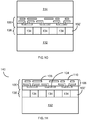
FIG. 1A illustrates an initial substrate that includes a device layer formed thereon; -
FIG. 1B illustrates a temporary substrate bonded to an exposed surface of the device layer opposite the initial substrate; -
FIG. 1C illustrates the thinning of a portion of the initial substrate; -
FIG. 1D illustrates forming a masking layer over the remaining portion of the initial substrate; -
FIG. 1E illustrates a plan view of the remaining portion of the initial substrate with the masking layer thereon; -
FIG. 1F illustrates forming a high resistivity layer by forming a plurality of vias through the remaining portion of the initial substrate;. -
FIG. 1G µillustrates attaching a final substrate to the high resistivity layer; and -
FIG. 1H illustrates removing the temporary substrate. -
FIGS. 2A through 2D are simplified, schematically illustrated cross-sectional views illustrating fabrication of semiconductor structures and devices that may be employed in accordance with an another embodiment of the present disclosure; -
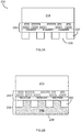
FIGS. 2A illustrates a semiconductor structure including a temporary substrate, a device layer and a remaining portion of an initial substrate including a plurality of vias; -
FIG. 2B illustrates forming a high resistivity layer by applying a high resistivity material over the plurality of vias. -
FIG. 2C attaching a final substrate to the high resistivity layer; and -
FIG. 2D illustrates removing the temporary substrate from the semiconductror structure ofFIG. 2C . - The illustrations presented herein are not meant to be actual views of any particular semiconductor structure, device, system, or method, but are merely idealized representations that are used to describe embodiments of the disclosure.
- Any headings used herein should not be considered to limit the scope of embodiments of the invention as defined by the claims below and their legal equivalents. Concepts described in any specific heading are generally applicable in other sections throughout the entire specification.
- An embodiment of the invention is described with reference to
FIGS. 1A through FIG. 1H . With reference toFIG. 1A embodiments may comprise forming adevice layer 100 on aninitial substrate 102. - In greater detail, the
device layer 100 may comprise a plurality ofelectronic devices 104, such electronic devices may comprise switching devices as well as further electronic device types such as, for example, logic, light emitting and light receiving devices. In certain embodiments the plurality ofelectronic devices 104 may comprise a plurality of radio frequency devices, such as RF CMOS devices. Thedevice layer 100 may also include aninterconnection layer 106 which may comprise electricallyconductive elements 108 disposed within an interlayer layerdielectric material 110. The plurality ofelectronic devices 104 may be formed on and / or in theinitial substrate 102 using standard electronic fabrication methods, as known in the art. - Embodiments may comprise selecting the
initial substrate 102 to comprise at least one of silicon, germanium, silicon germanium, silicon carbide, a III-V material or a II-VI material. Further embodiments may comprise selecting the initial substrate to exhibit a resistivity of between approximately about 5 Ohms-cm and about 30 Ohms-cm. Theinitial substrate 102 may also have a diameter depending on its final application of, for example, 300 mm, 200 mm or other diameters may be utilized. - The
device layer 100 may include an exposedsurface 112 and this exposedsurface 112 may be attached to atemporary substrate 114 to form asemiconductor structure 118, as illustrate inFIG.1B . Embodiments may comprise selecting thetemporary substrate 114 to comprise at least one of silicon, germanium, silicon germanium, silicon carbide, a III-V material or a II-VI material, glass, etc. In certain embodiments, theinitial substrate 102 and thetemporary substrate 114 may comprise essentially the same material. Such material matching of theinitial substrate 102 and thetemporary substrate 114 to one another may improve the processes for attaching thedevice layer 100 to thetemporary substrate 114. For example, the coefficient of thermal expansion of theinitial substrate 102 and the coefficient of thermal expansion of thetemporary substrate 114 may be selected to be essentially the same value to prevent unwanted stresses during the attachment processes. In further embodiments the difference between the coefficient of thermal expansion of theinitial substrate 102 and the coefficient of thermal expansion of thetemporary substrate 114 may be selected to be less than about 10 (ten) percent. - The attachment of the
device layer 100 to thetemporary substrate 114 may be preformed utilizing a bonding process. For example, the exposedsurface 112 of thedevice layer 100 may be bonded to asurface 116 oftemporary substrate 114. The bonding ofdevice layer 100 totemporary substrate 114 may be carried out by bonding to one another by a molecular adhesion process at room temperature (between approximately 20 °C and 30 °C, for example.) - As know in the art, the principle of bonding by molecular adhesion, called direct bonding, is based on the principle of bringing two surfaces (for example, the exposed
surface 112 of thedevice layer 100 andsurface 116 of the temporary substrate 114) into direct contact, i.e., without the use of a specific bonding material (adhesive, wax, solder, etc.). Such a bonding process requires that the surfaces to be bonded are sufficiently smooth and free of particles or contamination and that they are brought sufficiently close to make it possible to initiate contact, typically at a distance of less than a few nanometers. In this case, the attractive forces between the two surfaces are great enough to cause molecular adhesion (bonding induced by the sum of the attractive forces (van der Waals forces) of the electron interactions between the two atoms or molecules of the two surfaces to be bonded). - Bonding by molecular adhesion may be initiated by the application of a pressure point on at least one position of the semiconductor structure 118 (of
FIG. 1B ) formed by theinitial substrate 102, thedevice layer 100 and thetemporary substrate 114. The bonding wave between thetemporary substrate 114 and thedevice layer 100 is then propagated from the point where pressure was applied. The application of such a pressure is not, however, obligatory to initiate the propagation of the bonding wave. - After bonding by molecular adhesion, annealing may be carried on
semiconductor structure 118 out at a moderate temperature (preferably less than or equal to 100°C) in order to strengthen the bonding of thetemporary substrate 114 and thedevice layer 100. - In further embodiments, the bonding process for attaching
temporary substrate 114 to the exposedsurface 112 of thedevice layer 100 may be performed under compression at room temperature. In yet further embodiments, the bonding process may be performed under compression at a temperature of less than or equal to 100 °C. - In additional embodiments a bonding layer (not shown) may be disposed between the
temporary substrate 114 and thedevice layer 100. The bonding layer may be formed over one or both bonding surfaces of thedevice layer 100 and thetemporary substrate 114, i.e., on exposedsurfaces device layer 100 to thetemporary substrate 114. - Upon attaching the
temporary substrate 114 to thedevice layer 100 further processing may be utilized to form a high resistivity layer for improving RF performance of the plurality ofdevices 104 comprisingdevice layer 100. The formation of the high resistivity layer may comprise removing a portion of theinitial substrate 102 opposite thedevice layer 100. For example and with reference toFIG. 1C , a portion of theinitial substrate 102 opposite thedevice layer 100 may be removed by utilizing a thinning process to leave a remaining portion 102' of initial substrate102. The thinning of a portion of theinitial substrate 102 may comprise one or more of an etching, grinding and polishing process. For example, theinitial substrate 102 may have an initial thickness of approximately less than 1000 micron, or even less than 800 microns, or in certain embodiments even less than 500 microns. A thinning process may be utilized to remove a portion of the exposed back surface of theinitial substrate 102 thereby reducing the thickness of theinitial substrate 102 to less than approximately 100 microns, or less than 20 microns, or in certain embodiments even less than approximately 5 microns. - Upon thinning of a portion of the
initial substrate 102, amasking layer 122 may be formed over an exposed backsurface 120 of the remaining portion of the initial substrate 102' opposite thedevice layer 100, as illustrated inFIG. 1D . Themasking layer 122 may be formed over the exposed backsurface 120 of the remaining portion 102' of theinitial substrate 102 using methods well known in the semiconductor industry, such as standard photolithography methods. For example, themasking layer 122 may comprise one or more of a polymer, a silicon oxide, a silicon nitride, or a metallic layer. - As illustrate in
FIG. 1D themasking layer 122 comprises a plurality of maskingelements 124 and a plurality ofmask openings 126 disposed over theback surface 120 of the remaining portion 102' of theinitial substrate 102. An example embodiment of the layout of themasking layer 122 on theback surface 120 of the remaining portion 102' of theinitial substrate 102 is shown in plan view section inFIG. 1E . For example, as the illustrated example ofFIG. 1E shows the plurality of maskingelements 124, comprising themasking layer 122, may have a selected geometry such as rectangular, circular, or other suitable masking geometries. In some embodiments of the invention of the total surface area of the plurality of maskingelements 124 is less than seventy-five (75) percent of the total area of theback surface 120 of the remaining portion 102' of theinitial substrate 102, in other embodiments the total surface area of the plurality of maskingelements 124 is less than sixty (60) percent of the total area of theback surface 120 of the remaining portion 102' of theinitial substrate 102 or even in some embodiments the total surface area of the plurality of maskingelements 124 is less than fifty (50) percent of the total area of theback surface 120 of the remaining portion 102' of theinitial substrate 102. - Upon forming the
masking layer 122 an etching process may be performed to form a plurality ofvias 128 extending through the unmasked back surface of the remaining portion 102' ofinitial substrate 102 to formsemiconductor structure 130, as illustrate inFIG. 1F . For example, an etching process may comprise one or more of a dry etch process (such as a plasma etching process) or a wet etch process (such as wet acid etch). In certain embodiments of the invention the etching process may be performed until the plurality ofvias 128 are of a depth of approximately great than 5 microns, or greater than 20 microns, or even greater than 100 microns. The etching process is halted prior to impinging on thedevice layer 100 thereby preventing any unwanted damage to the plurality ofdevices 104 comprising thedevice layer 100. Upon completion of the etching process themasking layer 122 may be removed utilizing well known methods such as a chemical etch or a solvent clean. - After forming the plurality of
vias 128 extending through the remaining portion 102' of initial substrate 102 afinal substrate 132 may be attached over the plurality of vias forming a plurality ofcavities 134 between thefinal substrate 132 and thedevice layer 100, as illustrate inFIG. 1G , the plurality ofcavities 134 and the remaining portion 102' ofinitial substrate 102 forming ahigh resistivity layer 136. - In greater detail, embodiments of the invention may comprise selecting the
final substrate 132 to comprise at least one of silicon, germanium, silicon germanium, silicon carbide, a III-V material or a II-VI material. In additional embodiments thefinal substrate 132 may comprise one or more of a ceramic, a dielectric or an insulator. The final substrate may further comprise a single crystalline material or alternatively may comprise a poly-crystalline or amorphous material. Additional embodiments may comprise selecting thefinal substrate 132 to exhibit a resistivity of between approximately about 10 Ohms-cm and about 1,000,000 Ohms-cm. - The
final substrate 132 may be attached over the plurality ofvias 128 forming the plurality ofcavities 134 by making contact with the remaining portion 102' of theinitial substrate 102 using a bonding processes as previously described with reference to the bonding of thetemporary substrate 114 to thedevice layer 100. In addition, as described previously, a bonding layer (not shown) may be formed over one or more of thefinal substrate 132 and the remaining portion 102' of theinitial substrate 102 in order to improve the bonding process, for example by molecular bonding as previous described in detail above. - The attachment of the
final substrate 132 over the plurality ofvias 128 extending through the remaining portion 102' of theinitial substrate 102 forms ahigh resistivity layer 136, theresistivity layer 136 being disposed between thefinal substrate 132 and thedevice layer 100. Thehigh resistivity layer 136 therefore comprises a plurality ofcavities 134 and the remaining portion 102' of theinitial substrate 102. In certain embodiments the attachment of thefinal substrate 132 over the plurality ofvias 128 may be performed by a molecular bonding process such that the plurality ofcavities 134 comprise a plurality of air gaps essentially comprising atmospheric air. In further embodiments of the invention a molecular bonding process may be utilized under differing gaseous atmospheres such that the plurality ofcavities 134 may be filled with an atmosphere of choice and various gas pressures inside the cavities. - The
high resistivity layer 136 may be fabricated such that thehigh resistivity layer 136 has an average electrical resistivity of greater than approximately 10000 Ohms-cm, or greater than approximately 100000 Ohms-cm, or even greater than 1000000 Ohms-cm. The fabrication of thehigh resistivity layer 136 disposed between thefinal substrate 132 and thedevice layer 100 ensures optimal performance of RF devices fabricated within thedevice layer 100. - Upon fabrication of the
high resistivity layer 136 embodiments of the invention may proceed by the removal of thetemporary substrate 114 as illustrate inFIG. 1H . Thetemporary substrate 114 may be removed by one or more of an etching, grinding, or polishing process. The removal process of thetemporary substrate 114 is performed until the entiretemporary substrate 114 has been removed thereby re-exposing thedevice layer 100 and particularly exposing theinterconnection layer 106 comprising theinterlayer dielectric 110 and conductingelements 106. - The embodiments of the invention as described above teach methods and structures for forming a high resistivity layer comprising a remaining portion of the initial substrate and a plurality of cavities. In additional embodiments of the invention described below the high resistivity layer may comprise a remaining portion of the initial substrate as well as an additional high resistivity material formed there over.
- In further detail and with reference to
FIG. 2A , asemiconductor structure 230 is formed and comprises atemporary substrate 214, adevice 200, a remaining portion 202' of an initial substrate and a plurality ofvias 228 extending through the remaining portion 202' of the initial substrate. Thesemiconductor structure 230 inFIG. 2A is essentially the same semiconductor structure assemiconductor structure 130 ofFIG. 1F and may be formed using essentially the same methods as those previously described above in the formation ofsemiconductor structure 130 ofFIG. 1F . - Having fabricated
semiconductor structure 230 ofFIG. 2A embodiments may proceed by the formation of ahigh resistivity layer 236 comprising the remaining portion 202' of the initial substrate and an additionalhigh resistivity material 238. In some embodiments of the invention, thehigh resistivity material 238 may be disposed over the remaining portion 202' of the initial substrate and may also fill the plurality ofvias 228, as illustrated inFIG. 2B . - A number of processes may be utilized for the formation of the
high resistivity material 238, for example, one or more of a deposition process (for example, chemical vapor deposition, physical vapor deposition etc.) or a spin-on process may utilized in the formation of thehigh resistivity material 238. Thehigh resistivity material 238 may be formed utilizing a conformal formation processes and subsequent planarized to form the exposed planarhigh resistivity surface 239. The planarization process for forminghigh resistivity surface 239 may be performed utilizing one or more of chemical polishing, grinding or etching process. - In some embodiment of the invention the
high resistivity material 238 may comprise one or more of dielectric materials, such as, for example, silicon oxide, silicon nitride, high resistivity polymers, polyimide, or a ceramic glue. Thehigh resistivity material 238 may comprise a high resistivity material with an electrical resistivity value of great than approximately 10000 Ohms-cm, or greater than approximately 100000 Ohms-cm, or even greater than 1000000 Ohms-cm. - Upon formation of the high resistivity layer 236 a
final substrate 232 may be attached to thehigh resistivity layer 236, as illustrate inFIG 2C . The attachment of thehigh resistivity layer 236 to thefinal substrate 232 may be performed utilizing a bonding process as previously described with reference to the bonding of thetemporary substrate 114 to thedevice layer 100. In addition as described previously, a bonding layer (not shown) may formed over one or more of thefinal substrate 232 and thehigh resistivity layer 236 in order to improve the bonding process, for example by molecular bonding as previous described in detail above. - Upon fabrication of the
high resistivity layer 236 embodiments of the invention may proceed by the removal of thetemporary substrate 214 as illustrate inFIG. 2D . Thetemporary substrate 214 may be removed by one or more of an etching, grinding, or polishing process. The removal process of thetemporary substrate 214 is performed until the entiretemporary substrate 214 has been removed thereby re-exposing thedevice layer 200 and particularly exposing the interconnection layer comprising the interlayer dielectric and conducting elements. - According to a first exemplary implementation (described with reference to
figures 1A to 1H ), adevice layer 100 comprising RF switches is produced on aninitial substrate 102 made of silicon, with a resistivity of 5 ohm.cm, a diameter of 300 mm and a thickness of 800 microns (figure 1A ). - A
temporary substrate 114 made of silicon, with a diameter of 300 mm and a thickness of 800 microns is assembled by molecular adhesion bonding to the exposed surface of thedevice layer 100. Prior to the bonding, the exposed surface of the layer ofdevices 100 may have undergone chemical mechanical planarization followed by cleaning in order to give the surface the flatness, low level of roughness and cleanliness required with a view to bonding by molecular adhesion. Thetemporary substrate 114 may in turn have also undergone microelectronic cleaning (for instance, by ozone + RCA) in order to provide it the proper surface properties. An assembled semiconductor structure 118 (figure 1B ) is thus obtained. The rear side of the initial substrate 102 (i.e. the side opposite that bearing the layer of devices 100) is subsequently thinned, for example by mechanical grinding and subsequently by chemical mechanical polishing until a residual thickness of 5 microns is achieved (figure 1C ). Prior to the thinning stage, the assembledsemiconductor structure 118 may undergo heat treatment, at around 100-150°C for example, in order to enhance the bonding forces at the interface between thetemporary substrate 114 and thedevice layer 100. - A photolithography stage subsequently serves to apply to the thinned rear side of the
initial substrate 102, amasking layer 122, definingmasked areas 124 and unmasked areas 126 (figures 1D and IE). By way of example, themasked areas 124 are squares with side dimensions of 10 x 20 microns. The surface area of themasked areas 124 is less than 50% of the total surface area of the thinned side of theinitial substrate 102, i.e. 40% for example. A chemical etching stage is subsequently used to etch the unmaskedareas 126 of theinitial substrate 102, in order to form vias 128 (figure 1F ). Themasking layer 122 is removed. - A
final substrate 132 consisting of aluminum nitride, of a thickness of 500 microns for example, is subsequently prepared with a view to its assembly on the thinned rear side of theinitial substrate 102. Preparation of the surfaces to be assembled may comprise plasma treatment (under oxygen or nitrogen) capable of activating the surfaces and of providing the subsequent bonding high adhesion energy at low temperatures. Assembly is performed using a direct bonding technique, under controlled atmosphere. By way of example, the atmosphere of the bonding chamber may be air at atmospheric pressure or a gas (for example nitrogen or argon, or another gas) at a selected pressure. Following assembly (figure 1G ), the high-resistivity layer 136 is formed: it consists of a remaining portion 102' of theinitial substrate 102 andcavities 134, filled with air or a selected gas, at a chosen pressure. Low-temperature heat treatment (on the order of 100°C, given the major difference between the thermal expansion coefficients of the assembled temporary and final substrates) may be performed in order to enhance the bonding energy between the thinned side of theinitial substrate 102 and thefinal substrate 132. - The last stage involves removal of the
temporary substrate 114. It can be performed either by removing the latter by mechanical grinding and chemical etching, or preferentially by disassembly, i.e. by applying mechanical stress at the bonding interface between thetemporary substrate 114 and thedevice layer 100. - The
structure 140 thus obtained gives good RF performances to the switches included in the layer ofdevices 100 owing to the presence of a final substrate with electrical insulation properties more favorable than those of theinitial substrate 102; furthermore, the remaining portion 102' of theinitial substrate 102 does not impair the performances of the devices by creating a conduction path owing to formation of the high-resistivity layer 136. - The manufacturing technique according to the invention thus makes it possible to use an initial silicon substrate, instead of an SOI substrate, which is more expensive and following a double transfer of layer and manufacture of the high-
resistivity layer 136, to obtain a structure the properties of which are suitable for RF applications. - According to a second exemplary implementation (described with reference to
figures 2A to 2D ), adevice layer 200 comprising RF switches is produced on an initial substrate made of silicon, with a resistance of 30 ohm.cm, a diameter of 300 mm and a thickness of 800 microns. Atemporary substrate 214 made of silicon, with a diameter of 300 mm and a thickness of 800 microns is assembled by direct bonding to the exposed surface of the layer ofdevices 200. Prior to the bonding, the exposed surface of thedevice layer 200 may have undergone chemical mechanical planarization followed by cleaning in order to give the surface the flatness, low level of roughness and cleanliness required with a view to bonding by molecular adhesion. Thetemporary substrate 214 may in turn have also undergone microelectronic cleaning (for instance, by ozone + RCA) in order to provide it the correct surface properties. The rear side of the initial substrate (i.e. the side opposite that bearing the layer of devices 200) is subsequently thinned, for example by mechanical grinding and subsequently by chemical mechanical polishing until a residual thickness of 20 microns is achieved. - A photolithography stage subsequently serves to apply to the thinned rear side (remaining portion 202') of the initial substrate, a masking layer, defining masked areas and unmasked areas. By way of example, the masked areas are rectangles with side dimensions of 10 x 20 microns. The surface area of the masked areas is less than 75% of the total surface area of the thinned side of the
initial substrate 202, i.e. 55% for example. A chemical etching stage is subsequently used to etch the unmasked areas of the remaining portion 202' of the initial substrate, in order to form vias 228 (figure 2A ). The masking layer is removed. - A layer of high-
resistivity material 238 is subsequently deposited in thevias 228, so as to fill the latter (i.e. a thickness at least equal to the residual thickness of the remaining portion 202' of the initial substrate) and if appropriate, on the remaining portion 202' of the initial substrate (as illustrated infigure 2B ). This high-resistivity material will for example be silicon oxide or alternatively, it may be made of high-resistivity (i.e. preferably greater than 10,000 Ohm.cm) polymer. It will subsequently be possible to prepare the exposedsurface 239 of the high-resistivity material 238 with a view to direct bonding, for example by application of chemical mechanical planarization followed by RCA cleaning. - A
final substrate 232 made of glass, of a thickness of 500 microns for example, is subsequently prepared with a view to its assembly on the thinned rear side of the initial substrate (remaining portion 202'). Preparation of the surfaces to be assembled may comprise plasma treatment (under oxygen or nitrogen) capable of activating the surfaces and of providing the subsequent bonding high adhesion energy at low temperatures. Assembly is performed using a direct bonding technique. Following assembly (figure 2C ), the high-resistivity layer 236 is formed: it consists of the remaining portion 202' of the initial substrate and the high-resistivity material 238. Low-temperature heat treatment (on the order of 100°C, given the major difference between the thermal expansion coefficients of the assembled temporary and final substrates) may be performed in order to enhance the bonding energy between the thinned side of the initial substrate and thefinal substrate 232. - The last stage involves removal of the temporary substrate 214 (
figure 2D ). It can be performed either by removing the latter by mechanical grinding and chemical etching, or preferentially by debonding, i.e. by applying mechanical stress for example at the bonding interface between thetemporary substrate 214 and the layer ofdevices 200. - The
semiconductor structure 240 thus obtained gives good RF performances to the switches included in thedevice layer 200 owing to the presence of afinal substrate 232 with electrical insulation properties more favorable than those of the initial substrate; furthermore, the residual thickness of the remaining portion 202' of the initial substrate does not impair the performances of the devices by creating a conduction path owing to formation of the high-resistivity layer 136. - The example embodiments of the disclosure described above do not limit the scope of the invention, since these embodiments are merely examples of embodiments of the invention, which is defined by the scope of the appended claims and their legal equivalents. Any equivalent embodiments are intended to be within the scope of this invention. Indeed, various modifications of the disclosure, in addition to those shown and described herein, such as alternate useful combinations of the elements described, will become apparent to those skilled in the art from the description. In other words, one or more features of one example embodiment described herein may be combined with one or more features of another example embodiment described herein to provide additional embodiments of the disclosure. Such modifications and embodiments are also intended to fall within the scope of the appended claims.
Claims (15)
- A method of forming a semiconductor structure (140, 240) comprising:forming a device layer (100, 200) on an initial substrate (102);attaching a first surface of the device layer (100, 200) to a temporary substrate (114, 214);forming a high resistivity layer (136, 236), wherein forming the high resistivity layer comprises removing a portion of the initial substrate (102), the high resistivity layer comprising a remaining portion (102', 202') of the initial substrate;attaching a final substrate (132, 232) to the high resistivity layer (136, 236); andremoving the temporary substrate (114, 214).
- The method of claim 1 wherein removing a portion of the initial substrate (102) comprises thinning a portion of the initial substrate (102).
- The method of claim 2 wherein removing a portion of the initial substrate (102) further comprises forming a plurality of vias (128, 228) extending through a remaining portion (102', 202') of the initial substrate (102).
- The method of claim 3 wherein forming a plurality of vias (128, 228) through a remaining portion (102', 202') of the initial substrate (102) further comprises;
forming a masking layer (124) over an exposed surface (120) of the remaining portion (102') of the initial substrate (102), and
etching vias (128) through the unmasked remaining portion (126) of the initial substrate (102). - The method of claim 4 wherein the masking layer (124) comprises a plurality of masking elements and further comprising selecting the total surface area of the plurality of masking elements to be less than seventy-five (75) percent of the total surface area of the exposed surface (120) of the remaining portion (102') of the initial substrate (102).
- The method as claimed in any of claims 3 to 5 wherein attaching the final substrate (132) to the high resistivity layer (136) comprises attaching the final substrate (132) to the plurality of vias (128) forming a plurality of cavities (134) between the final substrate (132) and the device layer (100).
- The method as claimed in any of claims 3 to 5 further comprising forming a high resistivity material (238) over the plurality of vias (128, 228).
- The method of claim 7 further comprising selecting the high resistivity material (238) to have an electrical resistivity great than 10,000 Ohm.cm.
- The method of claim 7 further comprising selecting the high resistivity material (238) to comprise at least one of a silicon oxide, a silicon nitride, a high resistivity polymers, a polyimide, or a ceramic glue.
- A semiconductor structure (140, 240) comprising:a final substrate (132, 232);a high resistivity layer (136, 236) disposed over the final substrate (132, 232); the high resistivity layer (136, 236) comprising : a remaining portion (102', 202') of an initial substrate (102),and a plurality of vias (128, 228) extending through said remaining portion (102', 202'),and a radio frequency electronic device layer (100, 200) disposed over the high resistivity layer (136, 236).
- The semiconductor structure (140, 240) of claim 10 wherein the high resistivity layer (136, 236) comprises a layer with an average electrical resistance of greater than approximately 10000 Ohm.cm
- The semiconductor structure (140) as claimed in any of claims 10 to 11 wherein the high resistivity layer (136) comprises a remaining portion (102') of the initial substrate (102) and a plurality of cavities (134).
- The semiconductor structure (240) as claimed in any of claims 10 to 11 wherein the high resistivity layer (236) further comprises a high resistivity material (238) disposed between the plurality of vias (228).
- The semiconductor structure (240) of claim 13 wherein the high resistivity material (238) comprises one or more of a silicon oxide, a silicon nitride, a high resistivity polymers, a polyimide, or a ceramic glue.
- The semiconductor structure (240) of claim 13 wherein the high resistivity material (238) has a electrical resistivity great than approximately 10000 Ohm.cm.
Applications Claiming Priority (1)
| Application Number | Priority Date | Filing Date | Title |
|---|---|---|---|
| FR1650333A FR3046874B1 (en) | 2016-01-15 | 2016-01-15 | METHOD FOR MANUFACTURING SEMICONDUCTOR STRUCTURES INCLUDING A HIGH RESISTIVITY LAYER, AND RELATED SEMICONDUCTOR STRUCTURES |
Publications (2)
| Publication Number | Publication Date |
|---|---|
| EP3193361A1 true EP3193361A1 (en) | 2017-07-19 |
| EP3193361B1 EP3193361B1 (en) | 2023-04-12 |
Family
ID=55759798
Family Applications (1)
| Application Number | Title | Priority Date | Filing Date |
|---|---|---|---|
| EP17150341.0A Active EP3193361B1 (en) | 2016-01-15 | 2017-01-05 | Method for fabricating semiconductor structures including a high resistivity layer, and related semiconductor structures |
Country Status (9)
| Country | Link |
|---|---|
| US (1) | US10276492B2 (en) |
| EP (1) | EP3193361B1 (en) |
| JP (3) | JP2017126749A (en) |
| KR (1) | KR102714466B1 (en) |
| CN (1) | CN107068571B (en) |
| FI (1) | FI3193361T3 (en) |
| FR (1) | FR3046874B1 (en) |
| SG (1) | SG10201700308QA (en) |
| TW (1) | TWI720105B (en) |
Families Citing this family (5)
| Publication number | Priority date | Publication date | Assignee | Title |
|---|---|---|---|---|
| CN111430217B (en) * | 2019-01-09 | 2022-11-29 | 芯恩(青岛)集成电路有限公司 | Semiconductor device and manufacturing method thereof |
| EP3772749A1 (en) | 2019-08-08 | 2021-02-10 | Infineon Technologies Dresden GmbH & Co . KG | Methods and devices related to radio frequency devices |
| US11509949B2 (en) | 2019-09-13 | 2022-11-22 | Disney Enterprises, Inc. | Packager for segmenter fluidity |
| US11728199B2 (en) * | 2019-12-23 | 2023-08-15 | Asmpt Nexx, Inc. | Substrate support features and method of application |
| FR3108439B1 (en) * | 2020-03-23 | 2022-02-11 | Soitec Silicon On Insulator | PROCESS FOR MANUFACTURING A STACKED STRUCTURE |
Citations (2)
| Publication number | Priority date | Publication date | Assignee | Title |
|---|---|---|---|---|
| US20030203547A1 (en) * | 1996-12-18 | 2003-10-30 | Kiyofumi Sakaguchi | Process for producing semiconductor article |
| FR2993398A1 (en) * | 2012-07-11 | 2014-01-17 | Soitec Silicon On Insulator | Method for manufacturing semiconductor structure used in microelectronic application, involves connecting semiconductor material to substrate by establishing molecular connections and defining micro-channel between dielectric materials |
Family Cites Families (14)
| Publication number | Priority date | Publication date | Assignee | Title |
|---|---|---|---|---|
| JPS6154674A (en) * | 1984-08-25 | 1986-03-18 | Fujitsu Ltd | Super-high frequency integrated circuit device |
| US6162665A (en) * | 1993-10-15 | 2000-12-19 | Ixys Corporation | High voltage transistors and thyristors |
| JP4034099B2 (en) * | 2002-03-28 | 2008-01-16 | 株式会社ルネサステクノロジ | High frequency monolithic integrated circuit device and method of manufacturing the same |
| CN1856873A (en) * | 2003-09-26 | 2006-11-01 | 卢万天主教大学 | Method of manufacturing a multilayer semiconductor structure with reduced ohmic losses |
| JP5230061B2 (en) * | 2005-07-25 | 2013-07-10 | ラピスセミコンダクタ株式会社 | Semiconductor device and manufacturing method thereof |
| JP5367323B2 (en) * | 2008-07-23 | 2013-12-11 | ラピスセミコンダクタ株式会社 | Semiconductor device and manufacturing method of semiconductor device |
| US9064712B2 (en) * | 2010-08-12 | 2015-06-23 | Freescale Semiconductor Inc. | Monolithic microwave integrated circuit |
| JP2012156403A (en) * | 2011-01-27 | 2012-08-16 | Panasonic Corp | Glass-embedded silicon substrate, and method of manufacturing the same |
| CN102183335B (en) * | 2011-03-15 | 2015-10-21 | 迈尔森电子(天津)有限公司 | MEMS pressure sensor and preparation method thereof |
| US8934021B2 (en) * | 2012-07-02 | 2015-01-13 | Dayton D. Eden | Dual-mode terahertz imaging systems |
| US9116244B1 (en) * | 2013-02-28 | 2015-08-25 | Rockwell Collins, Inc. | System for and method of weather phenomenon detection using multiple beams |
| CN104681562B (en) * | 2013-11-28 | 2017-11-14 | 中芯国际集成电路制造(上海)有限公司 | A kind of integrated circuit and its manufacture method and electronic installation |
| US20150371905A1 (en) * | 2014-06-20 | 2015-12-24 | Rf Micro Devices, Inc. | Soi with gold-doped handle wafer |
| US9475692B2 (en) * | 2014-07-22 | 2016-10-25 | Qorvo Us, Inc. | Radio frequency (RF) microelectromechanical systems (MEMS) devices with gold-doped silicon |
-
2016
- 2016-01-15 FR FR1650333A patent/FR3046874B1/en active Active
-
2017
- 2017-01-05 EP EP17150341.0A patent/EP3193361B1/en active Active
- 2017-01-05 TW TW106100242A patent/TWI720105B/en active
- 2017-01-05 FI FIEP17150341.0T patent/FI3193361T3/en active
- 2017-01-12 CN CN201710022513.6A patent/CN107068571B/en active Active
- 2017-01-12 JP JP2017003284A patent/JP2017126749A/en active Pending
- 2017-01-13 US US15/405,867 patent/US10276492B2/en active Active
- 2017-01-13 SG SG10201700308QA patent/SG10201700308QA/en unknown
- 2017-01-13 KR KR1020170006120A patent/KR102714466B1/en active Active
-
2021
- 2021-07-30 JP JP2021125773A patent/JP2021168426A/en active Pending
-
2023
- 2023-06-21 JP JP2023101912A patent/JP7578762B2/en active Active
Patent Citations (2)
| Publication number | Priority date | Publication date | Assignee | Title |
|---|---|---|---|---|
| US20030203547A1 (en) * | 1996-12-18 | 2003-10-30 | Kiyofumi Sakaguchi | Process for producing semiconductor article |
| FR2993398A1 (en) * | 2012-07-11 | 2014-01-17 | Soitec Silicon On Insulator | Method for manufacturing semiconductor structure used in microelectronic application, involves connecting semiconductor material to substrate by establishing molecular connections and defining micro-channel between dielectric materials |
Also Published As
| Publication number | Publication date |
|---|---|
| FR3046874A1 (en) | 2017-07-21 |
| FR3046874B1 (en) | 2018-04-13 |
| CN107068571B (en) | 2021-09-10 |
| JP7578762B2 (en) | 2024-11-06 |
| US20170207164A1 (en) | 2017-07-20 |
| CN107068571A (en) | 2017-08-18 |
| EP3193361B1 (en) | 2023-04-12 |
| TW201735257A (en) | 2017-10-01 |
| SG10201700308QA (en) | 2017-08-30 |
| KR102714466B1 (en) | 2024-10-10 |
| JP2021168426A (en) | 2021-10-21 |
| US10276492B2 (en) | 2019-04-30 |
| FI3193361T3 (en) | 2023-05-09 |
| JP2017126749A (en) | 2017-07-20 |
| KR20170085981A (en) | 2017-07-25 |
| TWI720105B (en) | 2021-03-01 |
| JP2023112087A (en) | 2023-08-10 |
Similar Documents
| Publication | Publication Date | Title |
|---|---|---|
| JP7578762B2 (en) | Method for fabricating a semiconductor structure including a high resistivity layer, and related semiconductor structure - Patents.com | |
| US7166520B1 (en) | Thin handle substrate method and structure for fabricating devices using one or more films provided by a layer transfer process | |
| KR101876912B1 (en) | Electronic device for radiofrequency or power applications and process for manufacturing such a device | |
| KR101292111B1 (en) | A method of producing a heterostructure with local adaptation of the thermal expansion coefficient | |
| US6911375B2 (en) | Method of fabricating silicon devices on sapphire with wafer bonding at low temperature | |
| US20100155882A1 (en) | Method for bonding two substrates | |
| CN105340070B (en) | Method for joining metal contact surfaces | |
| US20110076849A1 (en) | Process for bonding and transferring a layer | |
| EP0996150A1 (en) | Method of manufacturing passive and active devices on the same insulated substrate | |
| JP2015502655A (en) | Silicon-on-insulator material and method of manufacturing the same | |
| US20140240944A1 (en) | Insulating low signal loss substrate, integrated circuits including a non-silicon substrate and methods of manufacture of integrated circuits | |
| KR20120117843A (en) | Method for the preparation of a multi-layered crystalline structure | |
| US8298915B2 (en) | Method of transferring a circuit onto a ground plane | |
| JP2023519166A (en) | Method for manufacturing laminated structure | |
| KR100751619B1 (en) | Production of a Structure Comprising a Protective Layer against Chemical Treatments | |
| CN112701128B (en) | SON structure and preparation method thereof | |
| JP7041648B2 (en) | Manufacturing method of composite substrate | |
| KR101969679B1 (en) | Method for forming and transferring thin film using soi wafer and thermal process | |
| KR102568640B1 (en) | Method for producing the remainder of the donor substrate, substrate produced by the method and use of the substrate | |
| CN117153769A (en) | SOI substrate and preparation method thereof | |
| CN121398562A (en) | Preparation method of SOI chip structure and SOI chip structure | |
| KR20200124623A (en) | Method and structure for low density silicon oxide for fusion bonding and debonding |
Legal Events
| Date | Code | Title | Description |
|---|---|---|---|
| PUAI | Public reference made under article 153(3) epc to a published international application that has entered the european phase |
Free format text: ORIGINAL CODE: 0009012 |
|
| STAA | Information on the status of an ep patent application or granted ep patent |
Free format text: STATUS: REQUEST FOR EXAMINATION WAS MADE |
|
| 17P | Request for examination filed |
Effective date: 20170105 |
|
| AK | Designated contracting states |
Kind code of ref document: A1 Designated state(s): AL AT BE BG CH CY CZ DE DK EE ES FI FR GB GR HR HU IE IS IT LI LT LU LV MC MK MT NL NO PL PT RO RS SE SI SK SM TR |
|
| AX | Request for extension of the european patent |
Extension state: BA ME |
|
| STAA | Information on the status of an ep patent application or granted ep patent |
Free format text: STATUS: EXAMINATION IS IN PROGRESS |
|
| 17Q | First examination report despatched |
Effective date: 20210223 |
|
| GRAJ | Information related to disapproval of communication of intention to grant by the applicant or resumption of examination proceedings by the epo deleted |
Free format text: ORIGINAL CODE: EPIDOSDIGR1 |
|
| GRAP | Despatch of communication of intention to grant a patent |
Free format text: ORIGINAL CODE: EPIDOSNIGR1 |
|
| GRAP | Despatch of communication of intention to grant a patent |
Free format text: ORIGINAL CODE: EPIDOSNIGR1 |
|
| STAA | Information on the status of an ep patent application or granted ep patent |
Free format text: STATUS: GRANT OF PATENT IS INTENDED |
|
| RAP3 | Party data changed (applicant data changed or rights of an application transferred) |
Owner name: SOITEC |
|
| INTG | Intention to grant announced |
Effective date: 20230113 |
|
| GRAS | Grant fee paid |
Free format text: ORIGINAL CODE: EPIDOSNIGR3 |
|
| GRAA | (expected) grant |
Free format text: ORIGINAL CODE: 0009210 |
|
| STAA | Information on the status of an ep patent application or granted ep patent |
Free format text: STATUS: THE PATENT HAS BEEN GRANTED |
|
| AK | Designated contracting states |
Kind code of ref document: B1 Designated state(s): AL AT BE BG CH CY CZ DE DK EE ES FI FR GB GR HR HU IE IS IT LI LT LU LV MC MK MT NL NO PL PT RO RS SE SI SK SM TR |
|
| REG | Reference to a national code |
Ref country code: GB Ref legal event code: FG4D |
|
| REG | Reference to a national code |
Ref country code: CH Ref legal event code: EP |
|
| REG | Reference to a national code |
Ref country code: DE Ref legal event code: R096 Ref document number: 602017067622 Country of ref document: DE |
|
| REG | Reference to a national code |
Ref country code: IE Ref legal event code: FG4D |
|
| REG | Reference to a national code |
Ref country code: AT Ref legal event code: REF Ref document number: 1560261 Country of ref document: AT Kind code of ref document: T Effective date: 20230515 |
|
| REG | Reference to a national code |
Ref country code: LT Ref legal event code: MG9D |
|
| REG | Reference to a national code |
Ref country code: NL Ref legal event code: MP Effective date: 20230412 |
|
| REG | Reference to a national code |
Ref country code: AT Ref legal event code: MK05 Ref document number: 1560261 Country of ref document: AT Kind code of ref document: T Effective date: 20230412 |
|
| PG25 | Lapsed in a contracting state [announced via postgrant information from national office to epo] |
Ref country code: NL Free format text: LAPSE BECAUSE OF FAILURE TO SUBMIT A TRANSLATION OF THE DESCRIPTION OR TO PAY THE FEE WITHIN THE PRESCRIBED TIME-LIMIT Effective date: 20230412 |
|
| PG25 | Lapsed in a contracting state [announced via postgrant information from national office to epo] |
Ref country code: SE Free format text: LAPSE BECAUSE OF FAILURE TO SUBMIT A TRANSLATION OF THE DESCRIPTION OR TO PAY THE FEE WITHIN THE PRESCRIBED TIME-LIMIT Effective date: 20230412 Ref country code: PT Free format text: LAPSE BECAUSE OF FAILURE TO SUBMIT A TRANSLATION OF THE DESCRIPTION OR TO PAY THE FEE WITHIN THE PRESCRIBED TIME-LIMIT Effective date: 20230814 Ref country code: NO Free format text: LAPSE BECAUSE OF FAILURE TO SUBMIT A TRANSLATION OF THE DESCRIPTION OR TO PAY THE FEE WITHIN THE PRESCRIBED TIME-LIMIT Effective date: 20230712 Ref country code: ES Free format text: LAPSE BECAUSE OF FAILURE TO SUBMIT A TRANSLATION OF THE DESCRIPTION OR TO PAY THE FEE WITHIN THE PRESCRIBED TIME-LIMIT Effective date: 20230412 Ref country code: AT Free format text: LAPSE BECAUSE OF FAILURE TO SUBMIT A TRANSLATION OF THE DESCRIPTION OR TO PAY THE FEE WITHIN THE PRESCRIBED TIME-LIMIT Effective date: 20230412 |
|
| PG25 | Lapsed in a contracting state [announced via postgrant information from national office to epo] |
Ref country code: RS Free format text: LAPSE BECAUSE OF FAILURE TO SUBMIT A TRANSLATION OF THE DESCRIPTION OR TO PAY THE FEE WITHIN THE PRESCRIBED TIME-LIMIT Effective date: 20230412 Ref country code: PL Free format text: LAPSE BECAUSE OF FAILURE TO SUBMIT A TRANSLATION OF THE DESCRIPTION OR TO PAY THE FEE WITHIN THE PRESCRIBED TIME-LIMIT Effective date: 20230412 Ref country code: LV Free format text: LAPSE BECAUSE OF FAILURE TO SUBMIT A TRANSLATION OF THE DESCRIPTION OR TO PAY THE FEE WITHIN THE PRESCRIBED TIME-LIMIT Effective date: 20230412 Ref country code: LT Free format text: LAPSE BECAUSE OF FAILURE TO SUBMIT A TRANSLATION OF THE DESCRIPTION OR TO PAY THE FEE WITHIN THE PRESCRIBED TIME-LIMIT Effective date: 20230412 Ref country code: IS Free format text: LAPSE BECAUSE OF FAILURE TO SUBMIT A TRANSLATION OF THE DESCRIPTION OR TO PAY THE FEE WITHIN THE PRESCRIBED TIME-LIMIT Effective date: 20230812 Ref country code: HR Free format text: LAPSE BECAUSE OF FAILURE TO SUBMIT A TRANSLATION OF THE DESCRIPTION OR TO PAY THE FEE WITHIN THE PRESCRIBED TIME-LIMIT Effective date: 20230412 Ref country code: GR Free format text: LAPSE BECAUSE OF FAILURE TO SUBMIT A TRANSLATION OF THE DESCRIPTION OR TO PAY THE FEE WITHIN THE PRESCRIBED TIME-LIMIT Effective date: 20230713 Ref country code: AL Free format text: LAPSE BECAUSE OF FAILURE TO SUBMIT A TRANSLATION OF THE DESCRIPTION OR TO PAY THE FEE WITHIN THE PRESCRIBED TIME-LIMIT Effective date: 20230412 |
|
| REG | Reference to a national code |
Ref country code: DE Ref legal event code: R097 Ref document number: 602017067622 Country of ref document: DE |
|
| PG25 | Lapsed in a contracting state [announced via postgrant information from national office to epo] |
Ref country code: SK Free format text: LAPSE BECAUSE OF FAILURE TO SUBMIT A TRANSLATION OF THE DESCRIPTION OR TO PAY THE FEE WITHIN THE PRESCRIBED TIME-LIMIT Effective date: 20230412 |
|
| PG25 | Lapsed in a contracting state [announced via postgrant information from national office to epo] |
Ref country code: SM Free format text: LAPSE BECAUSE OF FAILURE TO SUBMIT A TRANSLATION OF THE DESCRIPTION OR TO PAY THE FEE WITHIN THE PRESCRIBED TIME-LIMIT Effective date: 20230412 Ref country code: SK Free format text: LAPSE BECAUSE OF FAILURE TO SUBMIT A TRANSLATION OF THE DESCRIPTION OR TO PAY THE FEE WITHIN THE PRESCRIBED TIME-LIMIT Effective date: 20230412 Ref country code: RO Free format text: LAPSE BECAUSE OF FAILURE TO SUBMIT A TRANSLATION OF THE DESCRIPTION OR TO PAY THE FEE WITHIN THE PRESCRIBED TIME-LIMIT Effective date: 20230412 Ref country code: EE Free format text: LAPSE BECAUSE OF FAILURE TO SUBMIT A TRANSLATION OF THE DESCRIPTION OR TO PAY THE FEE WITHIN THE PRESCRIBED TIME-LIMIT Effective date: 20230412 Ref country code: DK Free format text: LAPSE BECAUSE OF FAILURE TO SUBMIT A TRANSLATION OF THE DESCRIPTION OR TO PAY THE FEE WITHIN THE PRESCRIBED TIME-LIMIT Effective date: 20230412 Ref country code: CZ Free format text: LAPSE BECAUSE OF FAILURE TO SUBMIT A TRANSLATION OF THE DESCRIPTION OR TO PAY THE FEE WITHIN THE PRESCRIBED TIME-LIMIT Effective date: 20230412 |
|
| PLBE | No opposition filed within time limit |
Free format text: ORIGINAL CODE: 0009261 |
|
| STAA | Information on the status of an ep patent application or granted ep patent |
Free format text: STATUS: NO OPPOSITION FILED WITHIN TIME LIMIT |
|
| 26N | No opposition filed |
Effective date: 20240115 |
|
| PG25 | Lapsed in a contracting state [announced via postgrant information from national office to epo] |
Ref country code: SI Free format text: LAPSE BECAUSE OF FAILURE TO SUBMIT A TRANSLATION OF THE DESCRIPTION OR TO PAY THE FEE WITHIN THE PRESCRIBED TIME-LIMIT Effective date: 20230412 |
|
| PG25 | Lapsed in a contracting state [announced via postgrant information from national office to epo] |
Ref country code: SI Free format text: LAPSE BECAUSE OF FAILURE TO SUBMIT A TRANSLATION OF THE DESCRIPTION OR TO PAY THE FEE WITHIN THE PRESCRIBED TIME-LIMIT Effective date: 20230412 Ref country code: IT Free format text: LAPSE BECAUSE OF FAILURE TO SUBMIT A TRANSLATION OF THE DESCRIPTION OR TO PAY THE FEE WITHIN THE PRESCRIBED TIME-LIMIT Effective date: 20230412 |
|
| PG25 | Lapsed in a contracting state [announced via postgrant information from national office to epo] |
Ref country code: MC Free format text: LAPSE BECAUSE OF FAILURE TO SUBMIT A TRANSLATION OF THE DESCRIPTION OR TO PAY THE FEE WITHIN THE PRESCRIBED TIME-LIMIT Effective date: 20230412 |
|
| PG25 | Lapsed in a contracting state [announced via postgrant information from national office to epo] |
Ref country code: MC Free format text: LAPSE BECAUSE OF FAILURE TO SUBMIT A TRANSLATION OF THE DESCRIPTION OR TO PAY THE FEE WITHIN THE PRESCRIBED TIME-LIMIT Effective date: 20230412 |
|
| REG | Reference to a national code |
Ref country code: CH Ref legal event code: PL |
|
| PG25 | Lapsed in a contracting state [announced via postgrant information from national office to epo] |
Ref country code: LU Free format text: LAPSE BECAUSE OF NON-PAYMENT OF DUE FEES Effective date: 20240105 |
|
| PG25 | Lapsed in a contracting state [announced via postgrant information from national office to epo] |
Ref country code: LU Free format text: LAPSE BECAUSE OF NON-PAYMENT OF DUE FEES Effective date: 20240105 |
|
| PG25 | Lapsed in a contracting state [announced via postgrant information from national office to epo] |
Ref country code: BE Free format text: LAPSE BECAUSE OF NON-PAYMENT OF DUE FEES Effective date: 20240131 |
|
| PG25 | Lapsed in a contracting state [announced via postgrant information from national office to epo] |
Ref country code: CH Free format text: LAPSE BECAUSE OF NON-PAYMENT OF DUE FEES Effective date: 20240131 |
|
| PG25 | Lapsed in a contracting state [announced via postgrant information from national office to epo] |
Ref country code: CH Free format text: LAPSE BECAUSE OF NON-PAYMENT OF DUE FEES Effective date: 20240131 Ref country code: BE Free format text: LAPSE BECAUSE OF NON-PAYMENT OF DUE FEES Effective date: 20240131 |
|
| REG | Reference to a national code |
Ref country code: BE Ref legal event code: MM Effective date: 20240131 |
|
| PG25 | Lapsed in a contracting state [announced via postgrant information from national office to epo] |
Ref country code: BG Free format text: LAPSE BECAUSE OF FAILURE TO SUBMIT A TRANSLATION OF THE DESCRIPTION OR TO PAY THE FEE WITHIN THE PRESCRIBED TIME-LIMIT Effective date: 20230412 |
|
| PG25 | Lapsed in a contracting state [announced via postgrant information from national office to epo] |
Ref country code: BG Free format text: LAPSE BECAUSE OF FAILURE TO SUBMIT A TRANSLATION OF THE DESCRIPTION OR TO PAY THE FEE WITHIN THE PRESCRIBED TIME-LIMIT Effective date: 20230412 |
|
| PG25 | Lapsed in a contracting state [announced via postgrant information from national office to epo] |
Ref country code: IE Free format text: LAPSE BECAUSE OF NON-PAYMENT OF DUE FEES Effective date: 20240105 |
|
| PG25 | Lapsed in a contracting state [announced via postgrant information from national office to epo] |
Ref country code: IE Free format text: LAPSE BECAUSE OF NON-PAYMENT OF DUE FEES Effective date: 20240105 |
|
| PG25 | Lapsed in a contracting state [announced via postgrant information from national office to epo] |
Ref country code: CY Free format text: LAPSE BECAUSE OF FAILURE TO SUBMIT A TRANSLATION OF THE DESCRIPTION OR TO PAY THE FEE WITHIN THE PRESCRIBED TIME-LIMIT; INVALID AB INITIO Effective date: 20170105 |
|
| PG25 | Lapsed in a contracting state [announced via postgrant information from national office to epo] |
Ref country code: HU Free format text: LAPSE BECAUSE OF FAILURE TO SUBMIT A TRANSLATION OF THE DESCRIPTION OR TO PAY THE FEE WITHIN THE PRESCRIBED TIME-LIMIT; INVALID AB INITIO Effective date: 20170105 |
|
| REG | Reference to a national code |
Ref country code: DE Ref legal event code: R079 Ref document number: 602017067622 Country of ref document: DE Free format text: PREVIOUS MAIN CLASS: H01L0021762000 Ipc: H10W0010100000 |
|
| PG25 | Lapsed in a contracting state [announced via postgrant information from national office to epo] |
Ref country code: TR Free format text: LAPSE BECAUSE OF FAILURE TO SUBMIT A TRANSLATION OF THE DESCRIPTION OR TO PAY THE FEE WITHIN THE PRESCRIBED TIME-LIMIT Effective date: 20230412 |
|
| PGFP | Annual fee paid to national office [announced via postgrant information from national office to epo] |
Ref country code: GB Payment date: 20251204 Year of fee payment: 10 |
|
| PGFP | Annual fee paid to national office [announced via postgrant information from national office to epo] |
Ref country code: FI Payment date: 20251230 Year of fee payment: 10 |
|
| PGFP | Annual fee paid to national office [announced via postgrant information from national office to epo] |
Ref country code: FR Payment date: 20251208 Year of fee payment: 10 |
|
| PGFP | Annual fee paid to national office [announced via postgrant information from national office to epo] |
Ref country code: DE Payment date: 20251203 Year of fee payment: 10 |