KR20120117843A - Method for the preparation of a multi-layered crystalline structure - Google Patents
Method for the preparation of a multi-layered crystalline structure Download PDFInfo
- Publication number
- KR20120117843A KR20120117843A KR1020127019987A KR20127019987A KR20120117843A KR 20120117843 A KR20120117843 A KR 20120117843A KR 1020127019987 A KR1020127019987 A KR 1020127019987A KR 20127019987 A KR20127019987 A KR 20127019987A KR 20120117843 A KR20120117843 A KR 20120117843A
- Authority
- KR
- South Korea
- Prior art keywords
- layer
- implanted
- ions
- bonding
- soi structure
- Prior art date
Links
Images
Classifications
-
- H—ELECTRICITY
- H01—ELECTRIC ELEMENTS
- H01L—SEMICONDUCTOR DEVICES NOT COVERED BY CLASS H10
- H01L21/00—Processes or apparatus adapted for the manufacture or treatment of semiconductor or solid state devices or of parts thereof
- H01L21/02—Manufacture or treatment of semiconductor devices or of parts thereof
- H01L21/04—Manufacture or treatment of semiconductor devices or of parts thereof the devices having at least one potential-jump barrier or surface barrier, e.g. PN junction, depletion layer or carrier concentration layer
- H01L21/18—Manufacture or treatment of semiconductor devices or of parts thereof the devices having at least one potential-jump barrier or surface barrier, e.g. PN junction, depletion layer or carrier concentration layer the devices having semiconductor bodies comprising elements of Group IV of the Periodic System or AIIIBV compounds with or without impurities, e.g. doping materials
-
- H—ELECTRICITY
- H01—ELECTRIC ELEMENTS
- H01L—SEMICONDUCTOR DEVICES NOT COVERED BY CLASS H10
- H01L21/00—Processes or apparatus adapted for the manufacture or treatment of semiconductor or solid state devices or of parts thereof
- H01L21/70—Manufacture or treatment of devices consisting of a plurality of solid state components formed in or on a common substrate or of parts thereof; Manufacture of integrated circuit devices or of parts thereof
- H01L21/77—Manufacture or treatment of devices consisting of a plurality of solid state components or integrated circuits formed in, or on, a common substrate
- H01L21/78—Manufacture or treatment of devices consisting of a plurality of solid state components or integrated circuits formed in, or on, a common substrate with subsequent division of the substrate into plural individual devices
-
- H—ELECTRICITY
- H01—ELECTRIC ELEMENTS
- H01L—SEMICONDUCTOR DEVICES NOT COVERED BY CLASS H10
- H01L21/00—Processes or apparatus adapted for the manufacture or treatment of semiconductor or solid state devices or of parts thereof
- H01L21/70—Manufacture or treatment of devices consisting of a plurality of solid state components formed in or on a common substrate or of parts thereof; Manufacture of integrated circuit devices or of parts thereof
- H01L21/71—Manufacture of specific parts of devices defined in group H01L21/70
- H01L21/76—Making of isolation regions between components
- H01L21/762—Dielectric regions, e.g. EPIC dielectric isolation, LOCOS; Trench refilling techniques, SOI technology, use of channel stoppers
- H01L21/7624—Dielectric regions, e.g. EPIC dielectric isolation, LOCOS; Trench refilling techniques, SOI technology, use of channel stoppers using semiconductor on insulator [SOI] technology
- H01L21/76251—Dielectric regions, e.g. EPIC dielectric isolation, LOCOS; Trench refilling techniques, SOI technology, use of channel stoppers using semiconductor on insulator [SOI] technology using bonding techniques
- H01L21/76254—Dielectric regions, e.g. EPIC dielectric isolation, LOCOS; Trench refilling techniques, SOI technology, use of channel stoppers using semiconductor on insulator [SOI] technology using bonding techniques with separation/delamination along an ion implanted layer, e.g. Smart-cut, Unibond
-
- H—ELECTRICITY
- H01—ELECTRIC ELEMENTS
- H01L—SEMICONDUCTOR DEVICES NOT COVERED BY CLASS H10
- H01L27/00—Devices consisting of a plurality of semiconductor or other solid-state components formed in or on a common substrate
- H01L27/02—Devices consisting of a plurality of semiconductor or other solid-state components formed in or on a common substrate including semiconductor components specially adapted for rectifying, oscillating, amplifying or switching and having at least one potential-jump barrier or surface barrier; including integrated passive circuit elements with at least one potential-jump barrier or surface barrier
- H01L27/12—Devices consisting of a plurality of semiconductor or other solid-state components formed in or on a common substrate including semiconductor components specially adapted for rectifying, oscillating, amplifying or switching and having at least one potential-jump barrier or surface barrier; including integrated passive circuit elements with at least one potential-jump barrier or surface barrier the substrate being other than a semiconductor body, e.g. an insulating body
-
- Y—GENERAL TAGGING OF NEW TECHNOLOGICAL DEVELOPMENTS; GENERAL TAGGING OF CROSS-SECTIONAL TECHNOLOGIES SPANNING OVER SEVERAL SECTIONS OF THE IPC; TECHNICAL SUBJECTS COVERED BY FORMER USPC CROSS-REFERENCE ART COLLECTIONS [XRACs] AND DIGESTS
- Y10—TECHNICAL SUBJECTS COVERED BY FORMER USPC
- Y10T—TECHNICAL SUBJECTS COVERED BY FORMER US CLASSIFICATION
- Y10T428/00—Stock material or miscellaneous articles
- Y10T428/24—Structurally defined web or sheet [e.g., overall dimension, etc.]
- Y10T428/24174—Structurally defined web or sheet [e.g., overall dimension, etc.] including sheet or component perpendicular to plane of web or sheet
Landscapes
- Engineering & Computer Science (AREA)
- Power Engineering (AREA)
- Physics & Mathematics (AREA)
- Condensed Matter Physics & Semiconductors (AREA)
- General Physics & Mathematics (AREA)
- Computer Hardware Design (AREA)
- Microelectronics & Electronic Packaging (AREA)
- Manufacturing & Machinery (AREA)
- Element Separation (AREA)
- Pressure Welding/Diffusion-Bonding (AREA)
- Recrystallisation Techniques (AREA)
Abstract
본 발명은 일반적으로 다층 결정질 구조물의 제조 공정에 관한 것이다. 이러한 공정은 이온을 도너 구조물 내에 주입하고 이온 주입된 도너 구조물을 제2 구조물에 접합하여 접합 구조물을 형성하고, 접합 구조물을 쪼개고, 도너 구조물의 임의의 잔여 부분을 완성된 다층 결정질 구조물로부터 제거하는 것을 포함한다.The present invention generally relates to a process for the production of multilayer crystalline structures. This process involves implanting ions into the donor structure and joining the ion implanted donor structure to the second structure to form a junction structure, splitting the junction structure, and removing any remaining portion of the donor structure from the completed multilayer crystalline structure. Include.

Description
본 발명은 일반적으로 다층 결정질 구조물의 제조 공정에 관한 것이다.The present invention generally relates to a process for the production of multilayer crystalline structures.
소자 등급의(device quality) 표면을 갖는 소자층, 예컨대 규소-게르마늄 또는 사파이어 층, 및 소자층의 물질과 상이한 결정 격자 구조를 갖는 규소 기판을 포함하는 다층 구조물은 많은 상이한 목적에 유용하다. 이러한 다층 구조물은 전형적으로 상이한 열팽창계수를 갖는 다수의 물질층을 포함한다. 그러나, 이러한 구조물의 제조 동안에, 상이한 열팽창률로 인해, 다층 구조물이 가열될 때 다층 구조물 내에 매우 큰 응력이 발생할 수 있고, 이로써 소자층 또는 기판이 균열될 수 있다. 이로써 이러한 상이한 쌍들이 제작 동안에 노출될 수 있는 최대 온도가 심각하게 제한된다.Multilayer structures, including device layers having device quality surfaces, such as silicon-germanium or sapphire layers, and silicon substrates having a crystal lattice structure different from the material of the device layer, are useful for many different purposes. Such multilayer structures typically comprise a plurality of layers of materials having different coefficients of thermal expansion. However, during the fabrication of such structures, due to the different coefficients of thermal expansion, very large stresses can occur in the multilayer structure when the multilayer structure is heated, thereby cracking the device layer or substrate. This severely limits the maximum temperature at which these different pairs can be exposed during fabrication.
기판에 접합된 소자 등급의 층을 포함하는 다층 구조물을 많은 방식으로 제작 또는 제조할 수 있다. 예를 들어, 한 방식에서, 다층 구조물을 직접 층 전이를 통해 형성할 수 있다. 이러한 공정에서는, 이온 주입된 웨이퍼를 기판에 직접 접합하고, 저온 어닐링에 적용시키고, 열적 및/또는 기계적으로 쪼개어, 얇지만 거친 층을 기판 표면 상에 형성한다. 이어서 거친 층을 평탄화시켜야 한다. 비교적 저온에서의 화학-기계적 연마 단계를 사용하여 어느 정도의 평탄도를 달성할 수 있다. 그러나, 화학-기계적 연마는 일반적으로는 최신 다층 구조물에 요구되는 균일성을 달성하는 데 적합하지 않으므로, 바람직하지 않다. 얇고 평탄한 웨이퍼 표면을 만드는 데에 열적 방법을 사용할 수도 있지만; 열적 방법은 막의 목표 두께, 균일성 및 평탄성을 쉽게 달성할 수 있는 반면에, 이러한 방법에서는 웨이퍼를 고온으로 가열할 것이 요구되는데, 이로써 상기에서 언급된 응력으로 인해 막의 결정도가 손상될 수 있다.Multilayered structures comprising device grade layers bonded to a substrate can be fabricated or fabricated in many ways. For example, in one manner, a multilayer structure can be formed via direct layer transitions. In this process, the ion implanted wafer is bonded directly to the substrate, subjected to low temperature annealing, and thermally and / or mechanically cleaved to form a thin but rough layer on the substrate surface. The rough layer must then be planarized. Some degree of flatness can be achieved using a chemical-mechanical polishing step at a relatively low temperature. However, chemical-mechanical polishing is generally not desirable because it is not suitable to achieve the uniformity required for modern multilayer structures. Thermal methods may be used to create thin, flat wafer surfaces; While the thermal method can easily achieve the target thickness, uniformity and flatness of the film, this method requires heating the wafer to a high temperature, which can damage the crystallinity of the film due to the stresses mentioned above.
평탄화 문제를 해결하면서 이러한 다층 구조물을 제작 또는 제조할 수 있는 또 다른 방법은, SOI(silicon on insulator) 웨이퍼를 상이한 기판에 접합하고, 이것들 둘 다를 저온 접합 강화 어닐링에 적용시키는 것을 포함한다(예를 들어 문헌[D. V. Singh, L. Shi, K. W. Guarni, P. M. Mooney, S. J. Koester, and A. Grill, "Electronic Materials" Vol. 32, no. 11, pg. 1339, 2003]을 참고). 이어서 핸들 웨이퍼를 BOX 층까지 연삭 또는 에칭하고 히드로플루오릭 에칭을 통해 BOX 층을 제거한다. 그러면 노출된 규소층 표면은 출발 SOI(silicon-on-insulator) 웨이퍼와 동일한 두께를 갖게 되고 마지막으로 노출된 표면은, 화학-기계적 연마 또는 열적 단계가 필요없는, 연마된 표면과 유사한 조도를 갖는다. 그러나 이러한 방식으로 다층 구조물을 제조하는 것이 아무 문제가 없는 것은 아니다. 예를 들어, 전체 핸들 웨이퍼를 연삭 또는 에칭해야 하기 때문에, 이러한 공정은 시간이 많이 들 뿐만 아니라 비용도 많이 들 수 있다.Another way to fabricate or fabricate such multilayer structures while solving the planarization problem involves bonding silicon on insulator (SOI) wafers to different substrates and applying both to low temperature bond strengthening annealing (e.g., See, for example, DV Singh, L. Shi, KW Guarni, PM Mooney, SJ Koester, and A. Grill, "Electronic Materials" Vol. 32, no. 11, pg. 1339, 2003). The handle wafer is then ground or etched to the BOX layer and the BOX layer is removed via hydrofluoric etching. The exposed silicon layer surface then has the same thickness as the starting silicon-on-insulator (SOI) wafer and the last exposed surface has roughness similar to the polished surface without the need for chemical-mechanical polishing or thermal steps. However, manufacturing the multilayer structure in this way is not without any problem. For example, this process can be both time consuming and expensive, since the entire handle wafer must be ground or etched.
<발명의 요약>SUMMARY OF THE INVENTION [
따라서, 요약하자면, 본 발명은 다층 결정질 구조물의 제조 방법에 관한 것이다. 이러한 방법은 수소, 헬륨 및 이것들의 조합으로 이루어진 군으로부터 선택된 이온을 도너(donor) 구조물 내에 주입하는 것을 포함한다. 도너 구조물은 중심축, 및 일반적으로 중심축에 수직인 주입 표면 및 소자 표면을 갖는 소자층을 포함하고, 소자층은 그의 주입 표면으로부터 소자 표면까지 축방향으로 연장되는 평균 두께 t를 갖는다. 도너 구조물은 핸들층(handle layer), 및 소자 표면과 핸들층 사이에서 도너 구조물의 중심축을 따라 배치된 중간층(intervening layer)을 추가로 포함한다. 이온은 주입 표면을 통해 소자층의 두께 t보다 더 큰 주입 깊이 D1까지 도너 구조물 내에 주입됨으로써, 이온 주입된 도너 구조물 내에, 축에 대해 대체로 수직이고 중간층 및/또는 핸들층 내에 위치한 손상층(damage layer)을 형성한다. 이러한 방법은 이온 주입된 도너 구조물을 제2 구조물에 접합하여 접합 구조물을 형성하고, 손상층을 따라 도너 구조물을 쪼갬으로써 제2 구조물, 소자층, 및 잔여 물질 - 잔여 물질은 중간층의 적어도 일부 및 임의로 핸들층의 일부를 포함함 - 을 포함하는 다층 결정질 구조물을 형성하고, 잔여 물질을 다층 결정질 구조물로부터 제거하는 것을 추가로 포함한다.Thus, in summary, the present invention relates to a method of making a multilayer crystalline structure. Such methods include implanting ions selected from the group consisting of hydrogen, helium and combinations thereof into a donor structure. The donor structure comprises a device layer having a central axis, and a device surface and a device surface generally perpendicular to the center axis, the device layer having an average thickness t extending axially from its injection surface to the device surface. The donor structure further comprises a handle layer and an intervening layer disposed along the central axis of the donor structure between the device surface and the handle layer. Ions are implanted into the donor structure through the implant surface to an implantation depth D1 greater than the thickness t of the device layer, thereby damaging layer within the ion implanted donor structure, generally perpendicular to the axis and located in the intermediate and / or handle layers. ). This method joins the ion implanted donor structure to the second structure to form a junction structure, and splits the donor structure along the damaging layer so that the second structure, device layer, and residual material—the residual material is at least a portion of the intermediate layer and optionally And forming a multilayer crystalline structure comprising a portion of the handle layer, and removing residual material from the multilayer crystalline structure.
또 다른 측면에서, 본 발명은 다층 마이크로 전자 소자의 제조 방법에 관한 것이다. 이러한 방법은 마이크로 전자 소자를 제공하고, 마이크로 전자 소자를 상기에서 기술된 공정에 의해 형성된 다층 결정질 구조물에 접합하는 것을 포함한다.In another aspect, the present invention relates to a method of manufacturing a multilayer microelectronic device. Such a method includes providing a microelectronic device, and bonding the microelectronic device to a multilayer crystalline structure formed by the process described above.
본 발명의 기타 목적 및 특성은 이후부터 부분적으로 명확해질 것이고 부분적으로는 상술될 것이다.Other objects and features of the present invention will be in part apparent and in part pointed out hereinafter.
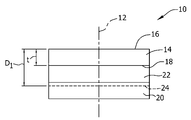
도 1a는 소자층(14), 핸들층(20) 및 중간층(22)을 포함하는 도너 구조물(10)의 횡단면도이다. 핸들층(20) 내의 점선(24)은 핸들층 내에 존재하는 손상층(24)을 나타낸다.
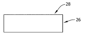
도 1b는 도 1a의 도너 구조물과 접합하기 전의 제2 구조물(26)의 횡단면도이다.
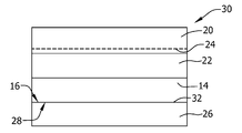
도 2는 도너 구조물의 소자층(14)의 표면(도 1a에 도시됨)과 제2 구조물(26)의 표면(도 1b에 도시됨)의 접촉에 의해 형성된 접합 구조물(30)의 횡단면도이다.
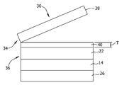
도 3은 핸들층(20) 내의 손상층(24)을 따라 접합 구조물(30)을 분리하여 소자층(14), 중간층(22) 및 그 위에 임의로 존재할 수 있는 핸들층(20)의 잔여 부분(40)을 제2 구조물(26)에 전이시키는 것을 도시하는 횡단면도이다.
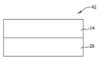
도 4는 본 발명의 다층 결정질 구조물(42)의 횡단면도이다.
상응하는 도면부호는 도면 전체에 걸쳐 상응하는 부분을 나타낸다.1A is a cross-sectional view of
FIG. 1B is a cross-sectional view of the
FIG. 2 is a cross-sectional view of the
3 separates the
4 is a cross-sectional view of the multilayer
Corresponding reference characters indicate corresponding parts throughout the drawings.
본 발명에 따라, 다층 결정질 구조물의 개선된 제조 공정이 발견되었다. 더 구체적으로는, 층 전이 및 화학적 에칭 기술의 사용이 다층 결정질 구조물을 보다 효율적으로 제조하는 개선된 방법을 제공한다는 것이 발견되었다. 본 발명에 따라, 도너 구조물은 일반적으로 소자층, 핸들 웨이퍼, 및 이들 사이에 배치된 중간층을 적어도 포함하는 임의의 구조물일 수 있다. 유리하게는, 도너 구조물의 핸들 웨이퍼는 여러 번 재활용될 수 있다. 본원에서 예시를 목적으로, 도너 구조물은 SOI(silicon-on-insulator) 구조물이다.In accordance with the present invention, an improved manufacturing process for multilayer crystalline structures has been found. More specifically, it has been found that the use of layer transfer and chemical etching techniques provide an improved method of making multilayer crystalline structures more efficiently. In accordance with the present invention, the donor structure may generally be any structure including at least a device layer, a handle wafer, and an intermediate layer disposed therebetween. Advantageously, the handle wafer of the donor structure can be recycled many times. For purposes of illustration herein, the donor structure is a silicon-on-insulator (SOI) structure.
본 발명의 예시적인 실시양태에서 도너 구조물을 위해 사용되는 SOI 구조물은 공지된 공정에 의해 형성될 수 있다는 것을 유념해야 한다. 이러한 공정은, 예를 들어, 산소 이온 주입에 의한 SOI 형성(Simox), 반도체 웨이퍼를 산화된 핸들에 접합하고 반도체 웨이퍼의 일부를 연삭/에칭하는 것(BESOI), 또는 전문이 모든 목적을 위해 본원에 참고로 인용된 미국특허출원공개 제2007/0041566호 및 제2007/0117350호에 기술된 접합 및 층 전이 기술을 포함한다. 바람직하게는, 본 발명의 공정은 도너 구조물을 제조하는 데에 웨이퍼 접합 및 층 전이 기술을 사용한다. 따라서 본 발명은 이러한 기술에 관련하여 하기에서 보다 상세하게 설명될 것이다. 그러나, 이는 예시를 위한 것이지 제한 개념으로 여겨져서는 안 된다는 것을 이해해야 한다. 또한, 본 발명의 실시에서, 이러한 기술을 적합하게는 해당 분야에 잘 공지된 다양한 장치 및 공정 조건을 사용하여 수행할 수 있고, 몇몇 경우에는, 본 발명의 범주에서 벗어나지 않게 이러한 기술을 생략하거나 기타 기술 및 조건과 조합할 수 있다는 것을 이해해야 한다.It should be noted that the SOI structure used for the donor structure in an exemplary embodiment of the present invention may be formed by known processes. Such a process may be, for example, SOI formation by oxygen ion implantation (Simox), bonding a semiconductor wafer to an oxidized handle and grinding / etching a portion of the semiconductor wafer (BESOI), or a full text for all purposes herein. Bonding and layer transfer techniques described in US 2007/0041566 and 2007/0117350, which are incorporated herein by reference. Preferably, the process of the present invention uses wafer bonding and layer transfer techniques to fabricate donor structures. The invention will therefore be described in more detail below in connection with this technique. However, it should be understood that this is for illustration only and should not be considered a limiting concept. In addition, in the practice of the present invention, such techniques may suitably be carried out using various apparatus and process conditions well known in the art, and in some cases, such techniques may be omitted or otherwise without departing from the scope of the present invention. It is to be understood that the combination with the techniques and conditions is possible.
1. 다층 결정질 구조물의 형성1. Formation of multilayer crystalline structures
이온을, 소자층, 핸들층 및 중간층을 포함하는 도너 구조물 내에 주입하고, 도너 구조물을 제2 구조물에 접합하여 접합 구조물을 형성하고, 핸들층의 일부 또는 전부 및 임의로 중간층의 일부를, 여전히 제2 구조물에 접합된 소자층으로부터 쪼개고, 임의로 잔여 핸들층 및/또는 중간층의 전부 또는 일부를 소자층으로부터 에칭하여 소자층을 노출시킴으로써, 본 발명의 다층 결정질 구조물을 제조할 수 있다. 한 실시양태에서, 제1 구조물(본원에서는 "도너 구조물"이라고 지칭됨)은 SOI 구조물이고, 제2 구조물은 사파이어 웨이퍼이다.Ions are implanted into a donor structure comprising a device layer, a handle layer and an intermediate layer, the donor structure is bonded to a second structure to form a junction structure, and some or all of the handle layer and optionally a portion of the intermediate layer are still second The multilayer crystalline structure of the present invention can be prepared by cleaving from the device layer bonded to the structure, and optionally etching all or part of the remaining handle layer and / or intermediate layer from the device layer to expose the device layer. In one embodiment, the first structure (herein referred to as the "donor structure") is an SOI structure and the second structure is a sapphire wafer.
도너 구조물은 최종 다층 결정질 구조물에 소자층을 제공한다. 기타 기판은 이후부터는 "제2 구조물"이라고 지칭될 것이다. 제2 구조물은 사파이어, 석영 결정, 탄화규소, 규소 또는 유리로 이루어질 수 있다. 한 대안적 실시양태에서, 도너 구조물을 제2 구조물에 접합하기 전에, 상당한 양의 접합층을 도너 구조물 또는 제2 구조물 중 하나 이상 상에 배치한다.The donor structure provides the device layer to the final multilayer crystalline structure. Other substrates will hereinafter be referred to as "second structures". The second structure may be made of sapphire, quartz crystal, silicon carbide, silicon or glass. In an alternative embodiment, a significant amount of bonding layer is disposed on at least one of the donor structure or the second structure prior to bonding the donor structure to the second structure.
A. 도너 구조물A. Donor Structure
이제 도 1a를 보자면, 도너 구조물(10)은 중심축(12) 및 소자층(14)을 포함하고, 여기서 소자층(14)은 주입 표면(16) 및 소자 표면(18)을 포함한다. 주입 표면(16) 및 소자 표면(18)은 중심축(12)에 대해 대체로 수직이다. 평균 두께 t는 소자층(14)의 주입 표면(16)으로부터 소자 표면(18)까지 축방향으로 연장된다. 도너 구조물(10)은 핸들층(20) 및 중간층(22)을 추가로 포함하고, 중간층(22)은 소자 표면(18)과 핸들층(20) 사이에서 도너 구조물(10)의 중심축(12)을 따라 배치된다.Referring now to FIG. 1A, the
소자층은 마이크로 전자 소자 또는 광기전력 소자의 제조에서의 사용에 적합한 임의의 물질을 포함한다. 소자층은 전형적으로, 규소, 탄화규소, 사파이어, 게르마늄, 실리콘 게르마늄, 질화갈륨, 질화알루미늄 또는 이것들의 임의의 조합으로 이루어진 군으로부터 선택된 물질을 포함한다. 한 바람직한 실시양태에서, 소자층은 규소를 포함한다.The device layer includes any material suitable for use in the manufacture of microelectronic devices or photovoltaic devices. The device layer typically comprises a material selected from the group consisting of silicon, silicon carbide, sapphire, germanium, silicon germanium, gallium nitride, aluminum nitride or any combination thereof. In one preferred embodiment, the device layer comprises silicon.
일반적으로, 소자층은, 마이크로 전자 소자 또는 광기전력 소자의 제조에서의 사용에 적합한 평균 두께 t를 갖지만, 소자층은 본 발명의 범주에서 벗어나지 않게 전형적으로 사용되는 것보다 더 큰 두께를 가질 수 있다. 일반적으로, 소자층은 약 20 ㎚ 이상, 전형적으로 약 90 ㎚ 이상의 평균 두께 t를 갖고, 약 20 ㎚ 내지 약 500 ㎚의 두께 t를 가질 수 있다.In general, the device layer has an average thickness t suitable for use in the manufacture of microelectronic devices or photovoltaic devices, but the device layer may have a larger thickness than typically used without departing from the scope of the present invention. . In general, the device layer has an average thickness t of at least about 20 nm, typically at least about 90 nm, and may have a thickness t of about 20 nm to about 500 nm.
중간층은 소자층 및 핸들층 둘 다에 부착될 수 있는, 이온 주입에 의해 침투될 수 있는 임의의 물질일 수 있다. 전형적으로, 중간층은 유전층이고, 이산화규소 및 질화규소로 이루어진 군으로부터 선택된 물질을 포함한다. 일반적으로, 중간층은 약 10 ㎚ 이상, 전형적으로 약 500 ㎚ 이상의 평균 두께를 갖는다.The intermediate layer can be any material that can be penetrated by ion implantation, which can be attached to both the device layer and the handle layer. Typically, the intermediate layer is a dielectric layer and comprises a material selected from the group consisting of silicon dioxide and silicon nitride. Generally, the interlayer has an average thickness of at least about 10 nm, typically at least about 500 nm.
핸들층은, 그 위에 중간층이 침착(deposit)될 수 있는 임의의 물질일 수 있다. 본 발명의 몇몇 실시양태에서, 이온을 핸들층에 주입한다. 이러한 실시양태에서, 핸들층은 이온 주입에 적합한 물질을 포함하며, 해당 분야에 공지된 이온 주입 및 층분리 기술에 의해 쪼개질 수 있다. 전형적으로, 핸들층은 규소, 탄화규소, 사파이어, 게르마늄, 실리콘 게르마늄, 질화갈륨, 질화알루미늄, 갈륨 비소, 인듐 갈륨 비소 또는 이것들의 임의의 조합으로 이루어진 군으로부터 선택된 물질을 포함한다.The handle layer can be any material from which an intermediate layer can be deposited. In some embodiments of the invention, ions are implanted into the handle layer. In such embodiments, the handle layer comprises a material suitable for ion implantation and can be cleaved by ion implantation and layer separation techniques known in the art. Typically, the handle layer comprises a material selected from the group consisting of silicon, silicon carbide, sapphire, germanium, silicon germanium, gallium nitride, aluminum nitride, gallium arsenide, indium gallium arsenide, or any combination thereof.
일반적으로, 핸들층은, 본 발명의 범주에서 벗어나지 않게 소자층 및 중간층의 적어도 일부 및 임의로 핸들층의 일부의 층분리를 허용하기에 충분한 구조적 일체성을 제공할 수 있는 임의의 두께를 가질 수 있다. 일반적으로, 핸들층은 약 100 마이크로미터 이상, 전형적으로는 약 200 마이크로미터 이상의 평균 두께를 가질 수 있고, 약 100 내지 약 900 마이크로미터, 심지어는 약 500 내지 약 800 마이크로미터의 두께를 가질 수 있다.In general, the handle layer can have any thickness that can provide sufficient structural integrity to allow delamination of at least a portion of the device layer and the intermediate layer and optionally a portion of the handle layer without departing from the scope of the present invention. . In general, the handle layer may have an average thickness of at least about 100 micrometers, typically at least about 200 micrometers, and may have a thickness of about 100 to about 900 micrometers, even about 500 to about 800 micrometers. .
몇몇 실시양태에서, 도너 구조물(10)은, 이온을 도너 구조물(10) 내에 주입하기 전 또는 후 및/또는 도너 구조물(10)을 제2 구조물(26)에 접합하기 전에 주입 표면(16) 상에 형성된 접합층, 예컨대 산화물층, 침착된 산화물, TEOS, CVD 질화물 또는 유기 접착제를 추가로 포함할 수 있다. 그 대신에 또는 추가로, 접합층을, 접합 전에, 제2 구조물 상에 형성할 수 있다. 접합층을 적용하면, 도너 구조물(10)을 제2 구조물(26)에 직접 접합하는 동안에 일어날 수 있는 계면 틈새의 형성을 방지하도록 도너 구조물(10)과 제2 구조물(26) 사이의 접합 계면이 제공된다. 필요한 것은 아니지만, 접합층은 존재한다면, 10 ㎚ 이상의 평균 두께를 가질 수 있고, 약 1 마이크로미터 이상, 약 3 마이크로미터 이상 또는 그 초과의 평균 두께를 가질 수 있다.In some embodiments, the
해당 분야에 일반적으로 공지된 임의의 기술을 사용하여 도너 구조물을 형성할 수 있다는 것을 유념해야 한다. 예를 들어, 도너 구조물을 층 전이 공정, 배면 에칭 공정 또는 SIMOX 공정을 사용하여 형성할 수 있다.It should be noted that the donor structure can be formed using any technique generally known in the art. For example, the donor structure can be formed using a layer transfer process, a back etching process or a SIMOX process.
또한, 상기에서 설명된 범위 및 최소 두께 값은, 이러한 두께가 상기에서 언급된 임의의 공정을 통해 소자층을 제2 구조물에 전이시키는 데 충분하다면, 한정적으로 본 발명에만 중요한 것은 아니라는 것을 유념해야 한다.It should also be noted that the ranges and minimum thickness values described above are not critical to the present invention, as long as such thicknesses are sufficient to transfer the device layer to the second structure through any of the processes mentioned above. .
다시 도 1a를 보자면, 이온, 예컨대 수소 및/또는 헬륨 이온을 실질적으로 균일한 깊이로 주입 표면(16)을 통해 주입한다. 예시적인 실시양태에서, 이온을 주입 표면(16)을 통해 핸들층(20) 내에 주입 깊이 D1까지 주입하는데, 여기서 D1은 소자층과 중간층의 합산된 두께보다 더 크다. 그러나, 또 다른 실시양태에서는, 이온을, 이온이 핸들층에 도달하지 않도록 주입 표면(16)을 통해 중간층(22) 내에 주입할 수 있다. 이온 주입을 수행하기 전에 접합층을 주입 표면 상에 침착시키는 실시양태에서는, 주입 깊이 D1은 접합층의 추가된 두께 때문에 증가할 수 있다는 것을 유념해야 한다. 이온 주입은 이온이 주입된 층 내에 손상층(24)을 한정한다. 예시적인 실시양태에서, 도 1a에 도시된 바와 같이, 이온 주입은 핸들층(20) 내에 손상층(24)을 한정한다.Referring again to FIG. 1A, ions, such as hydrogen and / or helium ions, are implanted through the
일반적으로, 이온을, 후속 접합 및 쪼갬 공정에서 소자층(14)의 만족스러운 전이를 보장하기에 충분한 평균 깊이까지 주입한다. 바람직하게는, 소자층과 함께 전이되는 핸들층(20) 및/또는 중간층의 양을 감소시키도록, 주입 깊이를 최소화한다. 일반적으로, 이온을, 소자층 및 중간층의 두께에 따라서는, 주입 표면 아래 약 200 옹스트롬 이상 또는 심지어는 약 1 마이크로미터 이상의 깊이까지 주입한다. 몇몇 실시양태에서, 이온을 약 20 ㎚ 이상, 전형적으로 약 90 ㎚ 이상, 약 250 ㎚ 이상 또는 심지어는 약 500 ㎚ 이상의 깊이까지 주입할 수 있다. 그러나, 보다 깊은 주입 깊이라도 소자층을 노출시키기 위한 쪼갬 후에 제거되어야 할 중간층 및/또는 핸들층의 양을 단지 증가시킬 뿐이므로, 본 발명의 범주에서 벗어나지 않게 보다 깊은 주입 깊이를 사용할 수 있다는 것을 유념해야 한다. 따라서, 약 200 옹스트롬 내지 약 1 마이크로미터 또는 심지어는 약 20 ㎚ 내지 약 500 ㎚의 깊이까지 이온을 주입하는 것이 바람직할 수 있다.Generally, ions are implanted to an average depth sufficient to ensure satisfactory transition of the
이온 주입을 해당 분야에 공지된 수단을 사용하여 달성할 수 있다. 예를 들어, 전문이 본원에 참고로 포함된 미국특허 제6,790,747호의 공정에 따르는 방식으로 이온 주입을 달성할 수 있다. 몇몇 실시양태에서는, 예를 들어 약 10 keV 이상, 약 20 keV 이상, 약 80 keV 이상, 또는 약 120 keV 이상의 에너지를 사용하여 수소를 약 1 × 10¹⁶ 이온/㎠ 이상, 약 2 × 10¹⁶ 이온/㎠ 이상, 약 1 × 10¹⁷ 이온/㎠ 이상, 또는 심지어는 약 2 × 10¹⁷ 이온/㎠ 이상의 주입량(dosage)으로 주입할 수 있다. 전형적으로, 주입되는 수소의 농도는 약 2 × 10¹⁶ 이온/㎠ 내지 약 6 × 10¹⁶ 이온/㎠일 수 있다. 수소를 본 발명의 범주에서 벗어나지 않게 H2 + 또는 또 다르게는 H+로서 주입할 수 있다는 것을 유념해야 한다.Ion implantation can be accomplished using means known in the art. For example, ion implantation can be accomplished in a manner according to the process of US Pat. No. 6,790,747, which is incorporated herein by reference in its entirety. In some embodiments, e.g., at least about 10 keV, at least about 20 keV, at least about 80 keV, or hydrogen with at least about 120 keV energy of about 1 × 10 16 ions / ㎠, at least about 2 × 10 16 ions Or at an injection dose of at least about 1 × 10 17 ions / cm 2 or even at least about 2 × 10 17 ions / cm 2. Typically, the concentration of hydrogen injected may be about 2 × 10 16 ions / cm 2 to about 6 × 10 16 ions / cm 2. It should be noted that hydrogen can be injected as H 2 + or alternatively H + without departing from the scope of the invention.
또 다른 실시양태에서, 예를 들어 약 10 keV 이상, 약 20 keV 이상, 약 30 keV 이상, 약 50 keV 이상, 약 80 keV 이상, 또는 심지어는 약 120 keV 이상의 에너지를 사용하여 헬륨을 약 5 × 10¹⁵ 이온/㎠ 이상, 약 1 × 10¹⁶ 이온/㎠ 이상, 약 5 × 10¹⁶ 이온/㎠ 이상, 또는 심지어는 약 1 × 10¹⁷ 이온/㎠ 이상의 주입량으로 주입할 수 있다. 전형적으로, 주입되는 헬륨의 농도는 약 1 × 10¹⁶ 이온/㎠ 내지 약 3 × 10¹⁶ 이온/㎠일 수 있다.In another embodiment, for example, at least about 10 keV, at least about 20 keV, at least about 30 keV, at least about 50 keV, at least about 80 keV, or even at least about 120 keV, using about 5 × 10 15 ions / cm 2 or more, about 1 × 10 16 ions / cm 2 or more, about 5 × 10 16 ions / cm 2 or more, or even about 1 × 10 17 ions / cm 2 or more. Typically, the concentration of helium implanted may be between about 1 × 10 16 ions / cm 2 and about 3 × 10 16 ions / cm 2.
기타 실시양태에서는, 수소 및 헬륨 이온 둘 다를 주입한다. 수소 및 헬륨 둘 다를 조합으로 주입하는 것을 동시에 수행하거나, 헬륨을 주입하기 전에 수소를 주입하거나 또 다르게는 수소를 주입하기 전에 헬륨을 주입함으로써, 순차적으로 수행할 수 있다는 것을 유념해야 한다. 바람직하게는, 수소 및 헬륨을 순차적으로 주입하는데, 먼저 헬륨을, 약 10 keV 이상, 약 20 keV 이상, 약 30 keV 이상, 약 50 keV 이상, 약 80 keV 이상, 또는 심지어는 약 120 keV 이상을 사용하여 약 5 × 10¹⁵ 이온/㎠ 이상, 약 1 × 10¹⁶ 이온/㎠ 이상, 약 5 × 10¹⁶ 이온/㎠ 이상, 또는 심지어는 약 1 × 10¹⁷ 이온/㎠ 이상의 주입량으로 주입하고, 이어서 수소를, 약 10 keV 이상, 약 20 keV 이상, 약 30 keV 이상, 약 50 keV 이상, 약 80 keV 이상, 또는 심지어는 약 120 keV 이상을 사용하여 약 5 × 10¹⁵ 이온/㎠ 이상, 약 1 × 10¹⁶ 이온/㎠ 이상, 약 5 × 10¹⁶ 이온/㎠ 이상, 또는 심지어는 약 1 × 10¹⁷ 이온/㎠ 이상의 주입량으로, 헬륨과 실질적으로 동일한 깊이로 주입한다. 한 실시양태에서, 예를 들어 약 1 × 10¹⁶ He+ 이온/㎠을 약 36 keV를 사용하여 도너 구조물 내에 주입하고, 이어서 도너 구조물 내에 약 0.5 × 10¹⁶ H2 + 이온/㎠을 약 48 keV에서 주입하거나 또 다르게는 약 1 × 10¹⁶ H+ 이온/㎠을 약 24 keV에서 주입한다. 이온을 도너 구조물 내에 주입하는 것을 수행하는 데 필요한 에너지의 구체적인 양은 선택된 이온(들)의 유형 및 형태, 이온이 주입되면서 통과하는 물질 및 이온이 주입되는 물질의 결정학적 구조 및 원하는 주입 깊이에 따라 달라진다. 이온 주입을 이러한 이온 주입에 적합한 임의의 온도에서 수행할 수 있다는 것을 유념해야 한다. 그러나, 전형적으로, 이온 주입을 실온에서 수행할 수 있다. 또한, 이와 관련해서, 언급된 이온 주입 온도는 전역적 온도라는 것과, 이온 주입의 본질로 인해 이온 빔의 실제 부위에서 국지적 온도 스파이크가 일어날 수 있다는 것을 유념해야 한다.In other embodiments, both hydrogen and helium ions are implanted. It should be noted that the implantation of both hydrogen and helium may be performed sequentially, either by simultaneously injecting hydrogen before helium, or alternatively by injecting helium before hydrogen. Preferably, hydrogen and helium are injected sequentially, with helium first being at least about 10 keV, at least about 20 keV, at least about 30 keV, at least about 50 keV, at least about 80 keV, or even at least about 120 keV. Using at least about 5 × 10 15 ions / cm 2, at least about 1 × 10 16 ions / cm 2, at least about 5 × 10 16 ions / cm 2, or even at least about 1 × 10 17 ions / cm 2, Hydrogen is used at least about 5 × 10 15 ions / cm 2, at least about 10 keV, at least about 20 keV, at least about 30 keV, at least about 50 keV, at least about 80 keV, or even at least about 120 keV. At an implantation dose of at least 10 16 ions / cm 2, at least about 5 × 10 16 ions / cm 2, or even at least about 1 × 10 17 ions / cm 2, implanted at a depth substantially the same as helium. In one embodiment, for example, about 1 × 10 16 He + ions / cm 2 are injected into the donor structure using about 36 keV, and then about 0.5 × 10 16 H 2 + ions / cm 2 is about 48 keV into the donor structure. Or alternatively about 1 × 10 16 H + ions / cm 2 at about 24 keV. The specific amount of energy required to perform implantation of ions into the donor structure depends on the type and form of the selected ion (s), the crystallographic structure of the material through which the ion is implanted and the material into which the ion is implanted, and the desired implantation depth. . It should be noted that ion implantation can be performed at any temperature suitable for such ion implantation. Typically, however, ion implantation can be performed at room temperature. Also in this regard, it should be noted that the ion implantation temperature mentioned is a global temperature and that local temperature spikes may occur at the actual site of the ion beam due to the nature of the ion implantation.
이온 주입을 수행한 후에, 도너 구조물(10)을 열처리하여 손상층(24)에서 벽개면을 형성하기 시작할 수 있다. 예를 들어, 도너 구조물을 약 150 ℃ 내지 약 375 ℃의 온도에서 약 1 시간 내지 약 100 시간 동안 열처리할 수 있다. 또 다른 실시양태에서는, 하기에서 기술되는 바와 같이, 도너 구조물(10)과 제2 구조물(26) 사이의 접합을 강화함과 동시에 손상층(24)에서의 벽개면의 형성을 시작하기 위해서, 이러한 열처리를, 도너 구조물(10)을 제2 구조물(26)에 접합한 후에 수행되는 열처리와 조합할 수 있다.After ion implantation is performed, the
B. 핸들 웨이퍼 구조물B. Handle Wafer Structure
이제 도 1b를 보자면, 제2 구조물(26)은 접합 표면(28)을 갖는 단일 웨이퍼 또는 다층 웨이퍼를 포함한다. 예시적인 실시양태에서는, 도 1b에 도시된 바와 같이, 제2 구조물(26)은 단일 웨이퍼이다. 제2 구조물(26)은 사파이어, 석영 결정, 유리, 탄화규소, 규소, 질화갈륨, 질화알루미늄, 갈륨 알루미늄 질화물, 또는 이것들의 임의의 조합으로 이루어진 군으로부터 선택된 물질로 이루어질 수 있다. 한 바람직한 실시양태에서, 제2 구조물(26)은 사파이어 웨이퍼를 포함한다.Referring now to FIG. 1B, the
C. 웨이퍼 접합 및 소자층의 전이C. Wafer Bonding and Transition of Device Layers
일단 도너 구조물(10) 및 제2 구조물(26)을 제조 또는 선택하고 나면, 최종 다층 결정질 구조물의 형성은 도너 구조물(10)의 소자층(14)을 제2 구조물(26) 상에 전이시키는 것을 포함한다. 일반적으로 말하자면, 소자층(14)의 주입 표면(16)과 제2 구조물(26)의 접합 표면(28) 사이에 접합 계면(32)을 갖는 단일 접합 구조물(30)을 형성하기 위해서 소자층(14)의 주입 표면(16)과 제2 구조물(26)의 접합 표면(28)을 접촉시키고, 이어서 접합 구조물을 손상층(24)을 따라 형성된 벽개면을 따라 쪼갬 또는 분리함으로써, 이러한 전이를 달성한다.Once the
접합 전에, 주입 표면(16) 및/또는 접합 표면(28)을 임의로, 해당 분야에 공지된 기술을 사용하여, 세정, 단시간 에칭 및/또는 평탄화하여 이러한 표면을 접합에 적합하도록 만들 수 있다. 특정 이론에 의해 얽매이는 일 없이, 일반적으로 접합 전의 두 표면의 품질은 그 결과의 접합 계면의 품질 또는 강도에 직접적인 영향을 미칠 것이라고 생각된다.Prior to bonding, the
주입 표면(16) 및/또는 접합 표면(28)을 추가로 컨디셔닝하는 대신에 또는 추가로, 도너 구조물을 제2 구조물에 접합하기 전에, 접합층을 주입 표면 및/또는 접합 표면 상에 형성할 수 있다. 접합층을 도너 구조물 상에 형성할 때, 이러한 형성을 이온 주입 단계 전 또는 후에 수행할 수 있다는 것을 유념해야 한다. 접합층은 도너 구조물을 제2 구조물에 접합하는 데 적합한 임의의 물질, 예를 들어 산화물층, 예컨대 이산화규소, 질화규소, 침착된 산화물, 예컨대 TEOS 및 접합 접착제를 포함할 수 있다. 특정 이론에 의해 얽매이는 일 없이, 접합층을 포함시킴으로써, 도너 구조물(10)과 제2 구조물(26)을 직접 접합하는 동안에 일어날 수 있는 계면 틈새의 형성을 방지하도록 도너 구조물(10)과 제2 구조물(26) 사이에 접합 계면이 제공된다. 열적 산화물 성장 온도는 적어도 약 800 ℃ 내지 약 1100 ℃의 범위일 수 있고, 접합층의 두께는 전형적으로 약 10 ㎚ 내지 약 200 ㎚의 범위이다. 접합층이 성장할 때 주변의 대기는 전형적으로, 건식 산화의 경우에는 산소, 질소, 아르곤 및/또는 이것들의 혼합물 및 습식 산화의 경우에는 수증기를 포함한다. CVD 증착된 산화물을 전형적으로 저온(즉 약 400 ℃ 내지 약 600 ℃)에서 증착시킨다. 추가로, 몇몇 접합 접착제를 실온 또는 그보다 약간 더 높은 온도에서 1 마이크로미터 이상의 두께로 도포할 수 있고, 이어서 약 200 ℃의 온도에서 하소 또는 경화시킬 수 있다.Instead of or in addition to further conditioning the
표면 조도는 표면의 품질을 정량적으로 측정하는 하나의 방식이며 보다 낮은 표면 조도 값은 보다 높은 품질의 표면에 상응한다. 따라서, 소자층(14)의 주입 표면(16) 및/또는 제2 구조물(26)의 접합 표면(28)을 표면 조도를 감소시키는 가공에 적용시킬 수 있다. 예를 들어, 한 실시양태에서, 표면 조도는 약 5 옹스트롬 미만이다. 이러한 감소된 RMS 값을, 접합 전에 세정 및/또는 평탄화를 통해 달성할 수 있다. 세정을 습식 화학적 세정 공정, 예컨대 친수성 표면 제조 공정에 따라 수행할 수 있다. 하나의 통상적인 친수성 표면 제조 공정은 RCA SC1 세정 공정이고, 이러한 공정에서는 표면을 예를 들어 1:4:20의 비의 수산화암모늄, 과산화수소 및 물을 포함하는 용액과 약 60 ℃에서 약 10 분 동안 접촉시키고, 이어서 탈이온수로써 헹구고 회전건조시킨다. 평탄화를 화학-기계적 연마(CMP) 기술을 사용하여 수행할 수 있다. 또한, 표면들 중 하나 또는 둘 다를, 습식 세정 공정 전, 후 또는 대신에, 플라스마 활성화에 적용시켜 그 결과의 접합 강도를 증가시킬 수 있다. 플라스마 환경은 예를 들어 산소, 암모니아, 아르곤, 질소, 디보란 또는 포스핀을 포함할 수 있다. 한 바람직한 실시양태에서, 플라스마 활성화 환경은 질소, 산소 및 이것들의 조합으로 이루어진 군으로부터 선택된다.Surface roughness is one way of quantitatively measuring the quality of a surface and lower surface roughness values correspond to higher quality surfaces. Thus, the
이제 도 2를 보자면, 소자층(14)의 주입 표면(16)과 제2 구조물(26)의 접합 표면(28)을 접촉시켜 접합 계면(32)를 형성함으로써, 도너 구조물(10)을 제2 구조물(26)에 접합한다. 일반적으로 말하자면, 본질적으로 해당 분야에 공지된 임의의 기술을 사용하여 웨이퍼 접합을 달성할 수 있는데, 단 접합 계면의 형성을 달성하는 데 사용되는 에너지는, 후속 가공 동안에, 예컨대 쪼갬 또는 분리에 의한 층 전이 동안에 접합 계면의 일체성이 유지되는 것을 보장하기에 충분해야 한다. 그러나, 전형적으로, 소자층의 표면과 제2 구조물을 실온에서 접촉시킨 후, 약 500 mJ/㎡ 초과, 약 750 mJ/㎡, 약 1000 mJ/㎡ 또는 그 초과의 접합 강도를 갖는 접합 계면을 형성하기에 충분한 시간 동안 저온 어닐링시킴으로써, 웨이퍼 접합을 달성한다. 이러한 접합 강도 값을 달성하기 위해서는, 전형적으로 가열을 적어도 약 200 ℃, 300 ℃, 400 ℃ 또는 심지어는 500 ℃의 온도에서, 적어도 약 5 분, 30 분, 60 분, 또는 심지어는 300 분의 시간 동안 수행한다. 상기에서 기술된 바와 같이, 한 실시양태에서, 이러한 저온 열적 어닐링을, 상기에서 기술된, 접합 전 도너 구조물(10)의 열처리에 추가하여 또는 대신에 수행할 수 있다. 도너 구조물(10)을 접합 전에 열적으로 어닐링하지 않는 실시양태에서는, 접합 구조물(30)의 저온 열적 어닐링은 접합 계면의 강화뿐만 아니라 손상층(24)을 따라 위치하는 벽개면의 형성을 용이하게 한다.Referring now to FIG. 2, the
이제 도 3을 보자면, 접합 표면(32)을 형성한 후에, 그 결과의 접합 구조물(30)을, 핸들층(20) 내의 손상층(24)을 따라 균열을 유도하기에 충분한 조건에 적용시킨다. 일반적으로 말하자면, 이러한 균열을 해당 분야에 공지된 기술을 사용하여, 예컨대 기계적 또는 열적 쪼갬을 사용하여 달성할 수 있다. 그러나, 전형적으로, 균열을 유도하는 시간 동안 승온에서 접합 구조물을 어닐링함으로써 균열을 달성한다. 예를 들어, 어닐링 온도는 적어도 약 200 ℃, 적어도 약 250 ℃ 또는 그 초과일 수 있다. 몇몇 실시양태에서, 어닐링을 심지어는 적어도 약 350 ℃, 450 ℃, 550 ℃, 650 ℃, 또는 심지어는 750 ℃의 온도, 전형적으로는 약 200 ℃ 내지 약 750 ℃ 및 보다 전형적으로는 약 200 ℃ 내지 약 400 ℃의 온도에서 수행할 수 있다. 그러나, 포함된 다양한 물질(예를 들어, 규소 및 사파이어)의 상이한 열팽창계수 때문에, 도너 물질과 핸들 사이의 열적 불일치로 인해 상기에서 언급된 어닐링을 보다 낮은 온도에서 수행하는 것이 종종 바람직하다는 것을 유념해야 한다. 따라서, 어닐링을 바람직하게는 약 200 ℃ 내지 약 300 ℃의 어닐링 온도를 사용하여 수행할 수 있다. 어닐링을 적어도 약 5 분, 30 분, 60 분 또는 심지어는 300 분의 시간 동안 수행한다. 보다 높은 어닐링 온도는 보다 짧은 어닐링 시간을 필요로 하며, 또한 반대도 그러하다. 어닐링 단계를 주위 또는 불활성 대기, 예를 들어 아르곤 또는 질소 중에서 수행할 수 있다.Referring now to FIG. 3, after forming the
한 바람직한 실시양태에서, 분리(즉 핸들층(20) 내의 손상층(24)를 따라 구조물을 균열시킴)는 단독으로 또는 어닐링 공정에 추가하여 기계적 힘을 가하는 것을 포함한다. 이러한 기계적 힘을 가하는 실제 수단은 본 발명에서는 중요하지 않은데, 즉 소자층에 상당한 손상이 가해지는 것이 회피되는 한, 반도체 구조물에서 분리를 유도하는 기계적 힘을 가하는 임의의 공지된 방법을 사용할 수 있다.In one preferred embodiment, separation (i.e., cracking the structure along the
다시 도 3을 보자면, 분리 시 두 구조물(34 및 36)이 형성된다. 접합 구조물(30)의 분리가 핸들층(20) 내의 손상층(24)을 따라 발생하는 경우에, 벽개면은 접합 계면(32)과 일치하지 않고, 오히려 핸들층(20) 내에 존재하며, 핸들층의 일부는 두 구조물의 일부(즉, 핸들층의 일부는 중간층(22) 및 소자층(14)과 함께 전이됨)이다. 예시적인 실시양태에서, 구조물(34)는 핸들층(20)의 일부(38)를 포함한다. 구조물(36)은 제2 구조물(26), 소자층(14), 중간층(22), 및 그의 표면 상의 핸들층(20)의 잔여 부분(40)을 포함한다. 이온을, 손상층을 완전히 중간층 내에 형성하는 깊이까지 주입하는 대안적 실시양태에서는, 구조물(34)은 전체 핸들층 및 임의로 중간층의 일부를 포함하고, 구조물(36)은 제2 구조물(26), 소자층(14), 및 중간층(22)의 전부 또는 일부를 포함한다.Referring again to FIG. 3, two
핸들층(20)의 잔여 부분(40)이 존재하는 경우, 이것은 이온이 핸들층(20) 내에 주입된 깊이와 대략 동일한 두께(T)를 갖는다. 따라서, 이러한 두께(T)는 전형적으로 약 10 ㎚ 초과이다. 예를 들어, 몇몇 경우에서, 잔여 층은 임의로 적어도 약 20 ㎚, 50 ㎚, 75 ㎚, 100 ㎚, 200 ㎚ 또는 그 초과의 두께를 가질 수 있다. 바람직하게는 두께(T)는 분리 시 소자층(14)의 손상을 회피하기에 충분하고, 예를 들어, 한 바람직한 실시양태에서, 잔여 부분은 약 20 ㎚ 내지 약 200 ㎚의 두께를 갖는다.If the remaining
2. 층 전이 후의 다층 결정질 구조의 마감 처리2. Finishing of Multi-Layered Crystalline Structures After Layer Transition
A. 잔여 핸들층의 제거A. Removal of Residual Handle Layers
본 발명에 따라 그리고 도 3 및 4를 보자면, 소자층(14), 중간층(22)의 적어도 일부 및 임의로 핸들층(20)의 잔여 부분(40)을 제2 구조물(26)에 전이시켜 접합 구조물(30)을 형성한 후에, 접합 구조물(30)을 추가의 가공에 적용시켜, 소자 제작에 바람직한 특성을 갖는 다층 결정질 구조물을 제조한다. 예를 들어, 핸들층(20)의 잔여 부분(40)이 존재하는 경우, 이러한 잔여 부분뿐만 아니라 중간층(22)을 제거하기 위해서 접합 구조물(30)을 하나 이상의 가공 단계에 적용시킬 수 있다. 비록 해당 분야에 공지된 본질적으로 임의의 기술을 사용할 수 있지만, 잔여 부분(40) 및 중간층(22)을 바람직하게는 에칭을 통해 제거한다. 에칭 조성물을, 핸들층(20)의 잔여 부분(40)의 조성, 중간층(22)의 조성 및 에칭제의 선택도를 포함하는 다양한 인자에 따라 선택할 수 있다. 한 실시양태에서, 핸들층(20)의 전체 잔여 부분(40) 및 실질적으로 전체 중간층(22)을, NH4OH, H2O2 및 H2O를 포함하는 에칭제를 사용하는 습식 에칭 공정을 통해 제거한다. 이러한 에칭제는 일반적으로 해당 분야의 숙련자에게 공지되어 있고 통상적으로 "SC1" 용액으로서 지칭된다. 이러한 에칭 공정을 전형적으로 약 50 ℃ 내지 약 80 ℃의 온도에서 수행하며, 이러한 에칭의 시간은 제거될 층의 두께, SC1 조성물의 정확한 조성, 및 에칭이 수행되는 온도에 따라 달라진다. 또 다른 실시양태에서, KOH 용액을 사용하여 핸들층을 제거할 수 있고, HF 용액을 사용하여 중간층을 제거할 수 있다. 유리하게는, HF 용액은 소자층 표면을 거칠게 하지 않고서도 중간층을 제거할 것이다. 또 다른 실시양태에서, SC1 용액을 사용하여 핸들층을 제거하고 HF 용액을 사용하여 중간층을 제거한다.In accordance with the present invention and with reference to FIGS. 3 and 4, the junction structure is transferred by transferring the
도 4에 도시된 바와 같이, 최종 다층 결정질 구조물(42)은 제2 구조물(26) 및 소자층(14)를 포함한다. 한 바람직한 실시양태에서, 최종 다층 결정질 구조물(42)은 규소층이 접합된 사파이어층을 포함한다.As shown in FIG. 4, the final
3. 다층 결정질 구조물3. Multilayer crystalline structure
본 발명에 따라 제조된 다층 결정질 구조물은 약 300 ㎛ 내지 약 800 ㎛의 범위의 실질적으로 균일한 두께를 가질 수 있다. 바람직하게는, 이러한 또는 기타 실시양태에서, 소자층은 약 20 ㎚ 내지 약 200 ㎚의 범위의 두께를 갖고, 제2 구조물은 약 300 ㎛ 내지 약 800 ㎛의 두께를 갖는다.The multilayer crystalline structure made in accordance with the present invention may have a substantially uniform thickness in the range of about 300 μm to about 800 μm. Preferably, in this or other embodiments, the device layer has a thickness in the range of about 20 nm to about 200 nm and the second structure has a thickness of about 300 μm to about 800 μm.
본 발명에 따라 제조된 다층 결정질 구조물은 다양한 기술에서 사용될 수 있다. 예를 들어, 본 발명의 다층 결정질 구조물은 마이크로 전자 소자 및 본 발명의 다층 결정질 구조물을 포함하는 다층 마이크로 전자 소자의 제작에서의 사용에 적합하다. 적합한 마이크로 전자 소자는 트랜지스터 및 안테나 구조물을 포함하지만 이것으로만 제한되는 것은 아니다.Multilayer crystalline structures made in accordance with the present invention can be used in a variety of techniques. For example, the multilayer crystalline structure of the present invention is suitable for use in the fabrication of microelectronic devices and multilayer microelectronic devices comprising the multilayer crystalline structure of the present invention. Suitable microelectronic devices include, but are not limited to, transistors and antenna structures.
Claims (26)
상기 주입된 SOI 구조물을 제2 구조물에 접합하여 접합 구조물을 형성하는 단계;
상기 손상층을 따라 상기 SOI 구조물을 쪼개어 상기 제2 구조물, 상기 소자층 및 잔여 물질을 포함하는 다층 결정질 구조물을 형성하는 단계 - 상기 잔여 물질은 상기 중간층의 적어도 일부 및 임의로 상기 핸들층의 일부를 포함함 -; 및
상기 잔여 물질을 상기 다층 결정질 구조물로부터 제거하는 단계
를 포함하는, 다층 결정질 구조물의 제조 방법.Implanting ions selected from the group consisting of hydrogen, helium and combinations thereof into a silicon-on-insulator (SOI) structure, the SOI structure having a central axis, an implant surface and a device surface generally perpendicular to the central axis Device layer, wherein the device layer has an average thickness t extending axially from the injection surface of the device layer to the device surface, a handle layer, and a central axis of the SOI structure between the device surface and the handle layer. An intermediate layer disposed along, wherein said ions are implanted through said implant surface into said SOI structure to an implant depth D1 greater than the thickness t of said device layer, thereby being generally perpendicular to said axis and within said ion implanted SOI structure Forming a damage layer located within at least one of the intermediate layer and the handle layer;
Bonding the implanted SOI structure to a second structure to form a junction structure;
Splitting the SOI structure along the damage layer to form a multi-layered crystalline structure comprising the second structure, the device layer and a residual material, wherein the residual material comprises at least a portion of the intermediate layer and optionally a portion of the handle layer. Ham-; And
Removing the residual material from the multilayer crystalline structure
Including, a method of producing a multilayer crystalline structure.
Applications Claiming Priority (2)
| Application Number | Priority Date | Filing Date | Title |
|---|---|---|---|
| US29096109P | 2009-12-30 | 2009-12-30 | |
| US61/290,961 | 2009-12-30 |
Publications (1)
| Publication Number | Publication Date |
|---|---|
| KR20120117843A true KR20120117843A (en) | 2012-10-24 |
Family
ID=43587555
Family Applications (1)
| Application Number | Title | Priority Date | Filing Date |
|---|---|---|---|
| KR1020127019987A KR20120117843A (en) | 2009-12-30 | 2010-12-22 | Method for the preparation of a multi-layered crystalline structure |
Country Status (8)
| Country | Link |
|---|---|
| US (2) | US8367519B2 (en) |
| EP (2) | EP2733735A3 (en) |
| JP (2) | JP5591949B2 (en) |
| KR (1) | KR20120117843A (en) |
| CN (1) | CN103026460A (en) |
| SG (1) | SG181986A1 (en) |
| TW (2) | TWI430339B (en) |
| WO (1) | WO2011082079A1 (en) |
Cited By (1)
| Publication number | Priority date | Publication date | Assignee | Title |
|---|---|---|---|---|
| KR20150099847A (en) * | 2012-12-28 | 2015-09-01 | 썬에디슨 세미컨덕터 리미티드 | Method for low temperature layer transfer in the preparation of multilayer semiconductor devices |
Families Citing this family (6)
| Publication number | Priority date | Publication date | Assignee | Title |
|---|---|---|---|---|
| US8853054B2 (en) | 2012-03-06 | 2014-10-07 | Sunedison Semiconductor Limited | Method of manufacturing silicon-on-insulator wafers |
| US8796054B2 (en) * | 2012-05-31 | 2014-08-05 | Corning Incorporated | Gallium nitride to silicon direct wafer bonding |
| JP6024400B2 (en) | 2012-11-07 | 2016-11-16 | ソニー株式会社 | Semiconductor device, method for manufacturing semiconductor device, and antenna switch module |
| TWI509681B (en) * | 2013-11-15 | 2015-11-21 | All Ring Tech Co Ltd | Method and apparatus for processing on wafers |
| US9496128B1 (en) | 2015-10-15 | 2016-11-15 | International Business Machines Corporation | Controlled spalling utilizing vaporizable release layers |
| JP7160943B2 (en) | 2018-04-27 | 2022-10-25 | グローバルウェーハズ カンパニー リミテッド | Photo-assisted platelet formation to facilitate layer transfer from semiconductor donor substrates |
Family Cites Families (31)
| Publication number | Priority date | Publication date | Assignee | Title |
|---|---|---|---|---|
| US6033974A (en) | 1997-05-12 | 2000-03-07 | Silicon Genesis Corporation | Method for controlled cleaving process |
| JPH11145438A (en) * | 1997-11-13 | 1999-05-28 | Shin Etsu Handotai Co Ltd | Method of manufacturing soi wafer and soi wafer manufactured by the method |
| FR2773261B1 (en) * | 1997-12-30 | 2000-01-28 | Commissariat Energie Atomique | METHOD FOR THE TRANSFER OF A THIN FILM COMPRISING A STEP OF CREATING INCLUSIONS |
| US7076042B1 (en) * | 2000-09-06 | 2006-07-11 | Cisco Technology, Inc. | Processing a subscriber call in a telecommunications network |
| FR2816445B1 (en) * | 2000-11-06 | 2003-07-25 | Commissariat Energie Atomique | METHOD FOR MANUFACTURING A STACKED STRUCTURE COMPRISING A THIN LAYER ADHERING TO A TARGET SUBSTRATE |
| FR2819099B1 (en) | 2000-12-28 | 2003-09-26 | Commissariat Energie Atomique | METHOD FOR PRODUCING A STACKED STRUCTURE |
| US6686630B2 (en) * | 2001-02-07 | 2004-02-03 | International Business Machines Corporation | Damascene double-gate MOSFET structure and its fabrication method |
| JP2004537161A (en) * | 2001-04-11 | 2004-12-09 | エムイーエムシー・エレクトロニック・マテリアルズ・インコーポレイテッド | Control of thermal donor generation in high resistivity CZ silicon |
| KR20040037031A (en) * | 2001-06-22 | 2004-05-04 | 엠이엠씨 일렉트로닉 머티리얼즈 인코포레이티드 | Process for producing silicon on insulator structure having intrinsic gettering by ion implantation |
| WO2003046993A1 (en) * | 2001-11-29 | 2003-06-05 | Shin-Etsu Handotai Co.,Ltd. | Production method for soi wafer |
| US20040224482A1 (en) * | 2001-12-20 | 2004-11-11 | Kub Francis J. | Method for transferring thin film layer material to a flexible substrate using a hydrogen ion splitting technique |
| US6833322B2 (en) * | 2002-10-17 | 2004-12-21 | Applied Materials, Inc. | Apparatuses and methods for depositing an oxide film |
| KR100889886B1 (en) * | 2003-01-07 | 2009-03-20 | 에스. 오. 이. 떼끄 씰리꽁 오 냉쉴라또흐 떼끄놀로지 | Recycling of a wafer comprising a multi-layer structure after taking-off a thin layer |
| US6911375B2 (en) * | 2003-06-02 | 2005-06-28 | International Business Machines Corporation | Method of fabricating silicon devices on sapphire with wafer bonding at low temperature |
| JP4407384B2 (en) * | 2004-05-28 | 2010-02-03 | 株式会社Sumco | Manufacturing method of SOI substrate |
| FR2876841B1 (en) * | 2004-10-19 | 2007-04-13 | Commissariat Energie Atomique | PROCESS FOR PRODUCING MULTILAYERS ON A SUBSTRATE |
| DE102004054564B4 (en) * | 2004-11-11 | 2008-11-27 | Siltronic Ag | Semiconductor substrate and method for its production |
| US10374120B2 (en) * | 2005-02-18 | 2019-08-06 | Koninklijke Philips N.V. | High efficiency solar cells utilizing wafer bonding and layer transfer to integrate non-lattice matched materials |
| US20070117350A1 (en) * | 2005-08-03 | 2007-05-24 | Memc Electronic Materials, Inc. | Strained silicon on insulator (ssoi) with layer transfer from oxidized donor |
| FR2889887B1 (en) * | 2005-08-16 | 2007-11-09 | Commissariat Energie Atomique | METHOD FOR DEFERING A THIN LAYER ON A SUPPORT |
| EP1763069B1 (en) | 2005-09-07 | 2016-04-13 | Soitec | Method for forming a semiconductor heterostructure |
| US7608521B2 (en) * | 2006-05-31 | 2009-10-27 | Corning Incorporated | Producing SOI structure using high-purity ion shower |
| FR2906078B1 (en) * | 2006-09-19 | 2009-02-13 | Commissariat Energie Atomique | METHOD FOR MANUFACTURING A MIXED MICRO-TECHNOLOGICAL STRUCTURE AND A STRUCTURE THUS OBTAINED |
| FR2913528B1 (en) | 2007-03-06 | 2009-07-03 | Soitec Silicon On Insulator | PROCESS FOR PRODUCING A SUBSTRATE HAVING A BONE OXIDE LAYER FOR PRODUCING ELECTRONIC OR SIMILAR COMPONENTS |
| FR2917235B1 (en) * | 2007-06-06 | 2010-09-03 | Soitec Silicon On Insulator | METHOD FOR PRODUCING HYBRID COMPONENTS |
| JP5386856B2 (en) * | 2008-06-03 | 2014-01-15 | 株式会社Sumco | Manufacturing method of bonded wafer |
| SG159484A1 (en) * | 2008-09-05 | 2010-03-30 | Semiconductor Energy Lab | Method of manufacturing soi substrate |
| JP5364345B2 (en) * | 2008-11-12 | 2013-12-11 | 株式会社半導体エネルギー研究所 | Method for manufacturing SOI substrate |
| US8679942B2 (en) * | 2008-11-26 | 2014-03-25 | Soitec | Strain engineered composite semiconductor substrates and methods of forming same |
| US20100216295A1 (en) * | 2009-02-24 | 2010-08-26 | Alex Usenko | Semiconductor on insulator made using improved defect healing process |
| US8198172B2 (en) * | 2009-02-25 | 2012-06-12 | Micron Technology, Inc. | Methods of forming integrated circuits using donor and acceptor substrates |
-
2010
- 2010-12-21 US US12/974,772 patent/US8367519B2/en active Active
- 2010-12-22 CN CN201080064913XA patent/CN103026460A/en active Pending
- 2010-12-22 EP EP14154849.5A patent/EP2733735A3/en not_active Withdrawn
- 2010-12-22 KR KR1020127019987A patent/KR20120117843A/en not_active Application Discontinuation
- 2010-12-22 SG SG2012048385A patent/SG181986A1/en unknown
- 2010-12-22 JP JP2012547160A patent/JP5591949B2/en active Active
- 2010-12-22 EP EP10801778.1A patent/EP2519965B1/en active Active
- 2010-12-22 WO PCT/US2010/061858 patent/WO2011082079A1/en active Application Filing
- 2010-12-29 TW TW099146704A patent/TWI430339B/en active
- 2010-12-29 TW TW102110416A patent/TW201330062A/en unknown
-
2012
- 2012-12-28 US US13/730,011 patent/US20130137241A1/en not_active Abandoned
-
2013
- 2013-06-03 JP JP2013116607A patent/JP2013175787A/en active Pending
Cited By (1)
| Publication number | Priority date | Publication date | Assignee | Title |
|---|---|---|---|---|
| KR20150099847A (en) * | 2012-12-28 | 2015-09-01 | 썬에디슨 세미컨덕터 리미티드 | Method for low temperature layer transfer in the preparation of multilayer semiconductor devices |
Also Published As
| Publication number | Publication date |
|---|---|
| JP2013516767A (en) | 2013-05-13 |
| WO2011082079A1 (en) | 2011-07-07 |
| US20130137241A1 (en) | 2013-05-30 |
| JP5591949B2 (en) | 2014-09-17 |
| TW201330062A (en) | 2013-07-16 |
| EP2519965B1 (en) | 2014-10-01 |
| EP2733735A2 (en) | 2014-05-21 |
| JP2013175787A (en) | 2013-09-05 |
| US8367519B2 (en) | 2013-02-05 |
| EP2733735A3 (en) | 2014-07-23 |
| SG181986A1 (en) | 2012-08-30 |
| US20110159665A1 (en) | 2011-06-30 |
| TWI430339B (en) | 2014-03-11 |
| EP2519965A1 (en) | 2012-11-07 |
| CN103026460A (en) | 2013-04-03 |
| TW201140662A (en) | 2011-11-16 |
Similar Documents
| Publication | Publication Date | Title |
|---|---|---|
| KR100855083B1 (en) | Method for making a stacked structure comprising a thin film adhering to a target substrate | |
| KR101335713B1 (en) | Process for producing laminated substrate and laminated substrate | |
| TWI492275B (en) | The method of manufacturing the bonded substrate | |
| JP2008021971A (en) | Method of directly bonding two substrates used for electronics, optics, or optoelectronics | |
| US8367519B2 (en) | Method for the preparation of a multi-layered crystalline structure | |
| US20120018855A1 (en) | Method of producing a heterostructure with local adaptation of the thermal expansion coefficient | |
| JP2006148066A (en) | Germanium-on-insulator (geoi) type wafer manufacturing method | |
| TWI711118B (en) | Method for fabricating a strained semiconductor-on-insulator substrate | |
| JP2009111381A (en) | Soi substrate with fine buried insulating layer | |
| JP2010538459A (en) | Reuse of semiconductor wafers in delamination processes using heat treatment | |
| JP2007227415A (en) | Laminated substrate, and production process of laminated substrate | |
| JP2013516767A5 (en) | ||
| JP2018085536A (en) | Method for low temperature layer transfer method in the preparation of multilayer semiconductor devices | |
| CN111527584B (en) | Method for preparing remainder of donor substrate, substrate produced by the method and use thereof | |
| TW202347608A (en) | Process for fabricating a double semiconductor-on-insulator structure | |
| WO2011018780A1 (en) | A process for manufacturing a hybrid substrate |
Legal Events
| Date | Code | Title | Description |
|---|---|---|---|
| WITN | Application deemed withdrawn, e.g. because no request for examination was filed or no examination fee was paid |