EP3193354A1 - Method of manufacturing an eeprom device - Google Patents
Method of manufacturing an eeprom device Download PDFInfo
- Publication number
- EP3193354A1 EP3193354A1 EP17150399.8A EP17150399A EP3193354A1 EP 3193354 A1 EP3193354 A1 EP 3193354A1 EP 17150399 A EP17150399 A EP 17150399A EP 3193354 A1 EP3193354 A1 EP 3193354A1
- Authority
- EP
- European Patent Office
- Prior art keywords
- thickness
- dielectric layer
- opening
- layer
- forming
- Prior art date
- Legal status (The legal status is an assumption and is not a legal conclusion. Google has not performed a legal analysis and makes no representation as to the accuracy of the status listed.)
- Withdrawn
Links
Images




Classifications
-
- H—ELECTRICITY
- H10—SEMICONDUCTOR DEVICES; ELECTRIC SOLID-STATE DEVICES NOT OTHERWISE PROVIDED FOR
- H10B—ELECTRONIC MEMORY DEVICES
- H10B41/00—Electrically erasable-and-programmable ROM [EEPROM] devices comprising floating gates
- H10B41/30—Electrically erasable-and-programmable ROM [EEPROM] devices comprising floating gates characterised by the memory core region
-
- H—ELECTRICITY
- H10—SEMICONDUCTOR DEVICES; ELECTRIC SOLID-STATE DEVICES NOT OTHERWISE PROVIDED FOR
- H10D—INORGANIC ELECTRIC SEMICONDUCTOR DEVICES
- H10D30/00—Field-effect transistors [FET]
- H10D30/60—Insulated-gate field-effect transistors [IGFET]
- H10D30/68—Floating-gate IGFETs
- H10D30/6891—Floating-gate IGFETs characterised by the shapes, relative sizes or dispositions of the floating gate electrode
-
- H—ELECTRICITY
- H10—SEMICONDUCTOR DEVICES; ELECTRIC SOLID-STATE DEVICES NOT OTHERWISE PROVIDED FOR
- H10D—INORGANIC ELECTRIC SEMICONDUCTOR DEVICES
- H10D30/00—Field-effect transistors [FET]
- H10D30/60—Insulated-gate field-effect transistors [IGFET]
- H10D30/68—Floating-gate IGFETs
- H10D30/6891—Floating-gate IGFETs characterised by the shapes, relative sizes or dispositions of the floating gate electrode
- H10D30/6892—Floating-gate IGFETs characterised by the shapes, relative sizes or dispositions of the floating gate electrode having at least one additional gate other than the floating gate and the control gate, e.g. program gate, erase gate or select gate
-
- H—ELECTRICITY
- H10—SEMICONDUCTOR DEVICES; ELECTRIC SOLID-STATE DEVICES NOT OTHERWISE PROVIDED FOR
- H10D—INORGANIC ELECTRIC SEMICONDUCTOR DEVICES
- H10D64/00—Electrodes of devices having potential barriers
- H10D64/01—Manufacture or treatment
- H10D64/031—Manufacture or treatment of data-storage electrodes
- H10D64/035—Manufacture or treatment of data-storage electrodes comprising conductor-insulator-conductor-insulator-semiconductor structures
-
- H—ELECTRICITY
- H10—SEMICONDUCTOR DEVICES; ELECTRIC SOLID-STATE DEVICES NOT OTHERWISE PROVIDED FOR
- H10D—INORGANIC ELECTRIC SEMICONDUCTOR DEVICES
- H10D84/00—Integrated devices formed in or on semiconductor substrates that comprise only semiconducting layers, e.g. on Si wafers or on GaAs-on-Si wafers
- H10D84/01—Manufacture or treatment
- H10D84/0123—Integrating together multiple components covered by H10D12/00 or H10D30/00, e.g. integrating multiple IGBTs
- H10D84/0126—Integrating together multiple components covered by H10D12/00 or H10D30/00, e.g. integrating multiple IGBTs the components including insulated gates, e.g. IGFETs
- H10D84/0147—Manufacturing their gate sidewall spacers
-
- H—ELECTRICITY
- H10—SEMICONDUCTOR DEVICES; ELECTRIC SOLID-STATE DEVICES NOT OTHERWISE PROVIDED FOR
- H10D—INORGANIC ELECTRIC SEMICONDUCTOR DEVICES
- H10D84/00—Integrated devices formed in or on semiconductor substrates that comprise only semiconducting layers, e.g. on Si wafers or on GaAs-on-Si wafers
- H10D84/01—Manufacture or treatment
- H10D84/02—Manufacture or treatment characterised by using material-based technologies
- H10D84/03—Manufacture or treatment characterised by using material-based technologies using Group IV technology, e.g. silicon technology or silicon-carbide [SiC] technology
- H10D84/038—Manufacture or treatment characterised by using material-based technologies using Group IV technology, e.g. silicon technology or silicon-carbide [SiC] technology using silicon technology, e.g. SiGe
-
- H—ELECTRICITY
- H10—SEMICONDUCTOR DEVICES; ELECTRIC SOLID-STATE DEVICES NOT OTHERWISE PROVIDED FOR
- H10P—GENERIC PROCESSES OR APPARATUS FOR THE MANUFACTURE OR TREATMENT OF DEVICES COVERED BY CLASS H10
- H10P14/00—Formation of materials, e.g. in the shape of layers or pillars
- H10P14/60—Formation of materials, e.g. in the shape of layers or pillars of insulating materials
- H10P14/61—Formation of materials, e.g. in the shape of layers or pillars of insulating materials using masks
-
- H—ELECTRICITY
- H10—SEMICONDUCTOR DEVICES; ELECTRIC SOLID-STATE DEVICES NOT OTHERWISE PROVIDED FOR
- H10P—GENERIC PROCESSES OR APPARATUS FOR THE MANUFACTURE OR TREATMENT OF DEVICES COVERED BY CLASS H10
- H10P50/00—Etching of wafers, substrates or parts of devices
- H10P50/20—Dry etching; Plasma etching; Reactive-ion etching
- H10P50/28—Dry etching; Plasma etching; Reactive-ion etching of insulating materials
-
- H—ELECTRICITY
- H10—SEMICONDUCTOR DEVICES; ELECTRIC SOLID-STATE DEVICES NOT OTHERWISE PROVIDED FOR
- H10P—GENERIC PROCESSES OR APPARATUS FOR THE MANUFACTURE OR TREATMENT OF DEVICES COVERED BY CLASS H10
- H10P50/00—Etching of wafers, substrates or parts of devices
- H10P50/20—Dry etching; Plasma etching; Reactive-ion etching
- H10P50/28—Dry etching; Plasma etching; Reactive-ion etching of insulating materials
- H10P50/282—Dry etching; Plasma etching; Reactive-ion etching of insulating materials of inorganic materials
- H10P50/283—Dry etching; Plasma etching; Reactive-ion etching of insulating materials of inorganic materials by chemical means
Definitions
- the present invention relates to semiconductor devices, and more particularly to a semiconductor device and method for manufacturing the same.
- An electrically erasable read-only memory (EEPROM) device can retain stored data when the power supply is removed. It can erase data already stored in the memory and reprogram the memory.
- An EEPROM device is an important data storage device. It stores data by applying a voltage to a control gate so that electrons can tunnel through a tunnel oxide layer into a floating gate to store the data.
- the ever- decreasing feature size of the EEPROM device imposes stricter requirements to device manufacturing processes. This is due to the smaller size of the EEPROM tunneling oxide layer relatively to the Flash memory device. For example, for an EEPROM device below 0.15 um, the width of the tunnel oxide layer is about 90 nm.
- the tunnel oxide layer is generally manufactured using advanced lithography and etching processes to define a small channel, and the channel is then processed in a furnace.
- the channel size is relatively large after exposure and development processes, so that the 90 nm channel requirement for a 0.15 um technology node cannot be met.
- a first aspect of the present invention provides a method for manufacturing a semiconductor device.
- the method includes providing a semiconductor substrate, forming a first dielectric layer having a first thickness on the semiconductor substrate, forming a first opening having a first width in the first dielectric layer, the first opening exposing a surface of the semiconductor substrate, forming a spacer on opposite sidewalls of the first opening, forming a second dielectric layer having a second thickness on the exposed surface of the semiconductor substrate in a middle region of the first opening, removing the spacer to form a second opening having a first opening portion and a second opening portion on opposite sides of the second dielectric layer, each of the first and second opening portions having a second width, and forming a third dielectric layer having a third thickness on the first and second opening portions of the second opening.
- the third thickness is smaller than the first thickness and the second thickness.
- the second thickness is smaller than the first thickness.
- Forming the first opening may include: forming a hardmask layer on the first dielectric layer, forming an anti-reflection layer on the hardmask layer, forming a third opening having the first width in the hardmask layer and the anti-reflection layer, and performing an etching process on the first dielectric layer using the hardmask layer and the anti-reflection layer as a mask.
- Performing the etching process may include: performing a dry etching process to remove a portion of the first thickness of the first dielectric layer while retaining a remaining portion of the first thickness of the first dielectric layer, and removing the remaining portion of the first thickness of the first dielectric layer using a first buffered oxide etchant (BOE) solution.
- BOE buffered oxide etchant
- Forming the spacer may include: forming a spacer material layer having a thickness on a bottom and on sidewalls of the first opening, and removing a portion of the spacer material layer disposed on the bottom of the first opening.
- Removing the spacer material layer on the bottom of the first opening may include: removing a portion of the thickness of the spacer material layer on the bottom of the first opening while retaining a remaining portion of the thickness of the spacer material layer, and removing the remaining portion of the thickness of the spacer material layer using a second buffered oxide etchant (BOE) solution.
- BOE buffered oxide etchant
- the method may further include: forming a gate material layer on the third dielectric layer.
- the gate material layer covers a portion of the third dielectric layer disposed on one of the first and second opening portions of the second opening.
- the third dielectric layer is a tunneling oxide layer
- the gate material layer is a floating gate
- the spacer has a high etching selectivity relative to the second dielectric layer.
- the method may further include: forming a first opening having a relatively larger width in a first dielectric layer, then forming a spacer on sidewalls of the fist opening.
- the method may also include: forming a second dielectric layer in a middle (central) region of the first opening, removing the spacer to form a second opening having a relatively smaller width, and forming thereafter a third dielectric layer in the second opening, such that the third dielectric layer has an even smaller width than that of the second opening.
- the method uses existing process equipment without resorting to the use of expensive equipment and advance technology, thereby lowering the production cost of the semiconductor device.
- a second aspect of the present invention also provides a semiconductor device including a semiconductor substrate, a first dielectric layer having a first thickness on the semiconductor substrate, a first opening having a first width in the first dielectric layer, a second dielectric layer having a second thickness disposed in a middle region of the first opening, and a third dielectric layer having a first portion and a second portion disposed on opposite sides of second dielectric layer.
- the first portion and the second portion each have a second width smaller than the first width
- the third dielectric layer has a third thickness smaller than the first thickness and the second thickness.
- the second thickness is smaller than the first thickness.
- the semiconductor device may further include a gate material layer on the third dielectric layer.
- the gate material layer is disposed on one of the first and second portions of the third dielectric layer.
- a third aspect of the present invention also provides an electronic device comprising a semiconductor device in accordance with the second aspect and an electronic component connected to the semiconductor device.
- Relative terms such as “under,” “below,” “underneath,” “over,” “on,” “above,” “bottom,” and “top” are used herein to described a relationship of one element, layer or region to another element, layer or region as illustrated in the figures. It will be understood that these terms are intended to encompass different orientations of the structure in addition to the orientation depicted in the figures. For example, if the device shown in the figures is flipped, the description of an element being “below” or “underneath” another element would then be oriented as “above” the other element. Therefore, the term “below,” “under,” or “underneath” can encompass both orientations of the device. Because devices or components of embodiments of the present invention can be positioned in a number of different orientations (e.g., rotated 90 degrees or at other orientations), the relative terms should be interpreted accordingly.
- first, second, etc. do not denote any order, but rather the terms first, second, etc. are used to distinguish one element from another. Furthermore, the use of the terms a, an, etc. does not denote a limitation of quantity, but rather denote the presence of at least one of the referenced items.
- vertical as used in this application is defined as a plane perpendicular to the conventional plane or surface of a wafer or substrate, regardless of the orientation of the wafer or substrate.
- horizontal refers to a direction perpendicular to the vertical as defined above.
- Embodiments of the invention are described herein with reference to cross-section illustrations that are schematic illustrations of idealized embodiments (and intermediate structures) of the invention.
- the thickness of layers and regions in the drawings may be exaggerated for clarity. Additionally, variations from the shapes of the illustrations as a result, for example, of manufacturing techniques and/or tolerances, are to be expected.
- embodiments of the invention should not be construed as limited to the particular shapes of regions illustrated herein but are to include deviations in shapes that result, for example, from manufacturing.
- an implanted region illustrated as a rectangle will, typically, have rounded or curved features and/or a gradient of implant concentration at its edges rather than a discrete change from implanted to non-implanted region.
- a buried region formed by implantation may result in some implantation in the region between the buried region and the surface through which the implantation takes place.
- the regions illustrated in the figures are schematic in nature and their shapes are not intended to illustrate the actual shape of a region of a device and are not intended to limit the scope of the invention.
- Prepositions such as “on”, “side” (as in “sidewall”), “below”, “above”, “higher”, “lower”, “over” and “under” are defined with respect to the conventional plane or surface being on the top surface of the wafer or substrate, regardless of the orientation of the wafer or substrate. It will be understood that these terms are intended to encompass different orientations of the device in addition to the orientation depicted in the figures.
- embodiments of the present invention provide a novel manufacturing method.
- Figure 1 illustrates a flowchart of a method for manufacturing a semiconductor device according to an embodiment of the present invention.
- the method may include:
- a first opening having a relatively larger width is formed in the first dielectric layer, and a spacer is formed on the sidewalls in the first opening.
- a second dielectric layer is formed in the middle (center) region of the first opening, a second opening having a relatively smaller width is then formed by removing the spacer.
- a third dielectric layer is formed in the second opening, so that the third dielectric layer has an even smaller width.
- Figures 2A through 2L are simplified cross-sectional views of intermediate structures at different stages of a semiconductor device manufacturing method according to an embodiment of the present invention.
- Figure 3 is a flowchart of a method for manufacturing a semiconductor device according to an embodiment of the present invention.
- the method may include the following steps:
- Step 101 providing a semiconductor substrate 200; forming a first dielectric layer 201 having a first thickness on semiconductor substrate 200; forming a hardmask layer 202 on first dielectric layer 201, an anti-reflection layer 203 on hardmask layer 202; and forming a photoresist layer 204 on anti-reflection layer 203, as shown in Figure 2A .
- Semiconductor substrate 200 may be one of Si, Ge, SiGe, SiGeC, InAs, GaAs, InP, or III/V compound semiconductors.
- Semiconductor substrate 200 may include a multilayer structure, silicon-on-insulator (SOI), stacked silicon-on-insulator (SSOI), stacked SiGe on insulator (S-SiGeOI), SiGeOI, and GeOI, and combinations thereof.
- Other devices may also be formed on the semiconductor substrate, such as NMOS and/or PMOS transistors.
- a conducting structure may also be formed in the semiconductor substrate, e.g., the conducting structure may be a transistor gate, source or drain, and/or a metal interconnect structure may be formed to connect to transistors and other devices.
- an isolation structure e.g., a shallow trench isolation (STI) structure or a local oxidation of silicon (LOCOS) isolation structure can be formed in the semiconductor substrate.
- the semiconductor substrate includes a single crystal material having a thickness of 1000 nm to 2000 nm.
- First dielectric layer 201 is an insulation layer, such as a gate oxide layer, first dielectric layer 201 may be made of any suitable insulating material. First dielectric layer 201 has a first thickness, which depends from design requirements and applications of the device. In the embodiment, first dielectric layer 201 is a gate oxide layer comprising silicon dioxide having a thickness of 45 nm. First dielectric layer 201 may be formed using conventional deposition processes, such as physical vapor deposition (PVD), chemical vapor deposition (CVP), atomic layer deposition (ALD), and thermal oxidation processes. In an exemplary embodiment, a thermal oxidation process is used to form a silicon dioxide layer for first dielectric layer 201 or a gate oxide layer.
- PVD physical vapor deposition
- CVP chemical vapor deposition
- ALD atomic layer deposition
- thermal oxidation process is used to form a silicon dioxide layer for first dielectric layer 201 or a gate oxide layer.
- Hardmask layer 202 and anti-reflection layer 203 may be formed using any suitable material.
- hardmask layer 202 is made of silicon nitride having a thickness of 150 nm
- anti-refection layer 203 is made of silicon oxynitride having a thickness of 15 nm, which can reduce the reflection of the silicon nitride layer in a subsequent lithography process, thereby improving the accuracy of the lithography process.
- Photoresist layer 204 may be any suitable positive or negative photoresist material, and its thickness depends from application requirements and can be in the range of 5000 ⁇ to 7000 ⁇ .
- one portion of the third dielectric layers can be used as a tunneling oxide layer, and a floating gate can be formed thereon, in order to prevent that, in the case after the tunneling oxide layer is formed, a dielectric layer cannot be formed subsequently between the floating gates on the two tunneling oxide layers.
- the above-described method may include other steps other than the above-described steps, such as forming ONN layers or control gate layers, forming source/drain, and other steps that are also included within the scope of the present invention.
- Embodiments of the present invention provide a semiconductor device 4, as shown in Figure 4 .
- Semiconductor device 4 may include a semiconductor substrate 400, a first dielectric layer 401 having a first thickness on semiconductor substrate 400, a first opening 402 having a first width in first dielectric layer 401, a second dielectric layer 403 having a second thickness disposed in a middle region of first opening 402, and a third dielectric layer 404 having a first portion and a second portion disposed on opposite sides of second dielectric layer 403.
- Third dielectric layer 404 has a third thickness that is smaller than the first thickness of first dielectric layer 401 and the second thickness of second dielectric layer 408. The width of the first and second portions of third dielectric layer 404 is smaller than the first width of first opening 402.
- Semiconductor device 4 further includes a gate material layer 405 over the first portion of third dielectric layer 403.
- Semiconductor substrate 400 may be one of Si, Ge, SiGe, SiC, SiGeC, InAs, GaAs, InP, or III/V compound semiconductor materials.
- Semiconductor substrate 400 may also include a multilayer structure, silicon-on-insulator (SOI), stacked silicon-on-insulator (SSOI), stacked SiGe on insulator (S-SiGeOI), SiGeOI, and GeOi, and combinations thereof.
- Semiconductor substrate 400 may further include other devices, such as NMOS and/or PMOS transistors.
- semiconductor substrate 400 may also include a conducting structure, such as a transistor gate, source or drain, and/or a metal interconnect structure configured to connect transistors and other devices to each other.
- semiconductor substrate 400 may also include an isolation structure, e.g., a shallow trench isolation (STI) structure or a local oxidation of silicon (LOCOS) isolation structure.
- the semiconductor substrate includes a single crystal material.
- First, second, third dielectric layers 401, 403, 404 may include an oxide, such as silicon dioxide, that can be formed using PECVD, TEOS, ISSG or thermal oxide forming techniques.
- Gate material layer 405 may be a polysilicon formed by PVD, CVD, ALD, and other conventional deposition processes.
- Embodiments of the present invention also provide an electronic device, which may include an electronic component and a semiconductor device electrically connected to the electronic component.
- the semiconductor device can be manufactured according to the above-described method.
- the semiconductor device may include a semiconductor substrate, a first dielectric layer having a first thickness on semiconductor substrate, a first opening having a first width in first dielectric layer, a second dielectric layer having a second thickness disposed in a middle region of first opening, and a third dielectric layer having a first portion and a second portion disposed on opposite sides of second dielectric layer.
- the third dielectric layer has a third thickness that is smaller than the first thickness of the first dielectric layer and the second thickness of the second dielectric layer.
- the width of the first and second portions of third dielectric layer is smaller than the first width of the first opening.
- the semiconductor device further includes a gate material layer disposed over the first portion of the third dielectric layer.
- the semiconductor substrate may be one of Si, Ge, SiGe, SiC, SiGeC, InAs, GaAs, InP, or III/V compound semiconductor materials.
- the semiconductor substrate may also include a multilayer structure, silicon-on-insulator (SOI), stacked silicon-on-insulator (SSOI), stacked SiGe on insulator (S-SiGeOI), SiGeOI, and GeOi, and combinations thereof.
- the semiconductor substrate may further include other devices, such as NMOS and/or PMOS transistors.
- the semiconductor substrate may also include a conducting structure, such as a transistor gate, source or drain, and/or a metal interconnect structure configured to connect transistors and other devices to each other.
- the semiconductor substrate may also include an isolation structure, e.g., a shallow trench isolation (STI) structure or a local oxidation of silicon (LOCOS) isolation structure.
- the semiconductor substrate includes a single crystal material.
- the first, second, and third dielectric layers may include an oxide, such as silicon dioxide, that can be formed using PECVD, TEOS, ISSG or thermal oxide forming techniques.
- the gate material layer may be of a polysilicon layer formed by PVD, CVD, ALD, and other conventional deposition processes.
- the electronic device may include a semiconductor device fabricated using the above-described method.
- the electronic device may be a mobile phone, a laptop, a netbook, a tablet PC, a game console, a TV, a DVD player, a GPS device, a camera, a voice recorder, MP3 player, MP4 player, PSP player, and other semiconductor devices including intermediate products and electronic components that are manufactured using the above-described method to have the above-described cost advantages.
Landscapes
- Insulated Gate Type Field-Effect Transistor (AREA)
- Semiconductor Memories (AREA)
- Chemical & Material Sciences (AREA)
- Chemical Kinetics & Catalysis (AREA)
- General Chemical & Material Sciences (AREA)
- Non-Volatile Memory (AREA)
- Thin Film Transistor (AREA)
Abstract
Description
- This application claims priority to Chinese patent application No.
201610017721.2, filed on January 12, 2016 - The present invention relates to semiconductor devices, and more particularly to a semiconductor device and method for manufacturing the same.
- An electrically erasable read-only memory (EEPROM) device can retain stored data when the power supply is removed. It can erase data already stored in the memory and reprogram the memory. An EEPROM device is an important data storage device. It stores data by applying a voltage to a control gate so that electrons can tunnel through a tunnel oxide layer into a floating gate to store the data. However, with the continuous advance in semiconductor technology and application requirements, the ever- decreasing feature size of the EEPROM device imposes stricter requirements to device manufacturing processes. This is due to the smaller size of the EEPROM tunneling oxide layer relatively to the Flash memory device. For example, for an EEPROM device below 0.15 um, the width of the tunnel oxide layer is about 90 nm. The tunnel oxide layer is generally manufactured using advanced lithography and etching processes to define a small channel, and the channel is then processed in a furnace. However, due to the limited resolution of conventional lithography processes, the channel size is relatively large after exposure and development processes, so that the 90 nm channel requirement for a 0.15 um technology node cannot be met.
- Current techniques for solving the limited lithography resolution focus on the development of advanced lithography technology and equipment; however, advanced lithography equipment requires a large capital investment and is expensive to operate and maintain. Thus, there is a need for a novel method for solving the above problems.
- A first aspect of the present invention provides a method for manufacturing a semiconductor device. The method includes providing a semiconductor substrate, forming a first dielectric layer having a first thickness on the semiconductor substrate, forming a first opening having a first width in the first dielectric layer, the first opening exposing a surface of the semiconductor substrate, forming a spacer on opposite sidewalls of the first opening, forming a second dielectric layer having a second thickness on the exposed surface of the semiconductor substrate in a middle region of the first opening, removing the spacer to form a second opening having a first opening portion and a second opening portion on opposite sides of the second dielectric layer, each of the first and second opening portions having a second width, and forming a third dielectric layer having a third thickness on the first and second opening portions of the second opening. The third thickness is smaller than the first thickness and the second thickness.
- Preferably , the second thickness is smaller than the first thickness.
- Forming the first opening may include: forming a hardmask layer on the first dielectric layer, forming an anti-reflection layer on the hardmask layer, forming a third opening having the first width in the hardmask layer and the anti-reflection layer, and performing an etching process on the first dielectric layer using the hardmask layer and the anti-reflection layer as a mask.
- Performing the etching process may include: performing a dry etching process to remove a portion of the first thickness of the first dielectric layer while retaining a remaining portion of the first thickness of the first dielectric layer, and removing the remaining portion of the first thickness of the first dielectric layer using a first buffered oxide etchant (BOE) solution.
- Forming the spacer may include: forming a spacer material layer having a thickness on a bottom and on sidewalls of the first opening, and removing a portion of the spacer material layer disposed on the bottom of the first opening.
- Removing the spacer material layer on the bottom of the first opening may include: removing a portion of the thickness of the spacer material layer on the bottom of the first opening while retaining a remaining portion of the thickness of the spacer material layer, and removing the remaining portion of the thickness of the spacer material layer using a second buffered oxide etchant (BOE) solution.
- The method may further include: forming a gate material layer on the third dielectric layer. Preferably, the gate material layer covers a portion of the third dielectric layer disposed on one of the first and second opening portions of the second opening.
- Preferably , the third dielectric layer is a tunneling oxide layer, and the gate material layer is a floating gate.
- Preferably embodiment, the spacer has a high etching selectivity relative to the second dielectric layer.
- The method may further include: forming a first opening having a relatively larger width in a first dielectric layer, then forming a spacer on sidewalls of the fist opening. The method may also include: forming a second dielectric layer in a middle (central) region of the first opening, removing the spacer to form a second opening having a relatively smaller width, and forming thereafter a third dielectric layer in the second opening, such that the third dielectric layer has an even smaller width than that of the second opening. Advantageously, the method uses existing process equipment without resorting to the use of expensive equipment and advance technology, thereby lowering the production cost of the semiconductor device.
- A second aspect of the present invention also provides a semiconductor device including a semiconductor substrate, a first dielectric layer having a first thickness on the semiconductor substrate, a first opening having a first width in the first dielectric layer, a second dielectric layer having a second thickness disposed in a middle region of the first opening, and a third dielectric layer having a first portion and a second portion disposed on opposite sides of second dielectric layer. The first portion and the second portion each have a second width smaller than the first width, and the third dielectric layer has a third thickness smaller than the first thickness and the second thickness.
- Preferably, the second thickness is smaller than the first thickness.
- The semiconductor device may further include a gate material layer on the third dielectric layer. Preferably, the gate material layer is disposed on one of the first and second portions of the third dielectric layer.
- A third aspect of the present invention also provides an electronic device comprising a semiconductor device in accordance with the second aspect and an electronic component connected to the semiconductor device.
- The following description, together with the accompanying drawings, will provide a better understanding of the nature and advantages of the invention which is defined in the claims.
-
-
Figure 1 is a flowchart of a method for manufacturing a semiconductor device according to an embodiment of the present invention; -
Figures 2A through 2L are simplified cross-sectional views of intermediate structures at different stages of a semiconductor device manufacturing method according to an embodiment of the present invention; -
Figure 3 is a flowchart of a method for manufacturing a semiconductor device according to an embodiment of the present invention; and -
Figure 4 is a simplified cross-sectional view of a semiconductor device according to an embodiment of the present invention. - In the following description, numerous specific details are provided for a thorough understanding of the present invention. However, it should be appreciated by those of skill in the art that the present invention may be realized without one or more of these details. In other examples, features and techniques known in the art will not be described for purposes of brevity.
- It should be understood that the drawings are not drawn to scale, and similar reference numbers are used for representing similar elements. Embodiments of the invention are described herein with reference to cross-section illustrations that are schematic illustrations of idealized embodiments (and intermediate structures) of the invention. The thickness of layers and regions in the drawings may be exaggerated relative to each other for clarity. Additionally, variations from the shapes of the illustrations as a result, for example, of manufacturing techniques and/or tolerances, are to be expected. Thus, embodiments of the invention should not be construed as limited to the particular shapes of regions illustrated herein but are to include deviations in shapes that result, for example, from manufacturing.
- It will be understood that, when an element or layer is referred to as "on," "disposed on," "overlying," "adjacent to," "connected to," or "coupled to" another element or layer, it can be disposed directly on the other element or layer, adjacent to, connected or coupled to the other element or layer, or intervening elements or layers may also be present. In contrast, when an element is referred to as being "directly on," directly disposed on," "directly connected to," or "directly coupled to" another element or layer, there are no intervening elements or layers present between them. It will be understood that, although the terms "first," "second," "third," etc. may be used herein to describe various elements, components, regions, layers and/or sections, these elements, components, regions, layers and/or sections should not be limited by these terms. These terms are only used to distinguish one element, component, region, layer or section from another region, layer or section. Thus, a first element, component, region, layer or section discussed below could be termed a second element, component, region, layer or section without departing from the teachings of the present invention.
- Relative terms such as "under," "below," "underneath," "over," "on," "above," "bottom," and "top" are used herein to described a relationship of one element, layer or region to another element, layer or region as illustrated in the figures. It will be understood that these terms are intended to encompass different orientations of the structure in addition to the orientation depicted in the figures. For example, if the device shown in the figures is flipped, the description of an element being "below" or "underneath" another element would then be oriented as "above" the other element. Therefore, the term "below," "under," or "underneath" can encompass both orientations of the device. Because devices or components of embodiments of the present invention can be positioned in a number of different orientations (e.g., rotated 90 degrees or at other orientations), the relative terms should be interpreted accordingly.
- The terms "a", "an" and "the" may include singular and plural references. It will be further understood that the terms "comprising", "including", having", "containing" and variants thereof, when used in this specification, specify the presence of stated features, steps, operations, elements, and/or components, but do not preclude the presence or addition of one or more other features, steps, operations, elements, components, and/or groups thereof. Furthermore, as used herein, the words "and/or" may refer to and encompass any possible combinations of one or more of the associated listed items.
- The use of the terms first, second, etc. do not denote any order, but rather the terms first, second, etc. are used to distinguish one element from another. Furthermore, the use of the terms a, an, etc. does not denote a limitation of quantity, but rather denote the presence of at least one of the referenced items.
- The term "vertical" as used in this application is defined as a plane perpendicular to the conventional plane or surface of a wafer or substrate, regardless of the orientation of the wafer or substrate. The term "horizontal" refers to a direction perpendicular to the vertical as defined above.
- Embodiments of the invention are described herein with reference to cross-section illustrations that are schematic illustrations of idealized embodiments (and intermediate structures) of the invention. The thickness of layers and regions in the drawings may be exaggerated for clarity. Additionally, variations from the shapes of the illustrations as a result, for example, of manufacturing techniques and/or tolerances, are to be expected. Thus, embodiments of the invention should not be construed as limited to the particular shapes of regions illustrated herein but are to include deviations in shapes that result, for example, from manufacturing. For example, an implanted region illustrated as a rectangle will, typically, have rounded or curved features and/or a gradient of implant concentration at its edges rather than a discrete change from implanted to non-implanted region. Likewise, a buried region formed by implantation may result in some implantation in the region between the buried region and the surface through which the implantation takes place. Thus, the regions illustrated in the figures are schematic in nature and their shapes are not intended to illustrate the actual shape of a region of a device and are not intended to limit the scope of the invention.
- Prepositions, such as "on", "side" (as in "sidewall"), "below", "above", "higher", "lower", "over" and "under" are defined with respect to the conventional plane or surface being on the top surface of the wafer or substrate, regardless of the orientation of the wafer or substrate. It will be understood that these terms are intended to encompass different orientations of the device in addition to the orientation depicted in the figures.
- In order to solve the above-described problems that require advanced lithography processes to form a small size tunnel oxide layer for technology nodes below 0.15 um, such as a 90 nm tunnel oxide layer, embodiments of the present invention provide a novel manufacturing method.
-
Figure 1 illustrates a flowchart of a method for manufacturing a semiconductor device according to an embodiment of the present invention. The method may include: - S1: providing a semiconductor substrate; forming a first dielectric layer having a first thickness on the semiconductor substrate; forming a first opening having a first width in the first dielectric layer, the first opening exposes a first surface of the semiconductor substrate;
- S2: forming a spacer on opposite sidewalls of the first opening;
- S3: forming a second dielectric layer having a second thickness in the first opening, the second dielectric layer has a second width smaller than the first width;
- S4: removing the spacer on the sidewalls of the first opening to form a second opening, the second opening has a first opening portion and a second opening portion, each having a second width that is smaller than the first width;
- S5: forming a third dielectric layer having a third thickness in the second opening, the third thickness is smaller than the first thickness and the second thickness;
- S6: forming a gate material layer on the third dielectric layer.
- According to the manufacturing method of the present invention, a first opening having a relatively larger width is formed in the first dielectric layer, and a spacer is formed on the sidewalls in the first opening. Thereafter, a second dielectric layer is formed in the middle (center) region of the first opening, a second opening having a relatively smaller width is then formed by removing the spacer. Next, a third dielectric layer is formed in the second opening, so that the third dielectric layer has an even smaller width. Thus, there is no need for the use of more advanced lithography technology and equipment in the manufacturing process; and existing manufacturing processes and equipment can be used to reduce production costs.
- In the following description, specific details are set forth in order to provide a thorough understanding of the present invention. It will be apparent, however, to one skilled in the art that the invention can be practiced without regard to these specific details. In other instances, well known concepts have not been described in detail in order to avoid obscuring the present invention.
-
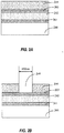
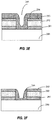
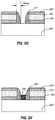
Figures 2A through 2L are simplified cross-sectional views of intermediate structures at different stages of a semiconductor device manufacturing method according to an embodiment of the present invention.Figure 3 is a flowchart of a method for manufacturing a semiconductor device according to an embodiment of the present invention. - With reference to
Figures 2A-2L andFigure 3 , a method for manufacturing a semiconductor device according to an embodiment of the present invention will be described in detail. The method may include the following steps: - Step 101: providing a
semiconductor substrate 200; forming a firstdielectric layer 201 having a first thickness onsemiconductor substrate 200; forming ahardmask layer 202 on firstdielectric layer 201, ananti-reflection layer 203 onhardmask layer 202; and forming aphotoresist layer 204 onanti-reflection layer 203, as shown inFigure 2A . -
Semiconductor substrate 200 may be one of Si, Ge, SiGe, SiGeC, InAs, GaAs, InP, or III/V compound semiconductors.Semiconductor substrate 200 may include a multilayer structure, silicon-on-insulator (SOI), stacked silicon-on-insulator (SSOI), stacked SiGe on insulator (S-SiGeOI), SiGeOI, and GeOI, and combinations thereof. Other devices may also be formed on the semiconductor substrate, such as NMOS and/or PMOS transistors. Further, a conducting structure may also be formed in the semiconductor substrate, e.g., the conducting structure may be a transistor gate, source or drain, and/or a metal interconnect structure may be formed to connect to transistors and other devices. In addition, an isolation structure, e.g., a shallow trench isolation (STI) structure or a local oxidation of silicon (LOCOS) isolation structure can be formed in the semiconductor substrate. In the embodiment of the present invention, the semiconductor substrate includes a single crystal material having a thickness of 1000 nm to 2000 nm. - First
dielectric layer 201 is an insulation layer, such as a gate oxide layer, firstdielectric layer 201 may be made of any suitable insulating material. Firstdielectric layer 201 has a first thickness, which depends from design requirements and applications of the device. In the embodiment, firstdielectric layer 201 is a gate oxide layer comprising silicon dioxide having a thickness of 45 nm. Firstdielectric layer 201 may be formed using conventional deposition processes, such as physical vapor deposition (PVD), chemical vapor deposition (CVP), atomic layer deposition (ALD), and thermal oxidation processes. In an exemplary embodiment, a thermal oxidation process is used to form a silicon dioxide layer for firstdielectric layer 201 or a gate oxide layer. -
Hardmask layer 202 andanti-reflection layer 203 may be formed using any suitable material. In the embodiment,hardmask layer 202 is made of silicon nitride having a thickness of 150 nm,anti-refection layer 203 is made of silicon oxynitride having a thickness of 15 nm, which can reduce the reflection of the silicon nitride layer in a subsequent lithography process, thereby improving the accuracy of the lithography process. -
Photoresist layer 204 may be any suitable positive or negative photoresist material, and its thickness depends from application requirements and can be in the range of 5000 Å to 7000 Å. - Step 102: patterning
photoresist layer 204 to define a first opening having afirst width 205. As shown inFigure 2B ,photoresist layer 204 may be patterned using a conventional photolithographic process, such as exposure, development and other operations to formfirst opening 205 with a first width. The width of the first opening is relatively large, so that existing photolithographic equipment and technology can be used to lower the process cost. In an exemplary embodiment, the first width of the first opening is 450 nm. - Step 103: performing an etching process on
anti-reflection layer 203,hardmask layer 202, and firstdielectric layer 201 using the patterned photoresist layer as a mask. The pattern of patternedphotoresist layer 204 is transferred toanti-reflection layer 203,hardmask layer 202, and firstdielectric layer 201, as shown inFigure 2C .
In the embodiment, the etching process may be a dry etching process, which may include, but is not limited to, reactive ion etching (RIE), ion beam etching, plasma etching, or laser cutting. The dry etching source gases may include CF4, CHF3, or other fluorocarbon containing etching gases.
In an exemplary embodiment, the dry etching process is performed with an etching gas including CF4 or CHF3, at a respective flow rate of 50 sccm to 500 sccm or 10 sccm to 100 sccm, and under a pressure of about 2 mTorr to about 50 mTorr.
It is appreciated that, in the embodiment, the etching ofanti-reflection layer 203,hardmask layer 202, and firstdielectric layer 201 can be conducted in three etching steps, where an appropriate etching gas and etching process parameters are chosen for each step according to the materials used in the respective anti-reflection layer, hardmask layer, and first dielectric layer.
Further, in the embodiment, in order to prevent any damage to the semiconductor substrate during the etching process, when etching firstdielectric layer 201, only a portion of the thickness and not the entire thickness of the first dielectric layer is removed to protectsemiconductor substrate 200. In an exemplary embodiment, a thickness of about 100 Å of firstdielectric layer 201 is retained infirst opening 205 to prevent any damage to the semiconductor substrate caused by the etching process atstep 203. - Step 104: removing the remaining portion of the thickness of first
dielectric layer 201 infirst opening 205 to form a structure as shown inFigure 2D .
In an exemplary embodiment, the remaining portion of firstdielectric layer 201 infirst opening 205 can be removed using a buffered oxide etchant (BOE) solution to form an opening having a first width exposing a surface ofsemiconductor substrate 200. The buffered oxide etchant solution can be formed of a mixture of HF and NH4F with suitable proportions. HF is the main etchant component, and NH4F is used as a buffer to determine the etchant concentration according specific requirements.
In addition, after performingstep 104, the method may include removingphotoresist layer 204 using conventional dry or wet etching techniques, which may include ashing or solvent removal technique. - Step 105: forming a
spacer material layer 206 having a predetermined thickness on the exposed surface of the semiconductor substrate and sidewalls offirst opening 205 to obtain a structure as shown inFigure 2E .
In an exemplary embodiment,spacer material layer 206 is an oxide. In the embodiment, a PECVD TEOS process is used to formspacer material layer 206 having a predetermined thickness on the bottom and sidewalls offirst opening 205. The thickness ofspacer material layer 206 determines the dimension of a subsequently formed tunnel oxide layer, which will be described in detail below. In a specific embodiment, the thickness ofspacer material layer 206 is about 1700 Å.
It is appreciated that the predetermined thickness ofspacer material layer 206 refers to the thickness ofspacer material layer 206 disposed on the bottom offirst opening 205 and on the top surface ofanti-reflection layer 203, or the thickness ofspacer material layer 206 disposed on the sidewalls offirst opening 205 is greater than the predetermined thickness. In other words, if the predetermined thickness is 1700 Å, then the thickness in the middle (center) region offirst opening 205 and the thickness on the top surface ofanti-reflection layer 203 each are 1700 Å, the thickness ofspacer material layer 206 disposed on the sidewalls offirst opening 205 is greater than 1700 Å. - Step 106: removing a portion of the thickness of
spacer material layer 206 by etching to form a structure as shown inFigure 2F .
Referring toFigure 2F , a portion of the thickness ofspacer material layer 206 may be removed, such as 1500 Å from the predetermined thickness of 1700 Å.
It is appreciated that, because the thickness ofspacer material layer 206 on the sidewalls is greater than the predetermined thickness, when a thickness 1600 Å of the spacer material layer on the middle portion offirst opening 205 is removed, a sufficient thickness of the spacer material layer is still remained on the sidewalls offirst opening 205.
In addition, in order to prevent damage to the substrate during etching, a portion of the thickness ofspacer material layer 206 is retained, such as a thickness of 100 Å of the spacer material layer is retained. Afterstep 206, the spacer material layer in the middle region of the first opening has a thickness of about 100 Å, and the spacer material layer on the sidewalls of the first opening has a thickness greater than 100 Å. - Step 107: removing the thickness of the spacer material layer disposed in the middle region of the first opening to form a structure as shown in
Figure 2G .
In an exemplary embodiment, the portion of the spacer material layer disposed in the middle region of the first opening may be removed using a buffered oxide etchant (BOE) solution, which also removes a certain thickness of the spacer material layer disposed on the sidewalls. For example, a thickness of 90 Å of the spacer material layer on the sidewalls is remained to form aspacer 207 while the spacer material layer in the middle region of the first opening is removed.
It is appreciated that the width ofspacer 207 is related to the thickness ofspacer material layer 206, or, described differently, the width of the middle region infirst opening 205 having the predetermined thickness of the spacer material layer and the thickness ofspacer material layer 206 are related to each other. Those skilled in the art may determine the required width ofspacer 207 based on the predetermined thickness ofspacer material layer 206 infirst opening 206 and the amount of the spacer material layer that needs to be etched insteps - Step 108: forming a
second dielectric layer 208 having a second thickness infirst opening 205.
In an exemplary embodiment,second dielectric layer 208 is an oxide that can be formed (a thermally grown oxide layer) onsemiconductor substrate 200 in a thermal furnace. The thickness of seconddielectric layer 208 is about 400 Å according to one embodiment. It is appreciated that the thickness of seconddielectric layer 208 can be determined according to application requirements. In the embodiment, the thickness of seconddielectric layer 208 is smaller than the thickness of firstdielectric layer 201, i.e., the second thickness is smaller than the first thickness. In some embodiments, the second thickness may be greater than or equal to the first thickness. - Step 109: removing
spacer 207 on the sidewalls offirst opening 205 to form asecond opening 209 having a second width, as shown in a structure ofFigure 2I .
In the embodiment, an HF solution having a ratio of HF (hydrofluoric acid) to water of about 50:1 is used to removespacer 207 on the sidewalls offirst opening 205, because the concentration ratio of the 50:1 HF solution and the etch rate ratio of TEOS to the thermal oxide is about 10:1,spacer 207 can be completely removed using the concentration ratio of HF to water of about 50:1, thereby ensuring that the thermal oxide layer in the middle region of a channel has a sufficient thickness. In the embodiment,second dielectric layer 208 has a thickness of about 300 Å after the wet etching process.
It is appreciated that, althoughspacer 207 includes TEOS and seconddielectric layer 208 includes a thermal silicon oxide layer in the example embodiment, other suitable materials may also be used, as long as the spacer has a high etching selectivity relative to the second dielectric layer so that the second dielectric layer will not suffer any damage when the spacer is removed. - Step 110: removing
anti-reflection layer 203 andhardmask layer 202 to form a second opening having afirst portion 209a and a second portion 209b adjacent seconddielectric layer 208, the first and second portion each have a second width that is smaller than the first width, as shown inFigure 2J .
In an exemplary embodiment,anti-reflection layer 203 andhardmask layer 202 can be removed by wet etching, for example, using phosphoric acid solutions. - Step 111: forming a third
dielectric layer 210 on the second opening having the second width, as shown inFigure 2K .
In the embodiment, an oxide layer may be formed using an in-situ steam growth (ISSG) process on the second opening to form thirddielectric layer 210 having a third thickness. In an example embodiment, the third thickness is about 80 Å.
It is appreciated that the thickness of thirddielectric layer 210 is smaller than the thickness of firstdielectric layer 201 and the thickness of seconddielectric layer 208. However, the thickness of thirddielectric layer 210 is not limited to 80 Å and can have other dimension depending from applications or design requirements. Since the thickness of thirddielectric layer 210 is smaller than the thickness of firstdielectric layer 201 and the thickness of seconddielectric layer 208, the third dielectric layer is divided into two portions by seconddielectric layer 208, as shown inFigure 2K . - Step 112: forming a
gate material layer 211 over one portion of thirddielectric layer 210.
In an exemplary embodiment,gate material layer 211 may be formed using convention deposition processes, such as PVD, CVD, ALD, and the like. - It is appreciated that, since the gap between the two portions of the third dielectric layer is narrow, one portion of the third dielectric layers can be used as a tunneling oxide layer, and a floating gate can be formed thereon, in order to prevent that, in the case after the tunneling oxide layer is formed, a dielectric layer cannot be formed subsequently between the floating gates on the two tunneling oxide layers.
- This completes the process steps of the manufacturing method according to some embodiments of the present invention. It is understood that that the above-described method may include other steps other than the above-described steps, such as forming ONN layers or control gate layers, forming source/drain, and other steps that are also included within the scope of the present invention.
- Embodiments of the present invention provide a
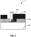
semiconductor device 4, as shown inFigure 4 .Semiconductor device 4 may include asemiconductor substrate 400, a firstdielectric layer 401 having a first thickness onsemiconductor substrate 400, afirst opening 402 having a first width in firstdielectric layer 401, asecond dielectric layer 403 having a second thickness disposed in a middle region offirst opening 402, and a thirddielectric layer 404 having a first portion and a second portion disposed on opposite sides of seconddielectric layer 403.Third dielectric layer 404 has a third thickness that is smaller than the first thickness of firstdielectric layer 401 and the second thickness of second dielectric layer 408. The width of the first and second portions of thirddielectric layer 404 is smaller than the first width offirst opening 402. -
Semiconductor device 4 further includes agate material layer 405 over the first portion of thirddielectric layer 403. -
Semiconductor substrate 400 may be one of Si, Ge, SiGe, SiC, SiGeC, InAs, GaAs, InP, or III/V compound semiconductor materials.Semiconductor substrate 400 may also include a multilayer structure, silicon-on-insulator (SOI), stacked silicon-on-insulator (SSOI), stacked SiGe on insulator (S-SiGeOI), SiGeOI, and GeOi, and combinations thereof.Semiconductor substrate 400 may further include other devices, such as NMOS and/or PMOS transistors. In addition,semiconductor substrate 400 may also include a conducting structure, such as a transistor gate, source or drain, and/or a metal interconnect structure configured to connect transistors and other devices to each other. In addition,semiconductor substrate 400 may also include an isolation structure, e.g., a shallow trench isolation (STI) structure or a local oxidation of silicon (LOCOS) isolation structure. In the embodiment of the present invention, the semiconductor substrate includes a single crystal material. - First, second, third
dielectric layers Gate material layer 405 may be a polysilicon formed by PVD, CVD, ALD, and other conventional deposition processes. - Embodiments of the present invention also provide an electronic device, which may include an electronic component and a semiconductor device electrically connected to the electronic component. The semiconductor device can be manufactured according to the above-described method.
- In an embodiment, the semiconductor device may include a semiconductor substrate, a first dielectric layer having a first thickness on semiconductor substrate, a first opening having a first width in first dielectric layer, a second dielectric layer having a second thickness disposed in a middle region of first opening, and a third dielectric layer having a first portion and a second portion disposed on opposite sides of second dielectric layer. The third dielectric layer has a third thickness that is smaller than the first thickness of the first dielectric layer and the second thickness of the second dielectric layer. The width of the first and second portions of third dielectric layer is smaller than the first width of the first opening.
- The semiconductor device further includes a gate material layer disposed over the first portion of the third dielectric layer.
- The semiconductor substrate may be one of Si, Ge, SiGe, SiC, SiGeC, InAs, GaAs, InP, or III/V compound semiconductor materials. The semiconductor substrate may also include a multilayer structure, silicon-on-insulator (SOI), stacked silicon-on-insulator (SSOI), stacked SiGe on insulator (S-SiGeOI), SiGeOI, and GeOi, and combinations thereof. The semiconductor substrate may further include other devices, such as NMOS and/or PMOS transistors. In addition, the semiconductor substrate may also include a conducting structure, such as a transistor gate, source or drain, and/or a metal interconnect structure configured to connect transistors and other devices to each other. In addition, the semiconductor substrate may also include an isolation structure, e.g., a shallow trench isolation (STI) structure or a local oxidation of silicon (LOCOS) isolation structure. In the embodiment of the present invention, the semiconductor substrate includes a single crystal material.
- The first, second, and third dielectric layers may include an oxide, such as silicon dioxide, that can be formed using PECVD, TEOS, ISSG or thermal oxide forming techniques. The gate material layer may be of a polysilicon layer formed by PVD, CVD, ALD, and other conventional deposition processes.
- In an embodiment, the electronic device may include a semiconductor device fabricated using the above-described method. The electronic device may be a mobile phone, a laptop, a netbook, a tablet PC, a game console, a TV, a DVD player, a GPS device, a camera, a voice recorder, MP3 player, MP4 player, PSP player, and other semiconductor devices including intermediate products and electronic components that are manufactured using the above-described method to have the above-described cost advantages.
- While the present invention is described herein with reference to illustrative embodiments, this description is not intended to be construed in a limiting sense. Rather, the purpose of the illustrative embodiments is to make the spirit of the present invention be better understood by those skilled in the art. In order not to obscure the scope of the invention, many details of well-known processes and manufacturing techniques are omitted. Various modifications of the illustrative embodiments as well as other embodiments will be apparent to those of skill in the art upon reference to the description.
Claims (14)
- A method for manufacturing a semiconductor device comprising:providing a semiconductor substrate;forming a first dielectric layer having a first thickness on the semiconductor substrate;forming a first opening having a first width in the first dielectric layer, the first opening exposing a surface of the semiconductor substrate;forming a spacer on opposite sidewalls of the first opening;forming a second dielectric layer having a second thickness on the exposed surface of the semiconductor substrate in a middle region of the first opening;removing the spacer to form a second opening having a first opening portion and a second opening portion on opposite sides of the second dielectric layer, each of the first and second opening portions having a second width;forming a third dielectric layer having a third thickness on the first and second opening portions of the second opening, the third thickness being smaller than the first thickness and the second thickness.
- The method of claim 1, wherein forming the first opening comprises:forming a hardmask layer on the first dielectric layer;forming an anti-reflection layer on the hardmask layer;forming a third opening having the first width in the hardmask layer and the anti-reflection layer; andperforming an etching process on the first dielectric layer using the hardmask layer and the anti-reflection layer as a mask.
- The method of claim 1 or 2, wherein performing the etching process comprises:performing a dry etching process to remove a portion of the first thickness of the first dielectric layer while retaining a remaining portion of the first thickness of the first dielectric layer;removing the remaining portion of the first thickness of the first dielectric layer using a first buffered oxide etchant,, BOE, solution.
- The method of any one of the claims 1-3, wherein forming the spacer comprises:forming a spacer material layer having a thickness on a bottom and on sidewalls of the first opening;removing the spacer material layer on the bottom of the first opening.
- The method of claim 4, wherein removing the spacer material layer on the bottom of the first opening comprises:removing a portion of the thickness of the spacer material layer on the bottom of the first opening while retaining a remaining portion of the thickness of the spacer material layer; andremoving the remaining portion of the thickness of the spacer material layer using a second buffered oxide etchant (BOE) solution.
- The method of any one of the claims 1-5, further comprising:forming a gate material layer on the third dielectric layer.
- The method of claim 6, wherein the gate material layer covers a portion of the third dielectric layer disposed on one of the first and second opening portions of the second opening.
- The method of claim 5 or 6, wherein the third dielectric layer is a tunneling oxide layer, and the gate material layer is a floating gate.
- The method of any one of the claims 1-8, wherein the second thickness is smaller than the first thickness.
- The method of any one of the claims 1-9, wherein the spacer has a high etching selectivity relative to the second dielectric layer.
- A semiconductor device comprising:a semiconductor substrate;a first dielectric layer having a first thickness on the semiconductor substrate;a first opening having a first width in the first dielectric layer;a second dielectric layer having a second thickness disposed in a middle region of the first opening; anda third dielectric layer having a first portion and a second portion disposed on opposite sides of second dielectric layer, the first portion and the second portion having a second width smaller than the first width, and the third dielectric layer having a third thickness smaller than the first thickness and the second thickness.
- The semiconductor device of claim 11, further comprising:a gate material layer on the third dielectric layer.
- The semiconductor device of claim 12, wherein the gate material layer is disposed on one of the first and second portions of the third dielectric layer.
- An electronic device comprising a semiconductor device of any one of the claims 11-13 and an electronic component connected to the semiconductor device.
Applications Claiming Priority (1)
| Application Number | Priority Date | Filing Date | Title |
|---|---|---|---|
| CN201610017721.2A CN106972021B (en) | 2016-01-12 | 2016-01-12 | A kind of semiconductor device and its manufacturing method, electronic device |
Publications (1)
| Publication Number | Publication Date |
|---|---|
| EP3193354A1 true EP3193354A1 (en) | 2017-07-19 |
Family
ID=57755202
Family Applications (1)
| Application Number | Title | Priority Date | Filing Date |
|---|---|---|---|
| EP17150399.8A Withdrawn EP3193354A1 (en) | 2016-01-12 | 2017-01-05 | Method of manufacturing an eeprom device |
Country Status (3)
| Country | Link |
|---|---|
| US (2) | US10079241B2 (en) |
| EP (1) | EP3193354A1 (en) |
| CN (1) | CN106972021B (en) |
Cited By (1)
| Publication number | Priority date | Publication date | Assignee | Title |
|---|---|---|---|---|
| WO2019200582A1 (en) * | 2018-04-19 | 2019-10-24 | Yangtze Memory Technologies Co., Ltd. | Memory device and forming method thereof |
Families Citing this family (4)
| Publication number | Priority date | Publication date | Assignee | Title |
|---|---|---|---|---|
| CN106972021B (en) | 2016-01-12 | 2019-12-13 | 中芯国际集成电路制造(上海)有限公司 | A kind of semiconductor device and its manufacturing method, electronic device |
| US10861706B2 (en) * | 2018-10-26 | 2020-12-08 | Taiwan Semiconductor Manufacturing Co., Ltd. | Etch selectivity improved by laser beam |
| US11404417B2 (en) | 2020-02-26 | 2022-08-02 | Taiwan Semiconductor Manufacturing Co., Ltd. | Low leakage device |
| US11641739B2 (en) * | 2020-06-01 | 2023-05-02 | Globalfoundries Singapore Pte. Ltd. | Semiconductor non-volatile memory devices |
Citations (5)
| Publication number | Priority date | Publication date | Assignee | Title |
|---|---|---|---|---|
| FR2855325A1 (en) * | 2003-05-20 | 2004-11-26 | Samsung Electronics Co Ltd | Electrically erasable programmable read only memory cell structure for smart card, has memory transistor with gate having dielectric layer defining adjacent channel region with thickness greater than tunnel region thickness |
| US20050051835A1 (en) * | 2003-05-20 | 2005-03-10 | Kang Sung-Taeg | EEPROM device for increasing a coupling ratio and fabrication method thereof |
| US20050208744A1 (en) * | 2004-03-18 | 2005-09-22 | Samsung Electronics Co., Ltd. | Split gate type nonvolatile semiconductor memory device, and method of fabricating the same |
| US20090014773A1 (en) * | 2007-07-10 | 2009-01-15 | Ching-Nan Hsiao | Two bit memory structure and method of making the same |
| US20090186460A1 (en) * | 2008-01-21 | 2009-07-23 | Stmicroelectronics (Rousset) Sas | Method for manufacturing an eeprom cell |
Family Cites Families (11)
| Publication number | Priority date | Publication date | Assignee | Title |
|---|---|---|---|---|
| JP5191633B2 (en) * | 2006-04-04 | 2013-05-08 | ルネサスエレクトロニクス株式会社 | Semiconductor device and manufacturing method thereof |
| JP4829015B2 (en) * | 2006-06-20 | 2011-11-30 | 株式会社東芝 | Nonvolatile semiconductor memory device |
| US7948021B2 (en) * | 2007-04-27 | 2011-05-24 | Kabushiki Kaisha Toshiba | Semiconductor memory device and method of fabricating the same |
| US8390079B2 (en) * | 2010-10-28 | 2013-03-05 | International Business Machines Corporation | Sealed air gap for semiconductor chip |
| JP2013065777A (en) * | 2011-09-20 | 2013-04-11 | Toshiba Corp | Semiconductor device and manufacturing method of semiconductor device |
| KR101906167B1 (en) * | 2011-10-27 | 2018-10-12 | 삼성전자주식회사 | Nonvolatile memory device and and fabricating method thereof |
| US8564068B2 (en) * | 2012-01-05 | 2013-10-22 | Taiwan Semiconductor Manufacturing Company, Ltd. | Device and methods for small trench patterning |
| CN104067392B (en) * | 2012-04-30 | 2016-10-26 | 惠普发展公司,有限责任合伙企业 | Including the device enlivening floating gate region area less than channel area |
| KR101891777B1 (en) * | 2012-06-25 | 2018-08-24 | 삼성전자주식회사 | Light emitting device having dielectric reflector and method of manufacturing the same |
| KR101926027B1 (en) * | 2012-08-31 | 2018-12-06 | 에스케이하이닉스 주식회사 | Semiconductor device having asymmetry bit line contact and method for manufacturing the same |
| CN106972021B (en) | 2016-01-12 | 2019-12-13 | 中芯国际集成电路制造(上海)有限公司 | A kind of semiconductor device and its manufacturing method, electronic device |
-
2016
- 2016-01-12 CN CN201610017721.2A patent/CN106972021B/en active Active
- 2016-11-28 US US15/362,551 patent/US10079241B2/en active Active
-
2017
- 2017-01-05 EP EP17150399.8A patent/EP3193354A1/en not_active Withdrawn
-
2018
- 2018-08-14 US US16/103,725 patent/US10483269B2/en active Active
Patent Citations (5)
| Publication number | Priority date | Publication date | Assignee | Title |
|---|---|---|---|---|
| FR2855325A1 (en) * | 2003-05-20 | 2004-11-26 | Samsung Electronics Co Ltd | Electrically erasable programmable read only memory cell structure for smart card, has memory transistor with gate having dielectric layer defining adjacent channel region with thickness greater than tunnel region thickness |
| US20050051835A1 (en) * | 2003-05-20 | 2005-03-10 | Kang Sung-Taeg | EEPROM device for increasing a coupling ratio and fabrication method thereof |
| US20050208744A1 (en) * | 2004-03-18 | 2005-09-22 | Samsung Electronics Co., Ltd. | Split gate type nonvolatile semiconductor memory device, and method of fabricating the same |
| US20090014773A1 (en) * | 2007-07-10 | 2009-01-15 | Ching-Nan Hsiao | Two bit memory structure and method of making the same |
| US20090186460A1 (en) * | 2008-01-21 | 2009-07-23 | Stmicroelectronics (Rousset) Sas | Method for manufacturing an eeprom cell |
Cited By (5)
| Publication number | Priority date | Publication date | Assignee | Title |
|---|---|---|---|---|
| WO2019200582A1 (en) * | 2018-04-19 | 2019-10-24 | Yangtze Memory Technologies Co., Ltd. | Memory device and forming method thereof |
| US10910390B2 (en) | 2018-04-19 | 2021-02-02 | Yangtze Memory Technologies Co., Ltd. | Memory device and forming method thereof |
| US11211393B2 (en) | 2018-04-19 | 2021-12-28 | Yangtze Memory Technologies Co., Ltd. | Memory device and forming method thereof |
| US11271004B2 (en) | 2018-04-19 | 2022-03-08 | Yangtze Memory Technologies Co., Ltd. | Memory device and forming method thereof |
| US11380701B2 (en) | 2018-04-19 | 2022-07-05 | Yangtze Memory Technologies Co., Ltd. | Memory device and forming method thereof |
Also Published As
| Publication number | Publication date |
|---|---|
| US20180366480A1 (en) | 2018-12-20 |
| US20170200728A1 (en) | 2017-07-13 |
| CN106972021A (en) | 2017-07-21 |
| CN106972021B (en) | 2019-12-13 |
| US10483269B2 (en) | 2019-11-19 |
| US10079241B2 (en) | 2018-09-18 |
Similar Documents
| Publication | Publication Date | Title |
|---|---|---|
| US10998235B2 (en) | FinFET with sloped surface at interface between isolation structures and manufacturing method thereof | |
| US10483269B2 (en) | EEPROM device | |
| US9704974B2 (en) | Process of manufacturing Fin-FET device | |
| US9685382B1 (en) | Method for reducing loss of silicon cap layer over SiGe source/drain in a CMOS device | |
| US10340271B2 (en) | Semiconductor structure and fabrication method thereof | |
| CN115050631A (en) | Semiconductor device and method for manufacturing the same | |
| US9214392B1 (en) | Method of forming contact hole and semiconductor structure with contact plug | |
| KR20060092857A (en) | A semiconductor device having an etch resistant L-type spacer and a method of manufacturing the same | |
| US20210020518A1 (en) | Semiconductor structure | |
| CN106601678A (en) | Semiconductor device, preparation method therefor, and electronic device | |
| US9660058B2 (en) | Method of FinFET formation | |
| CN104916639A (en) | Semi-floating gate memory structure and manufacturing method thereof | |
| CN108735670B (en) | A semiconductor device and its manufacturing method and electronic device | |
| CN108010835A (en) | A kind of semiconductor devices and preparation method thereof, electronic device | |
| US9917210B1 (en) | FinFET transistor gate and epitaxy formation | |
| CN111162044B (en) | Manufacturing method of semiconductor device, semiconductor device and electronic device | |
| CN106611708A (en) | Semiconductor device, preparation method thereof and electronic device | |
| CN107978563B (en) | Semiconductor device, preparation method and electronic device | |
| CN111180450B (en) | A kind of semiconductor device and its manufacturing method, electronic device | |
| US9337104B1 (en) | Method for chemical mechanical polishing of high-K metal gate structures | |
| CN106910706B (en) | Method for manufacturing semiconductor device | |
| CN104078362A (en) | Semiconductor device manufacturing method | |
| US20050090088A1 (en) | Method for forming a word line spacer with good square profile | |
| KR100843014B1 (en) | Manufacturing Method of Semiconductor Device | |
| CN120857506A (en) | Method for manufacturing semiconductor structure |
Legal Events
| Date | Code | Title | Description |
|---|---|---|---|
| PUAI | Public reference made under article 153(3) epc to a published international application that has entered the european phase |
Free format text: ORIGINAL CODE: 0009012 |
|
| STAA | Information on the status of an ep patent application or granted ep patent |
Free format text: STATUS: THE APPLICATION HAS BEEN PUBLISHED |
|
| AK | Designated contracting states |
Kind code of ref document: A1 Designated state(s): AL AT BE BG CH CY CZ DE DK EE ES FI FR GB GR HR HU IE IS IT LI LT LU LV MC MK MT NL NO PL PT RO RS SE SI SK SM TR |
|
| AX | Request for extension of the european patent |
Extension state: BA ME |
|
| RAP1 | Party data changed (applicant data changed or rights of an application transferred) |
Owner name: SEMICONDUCTOR MANUFACTURING INTERNATIONAL CORPORAT |
|
| STAA | Information on the status of an ep patent application or granted ep patent |
Free format text: STATUS: REQUEST FOR EXAMINATION WAS MADE |
|
| 17P | Request for examination filed |
Effective date: 20180109 |
|
| RBV | Designated contracting states (corrected) |
Designated state(s): AL AT BE BG CH CY CZ DE DK EE ES FI FR GB GR HR HU IE IS IT LI LT LU LV MC MK MT NL NO PL PT RO RS SE SI SK SM TR |
|
| RAP1 | Party data changed (applicant data changed or rights of an application transferred) |
Owner name: SEMICONDUCTOR MANUFACTURING INTERNATIONAL (BEIJING Owner name: SEMICONDUCTOR MANUFACTURING INTERNATIONAL (SHANGHA |
|
| STAA | Information on the status of an ep patent application or granted ep patent |
Free format text: STATUS: EXAMINATION IS IN PROGRESS |
|
| 17Q | First examination report despatched |
Effective date: 20181114 |
|
| STAA | Information on the status of an ep patent application or granted ep patent |
Free format text: STATUS: THE APPLICATION IS DEEMED TO BE WITHDRAWN |
|
| 18D | Application deemed to be withdrawn |
Effective date: 20210806 |