EP3188276A1 - Organic light-emitting diode display device - Google Patents
Organic light-emitting diode display device Download PDFInfo
- Publication number
- EP3188276A1 EP3188276A1 EP16207237.5A EP16207237A EP3188276A1 EP 3188276 A1 EP3188276 A1 EP 3188276A1 EP 16207237 A EP16207237 A EP 16207237A EP 3188276 A1 EP3188276 A1 EP 3188276A1
- Authority
- EP
- European Patent Office
- Prior art keywords
- light
- layer
- emitting
- thickness
- display device
- Prior art date
- Legal status (The legal status is an assumption and is not a legal conclusion. Google has not performed a legal analysis and makes no representation as to the accuracy of the status listed.)
- Granted
Links
Images




Classifications
-
- H—ELECTRICITY
- H10—SEMICONDUCTOR DEVICES; ELECTRIC SOLID-STATE DEVICES NOT OTHERWISE PROVIDED FOR
- H10K—ORGANIC ELECTRIC SOLID-STATE DEVICES
- H10K50/00—Organic light-emitting devices
- H10K50/80—Constructional details
- H10K50/85—Arrangements for extracting light from the devices
- H10K50/852—Arrangements for extracting light from the devices comprising a resonant cavity structure, e.g. Bragg reflector pair
-
- H—ELECTRICITY
- H10—SEMICONDUCTOR DEVICES; ELECTRIC SOLID-STATE DEVICES NOT OTHERWISE PROVIDED FOR
- H10K—ORGANIC ELECTRIC SOLID-STATE DEVICES
- H10K50/00—Organic light-emitting devices
- H10K50/10—OLEDs or polymer light-emitting diodes [PLED]
- H10K50/14—Carrier transporting layers
- H10K50/15—Hole transporting layers
-
- H—ELECTRICITY
- H10—SEMICONDUCTOR DEVICES; ELECTRIC SOLID-STATE DEVICES NOT OTHERWISE PROVIDED FOR
- H10K—ORGANIC ELECTRIC SOLID-STATE DEVICES
- H10K50/00—Organic light-emitting devices
- H10K50/10—OLEDs or polymer light-emitting diodes [PLED]
- H10K50/17—Carrier injection layers
-
- H—ELECTRICITY
- H10—SEMICONDUCTOR DEVICES; ELECTRIC SOLID-STATE DEVICES NOT OTHERWISE PROVIDED FOR
- H10K—ORGANIC ELECTRIC SOLID-STATE DEVICES
- H10K59/00—Integrated devices, or assemblies of multiple devices, comprising at least one organic light-emitting element covered by group H10K50/00
- H10K59/10—OLED displays
- H10K59/12—Active-matrix OLED [AMOLED] displays
- H10K59/122—Pixel-defining structures or layers, e.g. banks
-
- H—ELECTRICITY
- H10—SEMICONDUCTOR DEVICES; ELECTRIC SOLID-STATE DEVICES NOT OTHERWISE PROVIDED FOR
- H10K—ORGANIC ELECTRIC SOLID-STATE DEVICES
- H10K59/00—Integrated devices, or assemblies of multiple devices, comprising at least one organic light-emitting element covered by group H10K50/00
- H10K59/30—Devices specially adapted for multicolour light emission
-
- H—ELECTRICITY
- H10—SEMICONDUCTOR DEVICES; ELECTRIC SOLID-STATE DEVICES NOT OTHERWISE PROVIDED FOR
- H10K—ORGANIC ELECTRIC SOLID-STATE DEVICES
- H10K59/00—Integrated devices, or assemblies of multiple devices, comprising at least one organic light-emitting element covered by group H10K50/00
- H10K59/80—Constructional details
- H10K59/875—Arrangements for extracting light from the devices
- H10K59/876—Arrangements for extracting light from the devices comprising a resonant cavity structure, e.g. Bragg reflector pair
-
- G—PHYSICS
- G02—OPTICS
- G02F—OPTICAL DEVICES OR ARRANGEMENTS FOR THE CONTROL OF LIGHT BY MODIFICATION OF THE OPTICAL PROPERTIES OF THE MEDIA OF THE ELEMENTS INVOLVED THEREIN; NON-LINEAR OPTICS; FREQUENCY-CHANGING OF LIGHT; OPTICAL LOGIC ELEMENTS; OPTICAL ANALOGUE/DIGITAL CONVERTERS
- G02F1/00—Devices or arrangements for the control of the intensity, colour, phase, polarisation or direction of light arriving from an independent light source, e.g. switching, gating or modulating; Non-linear optics
- G02F1/01—Devices or arrangements for the control of the intensity, colour, phase, polarisation or direction of light arriving from an independent light source, e.g. switching, gating or modulating; Non-linear optics for the control of the intensity, phase, polarisation or colour
- G02F1/13—Devices or arrangements for the control of the intensity, colour, phase, polarisation or direction of light arriving from an independent light source, e.g. switching, gating or modulating; Non-linear optics for the control of the intensity, phase, polarisation or colour based on liquid crystals, e.g. single liquid crystal display cells
- G02F1/133—Constructional arrangements; Operation of liquid crystal cells; Circuit arrangements
- G02F1/136—Liquid crystal cells structurally associated with a semi-conducting layer or substrate, e.g. cells forming part of an integrated circuit
- G02F1/1362—Active matrix addressed cells
- G02F1/136222—Colour filters incorporated in the active matrix substrate
-
- H—ELECTRICITY
- H10—SEMICONDUCTOR DEVICES; ELECTRIC SOLID-STATE DEVICES NOT OTHERWISE PROVIDED FOR
- H10F—INORGANIC SEMICONDUCTOR DEVICES SENSITIVE TO INFRARED RADIATION, LIGHT, ELECTROMAGNETIC RADIATION OF SHORTER WAVELENGTH OR CORPUSCULAR RADIATION
- H10F39/00—Integrated devices, or assemblies of multiple devices, comprising at least one element covered by group H10F30/00, e.g. radiation detectors comprising photodiode arrays
- H10F39/10—Integrated devices
- H10F39/12—Image sensors
- H10F39/18—Complementary metal-oxide-semiconductor [CMOS] image sensors; Photodiode array image sensors
- H10F39/182—Colour image sensors
-
- H—ELECTRICITY
- H10—SEMICONDUCTOR DEVICES; ELECTRIC SOLID-STATE DEVICES NOT OTHERWISE PROVIDED FOR
- H10K—ORGANIC ELECTRIC SOLID-STATE DEVICES
- H10K2102/00—Constructional details relating to the organic devices covered by this subclass
- H10K2102/301—Details of OLEDs
- H10K2102/351—Thickness
-
- H—ELECTRICITY
- H10—SEMICONDUCTOR DEVICES; ELECTRIC SOLID-STATE DEVICES NOT OTHERWISE PROVIDED FOR
- H10K—ORGANIC ELECTRIC SOLID-STATE DEVICES
- H10K50/00—Organic light-emitting devices
- H10K50/10—OLEDs or polymer light-emitting diodes [PLED]
- H10K50/11—OLEDs or polymer light-emitting diodes [PLED] characterised by the electroluminescent [EL] layers
-
- H—ELECTRICITY
- H10—SEMICONDUCTOR DEVICES; ELECTRIC SOLID-STATE DEVICES NOT OTHERWISE PROVIDED FOR
- H10K—ORGANIC ELECTRIC SOLID-STATE DEVICES
- H10K59/00—Integrated devices, or assemblies of multiple devices, comprising at least one organic light-emitting element covered by group H10K50/00
- H10K59/30—Devices specially adapted for multicolour light emission
- H10K59/35—Devices specially adapted for multicolour light emission comprising red-green-blue [RGB] subpixels
-
- H—ELECTRICITY
- H10—SEMICONDUCTOR DEVICES; ELECTRIC SOLID-STATE DEVICES NOT OTHERWISE PROVIDED FOR
- H10K—ORGANIC ELECTRIC SOLID-STATE DEVICES
- H10K59/00—Integrated devices, or assemblies of multiple devices, comprising at least one organic light-emitting element covered by group H10K50/00
- H10K59/30—Devices specially adapted for multicolour light emission
- H10K59/35—Devices specially adapted for multicolour light emission comprising red-green-blue [RGB] subpixels
- H10K59/352—Devices specially adapted for multicolour light emission comprising red-green-blue [RGB] subpixels the areas of the RGB subpixels being different
-
- H—ELECTRICITY
- H10—SEMICONDUCTOR DEVICES; ELECTRIC SOLID-STATE DEVICES NOT OTHERWISE PROVIDED FOR
- H10K—ORGANIC ELECTRIC SOLID-STATE DEVICES
- H10K59/00—Integrated devices, or assemblies of multiple devices, comprising at least one organic light-emitting element covered by group H10K50/00
- H10K59/30—Devices specially adapted for multicolour light emission
- H10K59/35—Devices specially adapted for multicolour light emission comprising red-green-blue [RGB] subpixels
- H10K59/353—Devices specially adapted for multicolour light emission comprising red-green-blue [RGB] subpixels characterised by the geometrical arrangement of the RGB subpixels
-
- H—ELECTRICITY
- H10—SEMICONDUCTOR DEVICES; ELECTRIC SOLID-STATE DEVICES NOT OTHERWISE PROVIDED FOR
- H10K—ORGANIC ELECTRIC SOLID-STATE DEVICES
- H10K59/00—Integrated devices, or assemblies of multiple devices, comprising at least one organic light-emitting element covered by group H10K50/00
- H10K59/30—Devices specially adapted for multicolour light emission
- H10K59/38—Devices specially adapted for multicolour light emission comprising colour filters or colour changing media [CCM]
-
- H—ELECTRICITY
- H10—SEMICONDUCTOR DEVICES; ELECTRIC SOLID-STATE DEVICES NOT OTHERWISE PROVIDED FOR
- H10K—ORGANIC ELECTRIC SOLID-STATE DEVICES
- H10K85/00—Organic materials used in the body or electrodes of devices covered by this subclass
- H10K85/30—Coordination compounds
- H10K85/341—Transition metal complexes, e.g. Ru(II)polypyridine complexes
- H10K85/342—Transition metal complexes, e.g. Ru(II)polypyridine complexes comprising iridium
-
- H—ELECTRICITY
- H10—SEMICONDUCTOR DEVICES; ELECTRIC SOLID-STATE DEVICES NOT OTHERWISE PROVIDED FOR
- H10K—ORGANIC ELECTRIC SOLID-STATE DEVICES
- H10K85/00—Organic materials used in the body or electrodes of devices covered by this subclass
- H10K85/60—Organic compounds having low molecular weight
- H10K85/649—Aromatic compounds comprising a hetero atom
- H10K85/657—Polycyclic condensed heteroaromatic hydrocarbons
- H10K85/6572—Polycyclic condensed heteroaromatic hydrocarbons comprising only nitrogen in the heteroaromatic polycondensed ring system, e.g. phenanthroline or carbazole
Definitions
- the present disclosure relates to an organic light-emitting diode display device, and more particularly, to an organic light-emitting diode display device capable of improving a lifetime.
- organic light-emitting diode (OLED) display devices which can be referred to as organic electroluminescent display devices, emit light during loss of electron-hole pairs.
- the electron-hole pairs are formed by injecting charges into a light-emitting layer between a cathode for injecting electrons and an anode for injecting holes.
- the OLED display devices can include a flexible substrate such as plastic. Since they are self-luminous, the OLED display devices have excellent contrast ratios. The OLED display devices have a response time of several micro seconds, and there are advantages in displaying moving images. The OLED display devices have wide viewing angles.
- OLED display devices can be passive matrix type OLED display devices and active matrix type OLED display devices.
- Active matrix type display devices have low power consumption and high definition.
- the size of active matrix type display devices can be large.
- An OLED display device includes a plurality of pixels to express various colors.
- Each pixel includes red, green and blue sub-pixels, and red, green and blue organic light-emitting diodes are formed in the red, green and blue sub-pixels, respectively.
- the red, green and blue organic light-emitting diodes include red, green and blue light-emitting material layers, respectively, and each light-emitting material layer is formed by a thermal evaporation method. More particularly, the light-emitting material layer is formed by selectively vacuum evaporating an organic light-emitting material using a fine metal mask.
- the thermal evaporation method is difficult to be applied to display devices having a large size and high definition due to making deviation, sagging and a shadow effect of the mask.
- a method of forming the light-emitting material layer through a solution process has been suggested.
- a bank layer surrounding a pixel region is formed, a light-emitting material is dropped in the pixel region surrounded by the bank layer by scanning a nozzle of injection apparatus in a certain direction, and the dropped light-emitting material is hardened, there by forming the light-emitting material layer.
- a hole injecting layer and a hole transporting layer also may be formed through the solution process.
- the red, green and blue light-emitting materials have different properties.
- the red light-emitting material has relative low efficiency and the green light-emitting material has relatively short lifetime.
- reflection of the external light is high in the OLED display device.
- the reflection of the external light increases the brightness at black state, and the contrast ratio is lowered. Therefore, image qualities are decreased because of the reflection of the external light.
- at least one polarizer is used, and this causes an increase in costs.
- the present disclosure is directed to an OLED display device that substantially obviates one or more of the problems due to limitations and disadvantages of the related art.
- An object of the present disclosure is to provide an OLED display device that increases a lifetime.
- Another object of the present disclosure is to provide an OLED display device that decreases costs.
- an organic light-emitting diode display device includes a substrate on which red, green and blue sub-pixel regions are defined; first electrodes in the red, green and blue sub-pixel regions, respectively; first, second and third light-emitting layers on the corresponding first electrodes and in the red, green and blue sub-pixel regions, respectively; a second electrode on the first, second and third light-emitting layers; and red, green and blue color filters on the second electrode and corresponding to the red, green and blue sub-pixel regions, respectively, wherein a thickness of the first light-emitting layer is smaller than a thickness of the second light emitting layer.
- an organic light-emitting diode display device comprising: a substrate on which red, green and blue sub-pixel regions are defined; a first electrode in each of the red, green and blue sub-pixel regions; first, second and third light-emitting layers on the first electrodes in the red, green and blue sub-pixel regions, respectively, each of the first and second light-emitting layers including a yellow light-emitting material having a first emission peak and a second emission peak different from the first emission peak; a second electrode on the first, second and third light-emitting layers; and red, green and blue color filters on the second electrode and corresponding to the red, green and blue sub-pixel regions, respectively.
- a thickness of the first light-emitting layer is smaller than a thickness of the second light emitting layer.
- an organic light-emitting diode display device wherein each of the first and second light-emitting layers including a yellow light-emitting material having a first emission peak and a second emission peak different from the first emission peak and the thickness of the first light-emitting layer is smaller than a thickness of the second light emitting layer.
- the third light-emitting layer includes a blue light-emitting material.
- a thickness of the third light-emitting layer is smaller than the thickness of the first light-emitting layer
- each of the first and second light-emitting layers includes a yellow light-emitting material.
- the yellow light-emitting material has a first emission peak within a wavelength range of 530 nm to 555 nm and a second emission peak within a wavelength range of 590 nm to 620 nm.
- the yellow light-emitting material includes 4,4'-N,N'-dicarbazole-biphenyl (CBP) and also includes bis[2-(4-tertbutylphenyl)benzothiazolato-N,C2']iridium(acetylactonate)[(t-bt)2Ir(acac)] as a dopant.
- CBP 4,4'-N,N'-dicarbazole-biphenyl
- each of the first and second light-emitting layers include a hole auxiliary layer, a light-emitting material layer and an electron auxiliary layer, and wherein a thickness of the hole auxiliary layer of the first light-emitting layer is smaller than a thickness of the hole auxiliary layer of the second light-emitting layer.
- the thickness of the hole auxiliary layer of the first light-emitting layer corresponds to a second order cavity condition
- the thickness of the hole auxiliary layer of the second light-emitting layer corresponds to a third order cavity condition
- the thickness of the hole auxiliary layer of the first light-emitting layer is 250 nm to 280 nm, and the thickness of the hole auxiliary layer of the second light-emitting layer is 310 nm to 330 nm.
- each of the first and the third light-emitting layer includes a hole auxiliary layer, a light-emitting material layer and an electron auxiliary layer, and wherein a thickness of the hole auxiliary layer of the third light-emitting layer is smaller than a thickness of the hole auxiliary layer of the first light-emitting layer.
- the thickness of the hole auxiliary layer of the third light-emitting layer is 30 nm to 70 nm.
- each of the first and the third light-emitting layer includes a hole auxiliary layer, a light-emitting material layer and an electron auxiliary layer, and wherein a thickness of the hole auxiliary layer of the third light-emitting layer is smaller than a thickness of the hole auxiliary layer of the first light-emitting layer.
- the thickness of the hole auxiliary layer of the third light-emitting layer is 30 nm to 70 nm.
- a bank layer of an insulating material is disposed on the first electrode, the bank layer has an opening exposing the first electrode, and covers edges of the first electrode, each of the first, second and third light-emitting layers is formed on the first electrode exposed by the opening of the bank layer.
- the bank layer has a single-layered structure or a double-layered structure.
- the bank layer includes a first bank and a second bank on the first bank, and the first bank has a wider width than the second bank.
- the first bank is formed of an inorganic insulating material or organic insulating material having a hydrophilic property
- the second bank is formed of an organic insulating material having a hydrophobic property.
- FIG. 1 is a circuit diagram of one pixel region of an OLED display device according to an embodiment of the present disclosure.
- the OLED display device includes a gate line GL, a data line DL, a switching thin film transistor Ts, a driving thin film transistor Td, a storage capacitor Cst and an organic light-emitting diode De.
- the gate line GL and the data line DL cross each other to define a pixel region P.
- the switching thin film transistor Ts, the driving thin film transistor Td, the storage capacitor Cst and the organic light-emitting diode De are formed in the pixel region P.
- a gate electrode of the switching thin film transistor Ts is connected to the gate line GL, and a source electrode of the switching thin film transistor Ts is connected to the data line DL.
- a gate electrode of the driving thin film transistor Td is connected to a drain electrode of the switching thin film transistor Ts, and a source electrode of the driving thin film transistor Td is connected to a high voltage supply VDD.
- An anode of the organic light-emitting diode De is connected to a drain electrode of the driving thin film transistor Td, and a cathode of the organic light-emitting diode De is connected to a low voltage supply VSS.
- the storage capacitor Cst is connected to the gate electrode and the drain electrode of the driving thin film transistor Td.
- the OLED display device is driven to display an image. More particularly, when the switching thin film transistor Ts is turned on by a gate signal applied through the gate line GL, a data signal from the data line DL is applied to the gate electrode of the driving thin film transistor Td and an electrode of the storage capacitor Cst through the switching thin film transistor Ts. When the driving thin film transistor Td is turned on by the data signal, an electric current flowing through the organic light-emitting diode De is controlled, thereby displaying an image. The organic light-emitting diode De emits light due to the current supplied through the driving thin film transistor Td from the high voltage supply VDD.
- the amount of the current flowing through the organic light-emitting diode De is proportional to the magnitude of the data signal
- the intensity of light emitted by the organic light-emitting diode De is proportional to the amount of the current flowing through the organic light-emitting diode De.
- the pixel regions P show different gray levels depending on the magnitude of the data signal, and as a result, the OLED display device displays an image.
- the storage capacitor Cst maintains charges corresponding to the data signal for a frame when the switching thin film transistor Ts is turned off. Accordingly, even if the switching thin film transistor Ts is turned off, the storage capacitor Cst allows the amount of the current flowing through the organic light-emitting diode De to be constant and the gray level shown by the organic light-emitting diode De to be maintained until a next frame.
- the OLED display device is not limited to the illustrated example.
- at least one thin film transistor, at least one signal line and/or at least one capacitor for compensation may be further formed in each pixel region.
- FIG. 2 is a cross-sectional view of an OLED display device according to the embodiment of the present disclosure and shows a pixel region.
- a semiconductor layer 122 is patterned and formed on an insulating substrate 110.
- the substrate 110 can be a glass substrate or a plastic substrate.
- the semiconductor layer 122 can be formed of an oxide semiconductor material.
- a light-blocking pattern (not shown) and a buffer layer (not shown) are formed under the semiconductor layer 122.
- the light-blocking pattern blocks light from the outside or light emitted from a light-emitting diode to prevent the semiconductor layer 122 from being degraded by the light.
- the semiconductor layer 122 can be formed of poly crystalline silicon, and in this case, impurities can be doped in both sides of the semiconductor layer 122.
- a gate insulating layer 130 of an insulating material is formed on the semiconductor layer 122 over substantially all of the substrate 110.
- the gate insulating layer 130 can be formed of an inorganic insulating material such as silicon oxide (SiO2).
- SiO2 silicon oxide
- SiNx silicon nitride
- a gate electrode 132 of a conductive material such as metal can be formed on the gate insulating layer 130 to correspond to the semiconductor layer 122.
- a gate line (not shown) and a first capacitor electrode (not shown) can be formed on the gate insulating layer 130. The gate line extends in a first direction, and the first capacitor electrode can be connected to the gate electrode 132.
- the OLED display device includes the gate insulating layer 130 formed over substantially all of the substrate 110.
- the gate insulating layer 130 can be patterned to have the same shape as the gate electrode 132.
- the inter insulating layer 140 of an insulating material is formed on the gate electrode 132 over substantially all of the substrate 110.
- the inter insulating layer 140 can be formed of an inorganic insulating material such as silicon oxide (SiO2) and silicon nitride (SiNx) or an organic insulating material such as benzocyclobutene and photo acryl.
- the inter insulating layer 140 includes first and second contact holes 140a and 140b exposing top surfaces of both sides of the semiconductor layer 122.
- the first and second contact holes 140a and 140b are spaced apart from the gate electrode 132, and the gate electrode 132 is disposed between the first and second contact holes 140a and 140b.
- the first and second contact holes 140a and 140b are also formed in the gate insulating layer 130.
- the gate insulating layer 130 is patterned to have the same shape as the gate electrode 132, the first and second contact holes 140a and 140b are formed only in the inter insulating layer 140.
- a source electrode 142 and a drain electrode 144 of a conductive material such as metal are formed on the inter insulating layer 140.
- a data line (not shown), a power supply line (not shown) and a second capacitor electrode (not shown) can be formed on the inter insulating layer 140.
- the data line and the power supply line extend in a second direction.
- the source and drain electrodes 142 and 144 are spaced apart from each other with respect to the gate electrode 132.
- the source and drain electrodes 142 and 144 contact both sides of the semiconductor layer 122 through the first and second contact holes 140a and 140b, respectively.
- the data line can cross the gate line to define the pixel region.
- the power supply line supplying a high level voltage can be spaced apart from the data line.
- the second capacitor electrode can be connected to the drain electrode 144 and can overlap the first capacitor electrode to form a storage capacitor with the inter insulating layer 140 therebetween as a dielectric substance.
- a thin film transistor includes the semiconductor layer 122, the gate electrode 132, the source electrode 142 and the drain electrode 144.
- the thin film transistor can have a coplanar structure where the gate electrode 132 and the source and drain electrodes 142 and 144 are disposed at a side of the semiconductor layer 122, i.e., over the semiconductor layer 122.
- the thin film transistor can have an inverted staggered structure where the gate electrode is disposed under the semiconductor layer and the source and drain electrodes are disposed over the semiconductor layer.
- the semiconductor layer can be formed of amorphous silicon.
- the thin film transistor can be a driving thin film transistor of the OLED display device.
- a switching thin film transistor can have the same structure as the driving thin film transistor formed over the substrate 110.
- the gate electrode 132 of the driving thin film transistor is connected to a drain electrode of the switching thin film transistor, and the source electrode 142 of the driving thin film transistor is connected to the power supply line.
- the gate electrode and the source electrode of the switching thin film transistor are connected to the gate line and the data line, respectively.
- a first passivation layer 152 and a second passivation layer 154 of insulating materials are sequentially formed on the source and drain electrodes 142 and 144 over substantially all of the substrate 110.
- the first passivation layer 152 can be formed of an inorganic insulating material such as silicon oxide (SiO2) and silicon nitride (SiNx), and the second passivation layer 154 can be formed of an organic insulating material such as benzocyclobutene and photo acryl.
- the second passivation layer 154 can have a flat top surface.
- the first passivation layer 152 and the second passivation layer 154 have a drain contact hole 156 exposing the drain electrode 144.
- the drain contact hole 156 is formed directly over the second contact hole 140b, the drain contact hole 156 can be spaced apart from the second contact hole 140b.
- One of the first passivation layer 152 and the second passivation layer 154 can be omitted.
- the first passivation layer 152 of an inorganic insulating material can be omitted.
- a first electrode 162 of a conductive material having a relatively high work function is formed on the second passivation layer 154.
- the first electrode 162 is disposed in each pixel region and contacts the drain electrode 144 through the drain contact hole 156.
- the first electrode 162 can be formed of a transparent conductive material such as indium tin oxide (ITO) and indium zinc oxide (IZO).
- a bank layer 170 of an insulating material is formed on the first electrode 162.
- the bank layer 170 is disposed between adjacent pixel regions, has an opening exposing the first electrode 162, and covers edges of the first electrode 162.
- the bank layer 170 has a single-layered structure, and the structure of the bank layer 170 is not limited to this.
- the bank layer can have a double-layered structure. That is, the bank layer can include a first bank and a second bank on the first bank, and the first bank can have a wider width than the second bank.
- the first bank can be formed of an inorganic insulating material or organic insulating material having a hydrophilic property
- the second bank can be formed of an organic insulating material having a hydrophobic property.
- a light-emitting layer 180 is formed on the first electrode 162 exposed by the opening of the bank layer 170.
- the light-emitting layer 180 includes a hole auxiliary layer 182, a light-emitting material layer (EML) 184, and an electron auxiliary layer 186, which are sequentially disposed from a top surface of the first electrode 162.
- EML light-emitting material layer
- the hole auxiliary layer 182, the light-emitting material layer 184 and the electron auxiliary layer 186 can be formed of organic materials and can be formed through a solution process, which may be referred to as a soluble process. Accordingly, manufacturing processes can be simplified, and a display device having a large size and high definition can be provided.
- a spin coating method, an inkjet printing method and a screen printing method can be used for the solution process.
- the hole auxiliary layer 182, the light-emitting material layer 184 and the electron auxiliary layer 186 can be formed through a vacuum evaporation process.
- the hole auxiliary layer 182, the light-emitting material layer 184 and the electron auxiliary layer 186 can be formed by a combination of the solution process and the vacuum evaporation process.
- the hole auxiliary layer 182 can include at least one of a hole injecting layer (HIL) and a hole transporting layer (HTL), and the electron auxiliary layer 186 can include at least one of an electron injecting layer (EIL) and an electron transporting layer (ETL).
- HIL hole injecting layer
- HTL hole transporting layer
- ETL electron transporting layer
- a second electrode 192 of a conductive material having relatively low work function is formed on the electron auxiliary layer 186 over substantially all of the substrate 110.
- the second electrode 192 can be formed of aluminum (Al), magnesium (Mg), silver (Ag) or their alloy.
- the first electrode 162, the light-emitting layer 180 and the second electrode 192 constitute an organic light-emitting diode De.
- the first electrode 162 functions as an anode
- the second electrode 192 serves as a cathode.
- the OLED display device according to the embodiment of the present disclosure is an active matrix type and is a top emission type in which light from the light-emitting material layer 184 is outputted to the outside through the second electrode 192.
- the first electrode 162 can further include a reflection layer (not shown) formed of an opaque conductive material.
- the reflection layer can be formed of aluminum-paladium-copper (APC) alloy
- the first electrode 162 can have a triple-layered structure of ITO/APC/ITO.
- the second electrode 192 can have a relatively thin thickness such that light is transmitted therethrough.
- the second electrode 192 can have transmittance of about 45% to 50%.
- the OLED display device includes a plurality of pixels, and each pixel includes red, green and blue sub-pixels.
- the thin film transistor and the organic light-emitting diode of FIG. 2 are formed in each red, green and blue sub-pixel region.
- the organic light-emitting diodes of the red, green and blue sub-pixels have different element thicknesses. This will be described in more detail with reference to accompanying drawings.
- FIG. 3 is a schematic view of red, green and blue sub-pixels of an OLED display device according to the embodiment of the present disclosure.
- red, green and blue sub-pixel regions Pr, Pg and Pb are defined on a substrate 110, and an organic light-emitting diode De is disposed in each sub-pixel region Pr, Pg and Pb.
- the organic light-emitting diode De in each sub-pixel region Pr, Pg and Pb includes a first electrode 162, a light-emitting layer 180 and a second electrode 192.
- the first electrode 162 can be an anode and can be formed of a conductive material having relatively high work function.
- the first electrode 162 can include a transparent conductive material such as indium tin oxide (ITO) and indium zinc oxide (IZO).
- ITO indium tin oxide
- IZO indium zinc oxide
- the first electrode 162 can further include a reflection layer at its lowest portion.
- the first electrodes 162 are connected to each other in the red, green and blue sub-pixel regions Pr, Pg and Pb, the first electrodes 162 are distinguished from each other by the red, green and blue sub-pixel regions Pr, Pg and Pb.
- the light-emitting layer 180 is disposed on the first electrode 162 in each sub-pixel region Pr, Pg and Pb.
- the light-emitting layer 180 includes a hole auxiliary layer 182, a light-emitting material layer 184 and an electron auxiliary layer 186.
- the light-emitting material layers 184 of the red and green sub-pixel regions Pr and Pg include a yellow light-emitting material EML(Y), and the light-emitting material layer 184 of the blue sub-pixel region Pb includes a blue light-emitting material EML(B).
- the light-emitting material layers 184 can be formed through a solution process.
- the light-emitting material layers 184 can be formed through a solution process and a vacuum evaporation process. Namely, the light-emitting material layers 184 of the red and green sub-pixel regions Pr and Pg can be formed through the solution process, and the light-emitting material layer 184 of the blue sub-pixel region Pb can be formed through the vacuum evaporation process.
- the hole auxiliary layer 182 can include a hole injecting layer (HIL) and a hole transporting layer (HTL).
- HIL hole injecting layer
- HTL hole transporting layer
- the hole auxiliary layers 182 of the red, green and blue sub-pixel regions Pr, Pg and Pb can have different thicknesses. More particularly, the thickness of the hole auxiliary layer 182 of the red sub-pixel region Pr is smaller than the thickness of the hole auxiliary layer 182 of the green sub-pixel region Pg and is larger than the thickness of the hole auxiliary layer 182 of the blue sub-pixel region Pb.
- the hole auxiliary layers 182 can be formed through the solution process, and the thicknesses of the hole auxiliary layers 182 can be adjusted by changing the amount of dropped solution.
- the electron auxiliary layer 186 can include an electron transporting layer (ETL).
- the electron auxiliary layer 186 can further include an electron injecting layer on the electron transporting layer ETL.
- the electron auxiliary layer 186 can be formed through the vacuum evaporation process.
- the second electrode 192 as a cathode is disposed on the light-emitting layers 180 of the red, green and blue sub-pixel regions Pr, Pg and Pb.
- the second electrode 192 can be formed of aluminum (Al), magnesium (Mg), silver (Ag) or their alloy.
- the second electrode 192 can have a relatively thin thickness such that light can be transmitted therethrough.
- An encapsulation layer 200 is formed on the organic light-emitting diode De to protect the organic light-emitting diode De from moisture and oxygen from the outside.
- the encapsulation layer 200 can be formed of ultraviolet (UV) sealant or frit sealant.
- the encapsulation layer 200 can be formed of inorganic layers and organic layers, which are alternately disposed.
- a color filter layer 220 is disposed on the encapsulation layer 200.
- the color filter layer 220 can include red, green and blue color filters Rc, Gc and Bc corresponding to the red, green and blue sub-pixel regions Pr, Pg and Pb.
- the blue color filter Bc can be omitted.
- An overcoat layer (not shown) can be further formed between the encapsulation layer 200 and the color filter layer 220 to protect the color filter layer 200 and flatten a top surface.
- An opposite substrate 210 is disposed on the color filter layer 220.
- the opposite substrate 210 can be a glass substrate or a plastic substrate.
- the color filter layer 220 can be formed on the opposite substrate 210, and the opposite substrate 210 including the color filter layer 220 thereon can be attached to the substrate 110 including the organic light-emitting diode De.
- the OLED display device can be a top emission type where light from the light-emitting layer 180 is outputted to the outside through the second electrode 192.
- the organic light-emitting diodes De of the red, green and blue sub-pixel regions Pr, Pg and Pb have different element thicknesses. That is, when each of the organic light-emitting diodes De of the red, green and blue sub-pixel regions Pr, Pg and Pb has a distance from a bottom surface of the first electrode 162 and a top surface of the second electrode 192 as an element thickness, the element thickness of the organic light-emitting diode De of the red sub-pixel region Pr is smaller than the element thickness of the organic light-emitting diode De of the green sub-pixel region Pg and is larger than the element thickness of the organic light-emitting diode De of the blue sub-pixel region Pb.
- the element thicknesses of the organic light-emitting diodes De of the red, green and blue sub-pixel regions Pr, Pg and Pb can be different from each other by differing thicknesses of the light-emitting layers 180, and more particularly, thicknesses of the hole auxiliary layers 182.
- the hole auxiliary layer 182 of the red sub-pixel region Pr is formed to have the thickness smaller than the thickness of the hole auxiliary layer 182 of the green sub-pixel region Pg and larger than the thickness of the hole auxiliary layer 182 of the blue sub-pixel region Pb.
- the thicknesses of the hole auxiliary layers 182 can be determined by considering a microcavity effect.
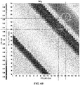
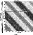
- FIG. 6A is a view illustrating CIE x color coordinate depending on a thickness of a hole auxiliary layer
- FIG. 6B is a view illustrating CIE y color coordinate depending on the thickness of the hole auxiliary layer
- FIG. 6C is a view illustrating current efficiency depending on the thickness of the hole auxiliary layer.
- CIE color coordinates it is referred to Fig. 6D-6F illustrating the CIE color coordinates in 3D colored illustration.
- the thickness of the hole auxiliary layer 182 of the red sub-pixel region Pr is smaller than the thickness of the hole auxiliary layer 182 of the green sub-pixel Pg.
- the hole auxiliary layer 182 of the red sub-pixel region Pr has a thickness corresponding to a second order cavity condition and the hole auxiliary layer 182 of the green sub-pixel region Pg has a thickness corresponding to a third order cavity condition.
- the hole auxiliary layer 182 includes one least one of a hole injecting layer and a hole transporting layer, and a total thickness of the hole injecting layer and the hole transporting layer becomes the thickness of the hole auxiliary layer 182.
- the total thickness of the hole injecting layer and the hole transporting layer in the red sub-pixel region Pr corresponds to the second order cavity condition
- the totoal thickness of the hole injecting layer and the hole transporting layer in the green sub-pixel region Pg corresponds to the third order cavity condition. If the hole auxiliary layer 182 of the red sub-pixel region Pr has a thickness corresponding to a lower order cavity condition than the second order cavity condition, a lifetime of the organic light-emitting diode may be decreased, and if the hole auxiliary layer 182 of the green sub-pixel region Pg has a thickness corresponding to an upper order cavity condition than the third order cavity condition, a driving voltage may be increased.
- the thickness of the hole auxiliary layer 182 of the red sub-pixel region Pr can be 250 nm to 280 nm
- the thickness of the hole auxiliary layer 182 of the green sub-pixel region Pg can be 310 nm to 330 nm.
- the thickness of the hole auxiliary layer 182 of the blue sub-pixel region Pb can be 30 nm to 70 nm.
- the thicknesses of the hole auxiliary layers 182 can be changed by controlling thicknesses of the hole injecting layer HIL and/or the hole transporting layer HTL of the red, green and blue sub-pixel regions Pr, Pg and Pb.
- the thickness of the hole transporting layer HTL is less changed than the thickness of the hole injecting layer HIL.
- the light-emitting material layers 184 of the organic light-emitting diodes De of the red and green sub-pixel regions Pr and Pg include the yellow light-emitting material.
- the yellow light-emitting material has a relatively long lifetime and emits yellowish red light or yellowish green light using the microcavity effect.
- the OLED display device can produce red and green light using the yellow light-emitting material, the microcavity effect and the color filters.
- FIG. 4 is a schematic cross-sectional view showing light outputted from an OLED display device according to the embodiment of the present disclosure.
- FIG. 5A is a view illustrating spectra of light emitted from organic light-emitting diodes of red and green sub-pixel regions of the OLED display device according to the embodiment of the present disclosure
- FIG. 5B is a view illustrating spectra of light outputted from the red and green sub-pixel regions of the OLED display device according to the embodiment of the present disclosure.
- the light-emitting material layers 184 of the red and green sub-pixel regions Pr and Pg include a yellow light-emitting material EML(Y), and the yellow light-emitting material includes first and second emission peaks.
- the yellow light-emitting material can have the first emission peak in a wavelength range of 530 nm to 555 nm and the second emission peak in a wavelength range of 590 nm to 620 nm.
- the yellow light-emitting material can include 4,4'-N,N'-dicarbazole-biphenyl (CBP) and also can include bis[2-(4-tertbutylphenyl)benzothiazolato-N,C2'] iridium(acetylactonate)[(t-bt)2Ir(acac)] as a dopant.
- CBP 4,4'-N,N'-dicarbazole-biphenyl
- the light-emitting material layer 184 including the yellow light-emitting material emits orange light, i.e., yellowish red light Ry due to the microcavity effect.
- the yellowish red light Ry passes through the red color filter Rc, and thus deep red light R (Rp in Fig. 5B ) is outputted.
- the light-emitting material layer 184 including the yellow light-emitting material emits yellowish green light Gy due to the microcavity effect.
- the yellowish green light Gy passes through the green color filter Gc, and thus deep green light G (Gp in Fig. 5B ) is outputted.
- the light-emitting material layer 184 includes a blue light-emitting material and emits blue light B.
- the blue light B passes through the blue color filter Bc, and thus deep blue light B is outputted.
- the OLED display device can produce deep red light and deep green light by applying the yellow light-emitting material, which has a relatively long lifetime, to the red and green sub-pixel regions Pr and Pg and using the microcavity effect and the color filters to thereby produce red and green light. Therefore, the lifetimes of the organic light-emitting diodes of the red and green sub-pixel regions Pr and Pg can be increased.
- a polarizer can be omitted from the OLED display device according to the embodiment of the present disclosure due to the microcavity effects, and thus the costs can be reduced.
- the OLED display device can be a bottom emission type.
Landscapes
- Physics & Mathematics (AREA)
- Optics & Photonics (AREA)
- Engineering & Computer Science (AREA)
- Microelectronics & Electronic Packaging (AREA)
- Electroluminescent Light Sources (AREA)
- Optical Filters (AREA)
- Devices For Indicating Variable Information By Combining Individual Elements (AREA)
Abstract
Description
- The present application claims priority to Korean Patent Application No.
10-2015-0190204 10-2016-0139371 - The present disclosure relates to an organic light-emitting diode display device, and more particularly, to an organic light-emitting diode display device capable of improving a lifetime.
- Recently, flat panel displays have been widely developed and applied to various fields because of their thin profile, light weight, and low power consumption.
- Among the flat panel displays, organic light-emitting diode (OLED) display devices, which can be referred to as organic electroluminescent display devices, emit light during loss of electron-hole pairs. The electron-hole pairs are formed by injecting charges into a light-emitting layer between a cathode for injecting electrons and an anode for injecting holes.
- The OLED display devices can include a flexible substrate such as plastic. Since they are self-luminous, the OLED display devices have excellent contrast ratios. The OLED display devices have a response time of several micro seconds, and there are advantages in displaying moving images. The OLED display devices have wide viewing angles.
- OLED display devices according to driving methods can be passive matrix type OLED display devices and active matrix type OLED display devices. Active matrix type display devices have low power consumption and high definition. In addition, the size of active matrix type display devices can be large.
- An OLED display device includes a plurality of pixels to express various colors. Each pixel includes red, green and blue sub-pixels, and red, green and blue organic light-emitting diodes are formed in the red, green and blue sub-pixels, respectively.
- The red, green and blue organic light-emitting diodes include red, green and blue light-emitting material layers, respectively, and each light-emitting material layer is formed by a thermal evaporation method. More particularly, the light-emitting material layer is formed by selectively vacuum evaporating an organic light-emitting material using a fine metal mask. However, the thermal evaporation method is difficult to be applied to display devices having a large size and high definition due to making deviation, sagging and a shadow effect of the mask.
- To solve this, a method of forming the light-emitting material layer through a solution process has been suggested. In the solution process, a bank layer surrounding a pixel region is formed, a light-emitting material is dropped in the pixel region surrounded by the bank layer by scanning a nozzle of injection apparatus in a certain direction, and the dropped light-emitting material is hardened, there by forming the light-emitting material layer. At this time, a hole injecting layer and a hole transporting layer also may be formed through the solution process.
- By the way, the red, green and blue light-emitting materials have different properties. Specially, the red light-emitting material has relative low efficiency and the green light-emitting material has relatively short lifetime. Thus, it is not easy to secure red, green and blue light-emitting materials having uniform lifetime and efficiency, and a lifetime of the OLED display device is reduced.
- Meanwhile, reflection of the external light is high in the OLED display device. The reflection of the external light increases the brightness at black state, and the contrast ratio is lowered. Therefore, image qualities are decreased because of the reflection of the external light. To prevent the reflection of the external light, at least one polarizer is used, and this causes an increase in costs.
- Accordingly, the present disclosure is directed to an OLED display device that substantially obviates one or more of the problems due to limitations and disadvantages of the related art.
- An object of the present disclosure is to provide an OLED display device that increases a lifetime.
- Another object of the present disclosure is to provide an OLED display device that decreases costs.
- Additional features and advantages of the invention will be set forth in the description which follows, and in part will be apparent from the description, or may be learned by practice of the invention. The objectives and other advantages of the invention will be realized and attained by the structure particularly pointed out in the written description and claims hereof as well as the appended drawings.
- The objects are solved by the features of the independent claims. Preferred embodiments are given in the dependent claims.
- To achieve these and other advantages and in accordance with the purpose of the present invention, as embodied and broadly described herein, there is provided an organic light-emitting diode display device includes a substrate on which red, green and blue sub-pixel regions are defined; first electrodes in the red, green and blue sub-pixel regions, respectively; first, second and third light-emitting layers on the corresponding first electrodes and in the red, green and blue sub-pixel regions, respectively; a second electrode on the first, second and third light-emitting layers; and red, green and blue color filters on the second electrode and corresponding to the red, green and blue sub-pixel regions, respectively, wherein a thickness of the first light-emitting layer is smaller than a thickness of the second light emitting layer.
- In an other embodiment an organic light-emitting diode display device is provided comprising: a substrate on which red, green and blue sub-pixel regions are defined; a first electrode in each of the red, green and blue sub-pixel regions; first, second and third light-emitting layers on the first electrodes in the red, green and blue sub-pixel regions, respectively, each of the first and second light-emitting layers including a yellow light-emitting material having a first emission peak and a second emission peak different from the first emission peak; a second electrode on the first, second and third light-emitting layers; and red, green and blue color filters on the second electrode and corresponding to the red, green and blue sub-pixel regions, respectively.
- Preferably, a thickness of the first light-emitting layer is smaller than a thickness of the second light emitting layer.
- In another embodiment an organic light-emitting diode display device is provided, wherein each of the first and second light-emitting layers including a yellow light-emitting material having a first emission peak and a second emission peak different from the first emission peak and the thickness of the first light-emitting layer is smaller than a thickness of the second light emitting layer.
- Preferably, the third light-emitting layer includes a blue light-emitting material.
- Preferably, a thickness of the third light-emitting layer is smaller than the thickness of the first light-emitting layer
- Preferably, each of the first and second light-emitting layers includes a yellow light-emitting material.
- Preferably, the yellow light-emitting material has a first emission peak within a wavelength range of 530 nm to 555 nm and a second emission peak within a wavelength range of 590 nm to 620 nm.
- Preferably, the yellow light-emitting material includes 4,4'-N,N'-dicarbazole-biphenyl (CBP) and also includes bis[2-(4-tertbutylphenyl)benzothiazolato-N,C2']iridium(acetylactonate)[(t-bt)2Ir(acac)] as a dopant.
- Preferably, each of the first and second light-emitting layers include a hole auxiliary layer, a light-emitting material layer and an electron auxiliary layer, and wherein a thickness of the hole auxiliary layer of the first light-emitting layer is smaller than a thickness of the hole auxiliary layer of the second light-emitting layer.
- Preferably, the thickness of the hole auxiliary layer of the first light-emitting layer corresponds to a second order cavity condition, and the thickness of the hole auxiliary layer of the second light-emitting layer corresponds to a third order cavity condition.
- Preferably, the thickness of the hole auxiliary layer of the first light-emitting layer is 250 nm to 280 nm, and the thickness of the hole auxiliary layer of the second light-emitting layer is 310 nm to 330 nm.
- Preferably, each of the first and the third light-emitting layer includes a hole auxiliary layer, a light-emitting material layer and an electron auxiliary layer, and wherein a thickness of the hole auxiliary layer of the third light-emitting layer is smaller than a thickness of the hole auxiliary layer of the first light-emitting layer.
- Preferably, the thickness of the hole auxiliary layer of the third light-emitting layer is 30 nm to 70 nm.
- Preferably, each of the first and the third light-emitting layer includes a hole auxiliary layer, a light-emitting material layer and an electron auxiliary layer, and wherein a thickness of the hole auxiliary layer of the third light-emitting layer is smaller than a thickness of the hole auxiliary layer of the first light-emitting layer.
- Preferably, the thickness of the hole auxiliary layer of the third light-emitting layer is 30 nm to 70 nm.
- Preferably, a bank layer of an insulating material is disposed on the first electrode, the bank layer has an opening exposing the first electrode, and covers edges of the first electrode, each of the first, second and third light-emitting layers is formed on the first electrode exposed by the opening of the bank layer.
- Preferably, the bank layer has a single-layered structure or a double-layered structure.
- Preferably, the bank layer includes a first bank and a second bank on the first bank, and the first bank has a wider width than the second bank.
- Preferably, the first bank is formed of an inorganic insulating material or organic insulating material having a hydrophilic property, and the second bank is formed of an organic insulating material having a hydrophobic property.
- It is to be understood that both the foregoing general description and the following detailed description are exemplary and explanatory and are intended to provide further explanation of the invention as claimed.
- The accompanying drawings, which are included to provide a further understanding of the invention and are incorporated in and constitute a part of this specification, illustrate embodiments of the invention and together with the description serve to explain the principles of the invention. In the drawings:
-
FIG. 1 is a circuit diagram of one pixel region of an OLED display device according to an embodiment of the present disclosure; -
FIG. 2 is a cross-sectional view of an OLED display device according to the embodiment of the present disclosure ; -
FIG. 3 is a schematic view of red, green and blue sub-pixels of an OLED display device according to the embodiment of the present disclosure; -
FIG. 4 is a schematic cross-sectional view showing light outputted from an OLED display device according to the embodiment of the present disclosure; and -
FIG. 5A is a view illustrating spectra of light emitted from organic light-emitting diodes of red and green sub-pixel regions of the OLED display device according to the embodiment of the present disclosure, andFIG. 5B is a view illustrating spectra of light outputted from the red and green sub-pixel regions of the OLED display device according to the embodiment of the present disclosure. -
FIG. 6A is a view illustrating CIE x color coordinate depending on a thickness of a hole auxiliary layer,FIG. 6B is a view illustrating CIE y color coordinate depending on the thickness of the hole auxiliary layer, andFIG. 6C is a view illustrating current efficiency depending on the thickness of the hole auxiliary layer, whereasFig. 6A-6C illustrate the CIE color coordinates in 2D colored illustration; -
FIG. 6D is a view illustrating CIE x color coordinate depending on a thickness of a hole auxiliary layer,FIG. 6E is a view illustrating CIE y color coordinate depending on the thickness of the hole auxiliary layer, andFIG. 6F is a view illustrating current efficiency depending on the thickness of the hole auxiliary layer, whereasFig. 6D-6F illustrate the CIE color coordinates in 3D colored illustration. - Reference will now be made in detail to the embodiment of the disclosure, an example of which is illustrated in the accompanying drawings. Words of 'on' and 'under' are used only for describing a direction in the following explanations and thus are not limited to 'directly on' and 'directly under'.
-
FIG. 1 is a circuit diagram of one pixel region of an OLED display device according to an embodiment of the present disclosure. - As shown in
FIG. 1 , the OLED display device according to the embodiment of the present disclosure includes a gate line GL, a data line DL, a switching thin film transistor Ts, a driving thin film transistor Td, a storage capacitor Cst and an organic light-emitting diode De. The gate line GL and the data line DL cross each other to define a pixel region P. The switching thin film transistor Ts, the driving thin film transistor Td, the storage capacitor Cst and the organic light-emitting diode De are formed in the pixel region P. - More particularly, a gate electrode of the switching thin film transistor Ts is connected to the gate line GL, and a source electrode of the switching thin film transistor Ts is connected to the data line DL. A gate electrode of the driving thin film transistor Td is connected to a drain electrode of the switching thin film transistor Ts, and a source electrode of the driving thin film transistor Td is connected to a high voltage supply VDD. An anode of the organic light-emitting diode De is connected to a drain electrode of the driving thin film transistor Td, and a cathode of the organic light-emitting diode De is connected to a low voltage supply VSS. The storage capacitor Cst is connected to the gate electrode and the drain electrode of the driving thin film transistor Td.
- The OLED display device is driven to display an image. More particularly, when the switching thin film transistor Ts is turned on by a gate signal applied through the gate line GL, a data signal from the data line DL is applied to the gate electrode of the driving thin film transistor Td and an electrode of the storage capacitor Cst through the switching thin film transistor Ts. When the driving thin film transistor Td is turned on by the data signal, an electric current flowing through the organic light-emitting diode De is controlled, thereby displaying an image. The organic light-emitting diode De emits light due to the current supplied through the driving thin film transistor Td from the high voltage supply VDD.
- Namely, the amount of the current flowing through the organic light-emitting diode De is proportional to the magnitude of the data signal, and the intensity of light emitted by the organic light-emitting diode De is proportional to the amount of the current flowing through the organic light-emitting diode De. Thus, the pixel regions P show different gray levels depending on the magnitude of the data signal, and as a result, the OLED display device displays an image.
- The storage capacitor Cst maintains charges corresponding to the data signal for a frame when the switching thin film transistor Ts is turned off. Accordingly, even if the switching thin film transistor Ts is turned off, the storage capacitor Cst allows the amount of the current flowing through the organic light-emitting diode De to be constant and the gray level shown by the organic light-emitting diode De to be maintained until a next frame.
- However, the OLED display device according to the embodiment of the present disclosure is not limited to the illustrated example. Alternatively, at least one thin film transistor, at least one signal line and/or at least one capacitor for compensation may be further formed in each pixel region.
-
FIG. 2 is a cross-sectional view of an OLED display device according to the embodiment of the present disclosure and shows a pixel region. - In
FIG. 2 , asemiconductor layer 122 is patterned and formed on an insulatingsubstrate 110. Thesubstrate 110 can be a glass substrate or a plastic substrate. Thesemiconductor layer 122 can be formed of an oxide semiconductor material. In the OLED display device including thesemiconductor layer 122 formed of an oxide semiconductor material, a light-blocking pattern (not shown) and a buffer layer (not shown) are formed under thesemiconductor layer 122. The light-blocking pattern blocks light from the outside or light emitted from a light-emitting diode to prevent thesemiconductor layer 122 from being degraded by the light. Alternatively, thesemiconductor layer 122 can be formed of poly crystalline silicon, and in this case, impurities can be doped in both sides of thesemiconductor layer 122. - A
gate insulating layer 130 of an insulating material is formed on thesemiconductor layer 122 over substantially all of thesubstrate 110. Thegate insulating layer 130 can be formed of an inorganic insulating material such as silicon oxide (SiO2). When thesemiconductor layer 122 is formed of polycrystalline silicon, thegate insulating layer 130 can be formed of silicon oxide (SiO2) or silicon nitride (SiNx). - A
gate electrode 132 of a conductive material such as metal can be formed on thegate insulating layer 130 to correspond to thesemiconductor layer 122. In addition, a gate line (not shown) and a first capacitor electrode (not shown) can be formed on thegate insulating layer 130. The gate line extends in a first direction, and the first capacitor electrode can be connected to thegate electrode 132. - The OLED display device according to the embodiment of the present disclosure includes the
gate insulating layer 130 formed over substantially all of thesubstrate 110. Alternatively, thegate insulating layer 130 can be patterned to have the same shape as thegate electrode 132. - An
inter insulating layer 140 of an insulating material is formed on thegate electrode 132 over substantially all of thesubstrate 110. Theinter insulating layer 140 can be formed of an inorganic insulating material such as silicon oxide (SiO2) and silicon nitride (SiNx) or an organic insulating material such as benzocyclobutene and photo acryl. - The
inter insulating layer 140 includes first andsecond contact holes semiconductor layer 122. The first andsecond contact holes gate electrode 132, and thegate electrode 132 is disposed between the first andsecond contact holes second contact holes gate insulating layer 130. Alternatively, when thegate insulating layer 130 is patterned to have the same shape as thegate electrode 132, the first andsecond contact holes inter insulating layer 140. - A
source electrode 142 and adrain electrode 144 of a conductive material such as metal are formed on theinter insulating layer 140. In addition, a data line (not shown), a power supply line (not shown) and a second capacitor electrode (not shown) can be formed on theinter insulating layer 140. The data line and the power supply line extend in a second direction. - The source and drain
electrodes gate electrode 132. The source and drainelectrodes semiconductor layer 122 through the first andsecond contact holes drain electrode 144 and can overlap the first capacitor electrode to form a storage capacitor with theinter insulating layer 140 therebetween as a dielectric substance. - In the OLED display device, a thin film transistor includes the
semiconductor layer 122, thegate electrode 132, thesource electrode 142 and thedrain electrode 144. The thin film transistor can have a coplanar structure where thegate electrode 132 and the source and drainelectrodes semiconductor layer 122, i.e., over thesemiconductor layer 122. - Alternatively, the thin film transistor can have an inverted staggered structure where the gate electrode is disposed under the semiconductor layer and the source and drain electrodes are disposed over the semiconductor layer. In this case, the semiconductor layer can be formed of amorphous silicon.
- In addition, the thin film transistor can be a driving thin film transistor of the OLED display device. A switching thin film transistor can have the same structure as the driving thin film transistor formed over the
substrate 110. At this time, thegate electrode 132 of the driving thin film transistor is connected to a drain electrode of the switching thin film transistor, and thesource electrode 142 of the driving thin film transistor is connected to the power supply line. In addition, the gate electrode and the source electrode of the switching thin film transistor are connected to the gate line and the data line, respectively. - A
first passivation layer 152 and asecond passivation layer 154 of insulating materials are sequentially formed on the source and drainelectrodes substrate 110. Thefirst passivation layer 152 can be formed of an inorganic insulating material such as silicon oxide (SiO2) and silicon nitride (SiNx), and thesecond passivation layer 154 can be formed of an organic insulating material such as benzocyclobutene and photo acryl. Thesecond passivation layer 154 can have a flat top surface. - The
first passivation layer 152 and thesecond passivation layer 154 have adrain contact hole 156 exposing thedrain electrode 144. InFig. 2 , although thedrain contact hole 156 is formed directly over thesecond contact hole 140b, thedrain contact hole 156 can be spaced apart from thesecond contact hole 140b. - One of the
first passivation layer 152 and thesecond passivation layer 154 can be omitted. For example, thefirst passivation layer 152 of an inorganic insulating material can be omitted. - A
first electrode 162 of a conductive material having a relatively high work function is formed on thesecond passivation layer 154. Thefirst electrode 162 is disposed in each pixel region and contacts thedrain electrode 144 through thedrain contact hole 156. For example, thefirst electrode 162 can be formed of a transparent conductive material such as indium tin oxide (ITO) and indium zinc oxide (IZO). - A
bank layer 170 of an insulating material is formed on thefirst electrode 162. Thebank layer 170 is disposed between adjacent pixel regions, has an opening exposing thefirst electrode 162, and covers edges of thefirst electrode 162. - In the OLED display device, the
bank layer 170 has a single-layered structure, and the structure of thebank layer 170 is not limited to this. For example, the bank layer can have a double-layered structure. That is, the bank layer can include a first bank and a second bank on the first bank, and the first bank can have a wider width than the second bank. At this time, the first bank can be formed of an inorganic insulating material or organic insulating material having a hydrophilic property, and the second bank can be formed of an organic insulating material having a hydrophobic property. - A light-emitting
layer 180 is formed on thefirst electrode 162 exposed by the opening of thebank layer 170. The light-emittinglayer 180 includes a holeauxiliary layer 182, a light-emitting material layer (EML) 184, and anelectron auxiliary layer 186, which are sequentially disposed from a top surface of thefirst electrode 162. - The hole
auxiliary layer 182, the light-emittingmaterial layer 184 and theelectron auxiliary layer 186 can be formed of organic materials and can be formed through a solution process, which may be referred to as a soluble process. Accordingly, manufacturing processes can be simplified, and a display device having a large size and high definition can be provided. One of a spin coating method, an inkjet printing method and a screen printing method can be used for the solution process. - Alternatively, the hole
auxiliary layer 182, the light-emittingmaterial layer 184 and theelectron auxiliary layer 186 can be formed through a vacuum evaporation process. In addition, the holeauxiliary layer 182, the light-emittingmaterial layer 184 and theelectron auxiliary layer 186 can be formed by a combination of the solution process and the vacuum evaporation process. - The hole
auxiliary layer 182 can include at least one of a hole injecting layer (HIL) and a hole transporting layer (HTL), and theelectron auxiliary layer 186 can include at least one of an electron injecting layer (EIL) and an electron transporting layer (ETL). - A
second electrode 192 of a conductive material having relatively low work function is formed on theelectron auxiliary layer 186 over substantially all of thesubstrate 110. Here, thesecond electrode 192 can be formed of aluminum (Al), magnesium (Mg), silver (Ag) or their alloy. - The
first electrode 162, the light-emittinglayer 180 and thesecond electrode 192 constitute an organic light-emitting diode De. Thefirst electrode 162 functions as an anode, and thesecond electrode 192 serves as a cathode. Here, the OLED display device according to the embodiment of the present disclosure is an active matrix type and is a top emission type in which light from the light-emittingmaterial layer 184 is outputted to the outside through thesecond electrode 192. In this case, thefirst electrode 162 can further include a reflection layer (not shown) formed of an opaque conductive material. For example, the reflection layer can be formed of aluminum-paladium-copper (APC) alloy, and thefirst electrode 162 can have a triple-layered structure of ITO/APC/ITO. In addition, thesecond electrode 192 can have a relatively thin thickness such that light is transmitted therethrough. For example, thesecond electrode 192 can have transmittance of about 45% to 50%. - The OLED display device according to the embodiment of the present disclosure includes a plurality of pixels, and each pixel includes red, green and blue sub-pixels. The thin film transistor and the organic light-emitting diode of
FIG. 2 are formed in each red, green and blue sub-pixel region. - At this time, the organic light-emitting diodes of the red, green and blue sub-pixels have different element thicknesses. This will be described in more detail with reference to accompanying drawings.
-
FIG. 3 is a schematic view of red, green and blue sub-pixels of an OLED display device according to the embodiment of the present disclosure. - In
FIG. 3 , red, green and blue sub-pixel regions Pr, Pg and Pb are defined on asubstrate 110, and an organic light-emitting diode De is disposed in each sub-pixel region Pr, Pg and Pb. The organic light-emitting diode De in each sub-pixel region Pr, Pg and Pb includes afirst electrode 162, a light-emittinglayer 180 and asecond electrode 192. - The
first electrode 162 can be an anode and can be formed of a conductive material having relatively high work function. Thefirst electrode 162 can include a transparent conductive material such as indium tin oxide (ITO) and indium zinc oxide (IZO). In addition, thefirst electrode 162 can further include a reflection layer at its lowest portion. - Even if the
first electrodes 162 are connected to each other in the red, green and blue sub-pixel regions Pr, Pg and Pb, thefirst electrodes 162 are distinguished from each other by the red, green and blue sub-pixel regions Pr, Pg and Pb. - The light-emitting
layer 180 is disposed on thefirst electrode 162 in each sub-pixel region Pr, Pg and Pb. The light-emittinglayer 180 includes a holeauxiliary layer 182, a light-emittingmaterial layer 184 and anelectron auxiliary layer 186. - Here, the light-emitting material layers 184 of the red and green sub-pixel regions Pr and Pg include a yellow light-emitting material EML(Y), and the light-emitting
material layer 184 of the blue sub-pixel region Pb includes a blue light-emitting material EML(B). - The light-emitting material layers 184 can be formed through a solution process. Alternatively, the light-emitting material layers 184 can be formed through a solution process and a vacuum evaporation process. Namely, the light-emitting material layers 184 of the red and green sub-pixel regions Pr and Pg can be formed through the solution process, and the light-emitting
material layer 184 of the blue sub-pixel region Pb can be formed through the vacuum evaporation process. - Moreover, the hole
auxiliary layer 182 can include a hole injecting layer (HIL) and a hole transporting layer (HTL). At this time, the holeauxiliary layers 182 of the red, green and blue sub-pixel regions Pr, Pg and Pb can have different thicknesses. More particularly, the thickness of the holeauxiliary layer 182 of the red sub-pixel region Pr is smaller than the thickness of the holeauxiliary layer 182 of the green sub-pixel region Pg and is larger than the thickness of the holeauxiliary layer 182 of the blue sub-pixel region Pb. - The hole
auxiliary layers 182 can be formed through the solution process, and the thicknesses of the holeauxiliary layers 182 can be adjusted by changing the amount of dropped solution. - In the meantime, the
electron auxiliary layer 186 can include an electron transporting layer (ETL). Theelectron auxiliary layer 186 can further include an electron injecting layer on the electron transporting layer ETL. Theelectron auxiliary layer 186 can be formed through the vacuum evaporation process. - The
second electrode 192 as a cathode is disposed on the light-emittinglayers 180 of the red, green and blue sub-pixel regions Pr, Pg and Pb. Thesecond electrode 192 can be formed of aluminum (Al), magnesium (Mg), silver (Ag) or their alloy. Thesecond electrode 192 can have a relatively thin thickness such that light can be transmitted therethrough. - An
encapsulation layer 200 is formed on the organic light-emitting diode De to protect the organic light-emitting diode De from moisture and oxygen from the outside. Theencapsulation layer 200 can be formed of ultraviolet (UV) sealant or frit sealant. Alternatively, theencapsulation layer 200 can be formed of inorganic layers and organic layers, which are alternately disposed. - A
color filter layer 220 is disposed on theencapsulation layer 200. Thecolor filter layer 220 can include red, green and blue color filters Rc, Gc and Bc corresponding to the red, green and blue sub-pixel regions Pr, Pg and Pb. Here, the blue color filter Bc can be omitted. - An overcoat layer (not shown) can be further formed between the
encapsulation layer 200 and thecolor filter layer 220 to protect thecolor filter layer 200 and flatten a top surface. - An
opposite substrate 210 is disposed on thecolor filter layer 220. Theopposite substrate 210 can be a glass substrate or a plastic substrate. - Here, the
color filter layer 220 can be formed on theopposite substrate 210, and theopposite substrate 210 including thecolor filter layer 220 thereon can be attached to thesubstrate 110 including the organic light-emitting diode De. - The OLED display device according to the embodiment of the present disclosure can be a top emission type where light from the light-emitting
layer 180 is outputted to the outside through thesecond electrode 192. - As stated above, in the OLED display device according to the embodiment of the present disclosure, the organic light-emitting diodes De of the red, green and blue sub-pixel regions Pr, Pg and Pb have different element thicknesses. That is, when each of the organic light-emitting diodes De of the red, green and blue sub-pixel regions Pr, Pg and Pb has a distance from a bottom surface of the
first electrode 162 and a top surface of thesecond electrode 192 as an element thickness, the element thickness of the organic light-emitting diode De of the red sub-pixel region Pr is smaller than the element thickness of the organic light-emitting diode De of the green sub-pixel region Pg and is larger than the element thickness of the organic light-emitting diode De of the blue sub-pixel region Pb. - At this time, the element thicknesses of the organic light-emitting diodes De of the red, green and blue sub-pixel regions Pr, Pg and Pb can be different from each other by differing thicknesses of the light-emitting
layers 180, and more particularly, thicknesses of the hole auxiliary layers 182. Namely, the holeauxiliary layer 182 of the red sub-pixel region Pr is formed to have the thickness smaller than the thickness of the holeauxiliary layer 182 of the green sub-pixel region Pg and larger than the thickness of the holeauxiliary layer 182 of the blue sub-pixel region Pb. - The thicknesses of the hole
auxiliary layers 182 can be determined by considering a microcavity effect. -
FIG. 6A is a view illustrating CIE x color coordinate depending on a thickness of a hole auxiliary layer,FIG. 6B is a view illustrating CIE y color coordinate depending on the thickness of the hole auxiliary layer, andFIG. 6C is a view illustrating current efficiency depending on the thickness of the hole auxiliary layer. For further illustrating the CIE color coordinates it is referred toFig. 6D-6F illustrating the CIE color coordinates in 3D colored illustration. - In
FIGs. 6A to 6F , to obtain relatively high current efficiency and satisfy required color coordinates, it is desirable that the thickness of the holeauxiliary layer 182 of the red sub-pixel region Pr is smaller than the thickness of the holeauxiliary layer 182 of the green sub-pixel Pg. Especially, it is beneficial that the holeauxiliary layer 182 of the red sub-pixel region Pr has a thickness corresponding to a second order cavity condition and the holeauxiliary layer 182 of the green sub-pixel region Pg has a thickness corresponding to a third order cavity condition. As stated above, the holeauxiliary layer 182 includes one least one of a hole injecting layer and a hole transporting layer, and a total thickness of the hole injecting layer and the hole transporting layer becomes the thickness of the holeauxiliary layer 182. Thus, the total thickness of the hole injecting layer and the hole transporting layer in the red sub-pixel region Pr corresponds to the second order cavity condition, and the totoal thickness of the hole injecting layer and the hole transporting layer in the green sub-pixel region Pg corresponds to the third order cavity condition. If the holeauxiliary layer 182 of the red sub-pixel region Pr has a thickness corresponding to a lower order cavity condition than the second order cavity condition, a lifetime of the organic light-emitting diode may be decreased, and if the holeauxiliary layer 182 of the green sub-pixel region Pg has a thickness corresponding to an upper order cavity condition than the third order cavity condition, a driving voltage may be increased. For example, the thickness of the holeauxiliary layer 182 of the red sub-pixel region Pr can be 250 nm to 280 nm, the thickness of the holeauxiliary layer 182 of the green sub-pixel region Pg can be 310 nm to 330 nm. At this time, if the thickness of the holeauxiliary layer 182 in each of the red and green sub-pixel regions Pr and Pg is not within the above-mentioned range, yellow light is mixed and emitted in each of the red and green sub-pixel regions Pr and Pg, and the color coordinates are not matched. - Meanwhile, the thickness of the hole
auxiliary layer 182 of the blue sub-pixel region Pb can be 30 nm to 70 nm. - At this time, the thicknesses of the hole
auxiliary layers 182 can be changed by controlling thicknesses of the hole injecting layer HIL and/or the hole transporting layer HTL of the red, green and blue sub-pixel regions Pr, Pg and Pb. In general, since carrier mobility of the hole transporting layer HTL is larger than that of the hole injecting layer HIL, it is beneficial that the thickness of the hole transporting layer HTL is less changed than the thickness of the hole injecting layer HIL. - Meanwhile, as mentioned above, the light-emitting material layers 184 of the organic light-emitting diodes De of the red and green sub-pixel regions Pr and Pg include the yellow light-emitting material. The yellow light-emitting material has a relatively long lifetime and emits yellowish red light or yellowish green light using the microcavity effect.
- Accordingly, the OLED display device according to the embodiment of the present disclosure can produce red and green light using the yellow light-emitting material, the microcavity effect and the color filters.
-
FIG. 4 is a schematic cross-sectional view showing light outputted from an OLED display device according to the embodiment of the present disclosure.FIG. 5A is a view illustrating spectra of light emitted from organic light-emitting diodes of red and green sub-pixel regions of the OLED display device according to the embodiment of the present disclosure, andFIG. 5B is a view illustrating spectra of light outputted from the red and green sub-pixel regions of the OLED display device according to the embodiment of the present disclosure. - In
FIG. 4 ,FIG. 5A and FIG. 5B , the light-emitting material layers 184 of the red and green sub-pixel regions Pr and Pg include a yellow light-emitting material EML(Y), and the yellow light-emitting material includes first and second emission peaks. At this time, the yellow light-emitting material can have the first emission peak in a wavelength range of 530 nm to 555 nm and the second emission peak in a wavelength range of 590 nm to 620 nm. For example, the yellow light-emitting material can include 4,4'-N,N'-dicarbazole-biphenyl (CBP) and also can include bis[2-(4-tertbutylphenyl)benzothiazolato-N,C2'] iridium(acetylactonate)[(t-bt)2Ir(acac)] as a dopant. - Here, in the red sub-pixel region Pr, the light-emitting
material layer 184 including the yellow light-emitting material emits orange light, i.e., yellowish red light Ry due to the microcavity effect. The yellowish red light Ry passes through the red color filter Rc, and thus deep red light R (Rp inFig. 5B ) is outputted. - Additionally, in the green sub-pixel region Pg, the light-emitting
material layer 184 including the yellow light-emitting material emits yellowish green light Gy due to the microcavity effect. The yellowish green light Gy passes through the green color filter Gc, and thus deep green light G (Gp inFig. 5B ) is outputted. - Meanwhile, in the blue sub-pixel region Pb, the light-emitting
material layer 184 includes a blue light-emitting material and emits blue light B. The blue light B passes through the blue color filter Bc, and thus deep blue light B is outputted. - Like this, the OLED display device according to the present disclosure can produce deep red light and deep green light by applying the yellow light-emitting material, which has a relatively long lifetime, to the red and green sub-pixel regions Pr and Pg and using the microcavity effect and the color filters to thereby produce red and green light. Therefore, the lifetimes of the organic light-emitting diodes of the red and green sub-pixel regions Pr and Pg can be increased.
- Moreover, a polarizer can be omitted from the OLED display device according to the embodiment of the present disclosure due to the microcavity effects, and thus the costs can be reduced.
- Even if the OLED display device is the top emission type in the above-mentioned embodiment, the OLED display device can be a bottom emission type.
- It will be apparent to those skilled in the art that various modifications and variations can be made in a display device of the present disclosure without departing from the scope of the invention. Thus, it is intended that the present invention covers the modifications and variations of this invention provided they come within the scope of the appended claims and their equivalents.
Claims (15)
- An organic light-emitting diode display device comprising:a substrate (110) on which red, green and blue sub-pixel regions (Pr, Pg, Pb) are defined;first electrodes (162) in the red, green and blue sub-pixel regions (Pr, Pg, Pb), respectively;first, second and third light-emitting layers (180) on the corresponding first electrodes (162) and in the red, green and blue sub-pixel regions (Pr, Pg, Pb), respectively;a second electrode (192) on the first, second and third light-emitting layers (180); andred, green and blue color filters (220) on the second electrode (192) and corresponding to the red, green and blue sub-pixel regions (Pr, Pg, Pb), respectively,wherein a thickness of the first light-emitting layer is smaller than a thickness of the second light emitting layer; and/orwherein each of the first and second light-emitting layers including a yellow light-emitting material (EML(Y)) having a first emission peak and a second emission peak different from the first emission peak.
- The organic light-emitting diode display device of claim 1, wherein the third light-emitting layer includes a blue light-emitting material (EML(B)).
- The organic light-emitting diode display device of claim 1 or 2, wherein a thickness of the third light-emitting layer (180) is smaller than the thickness of the first light-emitting layer
- The organic light-emitting diode display device as claimed in any one of the preceding claims, wherein the yellow light-emitting material has a first emission peak within a wavelength range of 530 nm to 555 nm and a second emission peak within a wavelength range of 590 nm to 620 nm.
- The organic light-emitting diode display device as claimed in any one of the preceding claims, wherein the yellow light-emitting material includes 4,4'-N,N'-dicarbazole-biphenyl (CBP) and also includes bis[2-(4-tertbutylphenyl)benzothiazolato-N,C2']iridium(acetylactonate)[(t-bt)2Ir(acac)] as a dopant.
- The organic light-emitting diode display device as claimed in any one of the preceding claims, wherein each of the first and second light-emitting layers include a hole auxiliary layer (182), a light-emitting material layer (184) and an electron auxiliary layer (186), and wherein a thickness of the hole auxiliary layer (182) of the first light-emitting layer is smaller than a thickness of the hole auxiliary layer (182) of the second light-emitting layer.
- The organic light-emitting diode display device of claim 6, wherein the thickness of the hole auxiliary layer (182) of the first light-emitting layer corresponds to a second order cavity condition, and the thickness of the hole auxiliary layer (182) of the second light-emitting layer corresponds to a third order cavity condition.
- The organic light-emitting diode display device of claim 6 or 7, wherein the thickness of the hole auxiliary layer (182) of the first light-emitting layer is 250 nm to 280 nm, and the thickness of the hole auxiliary layer (182) of the second light-emitting layer is 310 nm to 330 nm.
- The organic light-emitting diode display device as claimed in any one of the preceding claims, wherein each of the first and the third light-emitting layer (180) includes a hole auxiliary layer (182), a light-emitting material layer (184) and an electron auxiliary layer (186), and wherein a thickness of the hole auxiliary layer (182) of the third light-emitting layer is smaller than a thickness of the hole auxiliary layer of the first light-emitting layer (182).
- The organic light-emitting diode display device as claimed in any one of the preceding claims 6-9, wherein each of the first and the third light-emitting layer (180) includes a hole auxiliary layer (182), a light-emitting material layer (184) and an electron auxiliary layer (186), and wherein a thickness of the hole auxiliary layer (182) of the third light-emitting layer (180) is smaller than a thickness of the hole auxiliary layer (182) of the first light-emitting layer (180).
- The organic light-emitting diode display device as claimed in any one of the preceding claims 6-10, wherein the thickness of the hole auxiliary layer (182) of the third light-emitting layer (180) is 30 nm to 70 nm.
- The organic light-emitting diode display device as claimed in any one of the preceding claims, wherein a bank layer (170) of an insulating material is disposed on the first electrode (162), the bank layer (170) has an opening exposing the first electrode (162), and covers edges of the first electrode (162), each of the first, second and third light-emitting layers (180) is formed on the first electrode (162) exposed by the opening of the bank layer (170).
- The organic light-emitting diode display device of claim 12, wherein the bank layer (170) has a single-layered structure or a double-layered structure.
- The organic light-emitting diode display device of claim 12 or 13, wherein the bank layer (170) includes a first bank and a second bank on the first bank, and the first bank has a wider width than the second bank.
- The organic light-emitting diode display device of claim 14, wherein the first bank is formed of an inorganic insulating material or organic insulating material having a hydrophilic property, and the second bank is formed of an organic insulating material having a hydrophobic property.
Applications Claiming Priority (2)
| Application Number | Priority Date | Filing Date | Title |
|---|---|---|---|
| KR20150190204 | 2015-12-30 | ||
| KR1020160139371A KR102690328B1 (en) | 2015-12-30 | 2016-10-25 | Organic Light Emitting Diode Display Device |
Publications (2)
| Publication Number | Publication Date |
|---|---|
| EP3188276A1 true EP3188276A1 (en) | 2017-07-05 |
| EP3188276B1 EP3188276B1 (en) | 2020-11-25 |
Family
ID=57737611
Family Applications (1)
| Application Number | Title | Priority Date | Filing Date |
|---|---|---|---|
| EP16207237.5A Active EP3188276B1 (en) | 2015-12-30 | 2016-12-29 | Organic light-emitting diode display device |
Country Status (3)
| Country | Link |
|---|---|
| US (1) | US10170521B2 (en) |
| EP (1) | EP3188276B1 (en) |
| JP (1) | JP6514679B2 (en) |
Cited By (1)
| Publication number | Priority date | Publication date | Assignee | Title |
|---|---|---|---|---|
| CN111223891A (en) * | 2018-11-26 | 2020-06-02 | 乐金显示有限公司 | Display device |
Families Citing this family (15)
| Publication number | Priority date | Publication date | Assignee | Title |
|---|---|---|---|---|
| JP6816102B2 (en) * | 2016-03-01 | 2021-01-20 | パイオニア株式会社 | Manufacturing method of light emitting device |
| CN108886856B (en) * | 2016-03-29 | 2020-04-10 | 夏普株式会社 | Organic EL display device and method for manufacturing organic EL display device |
| CN106960862B (en) * | 2017-03-15 | 2019-10-25 | 合肥鑫晟光电科技有限公司 | A display substrate and a display device |
| CN109119438B (en) * | 2017-06-26 | 2020-11-24 | 京东方科技集团股份有限公司 | Display substrate, method for manufacturing the same, and display device |
| CN109428005B (en) | 2017-08-30 | 2020-05-08 | 昆山国显光电有限公司 | Organic electroluminescent device |
| CN107591432B (en) * | 2017-09-27 | 2020-05-26 | 京东方科技集团股份有限公司 | Pixel defining layer, display substrate, manufacturing method and display device |
| KR102480330B1 (en) * | 2017-12-27 | 2022-12-21 | 엘지디스플레이 주식회사 | Organic light emitting diodes display |
| US11362306B2 (en) * | 2018-03-06 | 2022-06-14 | Sony Semiconductor Solutions Corporation | Light emitting element unit |
| KR102643070B1 (en) * | 2018-12-07 | 2024-02-29 | 엘지디스플레이 주식회사 | Electroluminescent Display Device |
| KR102819422B1 (en) * | 2019-12-27 | 2025-06-11 | 엘지디스플레이 주식회사 | Electroluminescent Display Device |
| CN111312798A (en) * | 2020-04-09 | 2020-06-19 | 武汉华星光电半导体显示技术有限公司 | Flexible display panel and manufacturing method thereof |
| US11980046B2 (en) * | 2020-05-27 | 2024-05-07 | Taiwan Semiconductor Manufacturing Company, Ltd. | Method for forming an isolation structure having multiple thicknesses to mitigate damage to a display device |
| KR20230085741A (en) * | 2021-12-07 | 2023-06-14 | 엘지디스플레이 주식회사 | Display apparatus |
| KR20230103436A (en) * | 2021-12-31 | 2023-07-07 | 엘지디스플레이 주식회사 | Organic light emitting display device and method for manufacturing the same |
| CN114447094B (en) * | 2022-04-11 | 2022-09-02 | 北京京东方技术开发有限公司 | Display substrate and display device |
Citations (4)
| Publication number | Priority date | Publication date | Assignee | Title |
|---|---|---|---|---|
| US20100156279A1 (en) * | 2008-12-19 | 2010-06-24 | Shinichiro Tamura | Organic emitting device |
| US20100156280A1 (en) * | 2008-12-19 | 2010-06-24 | Samsung Electronics Co., Ltd. | Organic light emitting device and method for manufacturing the same |
| US20140110682A1 (en) * | 2012-10-22 | 2014-04-24 | Au Optronics Corp. | Pixel structure of electroluminescent display panel |
| US20140139102A1 (en) * | 2012-11-20 | 2014-05-22 | Lg Display Co., Ltd. | Organic light emitting diode display device and method of fabricating the same |
Family Cites Families (56)
| Publication number | Priority date | Publication date | Assignee | Title |
|---|---|---|---|---|
| US7030553B2 (en) * | 2003-08-19 | 2006-04-18 | Eastman Kodak Company | OLED device having microcavity gamut subpixels and a within gamut subpixel |
| EP2509397B1 (en) * | 2003-09-19 | 2018-12-05 | Sony Corporation | Display unit with resonator structure |
| JP4428979B2 (en) * | 2003-09-30 | 2010-03-10 | 三洋電機株式会社 | Organic EL panel |
| JP4716699B2 (en) * | 2003-09-30 | 2011-07-06 | 三洋電機株式会社 | Organic EL panel |
| US7247394B2 (en) * | 2004-05-04 | 2007-07-24 | Eastman Kodak Company | Tuned microcavity color OLED display |
| US7023013B2 (en) * | 2004-06-16 | 2006-04-04 | Eastman Kodak Company | Array of light-emitting OLED microcavity pixels |
| KR100721554B1 (en) * | 2004-07-22 | 2007-05-23 | 삼성에스디아이 주식회사 | Organic electroluminescent device and manufacturing method thereof |
| US8569948B2 (en) * | 2004-12-28 | 2013-10-29 | Samsung Display Co., Ltd. | Electroluminescent devices and methods of making electroluminescent devices including an optical spacer |
| JP2006253015A (en) | 2005-03-11 | 2006-09-21 | Idemitsu Kosan Co Ltd | Organic electroluminescence color light emitting device |
| JP4876453B2 (en) * | 2005-06-29 | 2012-02-15 | ソニー株式会社 | Organic light emitting device and organic light emitting device |
| JP4441883B2 (en) * | 2005-12-06 | 2010-03-31 | ソニー株式会社 | Display device |
| JP4645587B2 (en) * | 2006-02-03 | 2011-03-09 | ソニー株式会社 | Display element and display device |
| JP4542527B2 (en) * | 2006-06-30 | 2010-09-15 | 株式会社フューチャービジョン | Display device with reduced white chromaticity difference and manufacturing method thereof |
| KR20080061675A (en) * | 2006-12-28 | 2008-07-03 | 엘지디스플레이 주식회사 | Organic light emitting device and manufacturing method thereof |
| JP4479737B2 (en) * | 2007-03-07 | 2010-06-09 | セイコーエプソン株式会社 | LIGHT EMITTING DEVICE, ITS MANUFACTURING METHOD, AND ELECTRONIC DEVICE |
| US7855508B2 (en) * | 2007-09-17 | 2010-12-21 | Global Oled Technology Llc | LED device having improved light output |
| JP4450051B2 (en) * | 2007-11-13 | 2010-04-14 | ソニー株式会社 | Display device |
| JP5214360B2 (en) * | 2008-07-29 | 2013-06-19 | シャープ株式会社 | Color conversion organic EL display |
| DE102008054435A1 (en) * | 2008-12-09 | 2010-06-10 | Universität Zu Köln | Organic light emitting diode with optical resonator and manufacturing method |
| JP5072816B2 (en) | 2008-12-18 | 2012-11-14 | 住友化学株式会社 | Method for manufacturing organic electroluminescence device |
| JP5367095B2 (en) | 2009-02-03 | 2013-12-11 | 日東電工株式会社 | Bipolar host in organic light-emitting diodes |
| JP5566069B2 (en) * | 2009-09-14 | 2014-08-06 | ユー・ディー・シー アイルランド リミテッド | Organic electroluminescence display |
| JP2011059621A (en) * | 2009-09-14 | 2011-03-24 | Fujifilm Corp | Light extraction member, organic el element and method for manufacturing the organic el element |
| JP5676867B2 (en) | 2009-09-29 | 2015-02-25 | 住友化学株式会社 | Organic electroluminescence device |
| JP2011210677A (en) | 2010-03-30 | 2011-10-20 | Fujifilm Corp | Organic electroluminescent device |
| JP5678487B2 (en) * | 2010-04-09 | 2015-03-04 | ソニー株式会社 | Organic EL display device |
| JP5672523B2 (en) | 2010-06-29 | 2015-02-18 | 株式会社Njテクノ | Rotating and revolving adapter for deaerator |
| CN103026790B (en) * | 2010-07-22 | 2016-05-25 | 株式会社日本有机雷特显示器 | Light-emitting component and use the display unit of this light-emitting component |
| JP2012038555A (en) * | 2010-08-06 | 2012-02-23 | Canon Inc | Organic el display device |
| JP2012114073A (en) * | 2010-11-04 | 2012-06-14 | Sony Corp | Display device, method of manufacturing display device, and electronic apparatus |
| JP2012199231A (en) * | 2011-03-04 | 2012-10-18 | Semiconductor Energy Lab Co Ltd | Display device |
| JP5760630B2 (en) * | 2011-04-18 | 2015-08-12 | セイコーエプソン株式会社 | ORGANIC EL DEVICE, ITS MANUFACTURING METHOD, AND ELECTRONIC DEVICE |
| JP2012248432A (en) | 2011-05-27 | 2012-12-13 | Seiko Epson Corp | Light emitting device and electronic apparatus, and method for manufacturing light emitting device |
| US9123667B2 (en) * | 2011-10-04 | 2015-09-01 | Universal Display Corporation | Power-efficient RGBW OLED display |
| TW201324761A (en) * | 2011-12-08 | 2013-06-16 | Au Optronics Corp | Pixel structure of electroluminescent display panel |
| KR101454752B1 (en) * | 2011-12-09 | 2014-10-28 | 엘지디스플레이 주식회사 | organic light emitting diode display device and method of manufacturing the same |
| TWI508279B (en) * | 2012-01-19 | 2015-11-11 | Joled Inc | Display and manufacturing method thereof, unit, transfer method, organic electroluminescence unit and manufacturing method thereof, and electronic device |
| JP2013214496A (en) * | 2012-03-08 | 2013-10-17 | Seiko Epson Corp | Method for manufacturing organic el device, organic el device, and electronic apparatus |
| TWI588540B (en) * | 2012-05-09 | 2017-06-21 | 半導體能源研究所股份有限公司 | Display device and electronic device |
| US20130302937A1 (en) * | 2012-05-10 | 2013-11-14 | Semiconductor Energy Laboratory Co., Ltd. | Film Formation Apparatus, Method for Forming Film, Method for Forming Multilayer Film or Light-Emitting Element, and Method for Cleaning Shadow Mask |
| JP6074938B2 (en) * | 2012-07-27 | 2017-02-08 | セイコーエプソン株式会社 | Light emitting device and electronic device |
| KR20150082388A (en) * | 2012-10-30 | 2015-07-15 | 가부시키가이샤 한도오따이 에네루기 켄큐쇼 | Light-emitting panel, display device, and method for manufacturing light-emitting panel |
| JP6111643B2 (en) * | 2012-12-17 | 2017-04-12 | セイコーエプソン株式会社 | ORGANIC ELECTROLUMINESCENCE DEVICE AND ELECTRONIC DEVICE |
| JP6124584B2 (en) * | 2012-12-21 | 2017-05-10 | 株式会社半導体エネルギー研究所 | Light emitting device and manufacturing method thereof |
| EP2947295B1 (en) | 2013-01-17 | 2017-02-08 | Nissan Motor Co., Ltd. | Internal combustion engine with variable compression ratio |
| JP6099420B2 (en) * | 2013-02-08 | 2017-03-22 | 株式会社半導体エネルギー研究所 | Light emitting device |
| JP2014154354A (en) * | 2013-02-08 | 2014-08-25 | Japan Display Inc | Light-emitting element display device |
| JP2016106347A (en) | 2013-03-28 | 2016-06-16 | パナソニック株式会社 | Organic electroluminescent element |
| TWI567972B (en) * | 2013-06-12 | 2017-01-21 | Joled Inc | Organic EL display device |
| KR102106146B1 (en) * | 2013-12-31 | 2020-04-29 | 엘지디스플레이 주식회사 | Organic light emitting display device and method for manufacturing the same |
| CN104851980B (en) * | 2014-02-13 | 2017-02-08 | 上海和辉光电有限公司 | Full-color organic light-emitting diode structure |
| KR102336769B1 (en) * | 2014-02-21 | 2021-12-09 | 가부시키가이샤 한도오따이 에네루기 켄큐쇼 | Organic compound, light-emitting element, display module, lighting module, light-emitting device, display device, electronic device, and lighting device |
| KR102320578B1 (en) * | 2014-04-25 | 2021-11-02 | 가부시키가이샤 한도오따이 에네루기 켄큐쇼 | Light-emitting device, electronic device, and lighting device |
| US9874775B2 (en) * | 2014-05-28 | 2018-01-23 | Semiconductor Energy Laboratory Co., Ltd. | Liquid crystal display device and electronic device |
| US10038034B2 (en) * | 2014-06-20 | 2018-07-31 | Joled Inc. | Organic light-emitting device and display apparatus |
| US9583522B2 (en) * | 2014-09-04 | 2017-02-28 | SK Hynix Inc. | Image sensor and electronic device including the same |
-
2016
- 2016-11-29 US US15/363,915 patent/US10170521B2/en active Active
- 2016-12-28 JP JP2016255404A patent/JP6514679B2/en active Active
- 2016-12-29 EP EP16207237.5A patent/EP3188276B1/en active Active
Patent Citations (4)
| Publication number | Priority date | Publication date | Assignee | Title |
|---|---|---|---|---|
| US20100156279A1 (en) * | 2008-12-19 | 2010-06-24 | Shinichiro Tamura | Organic emitting device |
| US20100156280A1 (en) * | 2008-12-19 | 2010-06-24 | Samsung Electronics Co., Ltd. | Organic light emitting device and method for manufacturing the same |
| US20140110682A1 (en) * | 2012-10-22 | 2014-04-24 | Au Optronics Corp. | Pixel structure of electroluminescent display panel |
| US20140139102A1 (en) * | 2012-11-20 | 2014-05-22 | Lg Display Co., Ltd. | Organic light emitting diode display device and method of fabricating the same |
Cited By (2)
| Publication number | Priority date | Publication date | Assignee | Title |
|---|---|---|---|---|
| CN111223891A (en) * | 2018-11-26 | 2020-06-02 | 乐金显示有限公司 | Display device |
| CN111223891B (en) * | 2018-11-26 | 2023-10-13 | 乐金显示有限公司 | display device |
Also Published As
| Publication number | Publication date |
|---|---|
| US20170194385A1 (en) | 2017-07-06 |
| US10170521B2 (en) | 2019-01-01 |
| JP2017120788A (en) | 2017-07-06 |
| JP6514679B2 (en) | 2019-05-15 |
| EP3188276B1 (en) | 2020-11-25 |
Similar Documents
| Publication | Publication Date | Title |
|---|---|---|
| EP3188276B1 (en) | Organic light-emitting diode display device | |
| CN106935624B (en) | Organic Light Emitting Diode Display Device | |
| EP3276690B1 (en) | Electroluminescent display device | |
| US11063097B2 (en) | Transparent display device | |
| KR102802881B1 (en) | Electroluminescent Display Device | |
| US10872948B2 (en) | Electroluminescent display device | |
| KR102309282B1 (en) | Organic Light Emitting Diode Display Device | |
| US11658205B2 (en) | Electroluminescent display device | |
| KR101820197B1 (en) | Thin film transistor array substrate and fabrication method of the same | |
| US10797127B2 (en) | Electroluminescent display device | |
| CN108258132B (en) | Electroluminescent display device | |
| KR102546420B1 (en) | Electroluminescent Display Device and Method of Fabricating the same | |
| KR102574594B1 (en) | Organic Light Emitting Diode Display Device | |
| CN109427858B (en) | Electroluminescent display device | |
| KR102702327B1 (en) | Organic Light Emitting Diode Display Device | |
| KR102846326B1 (en) | Electroluminescent Display Device And Manufacturing Method Of The Same | |
| KR102756665B1 (en) | Electroluminescent Display Device | |
| KR102954263B1 (en) | Electroluminescent Display Device |
Legal Events
| Date | Code | Title | Description |
|---|---|---|---|
| PUAI | Public reference made under article 153(3) epc to a published international application that has entered the european phase |
Free format text: ORIGINAL CODE: 0009012 |
|
| STAA | Information on the status of an ep patent application or granted ep patent |
Free format text: STATUS: REQUEST FOR EXAMINATION WAS MADE |
|
| 17P | Request for examination filed |
Effective date: 20161229 |
|
| AK | Designated contracting states |
Kind code of ref document: A1 Designated state(s): AL AT BE BG CH CY CZ DE DK EE ES FI FR GB GR HR HU IE IS IT LI LT LU LV MC MK MT NL NO PL PT RO RS SE SI SK SM TR |
|
| AX | Request for extension of the european patent |
Extension state: BA ME |
|
| RBV | Designated contracting states (corrected) |
Designated state(s): AL AT BE BG CH CY CZ DE DK EE ES FI FR GB GR HR HU IE IS IT LI LT LU LV MC MK MT NL NO PL PT RO RS SE SI SK SM TR |
|
| GRAP | Despatch of communication of intention to grant a patent |
Free format text: ORIGINAL CODE: EPIDOSNIGR1 |
|
| STAA | Information on the status of an ep patent application or granted ep patent |
Free format text: STATUS: GRANT OF PATENT IS INTENDED |
|
| RIC1 | Information provided on ipc code assigned before grant |
Ipc: H01L 27/32 20060101ALI20200603BHEP Ipc: H01L 51/52 20060101AFI20200603BHEP |
|
| INTG | Intention to grant announced |
Effective date: 20200622 |
|
| GRAS | Grant fee paid |
Free format text: ORIGINAL CODE: EPIDOSNIGR3 |
|
| GRAA | (expected) grant |
Free format text: ORIGINAL CODE: 0009210 |
|
| STAA | Information on the status of an ep patent application or granted ep patent |
Free format text: STATUS: THE PATENT HAS BEEN GRANTED |
|
| AK | Designated contracting states |
Kind code of ref document: B1 Designated state(s): AL AT BE BG CH CY CZ DE DK EE ES FI FR GB GR HR HU IE IS IT LI LT LU LV MC MK MT NL NO PL PT RO RS SE SI SK SM TR |
|
| REG | Reference to a national code |
Ref country code: GB Ref legal event code: FG4D |
|
| REG | Reference to a national code |
Ref country code: CH Ref legal event code: EP |
|
| REG | Reference to a national code |
Ref country code: DE Ref legal event code: R096 Ref document number: 602016048480 Country of ref document: DE |
|
| REG | Reference to a national code |
Ref country code: AT Ref legal event code: REF Ref document number: 1339305 Country of ref document: AT Kind code of ref document: T Effective date: 20201215 |
|
| REG | Reference to a national code |
Ref country code: IE Ref legal event code: FG4D |
|
| REG | Reference to a national code |
Ref country code: AT Ref legal event code: MK05 Ref document number: 1339305 Country of ref document: AT Kind code of ref document: T Effective date: 20201125 |
|
| REG | Reference to a national code |
Ref country code: NL Ref legal event code: MP Effective date: 20201125 |
|
| PG25 | Lapsed in a contracting state [announced via postgrant information from national office to epo] |
Ref country code: PT Free format text: LAPSE BECAUSE OF FAILURE TO SUBMIT A TRANSLATION OF THE DESCRIPTION OR TO PAY THE FEE WITHIN THE PRESCRIBED TIME-LIMIT Effective date: 20210325 Ref country code: RS Free format text: LAPSE BECAUSE OF FAILURE TO SUBMIT A TRANSLATION OF THE DESCRIPTION OR TO PAY THE FEE WITHIN THE PRESCRIBED TIME-LIMIT Effective date: 20201125 Ref country code: NO Free format text: LAPSE BECAUSE OF FAILURE TO SUBMIT A TRANSLATION OF THE DESCRIPTION OR TO PAY THE FEE WITHIN THE PRESCRIBED TIME-LIMIT Effective date: 20210225 Ref country code: FI Free format text: LAPSE BECAUSE OF FAILURE TO SUBMIT A TRANSLATION OF THE DESCRIPTION OR TO PAY THE FEE WITHIN THE PRESCRIBED TIME-LIMIT Effective date: 20201125 Ref country code: GR Free format text: LAPSE BECAUSE OF FAILURE TO SUBMIT A TRANSLATION OF THE DESCRIPTION OR TO PAY THE FEE WITHIN THE PRESCRIBED TIME-LIMIT Effective date: 20210226 |
|
| PG25 | Lapsed in a contracting state [announced via postgrant information from national office to epo] |
Ref country code: BG Free format text: LAPSE BECAUSE OF FAILURE TO SUBMIT A TRANSLATION OF THE DESCRIPTION OR TO PAY THE FEE WITHIN THE PRESCRIBED TIME-LIMIT Effective date: 20210225 Ref country code: LV Free format text: LAPSE BECAUSE OF FAILURE TO SUBMIT A TRANSLATION OF THE DESCRIPTION OR TO PAY THE FEE WITHIN THE PRESCRIBED TIME-LIMIT Effective date: 20201125 Ref country code: IS Free format text: LAPSE BECAUSE OF FAILURE TO SUBMIT A TRANSLATION OF THE DESCRIPTION OR TO PAY THE FEE WITHIN THE PRESCRIBED TIME-LIMIT Effective date: 20210325 Ref country code: PL Free format text: LAPSE BECAUSE OF FAILURE TO SUBMIT A TRANSLATION OF THE DESCRIPTION OR TO PAY THE FEE WITHIN THE PRESCRIBED TIME-LIMIT Effective date: 20201125 Ref country code: AT Free format text: LAPSE BECAUSE OF FAILURE TO SUBMIT A TRANSLATION OF THE DESCRIPTION OR TO PAY THE FEE WITHIN THE PRESCRIBED TIME-LIMIT Effective date: 20201125 Ref country code: SE Free format text: LAPSE BECAUSE OF FAILURE TO SUBMIT A TRANSLATION OF THE DESCRIPTION OR TO PAY THE FEE WITHIN THE PRESCRIBED TIME-LIMIT Effective date: 20201125 |
|
| REG | Reference to a national code |
Ref country code: LT Ref legal event code: MG9D |
|
| PG25 | Lapsed in a contracting state [announced via postgrant information from national office to epo] |
Ref country code: HR Free format text: LAPSE BECAUSE OF FAILURE TO SUBMIT A TRANSLATION OF THE DESCRIPTION OR TO PAY THE FEE WITHIN THE PRESCRIBED TIME-LIMIT Effective date: 20201125 |
|
| PG25 | Lapsed in a contracting state [announced via postgrant information from national office to epo] |
Ref country code: SK Free format text: LAPSE BECAUSE OF FAILURE TO SUBMIT A TRANSLATION OF THE DESCRIPTION OR TO PAY THE FEE WITHIN THE PRESCRIBED TIME-LIMIT Effective date: 20201125 Ref country code: RO Free format text: LAPSE BECAUSE OF FAILURE TO SUBMIT A TRANSLATION OF THE DESCRIPTION OR TO PAY THE FEE WITHIN THE PRESCRIBED TIME-LIMIT Effective date: 20201125 Ref country code: SM Free format text: LAPSE BECAUSE OF FAILURE TO SUBMIT A TRANSLATION OF THE DESCRIPTION OR TO PAY THE FEE WITHIN THE PRESCRIBED TIME-LIMIT Effective date: 20201125 Ref country code: LT Free format text: LAPSE BECAUSE OF FAILURE TO SUBMIT A TRANSLATION OF THE DESCRIPTION OR TO PAY THE FEE WITHIN THE PRESCRIBED TIME-LIMIT Effective date: 20201125 Ref country code: CZ Free format text: LAPSE BECAUSE OF FAILURE TO SUBMIT A TRANSLATION OF THE DESCRIPTION OR TO PAY THE FEE WITHIN THE PRESCRIBED TIME-LIMIT Effective date: 20201125 Ref country code: EE Free format text: LAPSE BECAUSE OF FAILURE TO SUBMIT A TRANSLATION OF THE DESCRIPTION OR TO PAY THE FEE WITHIN THE PRESCRIBED TIME-LIMIT Effective date: 20201125 |
|
| REG | Reference to a national code |
Ref country code: CH Ref legal event code: PL |
|
| REG | Reference to a national code |
Ref country code: DE Ref legal event code: R097 Ref document number: 602016048480 Country of ref document: DE |
|
| PG25 | Lapsed in a contracting state [announced via postgrant information from national office to epo] |
Ref country code: DK Free format text: LAPSE BECAUSE OF FAILURE TO SUBMIT A TRANSLATION OF THE DESCRIPTION OR TO PAY THE FEE WITHIN THE PRESCRIBED TIME-LIMIT Effective date: 20201125 Ref country code: MC Free format text: LAPSE BECAUSE OF FAILURE TO SUBMIT A TRANSLATION OF THE DESCRIPTION OR TO PAY THE FEE WITHIN THE PRESCRIBED TIME-LIMIT Effective date: 20201125 |
|
| REG | Reference to a national code |
Ref country code: BE Ref legal event code: MM Effective date: 20201231 |
|
| PLBE | No opposition filed within time limit |
Free format text: ORIGINAL CODE: 0009261 |
|
| STAA | Information on the status of an ep patent application or granted ep patent |
Free format text: STATUS: NO OPPOSITION FILED WITHIN TIME LIMIT |
|
| PG25 | Lapsed in a contracting state [announced via postgrant information from national office to epo] |
Ref country code: AL Free format text: LAPSE BECAUSE OF FAILURE TO SUBMIT A TRANSLATION OF THE DESCRIPTION OR TO PAY THE FEE WITHIN THE PRESCRIBED TIME-LIMIT Effective date: 20201125 Ref country code: IT Free format text: LAPSE BECAUSE OF FAILURE TO SUBMIT A TRANSLATION OF THE DESCRIPTION OR TO PAY THE FEE WITHIN THE PRESCRIBED TIME-LIMIT Effective date: 20201125 Ref country code: IE Free format text: LAPSE BECAUSE OF NON-PAYMENT OF DUE FEES Effective date: 20201229 Ref country code: NL Free format text: LAPSE BECAUSE OF FAILURE TO SUBMIT A TRANSLATION OF THE DESCRIPTION OR TO PAY THE FEE WITHIN THE PRESCRIBED TIME-LIMIT Effective date: 20201125 Ref country code: LU Free format text: LAPSE BECAUSE OF NON-PAYMENT OF DUE FEES Effective date: 20201229 |
|
| 26N | No opposition filed |
Effective date: 20210826 |
|
| PG25 | Lapsed in a contracting state [announced via postgrant information from national office to epo] |
Ref country code: SI Free format text: LAPSE BECAUSE OF FAILURE TO SUBMIT A TRANSLATION OF THE DESCRIPTION OR TO PAY THE FEE WITHIN THE PRESCRIBED TIME-LIMIT Effective date: 20201125 Ref country code: CH Free format text: LAPSE BECAUSE OF NON-PAYMENT OF DUE FEES Effective date: 20201231 Ref country code: LI Free format text: LAPSE BECAUSE OF NON-PAYMENT OF DUE FEES Effective date: 20201231 |
|
| PG25 | Lapsed in a contracting state [announced via postgrant information from national office to epo] |
Ref country code: ES Free format text: LAPSE BECAUSE OF FAILURE TO SUBMIT A TRANSLATION OF THE DESCRIPTION OR TO PAY THE FEE WITHIN THE PRESCRIBED TIME-LIMIT Effective date: 20201125 |
|
| PG25 | Lapsed in a contracting state [announced via postgrant information from national office to epo] |
Ref country code: IS Free format text: LAPSE BECAUSE OF FAILURE TO SUBMIT A TRANSLATION OF THE DESCRIPTION OR TO PAY THE FEE WITHIN THE PRESCRIBED TIME-LIMIT Effective date: 20210325 Ref country code: TR Free format text: LAPSE BECAUSE OF FAILURE TO SUBMIT A TRANSLATION OF THE DESCRIPTION OR TO PAY THE FEE WITHIN THE PRESCRIBED TIME-LIMIT Effective date: 20201125 Ref country code: MT Free format text: LAPSE BECAUSE OF FAILURE TO SUBMIT A TRANSLATION OF THE DESCRIPTION OR TO PAY THE FEE WITHIN THE PRESCRIBED TIME-LIMIT Effective date: 20201125 Ref country code: CY Free format text: LAPSE BECAUSE OF FAILURE TO SUBMIT A TRANSLATION OF THE DESCRIPTION OR TO PAY THE FEE WITHIN THE PRESCRIBED TIME-LIMIT Effective date: 20201125 |
|
| PG25 | Lapsed in a contracting state [announced via postgrant information from national office to epo] |
Ref country code: MK Free format text: LAPSE BECAUSE OF FAILURE TO SUBMIT A TRANSLATION OF THE DESCRIPTION OR TO PAY THE FEE WITHIN THE PRESCRIBED TIME-LIMIT Effective date: 20201125 |
|
| PG25 | Lapsed in a contracting state [announced via postgrant information from national office to epo] |
Ref country code: BE Free format text: LAPSE BECAUSE OF NON-PAYMENT OF DUE FEES Effective date: 20201231 |
|
| REG | Reference to a national code |
Ref country code: DE Ref legal event code: R079 Ref document number: 602016048480 Country of ref document: DE Free format text: PREVIOUS MAIN CLASS: H01L0051520000 Ipc: H10K0050800000 |
|
| PGFP | Annual fee paid to national office [announced via postgrant information from national office to epo] |
Ref country code: DE Payment date: 20251020 Year of fee payment: 10 |
|
| PGFP | Annual fee paid to national office [announced via postgrant information from national office to epo] |
Ref country code: GB Payment date: 20251023 Year of fee payment: 10 |
|
| PGFP | Annual fee paid to national office [announced via postgrant information from national office to epo] |
Ref country code: FR Payment date: 20251021 Year of fee payment: 10 |