EP3188247A1 - Thin film transistor, display including the same, and method of fabricating the same - Google Patents
Thin film transistor, display including the same, and method of fabricating the same Download PDFInfo
- Publication number
- EP3188247A1 EP3188247A1 EP16207240.9A EP16207240A EP3188247A1 EP 3188247 A1 EP3188247 A1 EP 3188247A1 EP 16207240 A EP16207240 A EP 16207240A EP 3188247 A1 EP3188247 A1 EP 3188247A1
- Authority
- EP
- European Patent Office
- Prior art keywords
- upper portion
- region
- thin film
- source
- film transistor
- Prior art date
- Legal status (The legal status is an assumption and is not a legal conclusion. Google has not performed a legal analysis and makes no representation as to the accuracy of the status listed.)
- Granted
Links
Images



Classifications
-
- H—ELECTRICITY
- H10—SEMICONDUCTOR DEVICES; ELECTRIC SOLID-STATE DEVICES NOT OTHERWISE PROVIDED FOR
- H10D—INORGANIC ELECTRIC SEMICONDUCTOR DEVICES
- H10D30/00—Field-effect transistors [FET]
- H10D30/60—Insulated-gate field-effect transistors [IGFET]
- H10D30/67—Thin-film transistors [TFT]
- H10D30/6704—Thin-film transistors [TFT] having supplementary regions or layers in the thin films or in the insulated bulk substrates for controlling properties of the device
- H10D30/6713—Thin-film transistors [TFT] having supplementary regions or layers in the thin films or in the insulated bulk substrates for controlling properties of the device characterised by the properties of the source or drain regions, e.g. compositions or sectional shapes
-
- G—PHYSICS
- G02—OPTICS
- G02F—OPTICAL DEVICES OR ARRANGEMENTS FOR THE CONTROL OF LIGHT BY MODIFICATION OF THE OPTICAL PROPERTIES OF THE MEDIA OF THE ELEMENTS INVOLVED THEREIN; NON-LINEAR OPTICS; FREQUENCY-CHANGING OF LIGHT; OPTICAL LOGIC ELEMENTS; OPTICAL ANALOGUE/DIGITAL CONVERTERS
- G02F1/00—Devices or arrangements for the control of the intensity, colour, phase, polarisation or direction of light arriving from an independent light source, e.g. switching, gating or modulating; Non-linear optics
- G02F1/01—Devices or arrangements for the control of the intensity, colour, phase, polarisation or direction of light arriving from an independent light source, e.g. switching, gating or modulating; Non-linear optics for the control of the intensity, phase, polarisation or colour
- G02F1/13—Devices or arrangements for the control of the intensity, colour, phase, polarisation or direction of light arriving from an independent light source, e.g. switching, gating or modulating; Non-linear optics for the control of the intensity, phase, polarisation or colour based on liquid crystals, e.g. single liquid crystal display cells
- G02F1/133—Constructional arrangements; Operation of liquid crystal cells; Circuit arrangements
- G02F1/136—Liquid crystal cells structurally associated with a semi-conducting layer or substrate, e.g. cells forming part of an integrated circuit
- G02F1/1362—Active matrix addressed cells
-
- G—PHYSICS
- G02—OPTICS
- G02F—OPTICAL DEVICES OR ARRANGEMENTS FOR THE CONTROL OF LIGHT BY MODIFICATION OF THE OPTICAL PROPERTIES OF THE MEDIA OF THE ELEMENTS INVOLVED THEREIN; NON-LINEAR OPTICS; FREQUENCY-CHANGING OF LIGHT; OPTICAL LOGIC ELEMENTS; OPTICAL ANALOGUE/DIGITAL CONVERTERS
- G02F1/00—Devices or arrangements for the control of the intensity, colour, phase, polarisation or direction of light arriving from an independent light source, e.g. switching, gating or modulating; Non-linear optics
- G02F1/01—Devices or arrangements for the control of the intensity, colour, phase, polarisation or direction of light arriving from an independent light source, e.g. switching, gating or modulating; Non-linear optics for the control of the intensity, phase, polarisation or colour
- G02F1/13—Devices or arrangements for the control of the intensity, colour, phase, polarisation or direction of light arriving from an independent light source, e.g. switching, gating or modulating; Non-linear optics for the control of the intensity, phase, polarisation or colour based on liquid crystals, e.g. single liquid crystal display cells
- G02F1/133—Constructional arrangements; Operation of liquid crystal cells; Circuit arrangements
- G02F1/136—Liquid crystal cells structurally associated with a semi-conducting layer or substrate, e.g. cells forming part of an integrated circuit
- G02F1/1362—Active matrix addressed cells
- G02F1/1368—Active matrix addressed cells in which the switching element is a three-electrode device
-
- H—ELECTRICITY
- H10—SEMICONDUCTOR DEVICES; ELECTRIC SOLID-STATE DEVICES NOT OTHERWISE PROVIDED FOR
- H10D—INORGANIC ELECTRIC SEMICONDUCTOR DEVICES
- H10D30/00—Field-effect transistors [FET]
- H10D30/01—Manufacture or treatment
- H10D30/021—Manufacture or treatment of FETs having insulated gates [IGFET]
- H10D30/031—Manufacture or treatment of FETs having insulated gates [IGFET] of thin-film transistors [TFT]
-
- H—ELECTRICITY
- H10—SEMICONDUCTOR DEVICES; ELECTRIC SOLID-STATE DEVICES NOT OTHERWISE PROVIDED FOR
- H10D—INORGANIC ELECTRIC SEMICONDUCTOR DEVICES
- H10D30/00—Field-effect transistors [FET]
- H10D30/60—Insulated-gate field-effect transistors [IGFET]
- H10D30/67—Thin-film transistors [TFT]
- H10D30/6704—Thin-film transistors [TFT] having supplementary regions or layers in the thin films or in the insulated bulk substrates for controlling properties of the device
-
- H—ELECTRICITY
- H10—SEMICONDUCTOR DEVICES; ELECTRIC SOLID-STATE DEVICES NOT OTHERWISE PROVIDED FOR
- H10D—INORGANIC ELECTRIC SEMICONDUCTOR DEVICES
- H10D30/00—Field-effect transistors [FET]
- H10D30/60—Insulated-gate field-effect transistors [IGFET]
- H10D30/67—Thin-film transistors [TFT]
- H10D30/674—Thin-film transistors [TFT] characterised by the active materials
- H10D30/6755—Oxide semiconductors, e.g. zinc oxide, copper aluminium oxide or cadmium stannate
-
- H—ELECTRICITY
- H10—SEMICONDUCTOR DEVICES; ELECTRIC SOLID-STATE DEVICES NOT OTHERWISE PROVIDED FOR
- H10D—INORGANIC ELECTRIC SEMICONDUCTOR DEVICES
- H10D62/00—Semiconductor bodies, or regions thereof, of devices having potential barriers
- H10D62/10—Shapes, relative sizes or dispositions of the regions of the semiconductor bodies; Shapes of the semiconductor bodies
- H10D62/13—Semiconductor regions connected to electrodes carrying current to be rectified, amplified or switched, e.g. source or drain regions
- H10D62/149—Source or drain regions of field-effect devices
- H10D62/151—Source or drain regions of field-effect devices of IGFETs
-
- H—ELECTRICITY
- H10—SEMICONDUCTOR DEVICES; ELECTRIC SOLID-STATE DEVICES NOT OTHERWISE PROVIDED FOR
- H10D—INORGANIC ELECTRIC SEMICONDUCTOR DEVICES
- H10D62/00—Semiconductor bodies, or regions thereof, of devices having potential barriers
- H10D62/80—Semiconductor bodies, or regions thereof, of devices having potential barriers characterised by the materials
- H10D62/82—Heterojunctions
-
- H—ELECTRICITY
- H10—SEMICONDUCTOR DEVICES; ELECTRIC SOLID-STATE DEVICES NOT OTHERWISE PROVIDED FOR
- H10D—INORGANIC ELECTRIC SEMICONDUCTOR DEVICES
- H10D64/00—Electrodes of devices having potential barriers
- H10D64/01—Manufacture or treatment
- H10D64/011—Manufacture or treatment of electrodes ohmically coupled to a semiconductor
-
- H—ELECTRICITY
- H10—SEMICONDUCTOR DEVICES; ELECTRIC SOLID-STATE DEVICES NOT OTHERWISE PROVIDED FOR
- H10D—INORGANIC ELECTRIC SEMICONDUCTOR DEVICES
- H10D86/00—Integrated devices formed in or on insulating or conducting substrates, e.g. formed in silicon-on-insulator [SOI] substrates or on stainless steel or glass substrates
- H10D86/01—Manufacture or treatment
- H10D86/021—Manufacture or treatment of multiple TFTs
-
- H—ELECTRICITY
- H10—SEMICONDUCTOR DEVICES; ELECTRIC SOLID-STATE DEVICES NOT OTHERWISE PROVIDED FOR
- H10D—INORGANIC ELECTRIC SEMICONDUCTOR DEVICES
- H10D86/00—Integrated devices formed in or on insulating or conducting substrates, e.g. formed in silicon-on-insulator [SOI] substrates or on stainless steel or glass substrates
- H10D86/40—Integrated devices formed in or on insulating or conducting substrates, e.g. formed in silicon-on-insulator [SOI] substrates or on stainless steel or glass substrates characterised by multiple TFTs
- H10D86/421—Integrated devices formed in or on insulating or conducting substrates, e.g. formed in silicon-on-insulator [SOI] substrates or on stainless steel or glass substrates characterised by multiple TFTs having a particular composition, shape or crystalline structure of the active layer
- H10D86/423—Integrated devices formed in or on insulating or conducting substrates, e.g. formed in silicon-on-insulator [SOI] substrates or on stainless steel or glass substrates characterised by multiple TFTs having a particular composition, shape or crystalline structure of the active layer comprising semiconductor materials not belonging to the Group IV, e.g. InGaZnO
-
- H—ELECTRICITY
- H10—SEMICONDUCTOR DEVICES; ELECTRIC SOLID-STATE DEVICES NOT OTHERWISE PROVIDED FOR
- H10D—INORGANIC ELECTRIC SEMICONDUCTOR DEVICES
- H10D86/00—Integrated devices formed in or on insulating or conducting substrates, e.g. formed in silicon-on-insulator [SOI] substrates or on stainless steel or glass substrates
- H10D86/40—Integrated devices formed in or on insulating or conducting substrates, e.g. formed in silicon-on-insulator [SOI] substrates or on stainless steel or glass substrates characterised by multiple TFTs
- H10D86/60—Integrated devices formed in or on insulating or conducting substrates, e.g. formed in silicon-on-insulator [SOI] substrates or on stainless steel or glass substrates characterised by multiple TFTs wherein the TFTs are in active matrices
-
- H—ELECTRICITY
- H10—SEMICONDUCTOR DEVICES; ELECTRIC SOLID-STATE DEVICES NOT OTHERWISE PROVIDED FOR
- H10D—INORGANIC ELECTRIC SEMICONDUCTOR DEVICES
- H10D99/00—Subject matter not provided for in other groups of this subclass
-
- H—ELECTRICITY
- H10—SEMICONDUCTOR DEVICES; ELECTRIC SOLID-STATE DEVICES NOT OTHERWISE PROVIDED FOR
- H10K—ORGANIC ELECTRIC SOLID-STATE DEVICES
- H10K59/00—Integrated devices, or assemblies of multiple devices, comprising at least one organic light-emitting element covered by group H10K50/00
- H10K59/10—OLED displays
- H10K59/12—Active-matrix OLED [AMOLED] displays
-
- H—ELECTRICITY
- H10—SEMICONDUCTOR DEVICES; ELECTRIC SOLID-STATE DEVICES NOT OTHERWISE PROVIDED FOR
- H10K—ORGANIC ELECTRIC SOLID-STATE DEVICES
- H10K59/00—Integrated devices, or assemblies of multiple devices, comprising at least one organic light-emitting element covered by group H10K50/00
- H10K59/10—OLED displays
- H10K59/12—Active-matrix OLED [AMOLED] displays
- H10K59/121—Active-matrix OLED [AMOLED] displays characterised by the geometry or disposition of pixel elements
- H10K59/1213—Active-matrix OLED [AMOLED] displays characterised by the geometry or disposition of pixel elements the pixel elements being TFTs
-
- H—ELECTRICITY
- H10—SEMICONDUCTOR DEVICES; ELECTRIC SOLID-STATE DEVICES NOT OTHERWISE PROVIDED FOR
- H10P—GENERIC PROCESSES OR APPARATUS FOR THE MANUFACTURE OR TREATMENT OF DEVICES COVERED BY CLASS H10
- H10P14/00—Formation of materials, e.g. in the shape of layers or pillars
- H10P14/20—Formation of materials, e.g. in the shape of layers or pillars of semiconductor materials
- H10P14/34—Deposited materials, e.g. layers
- H10P14/3402—Deposited materials, e.g. layers characterised by the chemical composition
- H10P14/3404—Deposited materials, e.g. layers characterised by the chemical composition being Group IVA materials
- H10P14/3411—Silicon, silicon germanium or germanium
-
- H—ELECTRICITY
- H10—SEMICONDUCTOR DEVICES; ELECTRIC SOLID-STATE DEVICES NOT OTHERWISE PROVIDED FOR
- H10P—GENERIC PROCESSES OR APPARATUS FOR THE MANUFACTURE OR TREATMENT OF DEVICES COVERED BY CLASS H10
- H10P14/00—Formation of materials, e.g. in the shape of layers or pillars
- H10P14/20—Formation of materials, e.g. in the shape of layers or pillars of semiconductor materials
- H10P14/34—Deposited materials, e.g. layers
- H10P14/3402—Deposited materials, e.g. layers characterised by the chemical composition
- H10P14/3434—Deposited materials, e.g. layers characterised by the chemical composition being oxide semiconductor materials
-
- H—ELECTRICITY
- H10—SEMICONDUCTOR DEVICES; ELECTRIC SOLID-STATE DEVICES NOT OTHERWISE PROVIDED FOR
- H10P—GENERIC PROCESSES OR APPARATUS FOR THE MANUFACTURE OR TREATMENT OF DEVICES COVERED BY CLASS H10
- H10P32/00—Diffusion of dopants within, into or out of wafers, substrates or parts of devices
- H10P32/10—Diffusion of dopants within, into or out of semiconductor bodies or layers
- H10P32/14—Diffusion of dopants within, into or out of semiconductor bodies or layers within a single semiconductor body or layer in a solid phase; between different semiconductor bodies or layers, both in a solid phase
-
- H—ELECTRICITY
- H10—SEMICONDUCTOR DEVICES; ELECTRIC SOLID-STATE DEVICES NOT OTHERWISE PROVIDED FOR
- H10P—GENERIC PROCESSES OR APPARATUS FOR THE MANUFACTURE OR TREATMENT OF DEVICES COVERED BY CLASS H10
- H10P32/00—Diffusion of dopants within, into or out of wafers, substrates or parts of devices
- H10P32/10—Diffusion of dopants within, into or out of semiconductor bodies or layers
- H10P32/17—Diffusion of dopants within, into or out of semiconductor bodies or layers characterised by the semiconductor material
Definitions
- the present disclosure relates to a thin film transistor, a method of fabricating the same, and a display device including the same, and more particularly, to a thin film transistor with improved device characteristics, a display device including the same, and a method of fabricating the same.
- a display device that displays various information on a screen is a core technology of the information technology age.
- the display device is developed to become thin, light, portable, and high-functionality.
- a flat display device has been of interest since weight and volume, which are a disadvantages of cathode ray tubes (CRTs), are reduced.
- the flat display device includes thin film transistors disposed on every pixel which is disposed on a display panel for displaying an image.
- Thin film transistors may be classified into various types according to various positions of a gate electrode, a source electrode, and an active layer.
- FIG. 1 is a cross-sectional view illustrating a conventional thin film transistor having a coplanar structure.
- the thin film transistor of the coplanar structure includes a gate electrode 15, a gate insulation layer 14, a drain electrode 17, and a source electrode 18 on an active layer 20.
- a process of patterning a gate insulation layer 14 and the gate electrode 15 on the active layer 20 includes a dry etching process.
- a channel region 21 of the active layer 20 is protected from an etchant gas by the gate electrode 15 during the dry etching process, but upper surfaces of a source region 22 and a drain region 23 of the active layer 20 are exposed to the etchant gas.
- portions having a thickness of 100 ⁇ from the upper surfaces of the source region 22 and the drain region 23 are damaged by the etchant gas, and lose oxygen and become an oxygen-deficient state.
- the oxygen-deficient source and drain regions 22 and 23 become conductive regions having low contact resistance.
- an interlayer insulation layer 16 is formed on the conductive source and drain regions 22 and 23.
- the interlayer insulation layer 16 of SiO 2 covers the conductive regions, oxygen in SiO 2 is diffused into the source and drain regions 22 and 23, such that the source and drain regions 22 and 23 become less conductive.
- contact resistance between the source region 22 and the source electrode 18, and the drain region 23 and the drain electrode 17 is increased, and properties of the thin film transistor are degraded.
- an embodiment of the present disclosure is directed to a thin film transistor, a display device including the same and a method of fabricating the same that substantially obviates one or more problems due to limitations and disadvantages of the related art.
- An object of the present disclosure is to provide a thin film transistor improving properties thereof and a display device including the same by preventing diffusion of oxygen from an interlayer insulation layer into the conductive source/drain regions for maintaining conductivity of source/drain regions and lowering contact resistance between the source/drain regions and source/drain electrodes.
- a thin film transistor including an active layer on a substrate, the active layer including a source region, a drain region and a channel region between the source region and the drain region, a gate insulation layer and a gate electrode sequentially stacked on the channel region, oxidation protection layers formed at the source and drain regions, respectively, an interlayer insulation layer on a buffer layer and the oxidation protection layers, the interlayer insulation layer having first and second contact holes corresponding to the source and drain regions, respectively, and a source electrode and a drain electrode contacting the oxidation protection layers through the first and second contact holes, respectively.
- the oxidation protection layers may be disposed on a surface the active layer by diffusing Si the same material as the material of the active layer.
- the oxidation protection layers may have a thickness of 50 to 100 ⁇ .
- Embodiments also relate to a thin film transistor.
- the thin film transistor includes a gate electrode and an active layer of oxide semiconductor on a substrate.
- the active layer includes a channel region corresponding to the gate electrode, a source region at one side of the channel region, and a drain region at the other side of the channel region.
- the source region includes a first upper portion that includes the oxide semiconductor and Si
- the drain region includes a second upper portion that includes the oxide semiconductor and Si.
- Embodiments also relate to a method of manufacturing a thin film transistor.
- An active layer of oxide semiconductor is formed on a substrate.
- the active layer includes a channel region, a source region at one side of the channel region, and a drain region at the other side of the channel region.
- Si is added into a first upper portion of the source region and a second upper portion of the drain region.
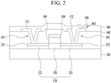
- FIG. 2 is a cross-sectional view illustrating a thin film transistor according to an embodiment of the present disclosure.
- the thin film transistor includes a substrate 120, an active layer 130 disposed on the substrate 120 and including a channel region 131, a source region 132, and a drain region 133, a gate insulation layer 140, and a gate electrode 150.
- the gate insulation layer 140 and the gate electrode 150 are sequentially stacked on the channel region 131.
- the thin film transistor also includes a first diffused portion 231 and a second diffused portion 232 formed at upper portions of the source region 132 and the drain region 133, respectively.
- the thin film transistor also includes an interlayer insulating layer 160 formed on the substrate 120 and on the first and second diffused portions 231 and 232.
- the interlayer insulating layer 160 has a first contact hole 161 and a second contact hole 162 corresponding to the source region 132 and the drain region 133, respectively.
- a source electrode 171 contacts the first diffused portion 231 through the first contact hole 161 and a drain electrode 172 contacts the second diffused portion 232 through the second contact hole 162.
- a passivation layer 180 formed on the interlayer insulating layer 160 has a third contact hole 163 corresponding to an upper surface of the drain electrode 172, and a pixel electrode 190 is connected to the drain electrode 172 through the third contact hole.
- the substrate 120 is a base for forming the thin film transistor.
- the substrate 120 may be formed of silicon, glass, plastic, etc., without being limited thereto.
- the substrate 120 may include a buffer layer thereon.
- the buffer layer prevents diffusion of moisture and impurities generated from the substrate 120.
- the buffer layer is formed as a single layer structure consisting of SiO 2 .
- the buffer layer may be formed as a double-layer structure in which silicon nitride (SiNx) and silicon oxide (SiOx) are sequentially stacked.
- the active layer 130 is formed on the substrate 120.
- the active layer 130 includes the channel region 131 disposed at a center thereof, the source region 132 disposed at one side of the channel region 131, and the drain region 133 disposed at the other side of the channel region 131.
- the channel region 131 overlaps the gate electrode 150 with the gate insulation layer 140 interposed therebetween to form a channel between the source electrode 171 and the drain electrode 172.
- the source region 132 becomes conductive from the metal oxide semiconductor material of the active layer 130, such that the source region 132 is in electrical contact with the source electrode 171 through the first contact hole 161 with the first diffused portion 231 interposed between the source region 131 and the source electrode 171.
- the drain region 133 becomes conductive from the metal oxide semiconductor material of the active layer 130 such that the drain region 133 is in electrical contact with the drain electrode 172 through the second contact hole 162 with the second diffused portion 232 interposed between the drain region 133 and drain electrode 172.
- a group IV metal oxide compound such as an indium tin gallium zinc oxide (InSnGaZnO) material, a group III metal oxide compound such as an indium gallium zinc oxide (InGaZnO) material, an indium tin zinc oxide (InSnZnO) material, an indium aluminum zinc oxide (InAlZnO) material, an indium hafnium zinc oxide (InHfZnO) material, a tin gallium zinc oxide (SnGaZnO) material, an aluminum gallium zinc oxide (AlGaZnO) material, and a tin aluminum zinc oxide (SnAlZnO), a group II metal oxide compound such as an indium zinc oxide (InZnO) material, a tin zinc oxide (SnZnO) material, an aluminum zinc oxide (AlZnO) material, a zinc magnesium oxide (ZnMgO) material, a tin magnesium oxide (SnMgO) material, an indium magnesium oxide (InMg
- Electrical conductivity of the active layer 130 formed of an oxide semiconductor material is decreased as an amount of oxygen or ratio of oxygen is increased.
- electrical conductivity of the active layer 130 is increased as an amount of oxygen or ratio of oxygen is decreased.
- the first and second diffused portions 231 and 232 include the first diffused portion 231 formed at an upper portion of the source region 132 and the second diffused portion 232 formed at an upper portion of the drain region 133.
- the first and second diffused portions 231 and 232 are formed on oxygen-deficient upper portions of the source and drain regions 132 and 133.
- the active layer 130 is formed of the above-described oxide semiconductor.
- the first and second diffused portions 231 and 232 are formed of the same oxide semiconductor material as the active layer 130 the addition of diffusive material, such as Si.
- the diffused portions 231 and 232 may have a greater number or proportion of oxygen vacancies than the remaining portions of the source and drain regions 132 and 133 or the channel region 131. At least a portion of the oxygen vacancies in the diffused portions 231 and 232 may be replaced by the diffusive material, such as Si.
- the diffused portions 231 and 232 are diffused with a first material.
- the diffusive material is Si.
- the diffusive material may include any other material that can replace oxygen vacancies in oxide semiconductor material, such as carbon (C), silicon (Si), Germanium (Ge), Tin (Sn), and the like.
- the first and second diffused portions 231 and 232 containing the Si are formed to contact the interlayer insulating layer 160.
- the first and second diffused portions 231 and 232 can be formed with additional layers in between the interlayer insulating layer 160.
- the source region 132 may have a first diffused portion 231 that includes Si, and a first lower portion below the first diffused portion 231 that does not include Si.
- the drain region 133 may have a second diffused portion 232 that includes Si, and a second lower portion below the second diffused portion 232 that does not include Si.
- the Si may be diffused throughout an entirety of the source region 132 and the drain region 133.
- the oxygen concentration in the first and second diffused portions 231 and 232 is 20% to 80% of the oxygen concentration in a portion of the channel region 131 that does not include Si.
- the oxygen concentration in the first diffused portion 231 may be 20 to 80% of the oxygen concentration in a first lower portion of the source region 132 that is located below the first diffused portion 231.
- the oxygen concentration in the second diffused portion 232 may be 20 to 80% of the oxygen concentration in a second lower portion of the drain region 133 that is located below the second diffused portion 232.
- oxygen concentration refers to the amount of oxygen per unit volume.
- the gate insulation layer 140 When the gate insulation layer 140 is patterned, the at least a region of the source and drain regions 132 and 133 become conductive due to the etchant gas.
- the diffused portions 231 and 232 prevent conductive regions of the source and drain regions 132 and 133 from being oxidized by the deposition of the interlayer insulation layer 160.
- Examples of such etchant gas that create oxygen-deficient portions may be CF 4 or FH 6 but is not limited thereto, and may be any other etchant gas for etching the gate insulation layer 140.
- a Si layer is deposited on the upper surfaces of the source and drain regions 132 and 133 and is heated.
- heating the Si layer may include thermally processing the Si layer.
- Si is diffused into the source and drain regions 132 and 133 and replaces oxygen vacancies.
- Si is diffused for a thickness of approximately 50 ⁇ to 100 ⁇ from the upper surface of the source and drain regions 132 and 133.
- diffusion of oxygen from the interlayer insulating layer 160 formed of SiO 2 throughout the source and drain regions 132 and 133 may be prevented.
- a separate dry etching process is further performed to remove the conductive material on the channel region 131 and pattern the conductive material only on the source and drain regions 132 and 133.
- the channel region 131 may be exposed to the etchant gas to become conductive, thereby losing the function as the channel region 131.
- oxygen of SiO 2 included in the interlayer insulation layer 160 is diffused into the source region 132 and the drain region 133 during formation of the interlayer insulation layer 160, thereby lowering electrical conductivity of the source and drain regions 132 and 133. Accordingly, contact resistance between the source and drain electrodes 171 and 172 and the source and drain regions 132 and 133 is increased and electron mobility is decreased.
- the interlayer insulation layer 160 includes the first contact hole 161 such that the source electrode 171 is electrically connected to at least an exposed portion of the first diffused portion 231 formed at an upper portion of the source region 132. Furthermore, the interlayer insulation layer 160 includes the second contact hole 162 such that the drain electrode 172 is in contact with at least an exposed portion of the second diffused portion 232 formed at an upper portion of the drain region 133.
- the interlayer insulation layer 160 is formed of SiO 2 .
- the first and second diffused portions 231 and 232 are formed by depositing the Si layer on the active layer 130 and heating the deposited Si layer.
- a portion of the Si in the Si layer is diffused into the source region 132 and the drain region 133, and another portion of the Si is oxidized to form a SiO 2 layer.
- the SiO 2 layer formed from an oxidized portion of the Si from the Si layer can be a part of the subsequently deposited interlayer insulation layer 160 that is also formed of SiO 2 .
- SiO 2 formed when forming the diffused portions 231 and 232 does not need to be removed.
- the source electrode 171 is in contact with the first diffused portion 231 of the source region 132 through the first contact hole 161.
- the drain electrode 172 is in contact with the second diffused portion 232 of the drain region 133 through the second contact hole 162.
- Source and drain metal layers may be single layer or multiple layers formed of a metallic material such as Mo, Ti, Cu, AlNd, Al, Cr, or alloys thereof.
- the passivation layer 180 is formed on the interlayer insulation layer 160, the source electrode 171, and the drain electrode 172.
- the passivation layer 180 includes the third contact hole 163 such that a pixel electrode 190 may be connected to the drain electrode 172 below the passivation layer 180.
- the pixel electrode 190 is in contact with the drain electrode 172 through the third contact hole 163.
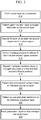
- the active layer 130 is formed 310 on the substrate 120.
- the gate insulation layer 140 and the gate electrode 150 are patterned 312 on the active layer 130.
- the substrate 120 may further include the buffer layer thereon, although not shown in FIG. 4A .
- the oxide semiconductor material is patterned using a photolithography process and an etching process to form the active layer 130.
- the active layer 130 is classified into the channel region 131 at the center thereof, the source region 132 at one side of the channel region 132, and the drain region 133 at the other side of the channel region 131.
- a gate insulting material is formed on the active layer 130 using a chemical vapor deposition (CVD) process and a gate metallic layer is formed on the gate insulting material using a deposition process such as a sputtering process.
- SiO 2 is used as the gate insulting material and a metallic material such as Mo, Ti, Cu, AlNd, Al, Cr or alloys thereof is used as the gate metallic layer.
- the gate insulating material and the gate metallic layer are simultaneously patterned using a photolithography process and a dry etching process to simultaneously form the gate insulation layer 140 and the gate electrode 150 which have the same pattern.
- the gate electrode 150 on the channel region 131 and the source and drain regions 132 and 133 of the active layer 130 are exposed to the etchant gas.
- the channel region 131 is not exposed to the etchant gas by the gate electrode 150 but the source region 132 and the drain region 133 are exposed to the etchant gas such that 85% of oxygen included in an upper portion of the source and drain regions 132 and 133 formed of oxide semiconductor is released and thus, the upper portions of the source and drain regions 132 and 133 become conductive.
- the number or proportion of oxygen vacancies in the upper portions of the source and drain regions 132 and 133 may be greater than that of the channel region 131.
- a Si layer 240 is deposited 314 on at least the source region 132 and the drain region 133 of the active layer 130.
- Si is added into the source region 132 and the drain region 133 to form the first and second diffused portions 231 and 232.
- a heating process is performed 316 to diffuse the Si into first and second diffused portions 231 and 232.
- Diffusing Si is an example of adding Si into the first and second diffused portions 231 and 232, but other methods of adding Si may also be performed.
- the first and second diffused portions 231 and 232 are formed into conductive portions of the source and drain regions 132 and 133 such that diffusion of oxygen from the interlayer insulation layer 160 formed of SiO 2 is prevented.
- the source region 132 may include the diffused portion 231 containing Si and a first lower portion below the diffused portion 231 without Si.
- the drain region 133 may include the diffused portion 232 containing Si and a second lower portion below the diffused portion 232 without Si.
- the oxygen concentration in the first diffused portion 231 is 20% to 80% of the oxygen concentration in the channel region 131.
- the oxygen concentration in the second diffused portion 232 is 20 to 80% of the oxygen concentration of the channel region 131.
- Si is diffused into the upper portions of the source and drain regions 231 and 232 to replace oxygen vacancies.
- the oxygen concentration in the first diffused portion 231 may be 20 to 80% of the oxygen concentration in a first lower portion of the source region 132 located below the first diffused portion 231.
- the oxygen concentration in the second diffused portion 232 may be 20 to 80% of the oxygen concentration in a second lower portion of the drain region 133 located below the second diffused portion 232.
- the Si layer 240 is deposited on the active layer 130 and the gate electrode 150 to have a thickness of 30 ⁇ to 50 ⁇ .
- the heating process is performed. After heating, Si is diffused from the Si layer 240 into the source and drain regions 132 and 133 to form the first and second diffused portions 231 and 232. In one embodiment, the amount of Si diffused into the source and drain regions 132 and 133 is from 1 ⁇ 10 22 atoms/cm 3 to 4 ⁇ 10 22 atoms/cm 3 .
- the Si layer 240 formed at the upper part of the gate electrode 150 is oxidized and is converted into a SiO 2 layer 241.
- the SiO 2 layer 241 becomes a part of the interlayer insulation layer 160.
- a SiO 2 layer which is formed from Si that was oxidized but not diffused into the source and drain regions 132 and 133, may be formed on the source region 132 and the drain region 133.
- the SiO 2 formed from oxidation becomes a part of the interlayer insulation layer 160 which will be formed in one or more subsequent processes. Accordingly, there is no a separate process for removal of SiO 2 .
- the necessary thickness of each of first and second diffused portions 231 and 232 of the source and drain regions 132 and 133 is about 100 ⁇ .
- a thickness of the Si layer 240 is below 30 ⁇ , the corresponding formed diffused portions do not have a thickness of 50 to 100 ⁇ in spite of the diffusion of Si using the heating process.
- a thickness of the Si layer 240 is above 50 ⁇ , the Si layer 240 is not entirely converted to SiO 2 but a portion of the Si layer 240 remains after the heating process. Accordingly, the thickness of the Si layer 240 deposited on the active layer 130 may be 30 to 50 ⁇ .
- the interlayer insulation layer 160 formed of SiO 2 on the active layer 130 supplies oxygen to the oxygen-deficient portions of the source and drain regions 132 and 133 of the active layer 130 to decrease electron mobility of the source and drain regions 132 and 133 of the active layer 130.
- the source electrode 171 and the drain electrode 172 are formed at the source and drain regions 132 and 133 to which oxygen is supplied, respectively, contact resistance between the source region 132 and the source electrode 171 and contact resistance between the drain region 133 and the drain electrode 172 are increased. Thereby, electron mobility decreases and properties of the thin film transistor are diminished.
- an interlayer insulation layer 160 is deposited 318 on the gate electrode 150 and the first and second diffused portions 231 and 232.
- First and second contact holes 161 and 162 are patterned 320 in the interlayer insulating layer 160.
- the interlayer insulation layer 160 is formed on the substrate 120 on which the gate electrode 150 is formed using plasma enhanced CVD (PECVD). Then, as illustrated in FIG. 4E , the interlayer insulation layer 160 is patterned using a photolithography process and an etching process to form the first and second contact holes 161 and 162.
- the first contact hole 161 passes through the interlayer insulation layer 160 to expose at least a portion of the first diffused portion 231 of the source region 132.
- the second contact hole 162 passes through the interlayer insulation layer 160 to expose at least a portion of the second diffused portion 232 of the drain region 133.
- the oxygen concentration in the first and second diffused portions 231 and 232 may be 20 to 80% of the oxygen concentration of the channel region 131 to maintain good conductivity.
- the source electrode 171 and the drain electrode 172 are patterned 322 on the interlayer insulation layer 160.
- a source and drain metallic layer is formed on the interlayer insulation layer 160 having the first and second contact holes 161 and 162 using a deposition method such as a sputtering process.
- the source and drain metallic layer is formed of Mo, Ti, Cu, AlNd, Al, Cr or alloys thereof to have a single layer or multilayer structure.
- the source and drain metallic layer is patterned by a photolithography process and an etching process to form the source electrode 171 and the drain electrode 172 on the interlayer insulation layer 160.
- the passivation layer 180 is formed 324 on the interlayer insulation layer 160 at which the source electrode 171 and the drain electrode 172 are formed.
- the third contact hole 163 is formed through the passivation layer 180 such that the pixel electrode 190 is in contact with the drain electrode 172.
- the pixel electrode 190 being in contact with the drain electrode 172 is formed through the third contact hole 163.
- IGZO indium gallium zinc oxide
- SiO 2 used as the buffer layer and the interlayer insulation layer
- the oxide semiconductor is not limited to indium gallium zinc oxide (IGZO).
- Table 1 is a table explaining the oxygen concentration difference according to whether the diffused portions are present or not present, using a quantitative composition analysis such as Rutherford backscattering spectrometry (RBS).
- RBS Rutherford backscattering spectrometry
- the oxygen concentration in the source and drain regions 231 and 232 before forming the gate insulation layer 140 is 4.8x10 22 atoms/cm 3 .
- the oxygen concentration in the source and drain regions 132 and 133 is 7x10 21 atoms/cm 3 after performing a dry etching process. During the dry etching process, the source and drain regions 132 and 133 become conductive due to releasing 85% of the oxygen concentration in the source and drain regions 132 and 133 with 15% remaining, and is therefore oxygen-deficient.
- the oxygen concentration included in the upper portions of the source and drain regions 132 and 133 is above 4.3x10 22 atoms/cm 3 . This means that the oxygen concentration in the source and drain regions 132 and 133 is recovered by 90% or more of its original concentration before forming the gate insulating layer 140.
- the oxygen concentration included in the diffused portions 231 and 232 is 1x10 22 atoms/cm 3 to 4x10 22 atoms/cm 3 . This means that the oxygen concentration of the source and drain regions 132 and 133 is recovered by 15% to 80% of the oxygen concentration of the source and drain regions 132 and 133 before the gate insulation layer 140 is formed.
- the oxygen concentration at the surface of the source and drain regions 132 and 133 is recovered by above 90% of the oxygen concentration in the source and drain regions 132 and 133 before the gate insulation layer 140 is formed, thereby decreasing electron mobility of the device.
- the oxygen concentration included in the diffused portions 231 and 232 disposed at upper portions of the source and drain regions 132 and 133 may be decreased by 10 to 80%.
- FIG. 5A is a graph illustrating properties of the thin film transistor without the diffused portion.
- FIG. 5B is a graph illustrating properties of the thin film transistor with the diffused portion.
- Table 2 is a table explaining electron mobility (UFE) and sheet resistance according to whether the diffused portions are present or not. [Table 2] Without diffused portion With diffused portion Vth 2.55 0.48 UFE [cm 2 /Vs] 4.3 10.4 Sheet Resistance [k ⁇ / ⁇ ] 68.5 2.32
- Table 3 is a table explaining electron mobility and sheet resistance before or after a heating process when the diffused portions are formed by diffusion of hydrogen (H) into the conductive regions, instead of Si. [Table 3] Before heating After heating UFE [cm 2 /Vs] 11 9 Sheet Resistance [k ⁇ / ⁇ ] 2.17 7.4
- electron mobility and sheet resistance of the H-diffused oxidation protection layer is the same as the electron mobility and sheet resistance of the Si-diffused oxidation protection layer, respectively.
- electron mobility is 10.4 cm 2 /Vs and sheet resistance is 2.32 k ⁇ / ⁇ , which is a higher electron mobility and lower sheet resistance in comparison with the H-diffused portion.
- diffusion of Si may generate a conductive region that is more thermally-stable than that created by diffusion of H.
- the first and second diffused portions 231 and 232 in which Si is diffused into the active layer 130 are provided at the source region 132 and the drain region 133 using the above-described manufacturing method and, as such, the oxygen concentration in the diffused portions 231 and 232 may remain low, that is, 20 to 80% of the oxygen concentration in the channel region 131. Thereby, thermally-stable conductive regions may be secured.
- Table 4 is a table explaining sheet resistance according to the amount of Si diffused into the source and drain regions.
- the sheet resistance when the amount of Si diffused into the source and drain regions is more than 4 ⁇ 10 22 , the sheet resistance is increased to more than 10 k ⁇ / ⁇ . Also, when the amount of Si diffused into the source and drain regions is less than 1 ⁇ 10 22 , the sheet resistance can be increased to more than 5 k ⁇ / ⁇ in most positions, with the exception of one position that has a sheet resistance of 3.4 k ⁇ / ⁇ . However, when the amount of Si diffused into the source and drain regions is from 1 ⁇ 10 22 to 4 ⁇ 10 22 , the sheet resistance may maintain a low level being less than 5 k ⁇ / ⁇ .
- the thin film transistor according to the illustrated embodiment of the present invention is applied to a display device such as a liquid crystal display device and an organic electric-field light emitting device, or a switching device of a driving circuit such as a gate driver formed on the substrate.
- a display device such as a liquid crystal display device and an organic electric-field light emitting device
- a switching device of a driving circuit such as a gate driver formed on the substrate.
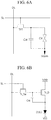
- the thin film transistor according to the illustrated embodiment of the present disclosure can be applied to the liquid crystal display device to operate a liquid crystal cell Clc.
- the thin film transistor TFT is turned on by a gate-on-voltage from a scan line SL to supply a data signal of a data line DL to the pixel electrode of the liquid crystal cell Clc.
- the liquid crystal cell Clc receives a difference between a common voltage Vcom supplied to a common electrode and the data signal.
- the liquid crystal cell Clc maintains a voltage applied to the liquid crystal cell Clc when the thin film transistor is turned off by a gate off voltage.
- the liquid crystal cell Clc operates liquid crystal molecules according to the applied voltage to adjust light transmittance thereby displaying an image.
- the thin film transistor according to the illustrated embodiment of the present disclosure can be applied to the organic electric-field light emitting device as a driving transistor Tr_D and a switching transistor Tr_Sw for operating an organic light-emitting diode OLED.
- the switching transistor Tr_Sw responds to a gate voltage supplied through a scan line SL to perform a switching operation in which a data signal supplied through a data line DL is stored in a storage capacitor Cst as a data voltage.
- the driving transistor Tr_D allows driving current to flow between a high voltage line VDD and a low voltage line VSS according to the data voltage stored in the storage capacitor Cst.
- the organic light emitting diode OLED includes an anode electrode connected to the driving transistor Tr_D and a cathode electrode facing the anode electrode, in which a light emitting layer is interposed therebetween.
- the organic light emitting diode OLED operates to emit light according to driving current formed by the driving transistor Tr_D.
- the thin film transistor includes first and second diffused portions having Si replacing oxygen vacancies at the source and drain regions to prevent oxygen from being supplied to the conductive regions from the interlayer insulation layer to lower contact resistance between the source and drain electrodes and the active layer, and to secure heat-stable conductive regions.
- properties of the thin film transistor may be improved.
Landscapes
- Physics & Mathematics (AREA)
- Engineering & Computer Science (AREA)
- Nonlinear Science (AREA)
- Microelectronics & Electronic Packaging (AREA)
- Mathematical Physics (AREA)
- Crystallography & Structural Chemistry (AREA)
- Chemical & Material Sciences (AREA)
- General Physics & Mathematics (AREA)
- Optics & Photonics (AREA)
- Geometry (AREA)
- Thin Film Transistor (AREA)
- Manufacturing & Machinery (AREA)
- Devices For Indicating Variable Information By Combining Individual Elements (AREA)
Abstract
Description
- The present disclosure relates to a thin film transistor, a method of fabricating the same, and a display device including the same, and more particularly, to a thin film transistor with improved device characteristics, a display device including the same, and a method of fabricating the same.
- A display device that displays various information on a screen is a core technology of the information technology age. The display device is developed to become thin, light, portable, and high-functionality. To this end, a flat display device has been of interest since weight and volume, which are a disadvantages of cathode ray tubes (CRTs), are reduced.
- The flat display device includes thin film transistors disposed on every pixel which is disposed on a display panel for displaying an image. Thin film transistors may be classified into various types according to various positions of a gate electrode, a source electrode, and an active layer.
-
FIG. 1 is a cross-sectional view illustrating a conventional thin film transistor having a coplanar structure. - Referring to
FIG. 1 , the thin film transistor of the coplanar structure includes agate electrode 15, agate insulation layer 14, adrain electrode 17, and asource electrode 18 on anactive layer 20. - A process of patterning a
gate insulation layer 14 and thegate electrode 15 on theactive layer 20 includes a dry etching process. Achannel region 21 of theactive layer 20 is protected from an etchant gas by thegate electrode 15 during the dry etching process, but upper surfaces of asource region 22 and adrain region 23 of theactive layer 20 are exposed to the etchant gas. - Herein, portions having a thickness of 100Å from the upper surfaces of the
source region 22 and thedrain region 23 are damaged by the etchant gas, and lose oxygen and become an oxygen-deficient state. The oxygen-deficient source anddrain regions - Meanwhile, an
interlayer insulation layer 16 is formed on the conductive source anddrain regions interlayer insulation layer 16 of SiO2 covers the conductive regions, oxygen in SiO2 is diffused into the source anddrain regions drain regions source region 22 and thesource electrode 18, and thedrain region 23 and thedrain electrode 17 is increased, and properties of the thin film transistor are degraded. - Accordingly, an embodiment of the present disclosure is directed to a thin film transistor, a display device including the same and a method of fabricating the same that substantially obviates one or more problems due to limitations and disadvantages of the related art.
- An object of the present disclosure is to provide a thin film transistor improving properties thereof and a display device including the same by preventing diffusion of oxygen from an interlayer insulation layer into the conductive source/drain regions for maintaining conductivity of source/drain regions and lowering contact resistance between the source/drain regions and source/drain electrodes.
- Additional advantages, objects, and features of the disclosure will be set forth in part in the description which follows and in part will become apparent to those having ordinary skill in the art upon examination of the following or may be learned from practice of the disclosure. The objectives and other advantages of the disclosure may be realized and attained by the structure particularly pointed out in the written description and claims hereof as well as the appended drawings.
- In accordance with an embodiment of the present disclosure, the above and other objects can be accomplished by the provision of a thin film transistor including an active layer on a substrate, the active layer including a source region, a drain region and a channel region between the source region and the drain region, a gate insulation layer and a gate electrode sequentially stacked on the channel region, oxidation protection layers formed at the source and drain regions, respectively, an interlayer insulation layer on a buffer layer and the oxidation protection layers, the interlayer insulation layer having first and second contact holes corresponding to the source and drain regions, respectively, and a source electrode and a drain electrode contacting the oxidation protection layers through the first and second contact holes, respectively.
- The oxidation protection layers may be disposed on a surface the active layer by diffusing Si the same material as the material of the active layer.
- The oxidation protection layers may have a thickness of 50 to 100Å.
- Embodiments also relate to a thin film transistor. The thin film transistor includes a gate electrode and an active layer of oxide semiconductor on a substrate. The active layer includes a channel region corresponding to the gate electrode, a source region at one side of the channel region, and a drain region at the other side of the channel region. The source region includes a first upper portion that includes the oxide semiconductor and Si, and the drain region includes a second upper portion that includes the oxide semiconductor and Si.
- Embodiments also relate to a method of manufacturing a thin film transistor. An active layer of oxide semiconductor is formed on a substrate. The active layer includes a channel region, a source region at one side of the channel region, and a drain region at the other side of the channel region. Si is added into a first upper portion of the source region and a second upper portion of the drain region.
- It is to be understood that both the foregoing general description and the following detailed description of the present disclosure are exemplary and explanatory and are intended to provide further explanation of the invention as claimed.
- The accompanying drawings, which are included to provide a further understanding of the disclosure and are incorporated in and constitute a part of this application, illustrate embodiment(s) of the disclosure and together with the description serve to explain the principle of the disclosure. In the drawings:
-
FIG. 1 is a cross-sectional view illustrating a conventional thin film transistor having a coplanar structure. -
FIG. 2 is a cross-sectional view illustrating a thin film transistor according to an embodiment of the present disclosure. -
FIG. 3 is a flowchart illustrating a method of manufacturing the thin film transistor according to the illustrated embodiment of the present disclosure. -
FIGs. 4A to 4G are cross-sectional views illustrating the method of manufacturing the thin film transistor according to the illustrated embodiment of the present disclosure. -
FIG. 5A is a graph illustrating properties of a thin film transistor without an oxidation protection layer, andFIG. 5B is a graph illustrating properties of a thin film transistor without the oxidation protection layer. -
FIG. 6A is a view illustrating a liquid crystal display device to which the thin film transistor according to an embodiment of the present disclosure is applied, andFIG. 6B is a view illustrating an organic electroluminescence display device according to an embodiment of the present disclosure. - Hereinafter, reference will be made in detail to embodiments of the disclosure, examples of which are illustrated in the accompanying drawings.
-
FIG. 2 is a cross-sectional view illustrating a thin film transistor according to an embodiment of the present disclosure. - Referring to
FIG. 2 , the thin film transistor according to the embodiment of the present disclosure includes asubstrate 120, anactive layer 130 disposed on thesubstrate 120 and including achannel region 131, asource region 132, and adrain region 133, agate insulation layer 140, and agate electrode 150. Thegate insulation layer 140 and thegate electrode 150 are sequentially stacked on thechannel region 131. The thin film transistor also includes a first diffusedportion 231 and a second diffusedportion 232 formed at upper portions of thesource region 132 and thedrain region 133, respectively. The thin film transistor also includes aninterlayer insulating layer 160 formed on thesubstrate 120 and on the first and second diffusedportions interlayer insulating layer 160 has afirst contact hole 161 and asecond contact hole 162 corresponding to thesource region 132 and thedrain region 133, respectively. Asource electrode 171 contacts the first diffusedportion 231 through thefirst contact hole 161 and adrain electrode 172 contacts the second diffusedportion 232 through thesecond contact hole 162. Apassivation layer 180 formed on theinterlayer insulating layer 160 has athird contact hole 163 corresponding to an upper surface of thedrain electrode 172, and apixel electrode 190 is connected to thedrain electrode 172 through the third contact hole. - The
substrate 120 is a base for forming the thin film transistor. Thesubstrate 120 may be formed of silicon, glass, plastic, etc., without being limited thereto. - Meanwhile, although not shown in
FIG. 2 , thesubstrate 120 may include a buffer layer thereon. The buffer layer prevents diffusion of moisture and impurities generated from thesubstrate 120. The buffer layer is formed as a single layer structure consisting of SiO2. Alternatively, the buffer layer may be formed as a double-layer structure in which silicon nitride (SiNx) and silicon oxide (SiOx) are sequentially stacked. - The
active layer 130 is formed on thesubstrate 120. Theactive layer 130 includes thechannel region 131 disposed at a center thereof, thesource region 132 disposed at one side of thechannel region 131, and thedrain region 133 disposed at the other side of thechannel region 131. - The
channel region 131 overlaps thegate electrode 150 with thegate insulation layer 140 interposed therebetween to form a channel between thesource electrode 171 and thedrain electrode 172. Thesource region 132 becomes conductive from the metal oxide semiconductor material of theactive layer 130, such that thesource region 132 is in electrical contact with thesource electrode 171 through thefirst contact hole 161 with the first diffusedportion 231 interposed between thesource region 131 and thesource electrode 171. Thedrain region 133 becomes conductive from the metal oxide semiconductor material of theactive layer 130 such that thedrain region 133 is in electrical contact with thedrain electrode 172 through thesecond contact hole 162 with the second diffusedportion 232 interposed between thedrain region 133 anddrain electrode 172. - A group IV metal oxide compound such as an indium tin gallium zinc oxide (InSnGaZnO) material, a group III metal oxide compound such as an indium gallium zinc oxide (InGaZnO) material, an indium tin zinc oxide (InSnZnO) material, an indium aluminum zinc oxide (InAlZnO) material, an indium hafnium zinc oxide (InHfZnO) material, a tin gallium zinc oxide (SnGaZnO) material, an aluminum gallium zinc oxide (AlGaZnO) material, and a tin aluminum zinc oxide (SnAlZnO), a group II metal oxide compound such as an indium zinc oxide (InZnO) material, a tin zinc oxide (SnZnO) material, an aluminum zinc oxide (AlZnO) material, a zinc magnesium oxide (ZnMgO) material, a tin magnesium oxide (SnMgO) material, an indium magnesium oxide (InMgO) material, an indium gallium oxide (InGaO) material, or an indium oxide (InO) material, a tin oxide (SnO) material, and a zinc oxide (ZnO) material may be used as the
active layer 130. A ratio of composition of each element included in a material for oxide semiconductor in theactive layer 130 may be not limited but may be variously adjusted. - Electrical conductivity of the
active layer 130 formed of an oxide semiconductor material is decreased as an amount of oxygen or ratio of oxygen is increased. On the other hand, electrical conductivity of theactive layer 130 is increased as an amount of oxygen or ratio of oxygen is decreased. - The first and second diffused
portions portion 231 formed at an upper portion of thesource region 132 and the second diffusedportion 232 formed at an upper portion of thedrain region 133. - The first and second diffused
portions regions active layer 130 is formed of the above-described oxide semiconductor. The first and second diffusedportions active layer 130 the addition of diffusive material, such as Si. Specifically, the diffusedportions regions channel region 131. At least a portion of the oxygen vacancies in the diffusedportions portions - In one particular example referred throughout the remainder of the specification, the diffusive material is Si. However, it is appreciated that in other examples, the diffusive material may include any other material that can replace oxygen vacancies in oxide semiconductor material, such as carbon (C), silicon (Si), Germanium (Ge), Tin (Sn), and the like.
- The first and second diffused
portions interlayer insulating layer 160. Alternatively, the first and second diffusedportions layer 160. Moreover, when the diffusedportions source region 132 and thedrain region 133, respectively, thesource region 132 may have a first diffusedportion 231 that includes Si, and a first lower portion below the first diffusedportion 231 that does not include Si. Similarly, thedrain region 133 may have a second diffusedportion 232 that includes Si, and a second lower portion below the second diffusedportion 232 that does not include Si. Alternatively, when thesource region 132 and thedrain region 133 are relatively thin, the Si may be diffused throughout an entirety of thesource region 132 and thedrain region 133. - The oxygen concentration in the first and second diffused
portions channel region 131 that does not include Si. The oxygen concentration in the first diffusedportion 231 may be 20 to 80% of the oxygen concentration in a first lower portion of thesource region 132 that is located below the first diffusedportion 231. Similarly, the oxygen concentration in the second diffusedportion 232 may be 20 to 80% of the oxygen concentration in a second lower portion of thedrain region 133 that is located below the second diffusedportion 232. As defined herein, oxygen concentration refers to the amount of oxygen per unit volume. - When the
gate insulation layer 140 is patterned, the at least a region of the source and drainregions portions regions interlayer insulation layer 160. - Specifically, when the
gate insulation layer 140 and thegate electrode 150 are patterned, upper portions near the surface of the source and drainregions regions regions regions - Examples of such etchant gas that create oxygen-deficient portions may be CF4 or FH6 but is not limited thereto, and may be any other etchant gas for etching the
gate insulation layer 140. - In an embodiment of the present disclosure, a Si layer is deposited on the upper surfaces of the source and drain
regions regions regions layer 160 formed of SiO2 throughout the source and drainregions - Meanwhile, when a layer of conductive material such as a metal are formed instead of the formation of diffused
portions channel region 131 and pattern the conductive material only on the source and drainregions channel region 131 may be exposed to the etchant gas to become conductive, thereby losing the function as thechannel region 131. - If there are no diffused
portions interlayer insulation layer 160 is diffused into thesource region 132 and thedrain region 133 during formation of theinterlayer insulation layer 160, thereby lowering electrical conductivity of the source and drainregions electrodes regions - The
interlayer insulation layer 160 includes thefirst contact hole 161 such that thesource electrode 171 is electrically connected to at least an exposed portion of the first diffusedportion 231 formed at an upper portion of thesource region 132. Furthermore, theinterlayer insulation layer 160 includes thesecond contact hole 162 such that thedrain electrode 172 is in contact with at least an exposed portion of the second diffusedportion 232 formed at an upper portion of thedrain region 133. - The
interlayer insulation layer 160 is formed of SiO2. The first and second diffusedportions active layer 130 and heating the deposited Si layer. - Herein, a portion of the Si in the Si layer is diffused into the
source region 132 and thedrain region 133, and another portion of the Si is oxidized to form a SiO2 layer. The SiO2 layer formed from an oxidized portion of the Si from the Si layer can be a part of the subsequently depositedinterlayer insulation layer 160 that is also formed of SiO2. Thus, SiO2 formed when forming the diffusedportions - The
source electrode 171 is in contact with the first diffusedportion 231 of thesource region 132 through thefirst contact hole 161. Thedrain electrode 172 is in contact with the second diffusedportion 232 of thedrain region 133 through thesecond contact hole 162. - Source and drain metal layers may be single layer or multiple layers formed of a metallic material such as Mo, Ti, Cu, AlNd, Al, Cr, or alloys thereof.
- The
passivation layer 180 is formed on theinterlayer insulation layer 160, thesource electrode 171, and thedrain electrode 172. Thepassivation layer 180 includes thethird contact hole 163 such that apixel electrode 190 may be connected to thedrain electrode 172 below thepassivation layer 180. - The
pixel electrode 190 is in contact with thedrain electrode 172 through thethird contact hole 163. - Hereinafter, a method of manufacturing the thin film transistor will be explained in detail with reference to the accompanying
FIG. 3 andFIGs. 4A to 4G . - As illustrated in
FIGs. 3 and4A , theactive layer 130 is formed 310 on thesubstrate 120. In addition, thegate insulation layer 140 and thegate electrode 150 are patterned 312 on theactive layer 130. Herein, thesubstrate 120 may further include the buffer layer thereon, although not shown inFIG. 4A . - In detail, after an oxide semiconductor material, as described above, is entirely deposited on the
substrate 120 using a sputtering process, the oxide semiconductor material is patterned using a photolithography process and an etching process to form theactive layer 130. Theactive layer 130 is classified into thechannel region 131 at the center thereof, thesource region 132 at one side of thechannel region 132, and thedrain region 133 at the other side of thechannel region 131. - A gate insulting material is formed on the
active layer 130 using a chemical vapor deposition (CVD) process and a gate metallic layer is formed on the gate insulting material using a deposition process such as a sputtering process. SiO2 is used as the gate insulting material and a metallic material such as Mo, Ti, Cu, AlNd, Al, Cr or alloys thereof is used as the gate metallic layer. Sequentially, the gate insulating material and the gate metallic layer are simultaneously patterned using a photolithography process and a dry etching process to simultaneously form thegate insulation layer 140 and thegate electrode 150 which have the same pattern. - In the dry etching process for patterning the
gate electrode 150 and thegate insulation layer 140, thegate electrode 150 on thechannel region 131 and the source and drainregions active layer 130 are exposed to the etchant gas. Herein, thechannel region 131 is not exposed to the etchant gas by thegate electrode 150 but thesource region 132 and thedrain region 133 are exposed to the etchant gas such that 85% of oxygen included in an upper portion of the source and drainregions regions regions channel region 131. - As illustrated in
FIGs. 3 ,4B , and4C , after aSi layer 240 is deposited 314 on at least thesource region 132 and thedrain region 133 of theactive layer 130. Si is added into thesource region 132 and thedrain region 133 to form the first and second diffusedportions portions portions portions regions interlayer insulation layer 160 formed of SiO2 is prevented. Thus, thesource region 132 may include the diffusedportion 231 containing Si and a first lower portion below the diffusedportion 231 without Si. Thedrain region 133 may include the diffusedportion 232 containing Si and a second lower portion below the diffusedportion 232 without Si. - The oxygen concentration in the first diffused
portion 231 is 20% to 80% of the oxygen concentration in thechannel region 131. The oxygen concentration in the second diffusedportion 232 is 20 to 80% of the oxygen concentration of thechannel region 131. In other words, Si is diffused into the upper portions of the source and drainregions portion 231 may be 20 to 80% of the oxygen concentration in a first lower portion of thesource region 132 located below the first diffusedportion 231. The oxygen concentration in the second diffusedportion 232 may be 20 to 80% of the oxygen concentration in a second lower portion of thedrain region 133 located below the second diffusedportion 232. - In detail, as illustrated in
FIG. 4B , theSi layer 240 is deposited on theactive layer 130 and thegate electrode 150 to have a thickness of 30Å to 50Å. - As illustrated in
FIG. 4C , the heating process is performed. After heating, Si is diffused from theSi layer 240 into the source and drainregions portions regions - Furthermore, the
Si layer 240 formed at the upper part of thegate electrode 150 is oxidized and is converted into a SiO2 layer 241. Thereby, the SiO2 layer 241 becomes a part of theinterlayer insulation layer 160. Meanwhile, a SiO2 layer, which is formed from Si that was oxidized but not diffused into the source and drainregions source region 132 and thedrain region 133. Like thechannel region 131, the SiO2 formed from oxidation becomes a part of theinterlayer insulation layer 160 which will be formed in one or more subsequent processes. Accordingly, there is no a separate process for removal of SiO2. - The necessary thickness of each of first and second diffused
portions regions Si layer 240 is below 30Å, the corresponding formed diffused portions do not have a thickness of 50 to 100Å in spite of the diffusion of Si using the heating process. When a thickness of theSi layer 240 is above 50Å, theSi layer 240 is not entirely converted to SiO2 but a portion of theSi layer 240 remains after the heating process. Accordingly, the thickness of theSi layer 240 deposited on theactive layer 130 may be 30 to 50Å. - When first and second diffused
portions interlayer insulation layer 160 formed of SiO2 on theactive layer 130 supplies oxygen to the oxygen-deficient portions of the source and drainregions active layer 130 to decrease electron mobility of the source and drainregions active layer 130. When thesource electrode 171 and thedrain electrode 172 are formed at the source and drainregions source region 132 and thesource electrode 171 and contact resistance between thedrain region 133 and thedrain electrode 172 are increased. Thereby, electron mobility decreases and properties of the thin film transistor are diminished. - As illustrated in
FIGs. 3 ,4D and4E , aninterlayer insulation layer 160 is deposited 318 on thegate electrode 150 and the first and second diffusedportions interlayer insulating layer 160. - In detail, as illustrated in
FIG. 4D , theinterlayer insulation layer 160 is formed on thesubstrate 120 on which thegate electrode 150 is formed using plasma enhanced CVD (PECVD). Then, as illustrated inFIG. 4E , theinterlayer insulation layer 160 is patterned using a photolithography process and an etching process to form the first and second contact holes 161 and 162. Herein, thefirst contact hole 161 passes through theinterlayer insulation layer 160 to expose at least a portion of the first diffusedportion 231 of thesource region 132. Thesecond contact hole 162 passes through theinterlayer insulation layer 160 to expose at least a portion of the second diffusedportion 232 of thedrain region 133. - As described above, at least a portion of vacancies where oxygen is released are replaced with Si to form the Si-diffused first and second diffused
portions interlayer insulation layer 160. Accordingly, the oxygen concentration in the first and second diffusedportions channel region 131 to maintain good conductivity. - In the case that no first and second diffused
portions interlayer insulation layer 160, oxygen is diffused into the conductive portions of the source and drainregions channel region 131, and the oxygen concentration in these portions of the source and drainregions channel region 131. Thereby, the source and drainregions - As illustrated in
FIGs. 3 and4F , thesource electrode 171 and thedrain electrode 172 are patterned 322 on theinterlayer insulation layer 160. - In detail, a source and drain metallic layer is formed on the
interlayer insulation layer 160 having the first and second contact holes 161 and 162 using a deposition method such as a sputtering process. The source and drain metallic layer is formed of Mo, Ti, Cu, AlNd, Al, Cr or alloys thereof to have a single layer or multilayer structure. Then, the source and drain metallic layer is patterned by a photolithography process and an etching process to form thesource electrode 171 and thedrain electrode 172 on theinterlayer insulation layer 160. - As illustrated in
FIGs. 3 and4G , thepassivation layer 180 is formed 324 on theinterlayer insulation layer 160 at which thesource electrode 171 and thedrain electrode 172 are formed. Thethird contact hole 163 is formed through thepassivation layer 180 such that thepixel electrode 190 is in contact with thedrain electrode 172. In addition, thepixel electrode 190 being in contact with thedrain electrode 172 is formed through thethird contact hole 163. - Hereinafter, in Tables 1 to 4, samples including indium gallium zinc oxide (IGZO) used as the oxide semiconductor and SiO2 used as the buffer layer and the interlayer insulation layer were measured for oxygen amounts. However, the oxide semiconductor is not limited to indium gallium zinc oxide (IGZO).
- Table 1 is a table explaining the oxygen concentration difference according to whether the diffused portions are present or not present, using a quantitative composition analysis such as Rutherford backscattering spectrometry (RBS).
[Table 1] With diffused portion Without diffused portion Oxygen concentration in source/drain regions before forming gate insulation layer 4.8x10²² atoms/cm3 (100%) 4.8x10²² atoms /cm3(100%) Oxygen concentration in source/drain regions after forming gate insulation layer 7x10²¹ atoms/cm3 (15%) 7x10²¹ atoms /cm3 (15%) Oxygen concentration in source/drain regions after forming interlayer insulation layer 1x10²² atoms/cm3 to 4x10²²/cm3 (20 to 80%) 4.3x10²² atoms/cm3 (90%) - The oxygen concentration in the source and drain
regions gate insulation layer 140 is 4.8x10²² atoms/cm3. In addition, upon formation of thegate insulation layer 140, the oxygen concentration in the source and drainregions regions regions - When the
interlayer insulation layer 160 is formed without the first and second diffusedportions regions regions gate insulating layer 140. - When the first and second diffused
portions portions regions regions gate insulation layer 140 is formed. - Namely, when the
interlayer insulation layer 160 is formed without the diffusedportions regions regions gate insulation layer 140 is formed, thereby decreasing electron mobility of the device. However, when the diffusedportions portions regions -
FIG. 5A is a graph illustrating properties of the thin film transistor without the diffused portion.FIG. 5B is a graph illustrating properties of the thin film transistor with the diffused portion. Table 2 is a table explaining electron mobility (UFE) and sheet resistance according to whether the diffused portions are present or not.[Table 2] Without diffused portion With diffused portion Vth 2.55 0.48 UFE [cm2/Vs] 4.3 10.4 Sheet Resistance [kΩ/□] 68.5 2.32 - Referring to Table 2 and
FIG. 5A , when there are no diffused portions, electron mobility is 4.3 cm2/Vs and sheet resistance is 68.5 kΩ/□. However, referring to Table 2 andFIG. 5B , when there are diffused portions, electron mobility is 10.4 cm2/Vs and sheet resistance is 2.32 kΩ/□. Namely, due to the diffused portions, electron mobility may be improved and sheet resistance may be decreased. The diffused portions may be used for formation of ohmic contact upon contact with metal. - Table 3 is a table explaining electron mobility and sheet resistance before or after a heating process when the diffused portions are formed by diffusion of hydrogen (H) into the conductive regions, instead of Si.
[Table 3] Before heating After heating UFE [cm2/Vs] 11 9 Sheet Resistance [kΩ/□] 2.17 7.4 - Before the heating process, electron mobility and sheet resistance of the H-diffused oxidation protection layer is the same as the electron mobility and sheet resistance of the Si-diffused oxidation protection layer, respectively.
- However, after the heating process, electron mobility of the H-diffused oxidation protection layer is decreased
form 11 cm2/Vs to 9 cm2/Vs and sheet resistance of the H-diffused oxidation protection layer is increased from 2.17 kΩ/□ to 7.4 kΩ/□. When the H-diffused oxidation protection layer is formed, the oxidation protection layer is vulnerable to heat, and the electron mobility is decreased and the sheet resistance is increased upon the heating process. - In the case of the Si-diffused portion according to the illustrated embodiment of the present disclosure, electron mobility is 10.4 cm2/Vs and sheet resistance is 2.32 kΩ/□, which is a higher electron mobility and lower sheet resistance in comparison with the H-diffused portion. Namely, diffusion of Si may generate a conductive region that is more thermally-stable than that created by diffusion of H.
- Namely, the first and second diffused
portions active layer 130 are provided at thesource region 132 and thedrain region 133 using the above-described manufacturing method and, as such, the oxygen concentration in the diffusedportions channel region 131. Thereby, thermally-stable conductive regions may be secured.Table 4 is a table explaining sheet resistance according to the amount of Si diffused into the source and drain regions. The amount of Si diffused into the source and drain regions [atoms/cm3] Sheet Resistance according to position [kΩ/□] 1 2 3 4 5 More than 4×10²² More than 10 1×10²² ∼ 4×10²² 3.5 2.5 4.1 4.5 3 3.3 2.4 3.7 4.3 2.7 3.5 2.5 4.4 4.7 3 3.8 2.6 3.9 4.3 3.2 Less than 1×10²² 5 3.4 6 7 6 - Referring to Table 4, when the amount of Si diffused into the source and drain regions is more than 4×10²², the sheet resistance is increased to more than 10 kΩ/□. Also, when the amount of Si diffused into the source and drain regions is less than 1×10²², the sheet resistance can be increased to more than 5 kΩ/□ in most positions, with the exception of one position that has a sheet resistance of 3.4 kΩ/□. However, when the amount of Si diffused into the source and drain regions is from 1×10²² to 4×10²², the sheet resistance may maintain a low level being less than 5 kΩ/□.
- The thin film transistor according to the illustrated embodiment of the present invention is applied to a display device such as a liquid crystal display device and an organic electric-field light emitting device, or a switching device of a driving circuit such as a gate driver formed on the substrate.
- As illustrated in
FIG. 6A , the thin film transistor according to the illustrated embodiment of the present disclosure can be applied to the liquid crystal display device to operate a liquid crystal cell Clc. The thin film transistor TFT is turned on by a gate-on-voltage from a scan line SL to supply a data signal of a data line DL to the pixel electrode of the liquid crystal cell Clc. The liquid crystal cell Clc receives a difference between a common voltage Vcom supplied to a common electrode and the data signal. The liquid crystal cell Clc maintains a voltage applied to the liquid crystal cell Clc when the thin film transistor is turned off by a gate off voltage. The liquid crystal cell Clc operates liquid crystal molecules according to the applied voltage to adjust light transmittance thereby displaying an image. - As illustrated in
FIG. 6B , the thin film transistor according to the illustrated embodiment of the present disclosure can be applied to the organic electric-field light emitting device as a driving transistor Tr_D and a switching transistor Tr_Sw for operating an organic light-emitting diode OLED. - The switching transistor Tr_Sw responds to a gate voltage supplied through a scan line SL to perform a switching operation in which a data signal supplied through a data line DL is stored in a storage capacitor Cst as a data voltage.
- The driving transistor Tr_D allows driving current to flow between a high voltage line VDD and a low voltage line VSS according to the data voltage stored in the storage capacitor Cst.
- The organic light emitting diode OLED includes an anode electrode connected to the driving transistor Tr_D and a cathode electrode facing the anode electrode, in which a light emitting layer is interposed therebetween. The organic light emitting diode OLED operates to emit light according to driving current formed by the driving transistor Tr_D.
- As is apparent from the above description, according to the present disclosure, the thin film transistor includes first and second diffused portions having Si replacing oxygen vacancies at the source and drain regions to prevent oxygen from being supplied to the conductive regions from the interlayer insulation layer to lower contact resistance between the source and drain electrodes and the active layer, and to secure heat-stable conductive regions. Thereby, properties of the thin film transistor may be improved.
- It will be apparent to those skilled in the art that various modifications and variations can be made in the present invention without departing from the scope of the inventions. Thus, it is intended that the present invention covers the modifications and variations of this invention provided they come within the scope of the appended claims.
- The following list of embodiments forms part of the description.
- 1. A thin film transistor comprising:
- a gate electrode;
- an active layer of oxide semiconductor on a substrate, the active layer including a channel region corresponding to the gate electrode, a source region at one side of the channel region, and a drain region at the other side of the channel region,
the oxide semiconductor and Si, and the drain region comprising a second upper portion that includes the oxide semiconductor and Si. - 2. The thin film transistor of embodiment 1, wherein the source region comprises a first lower portion that includes the oxide semiconductor without Si, and the drain region comprises a second lower portion that includes the oxide semiconductor without Si.
- 3. The thin film transistor of embodiment 1, wherein the oxide semiconductor is at least one of indium tin gallium zinc oxide (InSnGaZnO), indium gallium zinc oxide (InGaZnO), indium tin zinc oxide (InSnZnO), indium aluminum zinc oxide (InAlZnO), indium hafnium zinc oxide (InHfZnO), tin gallium zinc oxide (SnGaZnO), aluminum gallium zinc oxide (AlGaZnO), tin aluminum zinc oxide (SnAlZnO), indium zinc oxide (InZnO), tin zinc oxide (SnZnO), aluminum zinc oxide (AlZnO), zinc magnesium oxide (ZnMgO), tin magnesium oxide (SnMgO), indium magnesium oxide (InMgO), indium gallium oxide (InGaO), indium oxide (InO), tin oxide (SnO), and zinc oxide (ZnO).
- 4. The thin film transistor of embodiment 1, wherein an oxygen concentration of the first upper portion is 20% to 80% of an oxygen concentration of the channel region and an oxygen concentration of the second upper portion is 20% to 80% of an oxygen concentration of the channel region.
- 5. The thin film transistor of embodiment 1, wherein an oxygen concentration of the first upper portion is 20% to 80% of an oxygen concentration of a first lower portion of the source region located below the first upper portion, and an oxygen concentration of the second upper portion is 20% to 80% of an oxygen concentration of a second lower portion of the drain region located below the second upper portion.
- 6. The thin film transistor of embodiment 1, wherein an amount of Si in each of the first upper portion and the second upper portion is from 1×10²² atoms/cm3 to 4×10²² atoms/cm3.
- 7. The thin film transistor of embodiment 1, wherein a thickness of the first upper portion and a thickness of the second upper portion is 50Å to 100Å.
- 8. The thin film transistor of embodiment 1, further comprising:
- an interlayer insulation layer on the gate electrode and the first upper portion and the second upper portion, the interlayer insulation layer having a first contact hole exposing at least a portion of the first upper portion and a second contact hole exposing at least a portion of the second upper portion.
- 9. The thin film transistor of
embodiment 8, wherein the interlayer insulation layer is formed of silicon dioxide (SiO2). - 10. The thin film transistor of
embodiment 8, further comprising:- a source electrode contacting the first upper portion through the first contact hole; and
- a drain electrode contacting the second upper portion through the second contact hole.
- 11. A display device comprising the thin film transistor of embodiment 1.
- 12. A method of manufacturing a thin film transistor, comprising:
- forming an active layer of oxide semiconductor on a substrate, the active layer including a channel region, a source region at one side of the channel region, and a drain region at the other side of the channel region; and
- adding Si into a first upper portion of the source region and a second upper portion of the drain region.
- 13. The method of
embodiment 12, wherein adding the Si comprises:- forming a layer of Si on the source region and the drain region of the active layer; and
- diffusing the Si into the first upper portion of the source region and the second upper portion of the drain region.
- 14. The method of
embodiment 13, wherein a thickness of the layer of Si is 30Å to 50Å. - 15. The method of
embodiment 13, wherein a thickness of the first upper portion and the second upper portion is 50Å to 100Å. - 16. The method of
embodiment 12, further comprising:- forming a gate insulation layer on the active layer; and
- forming a gate electrode on the gate insulation layer corresponding to the channel region of the active layer.
- 17. The method of
embodiment 16, further comprising:- forming an interlayer insulation layer on the gate electrode and the first upper portion and the second upper portion, the interlayer insulation layer having a first contact hole exposing the first upper portion of the source region and a second contact hole exposing the second upper portion of the drain region.
- 18. The method of
embodiment 17, wherein an oxygen concentration in the first upper portion is 20 to 80% of an oxygen concentration in the channel region and an oxygen concentration in the second upper portion is 20 to 80% of the oxygen concentration in the channel region. - 19. The method of
embodiment 17, wherein an oxygen concentration in the first upper portion is 20 to 80% of an oxygen concentration in a first lower portion of the source region located below the first upper portion, and an oxygen concentration in the second upper portion is 20 to 80% of an oxygen concentration in a second lower portion of the drain region located below the second upper portion. - 20. The method of
embodiment 17, further comprising:- forming a source electrode contacting the first upper portion through the first contact hole and a drain electrode contacting the second upper portion through the second contact hole.
Claims (16)
- A thin film transistor comprising:a gate electrode;an active layer of oxide semiconductor on a substrate, the active layer including a channel region corresponding to the gate electrode, a source region at one side of the channel region, and a drain region at the other side of the channel region,the source region comprising a first upper portion that includes
the oxide semiconductor and Si, and the drain region comprising a second upper portion that includes the oxide semiconductor and Si. - The thin film transistor of claim 1, wherein the source region comprises a first lower portion that includes the oxide semiconductor without Si, and the drain region comprises a second lower portion that includes the oxide semiconductor without Si.
- The thin film transistor of claim 1 or claim 2, wherein the oxide semiconductor is at least one of indium tin gallium zinc oxide (InSnGaZnO), indium gallium zinc oxide (InGaZnO), indium tin zinc oxide (InSnZnO), indium aluminum zinc oxide (InAlZnO), indium hafnium zinc oxide (InHfZnO), tin gallium zinc oxide (SnGaZnO), aluminum gallium zinc oxide (AlGaZnO), tin aluminum zinc oxide (SnAlZnO), indium zinc oxide (InZnO), tin zinc oxide (SnZnO), aluminum zinc oxide (AlZnO), zinc magnesium oxide (ZnMgO), tin magnesium oxide (SnMgO), indium magnesium oxide (InMgO), indium gallium oxide (InGaO), indium oxide (InO), tin oxide (SnO), and zinc oxide (ZnO).
- The thin film transistor of any preceding claim, wherein an amount of Si in each of the first upper portion and the second upper portion is from 1×10²² atoms/cm3 to 4×10²² atoms/cm3.
- The thin film transistor of any preceding claim, further comprising:an interlayer insulation layer on the gate electrode and the first upper portion and the second upper portion, the interlayer insulation layer having a first contact hole exposing at least a portion of the first upper portion and a second contact hole exposing at least a portion of the second upper portion.
- The thin film transistor of claim 5, wherein the interlayer insulation layer is formed of silicon dioxide (SiO2).
- The thin film transistor of claim 5 or claim 6, further comprising:a source electrode contacting the first upper portion through the first contact hole; anda drain electrode contacting the second upper portion through the second contact hole.
- A method of manufacturing a thin film transistor, comprising:forming an active layer of oxide semiconductor on a substrate, the active layer including a channel region, a source region at one side of the channel region, and a drain region at the other side of the channel region; andadding Si into a first upper portion of the source region and a second upper portion of the drain region.
- The method of claim 8, wherein adding the Si comprises:forming a layer of Si on the source region and the drain region of the active layer; anddiffusing the Si into the first upper portion of the source region and the second upper portion of the drain region.
- The method of claim 9, wherein a thickness of the layer of Si is 30Å to 50Å.
- The method of any one of claims 8 to 10, further comprising:forming a gate insulation layer on the active layer; andforming a gate electrode on the gate insulation layer corresponding to the channel region of the active layer.
- The method of claim 11, further comprising:forming an interlayer insulation layer on the gate electrode and the first upper portion and the second upper portion, the interlayer insulation layer having a first contact hole exposing the first upper portion of the source region and a second contact hole exposing the second upper portion of the drain region.
- The method of claim 12, further comprising:forming a source electrode contacting the first upper portion through the first contact hole and a drain electrode contacting the second upper portion through the second contact hole.
- The thin film transistor of any one of claims 1 to 7, or the method of any one of claims 8 to 13, wherein a thickness of the first upper portion and the second upper portion is 50Å to 100Å.
- The thin film transistor of any one of claims 1 to 7 or 14, or the method of any one of claims 8 to 14, wherein an oxygen concentration in the first upper portion is 20 to 80% of an oxygen concentration in the channel region and an oxygen concentration in the second upper portion is 20 to 80% of the oxygen concentration in the channel region.
- The thin film transistor of any one of claim 1 to 7, 14 or 15, or the method of any one of claims 8 to 15, wherein an oxygen concentration in the first upper portion is 20 to 80% of an oxygen concentration in a first lower portion of the source region located below the first upper portion, and an oxygen concentration in the second upper portion is 20 to 80% of an oxygen concentration in a second lower portion of the drain region located below the second upper portion.
Applications Claiming Priority (1)
| Application Number | Priority Date | Filing Date | Title |
|---|---|---|---|
| KR1020150191709A KR20170080320A (en) | 2015-12-31 | 2015-12-31 | Thin film transistor, display with the same, and method of fabricating the same |
Publications (2)
| Publication Number | Publication Date |
|---|---|
| EP3188247A1 true EP3188247A1 (en) | 2017-07-05 |
| EP3188247B1 EP3188247B1 (en) | 2020-05-06 |
Family
ID=57629442
Family Applications (1)
| Application Number | Title | Priority Date | Filing Date |
|---|---|---|---|
| EP16207240.9A Active EP3188247B1 (en) | 2015-12-31 | 2016-12-29 | Thin film transistor, display including the same, and method of fabricating the same |
Country Status (5)
| Country | Link |
|---|---|
| US (3) | US10741693B2 (en) |
| EP (1) | EP3188247B1 (en) |
| JP (3) | JP6560186B2 (en) |
| KR (2) | KR20170080320A (en) |
| CN (1) | CN106935655B (en) |
Cited By (1)
| Publication number | Priority date | Publication date | Assignee | Title |
|---|---|---|---|---|
| US8784580B2 (en) | 2007-02-16 | 2014-07-22 | Kobe Steel, Ltd. | Copper alloy sheet excellent in strength and formability for electrical and electronic components |
Families Citing this family (9)
| Publication number | Priority date | Publication date | Assignee | Title |
|---|---|---|---|---|
| JP7097952B2 (en) * | 2017-08-29 | 2022-07-08 | マイクロン テクノロジー,インク. | Devices and systems with string drivers including high bandgap materials, and methods of formation |
| CN108389867A (en) * | 2018-02-26 | 2018-08-10 | 深圳市华星光电半导体显示技术有限公司 | The production method of array substrate and array substrate |
| US10854612B2 (en) | 2018-03-21 | 2020-12-01 | Samsung Electronics Co., Ltd. | Semiconductor device including active region with variable atomic concentration of oxide semiconductor material and method of forming the same |
| KR102689232B1 (en) * | 2018-09-20 | 2024-07-29 | 삼성디스플레이 주식회사 | Transistor substrate, method of manufacturing the same, and display device including the same |
| DE102020130131B4 (en) * | 2020-05-28 | 2025-12-11 | Taiwan Semiconductor Manufacturing Co., Ltd. | Semiconductor device and its manufacturing process |
| US11450748B2 (en) | 2020-05-28 | 2022-09-20 | Taiwan Semiconductor Manufacturing Company, Ltd. | Semiconductor device and manufacturing method thereof |
| US11404543B2 (en) * | 2020-06-19 | 2022-08-02 | Taiwan Semiconductor Manufacturing Company, Ltd. | Semiconductor device and manufacturing method thereof |
| JP7612472B2 (en) | 2021-03-22 | 2025-01-14 | キオクシア株式会社 | Semiconductor device and semiconductor memory device |
| KR102816446B1 (en) * | 2022-06-30 | 2025-06-04 | 주식회사 에이치피에스피 | Thin film transistor and method for manufacturing thin film transistor |
Citations (2)
| Publication number | Priority date | Publication date | Assignee | Title |
|---|---|---|---|---|
| US20100244020A1 (en) * | 2009-03-26 | 2010-09-30 | Semiconductor Energy Laboratory Co., Ltd. | Semiconductor device and method for manufacturing the same |
| US20110240998A1 (en) * | 2010-03-30 | 2011-10-06 | Sony Corporation | Thin-film transistor, method of manufacturing the same, and display device |
Family Cites Families (14)
| Publication number | Priority date | Publication date | Assignee | Title |
|---|---|---|---|---|
| WO2011074407A1 (en) | 2009-12-18 | 2011-06-23 | Semiconductor Energy Laboratory Co., Ltd. | Semiconductor device and method for manufacturing the same |
| US8592811B2 (en) * | 2010-05-11 | 2013-11-26 | Sharp Kabushiki Kaisha | Active matrix substrate and display panel |
| WO2011162177A1 (en) * | 2010-06-21 | 2011-12-29 | 株式会社アルバック | Semiconductor device, liquid crystal display device including semiconductor device, and process for producing semiconductor device |
| JP2012119664A (en) * | 2010-11-12 | 2012-06-21 | Kobe Steel Ltd | Wiring structure |
| US9653614B2 (en) * | 2012-01-23 | 2017-05-16 | Semiconductor Energy Laboratory Co., Ltd. | Semiconductor device and method for manufacturing the same |
| JP5912046B2 (en) * | 2012-01-26 | 2016-04-27 | 株式会社Shカッパープロダクツ | THIN FILM TRANSISTOR, MANUFACTURING METHOD THEREOF, AND DISPLAY DEVICE USING THE THIN FILM TRANSISTOR |
| JP2014027263A (en) | 2012-06-15 | 2014-02-06 | Semiconductor Energy Lab Co Ltd | Semiconductor device and manufacturing method of the same |
| JP5951442B2 (en) * | 2012-10-17 | 2016-07-13 | 株式会社半導体エネルギー研究所 | Semiconductor device |
| JP6456598B2 (en) * | 2013-04-19 | 2019-01-23 | 株式会社半導体エネルギー研究所 | Display device |
| US9806198B2 (en) | 2013-06-05 | 2017-10-31 | Semiconductor Energy Laboratory Co., Ltd. | Semiconductor device and method for manufacturing the same |
| JP6345023B2 (en) | 2013-08-07 | 2018-06-20 | 株式会社半導体エネルギー研究所 | Semiconductor device and manufacturing method thereof |
| US9318618B2 (en) | 2013-12-27 | 2016-04-19 | Semiconductor Energy Laboratory Co., Ltd. | Semiconductor device |
| KR102216674B1 (en) * | 2014-02-10 | 2021-02-18 | 삼성디스플레이 주식회사 | Foldable display apparatus |
| US9960281B2 (en) * | 2015-02-09 | 2018-05-01 | The Hong Kong University Of Science And Technology | Metal oxide thin film transistor with source and drain regions doped at room temperature |
-
2015
- 2015-12-31 KR KR1020150191709A patent/KR20170080320A/en not_active Ceased
-
2016
- 2016-12-28 JP JP2016255713A patent/JP6560186B2/en active Active
- 2016-12-29 EP EP16207240.9A patent/EP3188247B1/en active Active
- 2016-12-29 US US15/394,229 patent/US10741693B2/en active Active
- 2016-12-29 CN CN201611243483.3A patent/CN106935655B/en active Active
-
2018
- 2018-09-10 JP JP2018168516A patent/JP2018191014A/en active Pending
-
2020
- 2020-03-10 JP JP2020040568A patent/JP7057795B2/en active Active
- 2020-07-06 US US16/921,660 patent/US11322621B2/en active Active
-
2022
- 2022-04-01 US US17/712,002 patent/US11777039B2/en active Active
-
2023
- 2023-12-22 KR KR1020230189993A patent/KR20240002239A/en active Pending
Patent Citations (2)
| Publication number | Priority date | Publication date | Assignee | Title |
|---|---|---|---|---|
| US20100244020A1 (en) * | 2009-03-26 | 2010-09-30 | Semiconductor Energy Laboratory Co., Ltd. | Semiconductor device and method for manufacturing the same |
| US20110240998A1 (en) * | 2010-03-30 | 2011-10-06 | Sony Corporation | Thin-film transistor, method of manufacturing the same, and display device |
Cited By (1)
| Publication number | Priority date | Publication date | Assignee | Title |
|---|---|---|---|---|
| US8784580B2 (en) | 2007-02-16 | 2014-07-22 | Kobe Steel, Ltd. | Copper alloy sheet excellent in strength and formability for electrical and electronic components |
Also Published As
| Publication number | Publication date |
|---|---|
| KR20170080320A (en) | 2017-07-10 |
| US11322621B2 (en) | 2022-05-03 |
| US20200335629A1 (en) | 2020-10-22 |
| US20220223738A1 (en) | 2022-07-14 |
| EP3188247B1 (en) | 2020-05-06 |
| JP2020174174A (en) | 2020-10-22 |
| US11777039B2 (en) | 2023-10-03 |
| JP7057795B2 (en) | 2022-04-20 |
| CN106935655A (en) | 2017-07-07 |
| US10741693B2 (en) | 2020-08-11 |
| CN106935655B (en) | 2020-10-23 |
| JP2017120910A (en) | 2017-07-06 |
| JP6560186B2 (en) | 2019-08-14 |
| KR20240002239A (en) | 2024-01-04 |
| JP2018191014A (en) | 2018-11-29 |
| US20170194502A1 (en) | 2017-07-06 |
Similar Documents
| Publication | Publication Date | Title |
|---|---|---|
| US11777039B2 (en) | Method of fabricating thin film transistor and display including the same | |
| KR102699702B1 (en) | Array Substrate For Thin Film Transistor | |
| US7884360B2 (en) | Thin-film device and method of fabricating the same | |
| US10367073B2 (en) | Thin film transistor (TFT) with structured gate insulator | |
| KR101847355B1 (en) | Thin-film transistor, method of manufacturing the same, and display device | |
| US8624240B2 (en) | Top gate thin film transistor and display apparatus including the same | |
| US8319217B2 (en) | Oxide semiconductor thin film transistor, method of manufacturing the same, and organic electroluminescent device including the same | |
| US9768322B2 (en) | Metal oxide TFT with improved source/drain contacts and reliability | |
| KR20100027377A (en) | Thin film transistor array substrate and method of fabricating the same | |
| EP3005420A2 (en) | Stable high mobility motft and fabrication at low temperature | |
| US20110284861A1 (en) | Low-temperature polysilicon thin film and method of manufacturing the same, transistor, and display apparatus | |
| KR20160137129A (en) | Thin film transistor, display with the same, and method of fabricating the same | |
| US20200373431A1 (en) | Thin film transistor, method for manufacturing same, and display apparatus | |
| KR20160049172A (en) | Thin film transistor array substrate and display device comprising the same | |
| KR20190026479A (en) | Thin film transistor and method of fabricating of the same |
Legal Events
| Date | Code | Title | Description |
|---|---|---|---|
| PUAI | Public reference made under article 153(3) epc to a published international application that has entered the european phase |
Free format text: ORIGINAL CODE: 0009012 |
|
| STAA | Information on the status of an ep patent application or granted ep patent |
Free format text: STATUS: THE APPLICATION HAS BEEN PUBLISHED |
|
| AK | Designated contracting states |
Kind code of ref document: A1 Designated state(s): AL AT BE BG CH CY CZ DE DK EE ES FI FR GB GR HR HU IE IS IT LI LT LU LV MC MK MT NL NO PL PT RO RS SE SI SK SM TR |
|
| AX | Request for extension of the european patent |
Extension state: BA ME |
|
| STAA | Information on the status of an ep patent application or granted ep patent |
Free format text: STATUS: REQUEST FOR EXAMINATION WAS MADE |
|
| 17P | Request for examination filed |
Effective date: 20180105 |
|
| RBV | Designated contracting states (corrected) |
Designated state(s): AL AT BE BG CH CY CZ DE DK EE ES FI FR GB GR HR HU IE IS IT LI LT LU LV MC MK MT NL NO PL PT RO RS SE SI SK SM TR |
|
| STAA | Information on the status of an ep patent application or granted ep patent |
Free format text: STATUS: EXAMINATION IS IN PROGRESS |
|
| 17Q | First examination report despatched |
Effective date: 20190716 |
|
| GRAP | Despatch of communication of intention to grant a patent |
Free format text: ORIGINAL CODE: EPIDOSNIGR1 |
|
| STAA | Information on the status of an ep patent application or granted ep patent |
Free format text: STATUS: GRANT OF PATENT IS INTENDED |
|
| INTG | Intention to grant announced |
Effective date: 20200227 |
|
| GRAS | Grant fee paid |
Free format text: ORIGINAL CODE: EPIDOSNIGR3 |
|
| GRAA | (expected) grant |
Free format text: ORIGINAL CODE: 0009210 |
|
| STAA | Information on the status of an ep patent application or granted ep patent |
Free format text: STATUS: THE PATENT HAS BEEN GRANTED |
|
| AK | Designated contracting states |
Kind code of ref document: B1 Designated state(s): AL AT BE BG CH CY CZ DE DK EE ES FI FR GB GR HR HU IE IS IT LI LT LU LV MC MK MT NL NO PL PT RO RS SE SI SK SM TR |
|
| REG | Reference to a national code |
Ref country code: GB Ref legal event code: FG4D |
|
| REG | Reference to a national code |
Ref country code: AT Ref legal event code: REF Ref document number: 1268213 Country of ref document: AT Kind code of ref document: T Effective date: 20200515 Ref country code: CH Ref legal event code: EP |
|
| REG | Reference to a national code |
Ref country code: IE Ref legal event code: FG4D |
|
| REG | Reference to a national code |
Ref country code: DE Ref legal event code: R096 Ref document number: 602016035640 Country of ref document: DE |
|
| REG | Reference to a national code |
Ref country code: LT Ref legal event code: MG4D |
|
| REG | Reference to a national code |
Ref country code: NL Ref legal event code: MP Effective date: 20200506 |
|
| PG25 | Lapsed in a contracting state [announced via postgrant information from national office to epo] |
Ref country code: LT Free format text: LAPSE BECAUSE OF FAILURE TO SUBMIT A TRANSLATION OF THE DESCRIPTION OR TO PAY THE FEE WITHIN THE PRESCRIBED TIME-LIMIT Effective date: 20200506 Ref country code: PT Free format text: LAPSE BECAUSE OF FAILURE TO SUBMIT A TRANSLATION OF THE DESCRIPTION OR TO PAY THE FEE WITHIN THE PRESCRIBED TIME-LIMIT Effective date: 20200907 Ref country code: IS Free format text: LAPSE BECAUSE OF FAILURE TO SUBMIT A TRANSLATION OF THE DESCRIPTION OR TO PAY THE FEE WITHIN THE PRESCRIBED TIME-LIMIT Effective date: 20200906 Ref country code: NO Free format text: LAPSE BECAUSE OF FAILURE TO SUBMIT A TRANSLATION OF THE DESCRIPTION OR TO PAY THE FEE WITHIN THE PRESCRIBED TIME-LIMIT Effective date: 20200806 Ref country code: FI Free format text: LAPSE BECAUSE OF FAILURE TO SUBMIT A TRANSLATION OF THE DESCRIPTION OR TO PAY THE FEE WITHIN THE PRESCRIBED TIME-LIMIT Effective date: 20200506 Ref country code: GR Free format text: LAPSE BECAUSE OF FAILURE TO SUBMIT A TRANSLATION OF THE DESCRIPTION OR TO PAY THE FEE WITHIN THE PRESCRIBED TIME-LIMIT Effective date: 20200807 Ref country code: SE Free format text: LAPSE BECAUSE OF FAILURE TO SUBMIT A TRANSLATION OF THE DESCRIPTION OR TO PAY THE FEE WITHIN THE PRESCRIBED TIME-LIMIT Effective date: 20200506 |
|
| PG25 | Lapsed in a contracting state [announced via postgrant information from national office to epo] |
Ref country code: BG Free format text: LAPSE BECAUSE OF FAILURE TO SUBMIT A TRANSLATION OF THE DESCRIPTION OR TO PAY THE FEE WITHIN THE PRESCRIBED TIME-LIMIT Effective date: 20200806 Ref country code: LV Free format text: LAPSE BECAUSE OF FAILURE TO SUBMIT A TRANSLATION OF THE DESCRIPTION OR TO PAY THE FEE WITHIN THE PRESCRIBED TIME-LIMIT Effective date: 20200506 Ref country code: HR Free format text: LAPSE BECAUSE OF FAILURE TO SUBMIT A TRANSLATION OF THE DESCRIPTION OR TO PAY THE FEE WITHIN THE PRESCRIBED TIME-LIMIT Effective date: 20200506 Ref country code: RS Free format text: LAPSE BECAUSE OF FAILURE TO SUBMIT A TRANSLATION OF THE DESCRIPTION OR TO PAY THE FEE WITHIN THE PRESCRIBED TIME-LIMIT Effective date: 20200506 |
|
| REG | Reference to a national code |
Ref country code: AT Ref legal event code: MK05 Ref document number: 1268213 Country of ref document: AT Kind code of ref document: T Effective date: 20200506 |
|
| PG25 | Lapsed in a contracting state [announced via postgrant information from national office to epo] |
Ref country code: AL Free format text: LAPSE BECAUSE OF FAILURE TO SUBMIT A TRANSLATION OF THE DESCRIPTION OR TO PAY THE FEE WITHIN THE PRESCRIBED TIME-LIMIT Effective date: 20200506 Ref country code: NL Free format text: LAPSE BECAUSE OF FAILURE TO SUBMIT A TRANSLATION OF THE DESCRIPTION OR TO PAY THE FEE WITHIN THE PRESCRIBED TIME-LIMIT Effective date: 20200506 |
|
| PG25 | Lapsed in a contracting state [announced via postgrant information from national office to epo] |
Ref country code: CZ Free format text: LAPSE BECAUSE OF FAILURE TO SUBMIT A TRANSLATION OF THE DESCRIPTION OR TO PAY THE FEE WITHIN THE PRESCRIBED TIME-LIMIT Effective date: 20200506 Ref country code: ES Free format text: LAPSE BECAUSE OF FAILURE TO SUBMIT A TRANSLATION OF THE DESCRIPTION OR TO PAY THE FEE WITHIN THE PRESCRIBED TIME-LIMIT Effective date: 20200506 Ref country code: AT Free format text: LAPSE BECAUSE OF FAILURE TO SUBMIT A TRANSLATION OF THE DESCRIPTION OR TO PAY THE FEE WITHIN THE PRESCRIBED TIME-LIMIT Effective date: 20200506 Ref country code: EE Free format text: LAPSE BECAUSE OF FAILURE TO SUBMIT A TRANSLATION OF THE DESCRIPTION OR TO PAY THE FEE WITHIN THE PRESCRIBED TIME-LIMIT Effective date: 20200506 Ref country code: DK Free format text: LAPSE BECAUSE OF FAILURE TO SUBMIT A TRANSLATION OF THE DESCRIPTION OR TO PAY THE FEE WITHIN THE PRESCRIBED TIME-LIMIT Effective date: 20200506 Ref country code: SM Free format text: LAPSE BECAUSE OF FAILURE TO SUBMIT A TRANSLATION OF THE DESCRIPTION OR TO PAY THE FEE WITHIN THE PRESCRIBED TIME-LIMIT Effective date: 20200506 Ref country code: RO Free format text: LAPSE BECAUSE OF FAILURE TO SUBMIT A TRANSLATION OF THE DESCRIPTION OR TO PAY THE FEE WITHIN THE PRESCRIBED TIME-LIMIT Effective date: 20200506 Ref country code: IT Free format text: LAPSE BECAUSE OF FAILURE TO SUBMIT A TRANSLATION OF THE DESCRIPTION OR TO PAY THE FEE WITHIN THE PRESCRIBED TIME-LIMIT Effective date: 20200506 |
|
| REG | Reference to a national code |
Ref country code: DE Ref legal event code: R097 Ref document number: 602016035640 Country of ref document: DE |
|
| PG25 | Lapsed in a contracting state [announced via postgrant information from national office to epo] |
Ref country code: PL Free format text: LAPSE BECAUSE OF FAILURE TO SUBMIT A TRANSLATION OF THE DESCRIPTION OR TO PAY THE FEE WITHIN THE PRESCRIBED TIME-LIMIT Effective date: 20200506 Ref country code: SK Free format text: LAPSE BECAUSE OF FAILURE TO SUBMIT A TRANSLATION OF THE DESCRIPTION OR TO PAY THE FEE WITHIN THE PRESCRIBED TIME-LIMIT Effective date: 20200506 |
|
| PLBE | No opposition filed within time limit |
Free format text: ORIGINAL CODE: 0009261 |
|
| STAA | Information on the status of an ep patent application or granted ep patent |
Free format text: STATUS: NO OPPOSITION FILED WITHIN TIME LIMIT |
|
| 26N | No opposition filed |
Effective date: 20210209 |
|
| PG25 | Lapsed in a contracting state [announced via postgrant information from national office to epo] |
Ref country code: SI Free format text: LAPSE BECAUSE OF FAILURE TO SUBMIT A TRANSLATION OF THE DESCRIPTION OR TO PAY THE FEE WITHIN THE PRESCRIBED TIME-LIMIT Effective date: 20200506 |
|
| REG | Reference to a national code |
Ref country code: CH Ref legal event code: PL |
|
| PG25 | Lapsed in a contracting state [announced via postgrant information from national office to epo] |
Ref country code: MC Free format text: LAPSE BECAUSE OF FAILURE TO SUBMIT A TRANSLATION OF THE DESCRIPTION OR TO PAY THE FEE WITHIN THE PRESCRIBED TIME-LIMIT Effective date: 20200506 |
|
| REG | Reference to a national code |
Ref country code: BE Ref legal event code: MM Effective date: 20201231 |
|
| PG25 | Lapsed in a contracting state [announced via postgrant information from national office to epo] |
Ref country code: LU Free format text: LAPSE BECAUSE OF NON-PAYMENT OF DUE FEES Effective date: 20201229 Ref country code: IE Free format text: LAPSE BECAUSE OF NON-PAYMENT OF DUE FEES Effective date: 20201229 |
|
| PG25 | Lapsed in a contracting state [announced via postgrant information from national office to epo] |
Ref country code: CH Free format text: LAPSE BECAUSE OF NON-PAYMENT OF DUE FEES Effective date: 20201231 Ref country code: LI Free format text: LAPSE BECAUSE OF NON-PAYMENT OF DUE FEES Effective date: 20201231 |
|
| PG25 | Lapsed in a contracting state [announced via postgrant information from national office to epo] |
Ref country code: TR Free format text: LAPSE BECAUSE OF FAILURE TO SUBMIT A TRANSLATION OF THE DESCRIPTION OR TO PAY THE FEE WITHIN THE PRESCRIBED TIME-LIMIT Effective date: 20200506 Ref country code: MT Free format text: LAPSE BECAUSE OF FAILURE TO SUBMIT A TRANSLATION OF THE DESCRIPTION OR TO PAY THE FEE WITHIN THE PRESCRIBED TIME-LIMIT Effective date: 20200506 Ref country code: CY Free format text: LAPSE BECAUSE OF FAILURE TO SUBMIT A TRANSLATION OF THE DESCRIPTION OR TO PAY THE FEE WITHIN THE PRESCRIBED TIME-LIMIT Effective date: 20200506 |
|
| PG25 | Lapsed in a contracting state [announced via postgrant information from national office to epo] |
Ref country code: MK Free format text: LAPSE BECAUSE OF FAILURE TO SUBMIT A TRANSLATION OF THE DESCRIPTION OR TO PAY THE FEE WITHIN THE PRESCRIBED TIME-LIMIT Effective date: 20200506 |
|
| PG25 | Lapsed in a contracting state [announced via postgrant information from national office to epo] |
Ref country code: BE Free format text: LAPSE BECAUSE OF NON-PAYMENT OF DUE FEES Effective date: 20201231 |
|
| REG | Reference to a national code |
Ref country code: DE Ref legal event code: R079 Ref document number: 602016035640 Country of ref document: DE Free format text: PREVIOUS MAIN CLASS: H01L0029660000 Ipc: H10D0048000000 |
|
| PGFP | Annual fee paid to national office [announced via postgrant information from national office to epo] |
Ref country code: DE Payment date: 20251020 Year of fee payment: 10 |
|
| PGFP | Annual fee paid to national office [announced via postgrant information from national office to epo] |
Ref country code: GB Payment date: 20251023 Year of fee payment: 10 |
|
| PGFP | Annual fee paid to national office [announced via postgrant information from national office to epo] |
Ref country code: FR Payment date: 20251021 Year of fee payment: 10 |