EP3187937A1 - Mask plate, mask plate assembly, method for manufacturing pixel and pixel structure - Google Patents
Mask plate, mask plate assembly, method for manufacturing pixel and pixel structure Download PDFInfo
- Publication number
- EP3187937A1 EP3187937A1 EP14863039.5A EP14863039A EP3187937A1 EP 3187937 A1 EP3187937 A1 EP 3187937A1 EP 14863039 A EP14863039 A EP 14863039A EP 3187937 A1 EP3187937 A1 EP 3187937A1
- Authority
- EP
- European Patent Office
- Prior art keywords
- mask
- sub pixel
- width
- region
- pixel
- Prior art date
- Legal status (The legal status is an assumption and is not a legal conclusion. Google has not performed a legal analysis and makes no representation as to the accuracy of the status listed.)
- Granted
Links
Images



Classifications
-
- H—ELECTRICITY
- H10—SEMICONDUCTOR DEVICES; ELECTRIC SOLID-STATE DEVICES NOT OTHERWISE PROVIDED FOR
- H10K—ORGANIC ELECTRIC SOLID-STATE DEVICES
- H10K59/00—Integrated devices, or assemblies of multiple devices, comprising at least one organic light-emitting element covered by group H10K50/00
- H10K59/30—Devices specially adapted for multicolour light emission
- H10K59/35—Devices specially adapted for multicolour light emission comprising red-green-blue [RGB] subpixels
- H10K59/353—Devices specially adapted for multicolour light emission comprising red-green-blue [RGB] subpixels characterised by the geometrical arrangement of the RGB subpixels
-
- G—PHYSICS
- G03—PHOTOGRAPHY; CINEMATOGRAPHY; ANALOGOUS TECHNIQUES USING WAVES OTHER THAN OPTICAL WAVES; ELECTROGRAPHY; HOLOGRAPHY
- G03F—PHOTOMECHANICAL PRODUCTION OF TEXTURED OR PATTERNED SURFACES, e.g. FOR PRINTING, FOR PROCESSING OF SEMICONDUCTOR DEVICES; MATERIALS THEREFOR; ORIGINALS THEREFOR; APPARATUS SPECIALLY ADAPTED THEREFOR
- G03F1/00—Originals for photomechanical production of textured or patterned surfaces, e.g., masks, photo-masks, reticles; Mask blanks or pellicles therefor; Containers specially adapted therefor; Preparation thereof
- G03F1/54—Absorbers, e.g. of opaque materials
-
- C—CHEMISTRY; METALLURGY
- C23—COATING METALLIC MATERIAL; COATING MATERIAL WITH METALLIC MATERIAL; CHEMICAL SURFACE TREATMENT; DIFFUSION TREATMENT OF METALLIC MATERIAL; COATING BY VACUUM EVAPORATION, BY SPUTTERING, BY ION IMPLANTATION OR BY CHEMICAL VAPOUR DEPOSITION, IN GENERAL; INHIBITING CORROSION OF METALLIC MATERIAL OR INCRUSTATION IN GENERAL
- C23C—COATING METALLIC MATERIAL; COATING MATERIAL WITH METALLIC MATERIAL; SURFACE TREATMENT OF METALLIC MATERIAL BY DIFFUSION INTO THE SURFACE, BY CHEMICAL CONVERSION OR SUBSTITUTION; COATING BY VACUUM EVAPORATION, BY SPUTTERING, BY ION IMPLANTATION OR BY CHEMICAL VAPOUR DEPOSITION, IN GENERAL
- C23C14/00—Coating by vacuum evaporation, by sputtering or by ion implantation of the coating forming material
- C23C14/04—Coating on selected surface areas, e.g. using masks
- C23C14/042—Coating on selected surface areas, e.g. using masks using masks
-
- G—PHYSICS
- G03—PHOTOGRAPHY; CINEMATOGRAPHY; ANALOGOUS TECHNIQUES USING WAVES OTHER THAN OPTICAL WAVES; ELECTROGRAPHY; HOLOGRAPHY
- G03F—PHOTOMECHANICAL PRODUCTION OF TEXTURED OR PATTERNED SURFACES, e.g. FOR PRINTING, FOR PROCESSING OF SEMICONDUCTOR DEVICES; MATERIALS THEREFOR; ORIGINALS THEREFOR; APPARATUS SPECIALLY ADAPTED THEREFOR
- G03F1/00—Originals for photomechanical production of textured or patterned surfaces, e.g., masks, photo-masks, reticles; Mask blanks or pellicles therefor; Containers specially adapted therefor; Preparation thereof
- G03F1/38—Masks having auxiliary features, e.g. special coatings or marks for alignment or testing; Preparation thereof
- G03F1/44—Testing or measuring features, e.g. grid patterns, focus monitors, sawtooth scales or notched scales
-
- H—ELECTRICITY
- H10—SEMICONDUCTOR DEVICES; ELECTRIC SOLID-STATE DEVICES NOT OTHERWISE PROVIDED FOR
- H10D—INORGANIC ELECTRIC SEMICONDUCTOR DEVICES
- H10D84/00—Integrated devices formed in or on semiconductor substrates that comprise only semiconducting layers, e.g. on Si wafers or on GaAs-on-Si wafers
- H10D84/01—Manufacture or treatment
-
- H—ELECTRICITY
- H10—SEMICONDUCTOR DEVICES; ELECTRIC SOLID-STATE DEVICES NOT OTHERWISE PROVIDED FOR
- H10H—INORGANIC LIGHT-EMITTING SEMICONDUCTOR DEVICES HAVING POTENTIAL BARRIERS
- H10H20/00—Individual inorganic light-emitting semiconductor devices having potential barriers, e.g. light-emitting diodes [LED]
- H10H20/80—Constructional details
- H10H20/81—Bodies
- H10H20/813—Bodies having a plurality of light-emitting regions, e.g. multi-junction LEDs or light-emitting devices having photoluminescent regions within the bodies
-
- H—ELECTRICITY
- H10—SEMICONDUCTOR DEVICES; ELECTRIC SOLID-STATE DEVICES NOT OTHERWISE PROVIDED FOR
- H10H—INORGANIC LIGHT-EMITTING SEMICONDUCTOR DEVICES HAVING POTENTIAL BARRIERS
- H10H20/00—Individual inorganic light-emitting semiconductor devices having potential barriers, e.g. light-emitting diodes [LED]
- H10H20/80—Constructional details
- H10H20/84—Coatings, e.g. passivation layers or antireflective coatings
-
- H—ELECTRICITY
- H10—SEMICONDUCTOR DEVICES; ELECTRIC SOLID-STATE DEVICES NOT OTHERWISE PROVIDED FOR
- H10K—ORGANIC ELECTRIC SOLID-STATE DEVICES
- H10K59/00—Integrated devices, or assemblies of multiple devices, comprising at least one organic light-emitting element covered by group H10K50/00
- H10K59/30—Devices specially adapted for multicolour light emission
- H10K59/35—Devices specially adapted for multicolour light emission comprising red-green-blue [RGB] subpixels
-
- H—ELECTRICITY
- H10—SEMICONDUCTOR DEVICES; ELECTRIC SOLID-STATE DEVICES NOT OTHERWISE PROVIDED FOR
- H10K—ORGANIC ELECTRIC SOLID-STATE DEVICES
- H10K71/00—Manufacture or treatment specially adapted for the organic devices covered by this subclass
-
- H—ELECTRICITY
- H10—SEMICONDUCTOR DEVICES; ELECTRIC SOLID-STATE DEVICES NOT OTHERWISE PROVIDED FOR
- H10K—ORGANIC ELECTRIC SOLID-STATE DEVICES
- H10K71/00—Manufacture or treatment specially adapted for the organic devices covered by this subclass
- H10K71/10—Deposition of organic active material
- H10K71/16—Deposition of organic active material using physical vapour deposition [PVD], e.g. vacuum deposition or sputtering
- H10K71/166—Deposition of organic active material using physical vapour deposition [PVD], e.g. vacuum deposition or sputtering using selective deposition, e.g. using a mask
Definitions
- Embodiments of the disclosure relate to a mask, a mask group, a manufacturing method of pixels and a pixel structure.
- one pixel of an Organic Light-Emitting Diode (OLED) display device comprises sub pixels of three colors of Red (R), Green (G) and Blue (B).
- Pixels Per Inch (PPI) determines the delicate degree of an image displayed by the display device. The higher the PPI is, the more delicate the image is. The key to increase the PPI is how to reduce the size of a single sub pixel.
- pixels of the OLED display device are formed by a vacuum evaporation process with a Fine Metal Mask (FMM).
- FMM Fine Metal Mask
- regions where the sub pixels of two colors are to be formed are shielded by the mask whereas a region where the sub pixel of the remaining one color is to be formed is exposed, so as to form the sub pixel of the remaining one color by evaporation.
- FIG. 1 an upper part of the diagram illustrates a plane view of a mask, and a lower part of the diagram illustrates a sectional view of the mask; the mask comprises a shielding region 101 and an opening region 102, and a side wall of the shielding region 101 has a certain side wall inclined angle ⁇ .
- the side wall inclined angle 0 determines the quality of the evaporation effect.
- the side wall inclined angle ⁇ is generally 40°-60°.
- d denotes a thickness of the mask
- w denotes a width of the shielding region 101
- s denotes a width of the opening region 102
- a is a width of a vertical projection of the side wall of the shielding region 101 on the bottom of the shielding region 101
- b is a width of a vertical projection of the top portion of the shielding region 101 on the bottom of the shielding region 101
- the thickness of the mask used for forming the pixels of the OLED by evaporation is usually 40 ⁇ m, and the smallest is 30 ⁇ m.
- the PPI of the OLED is still not greatly improved, which results in that the delicate degree of the image of the OLED display device cannot be further improved.
- Embodiments according to the disclosure provide a mask.
- the mask comprises a shielding region and an opening region which are alternately arranged.
- a width of the opening region is twice of a width of one sub pixel, and a width of the shielding region between two adjacent opening regions is four times of the width of one sub pixel.
- a leftmost region in the mask is the shielding region or the opening region.
- a width of the leftmost region in the mask is one, two, three or four times of the width of one sub pixel.
- the leftmost regions of the masks for forming sub pixels of different colors are different.
- the embodiments according to the disclosure provide a mask group, for manufacturing a first sub pixel, a second sub pixel and a third sub pixel of different colors.
- the mask group comprises: a first mask, a second mask and a third mask.
- the first mask is configured for manufacturing the first sub pixel, and the first mask is the mask as described above.
- the second mask is configured for manufacturing the second sub pixel, and the second mask is the mask as described above.
- a vertical projection of the opening region of the second mask on the first mask and the opening region of the first mask are alternately distributed, and a distance between the vertical projection of the opening region of the second mask on the first mask and the opening region of the first mask, which is adjacent to the vertical projection of the opening region of the second mask on the first mask, is the width of one sub pixel.
- the third mask is configured for manufacturing the third sub pixel.
- the third mask comprises an opening region and a shielding region which are alternately arranged, a width of the opening region is the width of one sub pixel, and the width of the shielding region between two adjacent opening regions of the third mask is twice of the width of one sub pixel.
- the vertical projection of the opening region of the second mask on the first mask and a vertical projection of the opening region of the third mask on the first mask are completely overlapped with the shielding region between two adjacent opening regions of the first mask.
- a leftmost region in the first mask is the shielding region, and a width of the leftmost region in the first mask is four times of the width of one sub pixel.
- the first sub pixel manufactured by the first mask is a red sub pixel.
- a leftmost region in the second mask is the shielding region, and a width of the leftmost region in the second mask is the width of one sub pixel.
- the second sub pixel manufactured by the second mask is a blue sub pixel.
- a leftmost region in the third mask is the opening region, and a width of the leftmost region in the third mask is the width of one sub pixel.
- the third sub pixel manufactured by the third mask is a green sub pixel.
- the embodiments according to the disclosure provide a manufacturing method of pixels.
- the manufacturing method adopts the mask group as described above.
- the manufacturing method comprises: manufacturing the first sub pixel by using the first mask in the mask group; manufacturing the second sub pixel by using the second mask in the mask group; and manufacturing the third sub pixel by using the third mask in the mask group.
- the first sub pixel is a red sub pixel
- the second sub pixel is a blue sub pixel
- the third sub pixel is a green sub pixel.
- the manufacturing the first sub pixel, the manufacturing the second sub pixel and the manufacturing the third sub pixel are performed in no specific order.
- the embodiments according to the disclosure provide a pixel structure, and the pixel structure is manufactured by using the manufacturing method as described above.
- the pixel structure comprises a plurality of pixel repetition units, and each pixel repetition unit comprises six sub pixels of the first sub pixel, the third sub pixel, the second sub pixel, the second sub pixel, the third sub pixel and the first sub pixel which are arranged sequentially.
- the first sub pixel is a red sub pixel
- the second sub pixel is a blue sub pixel
- the third sub pixel is a green sub pixel.
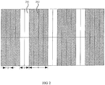
- Embodiments of the disclosure provide a mask. As shown in FIG. 2 , the mask comprises: a shielding region 202 and an opening region 201 which are alternately arranged. A width s of the opening region 201 is twice of a width p of one sub pixel, and a width w of the shielding region 202 between two adjacent opening regions 201 is four times of the width p of one sub pixel.
- the width s of the opening region 201 is twice of the width p of one sub pixel, namely, the opening region 201 exposes two sub pixels; and the width w of the shielding region 202 between two adjacent opening regions 201 is four times of the width p of one sub pixel, namely, the shielding region 202 shields four sub pixels.
- the width p of the sub pixel formed by the mask in the embodiments is half of the width of the sub pixel formed by the mask in the prior art.
- the thickness d of the mask is in direct proportion to the manufacturing difficulty of the mask.
- the embodiments realize that the width p of the sub pixel is reduced while the manufacturing difficulty of the mask is not increased; accordingly, the limitation of the thickness d of the mask on the width p of the sub pixel is greatly reduced, the PPI of the display device is increased, and the delicate degree of the image displayed by the display device is greatly improved.
- the available greatest thickness of the mask is the height of an isosceles triangle taking the width of the bottom of the shielding region 202 as a bottom side length and taking the side wall inclined angle ⁇ of the shielding region 202 as a base angle; in this case, if the PPI of the manufactured display device is kept unchanged (namely, the width p of each sub pixel is kept unchanged) compared with the mask in the prior art, the width of the shielding region 202 of the mask in the embodiments is increased by one time compared with the width of the mask in the prior art.
- the embodiments realize that the pixels are manufactured with a thicker mask in the case that the PPI is not reduced. The thicker the mask is, the harder the mask is to deform, and the lower the manufacturing difficulty of the mask is, so the manufacturing difficulty of the mask is reduced by the embodiments.
- the widths of the opening region 201 and the shielding region 202 may be properly increased so that the width of the formed sub pixel is smaller than the available smallest width in the prior art; on this basis, as the widths of the opening region 201 and the shielding region 202 are increased, the mask can be made thicker.
- the trade-off relation between the thickness d of the mask and the width p of the sub pixels is adjusted by adjusting the widths of the opening region 201 and the shielding region 202 and the thickness d of the mask, so the thickness d of the mask and the width p of the sub pixel achieve an optimal balance point according to practical requirements, which not only improves the PPI but also reduces the manufacturing difficulty of the mask.
- the structures of the masks for forming the sub pixels of different colors are different from each other, that is, the positions of the opening region and the shielding region of masks are different.
- factors for determining the positions of the opening region and the shielding region are an initial region (if all regions comprising the opening region and the shielding region are arranged from left to right, a first arranged region is the initial region and the initial region is a region positioned at the leftmost side of the mask) and a width of the initial region.
- the leftmost region in the mask (namely, the initial region of the mask) may be the shielding region 202 or the opening region 201, the leftmost regions of the masks for forming the sub pixels of different colors are different, the width of the leftmost region in the mask may be one, two, three or four times of the width p of one sub pixel, so as to enable the mask to meet the manufacturing demands of the sub pixels of different colors.
- the embodiments provide a mask group for manufacturing a first sub pixel, a second sub pixel and a third sub pixel of different colors.
- the mask group comprises: a first mask, a second mask and a third mask.
- the first mask is configured for manufacturing the first sub pixel
- the first mask is the mask described above
- the width s of an opening region 3011 is twice of the width p of one sub pixel
- the width w of a shielding region 3012 between two adjacent opening regions 3011 is four times of the width p of one sub pixel.
- the second mask is configured for manufacturing the second sub pixel
- the second mask is the mask described above
- the width s of an opening region 3021 is twice of the width p of one sub pixel
- the width w of a shielding region 3022 between two adjacent opening regions 3021 is four times of the width p of one sub pixel; in the case that the second mask and the first mask are completely overlapped with each other, a vertical projection of the opening region 3021 of the second mask on the first mask and the opening region 3011 of the first mask are alternately distributed, and a distance between the vertical projection of the opening region 3021 of the second mask on the first mask and the opening region 3011 of the first mask, which is adjacent to the vertical projection of the opening region 3021 of the second mask on the first mask, is the width p of one sub pixel.
- the third mask is configured for manufacturing the third sub pixel
- the third mask comprises an opening region 3031 and a shielding region 3032 which are alternately arranged, a width of the opening region 3031 is the width p of one sub pixel, and the width w of the shielding region 3032 between two adjacent opening regions 3031 of the third mask is twice of the width p of one sub pixel; in the case that the first mask, the second mask and the third mask are completely overlapped with one another, the vertical projection of the opening region 3021 of the second mask on the first mask and the vertical projection of the opening region of the third mask on the first mask are completely overlapped with the shielding region between two adjacent opening regions of the first mask.
- the masks for manufacturing the sub pixels of two colors adopt the structure of the mask according to the embodiments of the disclosure
- the mask for manufacturing the sub pixel of the remaining one color namely, the third mask
- the opening regions of the three masks are staggered without overlapping after the three masks are completely overlapped, so the pixel structure satisfying the practical needs can be manufactured on different positions of the display plane of the display device.
- the first mask and the second mask which are adopted in the mask group have the structure that two sub pixels are exposed by one opening region and four sub pixels are shielded by one shielding region, namely, in one manufacturing process, two sub pixels with the same color can be manufactured at the same time.
- the widths of the opening regions of the first and second masks are equal to the width of the opening region of the mask in the prior art, the width of the sub pixels manufactured by the mask group is half that of the prior art, so the PPI of the display device is improved; if the widths of the opening regions of the first and second masks are larger than that of the opening region of the mask in the prior art but smaller than twice of the width of the opening region of the mask in the prior art, the width of the sub pixels manufactured by the mask group is reduced, and the thicknesses of the masks can be properly increased, so the mask group can not only improve the PPI but also reduce the manufacturing difficulty of the masks; if the widths of the opening regions of the first and second masks is twice that of the opening region of the mask in the prior art, the first and second masks in the mask group can be made thicker, so the manufacturing difficulty of the first and second masks is reduced.
- the leftmost region in the first mask is the shielding region and the width of the leftmost region in the first mask is four times of the width p of one sub pixel;
- the leftmost region in the second mask is the shielding region, and the width of the leftmost region in the second mask is the width p of one sub pixel;
- the leftmost region in the third mask is the opening region, and the width of the leftmost region in the third mask is the width p of one sub pixel.
- arrangement of the sub pixels in each line from left to right in the finally obtained pixel structure is: the third sub pixel, the second sub pixel, the second sub pixel, the third sub pixel, the first sub pixel, the first sub pixel, the third sub pixel, the second sub pixel, the second sub pixel, the third sub pixel, the first sub pixel, the first sub pixel, the third sub pixel, the second sub pixel..., it is thus clear that the sub pixels in each line takes the first sub pixel, the third sub pixel, the second sub pixel, the second sub pixel, the third sub pixel and the first sub pixel as a repetition unit; and the pixel formed by the first sub pixel, the third sub pixel and the second sub pixel and the pixel formed by the second sub pixel, the third sub pixel and the first sub pixel are alternately arranged.
- the first sub pixel manufactured by the first mask is a red sub pixel
- the second sub pixel manufactured by the second mask is a blue sub pixel
- the third sub pixel manufactured by the third mask is a green sub pixel, so that each pixel comprises all colors needed by the full-color display of the display device.
- the colors of the sub pixels manufactured by the three masks contained in the mask group are not limited thereto.
- the embodiments of the disclosure provide a manufacturing method of pixels, the manufacturing method adopts the abovementioned mask group, and the manufacturing method comprises: manufacturing the first sub pixel by using the first mask in the mask group; manufacturing the second sub pixel by using the second mask in the mask group; and manufacturing the third sub pixel by using the third first mask in the mask group.
- the first and second masks adopted by the method has the advantages of improving the PPI and reducing the manufacturing difficulty of the masks, the PPI of the display device and the manufacturing difficulty of the masks can be reduced by adopting the manufacturing method of pixels.
- the processes for manufacturing the first, second and third sub pixels respectively adopt an evaporation process.
- the manufacturing the first sub pixel, the manufacturing the second sub pixel and the manufacturing the third sub pixels may be performed in no specific order, and the specific order may, preferably, be adjusted according to practical requirements.
- the first sub pixel is a red sub pixel
- the second sub pixel is a blue sub pixel
- the third sub pixel is a green sub pixel.
- the embodiments of the disclosure further provide a pixel structure which is manufactured by using the above manufacturing method.
- the pixel structure comprises a plurality of pixel repetition units 401, and each pixel repetition unit 401 comprises six sub pixels of the first sub pixel, the third sub pixel, the second sub pixel, the second sub pixel, the third sub pixel and the first sub pixel which are arranged sequentially.
- Each pixel repetition unit 401 comprises two pixels, and in each line of the sub pixels, the pixel formed of the first sub pixel, the third sub pixel and the second sub pixel and the pixel formed of the second sub pixel, the third sub pixel and the first sub pixel are alternately arranged.
- the arrangement of the sub pixels in each line is as shown in FIG. 4 .
- the width of each sub pixel of the pixel structure is reduced compared with that of the prior art, and the PPI is improved; and as the manufacturing difficulty of the adopted mask group is reduced, the manufacturing cost of the adopted mask group is reduced, so that the production cost of the pixel structure is reduced.
Landscapes
- Engineering & Computer Science (AREA)
- Chemical & Material Sciences (AREA)
- Manufacturing & Machinery (AREA)
- Chemical Kinetics & Catalysis (AREA)
- Materials Engineering (AREA)
- Mechanical Engineering (AREA)
- Metallurgy (AREA)
- Organic Chemistry (AREA)
- Physics & Mathematics (AREA)
- General Physics & Mathematics (AREA)
- Electroluminescent Light Sources (AREA)
Abstract
Description
- Embodiments of the disclosure relate to a mask, a mask group, a manufacturing method of pixels and a pixel structure.
- Generally, one pixel of an Organic Light-Emitting Diode (OLED) display device comprises sub pixels of three colors of Red (R), Green (G) and Blue (B). Pixels Per Inch (PPI) determines the delicate degree of an image displayed by the display device. The higher the PPI is, the more delicate the image is. The key to increase the PPI is how to reduce the size of a single sub pixel.
- At present, pixels of the OLED display device are formed by a vacuum evaporation process with a Fine Metal Mask (FMM). In the forming process, regions where the sub pixels of two colors are to be formed are shielded by the mask whereas a region where the sub pixel of the remaining one color is to be formed is exposed, so as to form the sub pixel of the remaining one color by evaporation. As shown in
FIG. 1 , an upper part of the diagram illustrates a plane view of a mask, and a lower part of the diagram illustrates a sectional view of the mask; the mask comprises ashielding region 101 and anopening region 102, and a side wall of theshielding region 101 has a certain side wall inclined angle θ. The smaller the side wall inclined angle 0 is, the larger an opening on the top of theopening region 102 is, then particles more easily get to an edge at the bottom of theopening region 102, and the size and shape of the evaporated sub pixel are closer to ideal size and shape. That is, the size of the side wall inclined angle θ determines the quality of the evaporation effect. At present, the side wall inclined angle θ is generally 40°-60°. - If d denotes a thickness of the mask, w denotes a width of the
shielding region 101, and s denotes a width of theopening region 102, then a width of one sub pixel is p=s=0.5w. If a is a width of a vertical projection of the side wall of theshielding region 101 on the bottom of theshielding region 101, and b is a width of a vertical projection of the top portion of theshielding region 101 on the bottom of theshielding region 101, then the width of theshielding region 101 is w=2a+b. Therefore, the width of one sub pixel is p=0.5(2a+b)=a+0.5b=(d/tan θ)+0.5b. It is thus clear that in a case where θ is given, the width of the sub pixel is limited to the thickness d of the mask; the thinner the mask is, the smaller the sub pixels is, and the larger the PPI is. - However, the thinner the mask is, the more difficult the manufacturing process of the mask is, and the higher the manufacturing cost of the mask is. At present, the thickness of the mask used for forming the pixels of the OLED by evaporation is usually 40µm, and the smallest is 30µm. However, even the mask with the smallest thickness of 30µm is adopted, the PPI of the OLED is still not greatly improved, which results in that the delicate degree of the image of the OLED display device cannot be further improved.
- Embodiments according to the disclosure provide a mask. The mask comprises a shielding region and an opening region which are alternately arranged. A width of the opening region is twice of a width of one sub pixel, and a width of the shielding region between two adjacent opening regions is four times of the width of one sub pixel.
- For example, a leftmost region in the mask is the shielding region or the opening region.
- For example, a width of the leftmost region in the mask is one, two, three or four times of the width of one sub pixel.
- For example, the leftmost regions of the masks for forming sub pixels of different colors are different.
- The embodiments according to the disclosure provide a mask group, for manufacturing a first sub pixel, a second sub pixel and a third sub pixel of different colors. The mask group comprises: a first mask, a second mask and a third mask. The first mask is configured for manufacturing the first sub pixel, and the first mask is the mask as described above. The second mask is configured for manufacturing the second sub pixel, and the second mask is the mask as described above. In the case that the second mask and the first mask are completely overlapped with each other, a vertical projection of the opening region of the second mask on the first mask and the opening region of the first mask are alternately distributed, and a distance between the vertical projection of the opening region of the second mask on the first mask and the opening region of the first mask, which is adjacent to the vertical projection of the opening region of the second mask on the first mask, is the width of one sub pixel. The third mask is configured for manufacturing the third sub pixel. The third mask comprises an opening region and a shielding region which are alternately arranged, a width of the opening region is the width of one sub pixel, and the width of the shielding region between two adjacent opening regions of the third mask is twice of the width of one sub pixel. In the case that the first mask, the second mask and the third mask are completely overlapped with one another, the vertical projection of the opening region of the second mask on the first mask and a vertical projection of the opening region of the third mask on the first mask are completely overlapped with the shielding region between two adjacent opening regions of the first mask.
- For example, a leftmost region in the first mask is the shielding region, and a width of the leftmost region in the first mask is four times of the width of one sub pixel.
- For example, the first sub pixel manufactured by the first mask is a red sub pixel.
- For example, a leftmost region in the second mask is the shielding region, and a width of the leftmost region in the second mask is the width of one sub pixel.
- For example, the second sub pixel manufactured by the second mask is a blue sub pixel.
- For example, a leftmost region in the third mask is the opening region, and a width of the leftmost region in the third mask is the width of one sub pixel.
- For example, the third sub pixel manufactured by the third mask is a green sub pixel.
- The embodiments according to the disclosure provide a manufacturing method of pixels. The manufacturing method adopts the mask group as described above. The manufacturing method comprises: manufacturing the first sub pixel by using the first mask in the mask group; manufacturing the second sub pixel by using the second mask in the mask group; and manufacturing the third sub pixel by using the third mask in the mask group.
- For example, the first sub pixel is a red sub pixel, the second sub pixel is a blue sub pixel, and the third sub pixel is a green sub pixel.
- For example, the manufacturing the first sub pixel, the manufacturing the second sub pixel and the manufacturing the third sub pixel are performed in no specific order.
- The embodiments according to the disclosure provide a pixel structure, and the pixel structure is manufactured by using the manufacturing method as described above.
- For example, the pixel structure comprises a plurality of pixel repetition units, and each pixel repetition unit comprises six sub pixels of the first sub pixel, the third sub pixel, the second sub pixel, the second sub pixel, the third sub pixel and the first sub pixel which are arranged sequentially.
- For example, the first sub pixel is a red sub pixel, the second sub pixel is a blue sub pixel, and the third sub pixel is a green sub pixel.
- In order to clearly illustrate the technical solution of the embodiments of the disclosure, the drawings of the embodiments will be briefly described in the following; it is obvious that the described drawings are only related to some embodiments of the disclosure and thus are not limitative of the disclosure.
-
FIG. 1 is a plane structural diagram and a cross-sectional structural diagram illustrating a mask in the prior art; -
FIG. 2 is a plane structural diagram illustrating a mask according to embodiments of the disclosure; -
FIG. 3(a) is a plane structural diagram illustrating a first mask of a mask group according to the embodiments of the disclosure; -
FIG. 3(b) is a plane structural diagram illustrating a second mask of the mask group according to the embodiments of the disclosure; -
FIG. 3(c) is a plane structural diagram illustrating a third mask of the mask group according to the embodiments of the disclosure; and -
FIG. 4 is a plane diagram illustrating a pixel structure according to the embodiments of the disclosure. - In order to make objects, technical details and advantages of the embodiments of the disclosure apparent, the technical solutions of the embodiment will be described in a clearly and fully understandable way in connection with the drawings related to the embodiments of the disclosure. It is obvious that the described embodiments are just a part but not all of the embodiments of the disclosure. Based on the described embodiments herein, those skilled in the art can obtain other embodiment(s), without any inventive work, which should be within the scope of the disclosure.
- Embodiments of the disclosure provide a mask. As shown in
FIG. 2 , the mask comprises: ashielding region 202 and anopening region 201 which are alternately arranged. A width s of theopening region 201 is twice of a width p of one sub pixel, and a width w of theshielding region 202 between two adjacentopening regions 201 is four times of the width p of one sub pixel. - In the mask, the width s of the
opening region 201 is twice of the width p of one sub pixel, namely, theopening region 201 exposes two sub pixels; and the width w of theshielding region 202 between two adjacentopening regions 201 is four times of the width p of one sub pixel, namely, theshielding region 202 shields four sub pixels. In this case, if the widths of theopening region 201 and the shieldingregion 202 and the thickness d of the mask are kept unchanged compared with those of the mask in the prior art, the width p of the sub pixel formed by the mask in the embodiments is half of the width of the sub pixel formed by the mask in the prior art. The thickness d of the mask is in direct proportion to the manufacturing difficulty of the mask. The embodiments realize that the width p of the sub pixel is reduced while the manufacturing difficulty of the mask is not increased; accordingly, the limitation of the thickness d of the mask on the width p of the sub pixel is greatly reduced, the PPI of the display device is increased, and the delicate degree of the image displayed by the display device is greatly improved. - On the other hand, the available greatest thickness of the mask is the height of an isosceles triangle taking the width of the bottom of the shielding
region 202 as a bottom side length and taking the side wall inclined angle θ of the shieldingregion 202 as a base angle; in this case, if the PPI of the manufactured display device is kept unchanged (namely, the width p of each sub pixel is kept unchanged) compared with the mask in the prior art, the width of the shieldingregion 202 of the mask in the embodiments is increased by one time compared with the width of the mask in the prior art. Furthermore, if the side wall inclined angle θ of the shielding region is kept unchanged compared with the mask in the prior art, it is apparent that the available greatest thickness of the mask in the embodiments is much larger than that of the mask in the prior art. That is to say, the embodiments realize that the pixels are manufactured with a thicker mask in the case that the PPI is not reduced. The thicker the mask is, the harder the mask is to deform, and the lower the manufacturing difficulty of the mask is, so the manufacturing difficulty of the mask is reduced by the embodiments. - Known from above analysis, a trade-off relationship exists between the thickness d of the mask and the width p of the sub pixel. In practical design and manufacture processes, it is unnecessary to keep the widths of the
opening region 201 and the shieldingregion 202 and the thickness d of the mask unchanged to improve the PPI or it is unnecessary to keep the PPI unchanged to reduce the manufacturing difficulty of the mask. Based on the embodiments of the disclosure, the widths of theopening region 201 and the shieldingregion 202 may be properly increased so that the width of the formed sub pixel is smaller than the available smallest width in the prior art; on this basis, as the widths of theopening region 201 and the shieldingregion 202 are increased, the mask can be made thicker. It is thus clear that by adopting the mask according to the embodiments, the trade-off relation between the thickness d of the mask and the width p of the sub pixels is adjusted by adjusting the widths of theopening region 201 and the shieldingregion 202 and the thickness d of the mask, so the thickness d of the mask and the width p of the sub pixel achieve an optimal balance point according to practical requirements, which not only improves the PPI but also reduces the manufacturing difficulty of the mask. - As the sub pixels of different colors are distributed on different positons of a display plane of the display device, the structures of the masks for forming the sub pixels of different colors are different from each other, that is, the positions of the opening region and the shielding region of masks are different. As the opening region and the shielding region of the mask are alternately arranged, factors for determining the positions of the opening region and the shielding region are an initial region (if all regions comprising the opening region and the shielding region are arranged from left to right, a first arranged region is the initial region and the initial region is a region positioned at the leftmost side of the mask) and a width of the initial region. Particularly, the leftmost region in the mask (namely, the initial region of the mask) may be the shielding
region 202 or theopening region 201, the leftmost regions of the masks for forming the sub pixels of different colors are different, the width of the leftmost region in the mask may be one, two, three or four times of the width p of one sub pixel, so as to enable the mask to meet the manufacturing demands of the sub pixels of different colors. - Based on the mask with above structure, the embodiments provide a mask group for manufacturing a first sub pixel, a second sub pixel and a third sub pixel of different colors. The mask group comprises: a first mask, a second mask and a third mask.
- As shown in
FIG. 3(a) , the first mask is configured for manufacturing the first sub pixel, the first mask is the mask described above, the width s of anopening region 3011 is twice of the width p of one sub pixel, and the width w of ashielding region 3012 between twoadjacent opening regions 3011 is four times of the width p of one sub pixel. - As shown in
FIG. 3(b) , the second mask is configured for manufacturing the second sub pixel, the second mask is the mask described above, the width s of anopening region 3021 is twice of the width p of one sub pixel, and the width w of ashielding region 3022 between twoadjacent opening regions 3021 is four times of the width p of one sub pixel; in the case that the second mask and the first mask are completely overlapped with each other, a vertical projection of theopening region 3021 of the second mask on the first mask and theopening region 3011 of the first mask are alternately distributed, and a distance between the vertical projection of theopening region 3021 of the second mask on the first mask and theopening region 3011 of the first mask, which is adjacent to the vertical projection of theopening region 3021 of the second mask on the first mask, is the width p of one sub pixel. - As shown in
FIG. 3(c) , the third mask is configured for manufacturing the third sub pixel, the third mask comprises anopening region 3031 and ashielding region 3032 which are alternately arranged, a width of theopening region 3031 is the width p of one sub pixel, and the width w of theshielding region 3032 between twoadjacent opening regions 3031 of the third mask is twice of the width p of one sub pixel; in the case that the first mask, the second mask and the third mask are completely overlapped with one another, the vertical projection of theopening region 3021 of the second mask on the first mask and the vertical projection of the opening region of the third mask on the first mask are completely overlapped with the shielding region between two adjacent opening regions of the first mask. - The masks for manufacturing the sub pixels of two colors (namely, the first mask and the second mask) adopt the structure of the mask according to the embodiments of the disclosure, the mask for manufacturing the sub pixel of the remaining one color (namely, the third mask) adopts the structure of a conventional mask in the prior art, and the opening regions of the three masks are staggered without overlapping after the three masks are completely overlapped, so the pixel structure satisfying the practical needs can be manufactured on different positions of the display plane of the display device.
- As the first mask and the second mask which are adopted in the mask group have the structure that two sub pixels are exposed by one opening region and four sub pixels are shielded by one shielding region, namely, in one manufacturing process, two sub pixels with the same color can be manufactured at the same time. Compared with the mask in the prior art, if the widths of the opening regions of the first and second masks are equal to the width of the opening region of the mask in the prior art, the width of the sub pixels manufactured by the mask group is half that of the prior art, so the PPI of the display device is improved; if the widths of the opening regions of the first and second masks are larger than that of the opening region of the mask in the prior art but smaller than twice of the width of the opening region of the mask in the prior art, the width of the sub pixels manufactured by the mask group is reduced, and the thicknesses of the masks can be properly increased, so the mask group can not only improve the PPI but also reduce the manufacturing difficulty of the masks; if the widths of the opening regions of the first and second masks is twice that of the opening region of the mask in the prior art, the first and second masks in the mask group can be made thicker, so the manufacturing difficulty of the first and second masks is reduced.
- For example, the leftmost region in the first mask is the shielding region and the width of the leftmost region in the first mask is four times of the width p of one sub pixel; the leftmost region in the second mask is the shielding region, and the width of the leftmost region in the second mask is the width p of one sub pixel; the leftmost region in the third mask is the opening region, and the width of the leftmost region in the third mask is the width p of one sub pixel. Therefore, arrangement of the sub pixels in each line from left to right in the finally obtained pixel structure is: the third sub pixel, the second sub pixel, the second sub pixel, the third sub pixel, the first sub pixel, the first sub pixel, the third sub pixel, the second sub pixel, the second sub pixel, the third sub pixel, the first sub pixel, the first sub pixel, the third sub pixel, the second sub pixel..., it is thus clear that the sub pixels in each line takes the first sub pixel, the third sub pixel, the second sub pixel, the second sub pixel, the third sub pixel and the first sub pixel as a repetition unit; and the pixel formed by the first sub pixel, the third sub pixel and the second sub pixel and the pixel formed by the second sub pixel, the third sub pixel and the first sub pixel are alternately arranged.
- For example, the first sub pixel manufactured by the first mask is a red sub pixel, the second sub pixel manufactured by the second mask is a blue sub pixel, and the third sub pixel manufactured by the third mask is a green sub pixel, so that each pixel comprises all colors needed by the full-color display of the display device. However, the colors of the sub pixels manufactured by the three masks contained in the mask group are not limited thereto.
- The embodiments of the disclosure provide a manufacturing method of pixels, the manufacturing method adopts the abovementioned mask group, and the manufacturing method comprises: manufacturing the first sub pixel by using the first mask in the mask group; manufacturing the second sub pixel by using the second mask in the mask group; and manufacturing the third sub pixel by using the third first mask in the mask group.
- As the first and second masks adopted by the method has the advantages of improving the PPI and reducing the manufacturing difficulty of the masks, the PPI of the display device and the manufacturing difficulty of the masks can be reduced by adopting the manufacturing method of pixels.
- For example, the processes for manufacturing the first, second and third sub pixels respectively adopt an evaporation process.
- The manufacturing the first sub pixel, the manufacturing the second sub pixel and the manufacturing the third sub pixels may be performed in no specific order, and the specific order may, preferably, be adjusted according to practical requirements.
- For example, the first sub pixel is a red sub pixel, the second sub pixel is a blue sub pixel, and the third sub pixel is a green sub pixel.
- The embodiments of the disclosure further provide a pixel structure which is manufactured by using the above manufacturing method. As shown in
FIG. 4 , the pixel structure comprises a plurality ofpixel repetition units 401, and eachpixel repetition unit 401 comprises six sub pixels of the first sub pixel, the third sub pixel, the second sub pixel, the second sub pixel, the third sub pixel and the first sub pixel which are arranged sequentially. Eachpixel repetition unit 401 comprises two pixels, and in each line of the sub pixels, the pixel formed of the first sub pixel, the third sub pixel and the second sub pixel and the pixel formed of the second sub pixel, the third sub pixel and the first sub pixel are alternately arranged. - If the first sub pixel is a red sub pixel, the second sub pixel is a blue sub pixel and the third sub pixel is a green sub pixel, the arrangement of the sub pixels in each line is as shown in
FIG. 4 . - As the mask group is adopted to form the pixel structure, the width of each sub pixel of the pixel structure is reduced compared with that of the prior art, and the PPI is improved; and as the manufacturing difficulty of the adopted mask group is reduced, the manufacturing cost of the adopted mask group is reduced, so that the production cost of the pixel structure is reduced.
- The foregoing embodiments merely are exemplary embodiments of the disclosure, and not intended to define the scope of the disclosure, and the scope of the disclosure is determined by the appended claims.
- The present application claims priority of
Chinese Patent Application No. 201410421343.5 filed on August 25, 2014
Claims (17)
- A mask, comprising a shielding region and an opening region which are alternately arranged, wherein
a width of the opening region is twice of a width of one sub pixel, and a width of the shielding region between two adjacent opening regions is four times of the width of one sub pixel. - The mask according to claim 1, wherein a leftmost region in the mask is the shielding region or the opening region.
- The mask according to claim 2, wherein a width of the leftmost region in the mask is one, two, three or four times of the width of one sub pixel.
- The mask according to claim 2, wherein the leftmost regions of the masks for forming sub pixels of different colors are different.
- A mask group, for manufacturing a first sub pixel, a second sub pixel and a third sub pixel of different colors, and comprising:a first mask configured for manufacturing the first sub pixel, the first mask being the mask in any one of claims 1-4;a second mask configured for manufacturing the second sub pixel, the second mask being the mask in any one of claims 1-4, wherein in the case that the second mask and the first mask are completely overlapped with each other, a vertical projection of the opening region of the second mask on the first mask and the opening region of the first mask are alternately distributed, and a distance between the vertical projection of the opening region of the second mask on the first mask and the opening region of the first mask, which is adjacent to the vertical projection of the opening region of the second mask on the first mask, is the width of one sub pixel;a third mask configured for manufacturing the third sub pixel, wherein the third mask comprises an opening region and a shielding region which are alternately arranged, a width of the opening region is the width of one sub pixel, and the width of the shielding region between two adjacent opening regions of the third mask is twice of the width of one sub pixel; in the case that the first mask, the second mask and the third mask are completely overlapped with one another, the vertical projection of the opening region of the second mask on the first mask and a vertical projection of the opening region of the third mask on the first mask are completely overlapped with the shielding region between two adjacent opening regions of the first mask..
- The mask group according to claim 5, wherein a leftmost region in the first mask is the shielding region, and a width of the leftmost region in the first mask is four times of the width of one sub pixel.
- The mask group according to claim 6, wherein the first sub pixel manufactured by the first mask is a red sub pixel.
- The mask group according to claim 5, wherein a leftmost region in the second mask is the shielding region, and a width of the leftmost region in the second mask is the width of one sub pixel.
- The mask group according to claim 8, wherein the second sub pixel manufactured by the second mask is a blue sub pixel.
- The mask group according to claim 5, wherein a leftmost region in the third mask is the opening region, and a width of the leftmost region in the third mask is the width of one sub pixel.
- The mask group according to claim 10, wherein the third sub pixel manufactured by the third mask is a green sub pixel.
- A manufacturing method of pixels, wherein
the manufacturing method adopts the mask group in any one of claims 5-11; and
the manufacturing method comprises: manufacturing the first sub pixel by using the first mask in the mask group; manufacturing the second sub pixel by using the second mask in the mask group; and manufacturing the third sub pixel by using the third mask in the mask group. - The manufacturing method according to claim 12, wherein the first sub pixel is a red sub pixel, the second sub pixel is a blue sub pixel, and the third sub pixel is a green sub pixel.
- The manufacturing method according to claim 12, wherein the manufacturing the first sub pixel, the manufacturing the second sub pixel and the manufacturing the third sub pixel are performed in no specific order.
- A pixel structure, manufactured by using the manufacturing method in any one of claims 12-14.
- The pixel structure according to claim 15, wherein the pixel structure comprises a plurality of pixel repetition units, and each pixel repetition unit comprises six sub pixels of the first sub pixel, the third sub pixel, the second sub pixel, the second sub pixel, the third sub pixel and the first sub pixel which are arranged sequentially.
- The pixel structure according to claim 16, wherein the first sub pixel is a red sub pixel, the second sub pixel is a blue sub pixel, and the third sub pixel is a green sub pixel.
Applications Claiming Priority (2)
| Application Number | Priority Date | Filing Date | Title |
|---|---|---|---|
| CN201410421343.5A CN104330954B (en) | 2014-08-25 | 2014-08-25 | The making method of mask, mask group, pixel and pixel structure |
| PCT/CN2014/095285 WO2016029610A1 (en) | 2014-08-25 | 2014-12-29 | Mask plate, mask plate assembly, method for manufacturing pixel and pixel structure |
Publications (3)
| Publication Number | Publication Date |
|---|---|
| EP3187937A1 true EP3187937A1 (en) | 2017-07-05 |
| EP3187937A4 EP3187937A4 (en) | 2018-06-20 |
| EP3187937B1 EP3187937B1 (en) | 2021-03-03 |
Family
ID=52405706
Family Applications (1)
| Application Number | Title | Priority Date | Filing Date |
|---|---|---|---|
| EP14863039.5A Active EP3187937B1 (en) | 2014-08-25 | 2014-12-29 | Mask plate, mask plate assembly and use of mask plate assembly for pixel manufacturing |
Country Status (4)
| Country | Link |
|---|---|
| US (1) | US9349922B2 (en) |
| EP (1) | EP3187937B1 (en) |
| CN (1) | CN104330954B (en) |
| WO (1) | WO2016029610A1 (en) |
Families Citing this family (9)
| Publication number | Priority date | Publication date | Assignee | Title |
|---|---|---|---|---|
| CN106676468A (en) * | 2015-11-10 | 2017-05-17 | 上海和辉光电有限公司 | Covering sheet, evaporation cover, evaporation covering device and evaporation process |
| CN105552104A (en) * | 2016-01-05 | 2016-05-04 | 京东方科技集团股份有限公司 | Organic light emitting diode (OLED) pixel array, method for fabricating OLED pixel array, OLED display panel and display device |
| CN107359283B (en) * | 2017-07-18 | 2019-03-29 | 广州新视界光电科技有限公司 | Preparation method, array substrate, display panel and the display device of array substrate |
| CN107604314B (en) * | 2017-09-18 | 2019-10-29 | 联想(北京)有限公司 | A kind of evaporation coating method and deposition system |
| CN108642440B (en) * | 2018-05-14 | 2019-09-17 | 昆山国显光电有限公司 | Mask plate and mask assembly |
| CN112216219A (en) * | 2019-07-09 | 2021-01-12 | 成都辰显光电有限公司 | Pixel arrangement structure, display panel and display device |
| CN110931639A (en) * | 2019-11-26 | 2020-03-27 | 武汉华星光电半导体显示技术有限公司 | Pixel arrangement display equipment capable of improving pixel resolution and evaporation method |
| US11659759B2 (en) * | 2021-01-06 | 2023-05-23 | Applied Materials, Inc. | Method of making high resolution OLED fabricated with overlapped masks |
| CN118039754B (en) * | 2024-04-12 | 2024-06-07 | 江西兆驰半导体有限公司 | Preparation method of flip mini light-emitting diode chip |
Family Cites Families (26)
| Publication number | Priority date | Publication date | Assignee | Title |
|---|---|---|---|---|
| JP2000112114A (en) * | 1998-10-08 | 2000-04-21 | Hitachi Ltd | Semiconductor device and method of manufacturing semiconductor device |
| US6534425B1 (en) * | 1999-12-02 | 2003-03-18 | Seagate Technology Llc | Mask design and method for controlled profile fabrication |
| JP2002072980A (en) * | 2000-08-31 | 2002-03-12 | Nec Corp | Color video display method and device |
| SG126714A1 (en) * | 2002-01-24 | 2006-11-29 | Semiconductor Energy Lab | Light emitting device and method of manufacturing the same |
| JP2004311319A (en) * | 2003-04-10 | 2004-11-04 | Sony Corp | Film forming mask apparatus and method of manufacturing thin film device using the same |
| US6919681B2 (en) * | 2003-04-30 | 2005-07-19 | Eastman Kodak Company | Color OLED display with improved power efficiency |
| US8665247B2 (en) * | 2003-05-30 | 2014-03-04 | Global Oled Technology Llc | Flexible display |
| US7532225B2 (en) * | 2003-09-18 | 2009-05-12 | Kabushiki Kaisha Toshiba | Three-dimensional image display device |
| KR100997971B1 (en) * | 2003-11-19 | 2010-12-02 | 삼성전자주식회사 | Crystallization mask, crystallization method using same and manufacturing method of thin film transistor array panel including same |
| US7439667B2 (en) * | 2003-12-12 | 2008-10-21 | Semiconductor Energy Laboratory Co., Ltd. | Light emitting device with specific four color arrangement |
| JP2005276480A (en) * | 2004-03-23 | 2005-10-06 | Seiko Epson Corp | Mask, mask manufacturing method, thin film pattern forming method, electro-optical device manufacturing method, and electronic apparatus |
| JP4928073B2 (en) * | 2004-11-16 | 2012-05-09 | グローバル・オーエルイーディー・テクノロジー・リミテッド・ライアビリティ・カンパニー | Organic EL panel manufacturing method and organic EL panel |
| TWI268737B (en) * | 2005-07-29 | 2006-12-11 | Au Optronics Corp | Full-color organic electroluminescence panel with high resolution |
| US7914971B2 (en) * | 2005-08-12 | 2011-03-29 | Semiconductor Energy Laboratory Co., Ltd. | Light exposure mask and method for manufacturing semiconductor device using the same |
| TWI275052B (en) * | 2006-04-07 | 2007-03-01 | Ind Tech Res Inst | OLED pixel structure and method of manufacturing the same |
| KR101192798B1 (en) * | 2006-06-30 | 2012-10-18 | 엘지디스플레이 주식회사 | Shadow Mask and Method for Manufacturing Organic Emitting Light Device |
| JP5371240B2 (en) * | 2006-12-27 | 2013-12-18 | 株式会社半導体エネルギー研究所 | Wiring fabrication method |
| US9070323B2 (en) * | 2009-02-17 | 2015-06-30 | Global Oled Technology Llc | Chiplet display with multiple passive-matrix controllers |
| JP2010272300A (en) * | 2009-05-20 | 2010-12-02 | Canon Inc | Manufacturing method of organic EL display device |
| KR101156432B1 (en) * | 2009-12-15 | 2012-06-18 | 삼성모바일디스플레이주식회사 | Mask frame assembly for thin layer deposition and organic light emitting display device |
| TWI429326B (en) * | 2010-11-10 | 2014-03-01 | Au Optronics Corp | Light emitting device and manufacturing method thereof |
| WO2012124629A1 (en) * | 2011-03-15 | 2012-09-20 | シャープ株式会社 | Vapor deposition device, vapor deposition method, and method for producing organic el display device |
| KR20140095354A (en) * | 2013-01-24 | 2014-08-01 | 롬엔드하스전자재료코리아유한회사 | Organic electroluminescence device, and display device including the same |
| JPWO2014126033A1 (en) * | 2013-02-12 | 2017-02-02 | 富士フイルム株式会社 | Manufacturing method of cured film, cured film, liquid crystal display device, organic EL display device, and touch panel display device |
| CN103715227A (en) * | 2013-12-26 | 2014-04-09 | 京东方科技集团股份有限公司 | Display panel, driving method of display panel and display device |
| CN103854570B (en) | 2014-02-20 | 2016-08-17 | 北京京东方光电科技有限公司 | Display base plate and driving method thereof and display device |
-
2014
- 2014-08-25 CN CN201410421343.5A patent/CN104330954B/en active Active
- 2014-12-29 EP EP14863039.5A patent/EP3187937B1/en active Active
- 2014-12-29 US US14/646,915 patent/US9349922B2/en active Active
- 2014-12-29 WO PCT/CN2014/095285 patent/WO2016029610A1/en not_active Ceased
Also Published As
| Publication number | Publication date |
|---|---|
| CN104330954A (en) | 2015-02-04 |
| WO2016029610A1 (en) | 2016-03-03 |
| US9349922B2 (en) | 2016-05-24 |
| US20160056342A1 (en) | 2016-02-25 |
| CN104330954B (en) | 2016-06-01 |
| EP3187937B1 (en) | 2021-03-03 |
| EP3187937A4 (en) | 2018-06-20 |
Similar Documents
| Publication | Publication Date | Title |
|---|---|---|
| US9349922B2 (en) | Mask, mask group, manufacturing method of pixels and pixel structure | |
| EP3488469B1 (en) | Pixel arrangement structure, display substrate, display apparatus and method of fabrication thereof | |
| US10825870B2 (en) | Pixel structure and display device | |
| US11690269B2 (en) | Display substrate, manufacturing method thereof, and display apparatus | |
| CN105568217B (en) | Metal mask plate and preparation method thereof | |
| KR20200013782A (en) | Mask and Mask Assembly | |
| US11018197B2 (en) | Display panel and fabrication method thereof | |
| US20160260923A1 (en) | Organic light emitting diode display panel, manufacturing method thereof and mask plate | |
| US20180090545A1 (en) | Oled pixel array, method for preparing oled pixel array, oled display panel and display apparatus | |
| KR102090198B1 (en) | Fine Metal Mask and method of manufacturing the same | |
| CN104201192A (en) | Display pixel structure, metal mask and OLED display | |
| WO2019080871A1 (en) | Mask device and mask assembly thereof, and mask plate | |
| US20180374908A1 (en) | Display substrate and method for manufacturing the same, and display device | |
| US9673426B2 (en) | Mask plate for coating glass cement and coating method using the same | |
| WO2015165210A1 (en) | Metal mask plate | |
| CN110690259B (en) | An array substrate, an OLED display panel, and a mask | |
| WO2020107842A1 (en) | Pixel arrangement structure of display panel and display device | |
| US9905762B2 (en) | Display substrate and fabricating method thereof, and system for fabricating display substrate and display device | |
| US11489017B2 (en) | Display panel, method for preparing display panel, and display device | |
| JP2019514152A5 (en) | ||
| US20210335911A1 (en) | Organic light-emitting diode pixel structure and display device | |
| CN105529353A (en) | Display and pixel structure therefor | |
| TW201607019A (en) | Organic light-emitting diode display panel and the pixel arrangement structure of the display panel | |
| US9716245B2 (en) | Organic electroluminescent device and preparation method thereof, and display device | |
| JP2000068053A (en) | Manufacturing method of organic light emitting device |
Legal Events
| Date | Code | Title | Description |
|---|---|---|---|
| PUAI | Public reference made under article 153(3) epc to a published international application that has entered the european phase |
Free format text: ORIGINAL CODE: 0009012 |
|
| STAA | Information on the status of an ep patent application or granted ep patent |
Free format text: STATUS: REQUEST FOR EXAMINATION WAS MADE |
|
| 17P | Request for examination filed |
Effective date: 20150522 |
|
| AK | Designated contracting states |
Kind code of ref document: A1 Designated state(s): AL AT BE BG CH CY CZ DE DK EE ES FI FR GB GR HR HU IE IS IT LI LT LU LV MC MK MT NL NO PL PT RO RS SE SI SK SM TR |
|
| AX | Request for extension of the european patent |
Extension state: BA ME |
|
| DAX | Request for extension of the european patent (deleted) | ||
| A4 | Supplementary search report drawn up and despatched |
Effective date: 20180518 |
|
| RIC1 | Information provided on ipc code assigned before grant |
Ipc: H01L 51/56 20060101ALI20180514BHEP Ipc: H01L 21/77 20170101ALI20180514BHEP Ipc: H01L 27/32 20060101ALI20180514BHEP Ipc: G03F 1/44 20120101AFI20180514BHEP |
|
| STAA | Information on the status of an ep patent application or granted ep patent |
Free format text: STATUS: EXAMINATION IS IN PROGRESS |
|
| 17Q | First examination report despatched |
Effective date: 20200416 |
|
| GRAP | Despatch of communication of intention to grant a patent |
Free format text: ORIGINAL CODE: EPIDOSNIGR1 |
|
| STAA | Information on the status of an ep patent application or granted ep patent |
Free format text: STATUS: GRANT OF PATENT IS INTENDED |
|
| INTG | Intention to grant announced |
Effective date: 20200922 |
|
| GRAS | Grant fee paid |
Free format text: ORIGINAL CODE: EPIDOSNIGR3 |
|
| GRAA | (expected) grant |
Free format text: ORIGINAL CODE: 0009210 |
|
| STAA | Information on the status of an ep patent application or granted ep patent |
Free format text: STATUS: THE PATENT HAS BEEN GRANTED |
|
| AK | Designated contracting states |
Kind code of ref document: B1 Designated state(s): AL AT BE BG CH CY CZ DE DK EE ES FI FR GB GR HR HU IE IS IT LI LT LU LV MC MK MT NL NO PL PT RO RS SE SI SK SM TR |
|
| REG | Reference to a national code |
Ref country code: GB Ref legal event code: FG4D |
|
| REG | Reference to a national code |
Ref country code: AT Ref legal event code: REF Ref document number: 1367873 Country of ref document: AT Kind code of ref document: T Effective date: 20210315 Ref country code: CH Ref legal event code: EP |
|
| REG | Reference to a national code |
Ref country code: DE Ref legal event code: R096 Ref document number: 602014075442 Country of ref document: DE |
|
| REG | Reference to a national code |
Ref country code: IE Ref legal event code: FG4D |
|
| REG | Reference to a national code |
Ref country code: LT Ref legal event code: MG9D |
|
| PG25 | Lapsed in a contracting state [announced via postgrant information from national office to epo] |
Ref country code: NO Free format text: LAPSE BECAUSE OF FAILURE TO SUBMIT A TRANSLATION OF THE DESCRIPTION OR TO PAY THE FEE WITHIN THE PRESCRIBED TIME-LIMIT Effective date: 20210603 Ref country code: BG Free format text: LAPSE BECAUSE OF FAILURE TO SUBMIT A TRANSLATION OF THE DESCRIPTION OR TO PAY THE FEE WITHIN THE PRESCRIBED TIME-LIMIT Effective date: 20210603 Ref country code: GR Free format text: LAPSE BECAUSE OF FAILURE TO SUBMIT A TRANSLATION OF THE DESCRIPTION OR TO PAY THE FEE WITHIN THE PRESCRIBED TIME-LIMIT Effective date: 20210604 Ref country code: HR Free format text: LAPSE BECAUSE OF FAILURE TO SUBMIT A TRANSLATION OF THE DESCRIPTION OR TO PAY THE FEE WITHIN THE PRESCRIBED TIME-LIMIT Effective date: 20210303 Ref country code: FI Free format text: LAPSE BECAUSE OF FAILURE TO SUBMIT A TRANSLATION OF THE DESCRIPTION OR TO PAY THE FEE WITHIN THE PRESCRIBED TIME-LIMIT Effective date: 20210303 Ref country code: LT Free format text: LAPSE BECAUSE OF FAILURE TO SUBMIT A TRANSLATION OF THE DESCRIPTION OR TO PAY THE FEE WITHIN THE PRESCRIBED TIME-LIMIT Effective date: 20210303 |
|
| REG | Reference to a national code |
Ref country code: NL Ref legal event code: MP Effective date: 20210303 |
|
| REG | Reference to a national code |
Ref country code: AT Ref legal event code: MK05 Ref document number: 1367873 Country of ref document: AT Kind code of ref document: T Effective date: 20210303 |
|
| PG25 | Lapsed in a contracting state [announced via postgrant information from national office to epo] |
Ref country code: SE Free format text: LAPSE BECAUSE OF FAILURE TO SUBMIT A TRANSLATION OF THE DESCRIPTION OR TO PAY THE FEE WITHIN THE PRESCRIBED TIME-LIMIT Effective date: 20210303 Ref country code: PL Free format text: LAPSE BECAUSE OF FAILURE TO SUBMIT A TRANSLATION OF THE DESCRIPTION OR TO PAY THE FEE WITHIN THE PRESCRIBED TIME-LIMIT Effective date: 20210303 Ref country code: RS Free format text: LAPSE BECAUSE OF FAILURE TO SUBMIT A TRANSLATION OF THE DESCRIPTION OR TO PAY THE FEE WITHIN THE PRESCRIBED TIME-LIMIT Effective date: 20210303 Ref country code: LV Free format text: LAPSE BECAUSE OF FAILURE TO SUBMIT A TRANSLATION OF THE DESCRIPTION OR TO PAY THE FEE WITHIN THE PRESCRIBED TIME-LIMIT Effective date: 20210303 |
|
| PG25 | Lapsed in a contracting state [announced via postgrant information from national office to epo] |
Ref country code: NL Free format text: LAPSE BECAUSE OF FAILURE TO SUBMIT A TRANSLATION OF THE DESCRIPTION OR TO PAY THE FEE WITHIN THE PRESCRIBED TIME-LIMIT Effective date: 20210303 |
|
| PG25 | Lapsed in a contracting state [announced via postgrant information from national office to epo] |
Ref country code: SM Free format text: LAPSE BECAUSE OF FAILURE TO SUBMIT A TRANSLATION OF THE DESCRIPTION OR TO PAY THE FEE WITHIN THE PRESCRIBED TIME-LIMIT Effective date: 20210303 Ref country code: AT Free format text: LAPSE BECAUSE OF FAILURE TO SUBMIT A TRANSLATION OF THE DESCRIPTION OR TO PAY THE FEE WITHIN THE PRESCRIBED TIME-LIMIT Effective date: 20210303 Ref country code: EE Free format text: LAPSE BECAUSE OF FAILURE TO SUBMIT A TRANSLATION OF THE DESCRIPTION OR TO PAY THE FEE WITHIN THE PRESCRIBED TIME-LIMIT Effective date: 20210303 Ref country code: CZ Free format text: LAPSE BECAUSE OF FAILURE TO SUBMIT A TRANSLATION OF THE DESCRIPTION OR TO PAY THE FEE WITHIN THE PRESCRIBED TIME-LIMIT Effective date: 20210303 |
|
| PG25 | Lapsed in a contracting state [announced via postgrant information from national office to epo] |
Ref country code: IS Free format text: LAPSE BECAUSE OF FAILURE TO SUBMIT A TRANSLATION OF THE DESCRIPTION OR TO PAY THE FEE WITHIN THE PRESCRIBED TIME-LIMIT Effective date: 20210703 Ref country code: PT Free format text: LAPSE BECAUSE OF FAILURE TO SUBMIT A TRANSLATION OF THE DESCRIPTION OR TO PAY THE FEE WITHIN THE PRESCRIBED TIME-LIMIT Effective date: 20210705 Ref country code: SK Free format text: LAPSE BECAUSE OF FAILURE TO SUBMIT A TRANSLATION OF THE DESCRIPTION OR TO PAY THE FEE WITHIN THE PRESCRIBED TIME-LIMIT Effective date: 20210303 Ref country code: RO Free format text: LAPSE BECAUSE OF FAILURE TO SUBMIT A TRANSLATION OF THE DESCRIPTION OR TO PAY THE FEE WITHIN THE PRESCRIBED TIME-LIMIT Effective date: 20210303 |
|
| REG | Reference to a national code |
Ref country code: DE Ref legal event code: R097 Ref document number: 602014075442 Country of ref document: DE |
|
| PLBE | No opposition filed within time limit |
Free format text: ORIGINAL CODE: 0009261 |
|
| STAA | Information on the status of an ep patent application or granted ep patent |
Free format text: STATUS: NO OPPOSITION FILED WITHIN TIME LIMIT |
|
| PG25 | Lapsed in a contracting state [announced via postgrant information from national office to epo] |
Ref country code: AL Free format text: LAPSE BECAUSE OF FAILURE TO SUBMIT A TRANSLATION OF THE DESCRIPTION OR TO PAY THE FEE WITHIN THE PRESCRIBED TIME-LIMIT Effective date: 20210303 Ref country code: ES Free format text: LAPSE BECAUSE OF FAILURE TO SUBMIT A TRANSLATION OF THE DESCRIPTION OR TO PAY THE FEE WITHIN THE PRESCRIBED TIME-LIMIT Effective date: 20210303 Ref country code: DK Free format text: LAPSE BECAUSE OF FAILURE TO SUBMIT A TRANSLATION OF THE DESCRIPTION OR TO PAY THE FEE WITHIN THE PRESCRIBED TIME-LIMIT Effective date: 20210303 |
|
| 26N | No opposition filed |
Effective date: 20211206 |
|
| PG25 | Lapsed in a contracting state [announced via postgrant information from national office to epo] |
Ref country code: SI Free format text: LAPSE BECAUSE OF FAILURE TO SUBMIT A TRANSLATION OF THE DESCRIPTION OR TO PAY THE FEE WITHIN THE PRESCRIBED TIME-LIMIT Effective date: 20210303 |
|
| PG25 | Lapsed in a contracting state [announced via postgrant information from national office to epo] |
Ref country code: IT Free format text: LAPSE BECAUSE OF FAILURE TO SUBMIT A TRANSLATION OF THE DESCRIPTION OR TO PAY THE FEE WITHIN THE PRESCRIBED TIME-LIMIT Effective date: 20210303 |
|
| PG25 | Lapsed in a contracting state [announced via postgrant information from national office to epo] |
Ref country code: IS Free format text: LAPSE BECAUSE OF FAILURE TO SUBMIT A TRANSLATION OF THE DESCRIPTION OR TO PAY THE FEE WITHIN THE PRESCRIBED TIME-LIMIT Effective date: 20210703 |
|
| PG25 | Lapsed in a contracting state [announced via postgrant information from national office to epo] |
Ref country code: MC Free format text: LAPSE BECAUSE OF FAILURE TO SUBMIT A TRANSLATION OF THE DESCRIPTION OR TO PAY THE FEE WITHIN THE PRESCRIBED TIME-LIMIT Effective date: 20210303 |
|
| REG | Reference to a national code |
Ref country code: CH Ref legal event code: PL |
|
| GBPC | Gb: european patent ceased through non-payment of renewal fee |
Effective date: 20211229 |
|
| REG | Reference to a national code |
Ref country code: BE Ref legal event code: MM Effective date: 20211231 |
|
| PG25 | Lapsed in a contracting state [announced via postgrant information from national office to epo] |
Ref country code: LU Free format text: LAPSE BECAUSE OF NON-PAYMENT OF DUE FEES Effective date: 20211229 Ref country code: IE Free format text: LAPSE BECAUSE OF NON-PAYMENT OF DUE FEES Effective date: 20211229 Ref country code: GB Free format text: LAPSE BECAUSE OF NON-PAYMENT OF DUE FEES Effective date: 20211229 |
|
| PG25 | Lapsed in a contracting state [announced via postgrant information from national office to epo] |
Ref country code: FR Free format text: LAPSE BECAUSE OF NON-PAYMENT OF DUE FEES Effective date: 20211231 Ref country code: BE Free format text: LAPSE BECAUSE OF NON-PAYMENT OF DUE FEES Effective date: 20211231 |
|
| PG25 | Lapsed in a contracting state [announced via postgrant information from national office to epo] |
Ref country code: LI Free format text: LAPSE BECAUSE OF NON-PAYMENT OF DUE FEES Effective date: 20211231 Ref country code: CH Free format text: LAPSE BECAUSE OF NON-PAYMENT OF DUE FEES Effective date: 20211231 |
|
| PG25 | Lapsed in a contracting state [announced via postgrant information from national office to epo] |
Ref country code: HU Free format text: LAPSE BECAUSE OF FAILURE TO SUBMIT A TRANSLATION OF THE DESCRIPTION OR TO PAY THE FEE WITHIN THE PRESCRIBED TIME-LIMIT; INVALID AB INITIO Effective date: 20141229 |
|
| PG25 | Lapsed in a contracting state [announced via postgrant information from national office to epo] |
Ref country code: CY Free format text: LAPSE BECAUSE OF FAILURE TO SUBMIT A TRANSLATION OF THE DESCRIPTION OR TO PAY THE FEE WITHIN THE PRESCRIBED TIME-LIMIT Effective date: 20210303 |
|
| PG25 | Lapsed in a contracting state [announced via postgrant information from national office to epo] |
Ref country code: MK Free format text: LAPSE BECAUSE OF FAILURE TO SUBMIT A TRANSLATION OF THE DESCRIPTION OR TO PAY THE FEE WITHIN THE PRESCRIBED TIME-LIMIT Effective date: 20210303 |
|
| PG25 | Lapsed in a contracting state [announced via postgrant information from national office to epo] |
Ref country code: TR Free format text: LAPSE BECAUSE OF FAILURE TO SUBMIT A TRANSLATION OF THE DESCRIPTION OR TO PAY THE FEE WITHIN THE PRESCRIBED TIME-LIMIT Effective date: 20210303 |
|
| PG25 | Lapsed in a contracting state [announced via postgrant information from national office to epo] |
Ref country code: MT Free format text: LAPSE BECAUSE OF FAILURE TO SUBMIT A TRANSLATION OF THE DESCRIPTION OR TO PAY THE FEE WITHIN THE PRESCRIBED TIME-LIMIT Effective date: 20210303 |
|
| PGFP | Annual fee paid to national office [announced via postgrant information from national office to epo] |
Ref country code: DE Payment date: 20251222 Year of fee payment: 12 |