US11489017B2 - Display panel, method for preparing display panel, and display device - Google Patents
Display panel, method for preparing display panel, and display device Download PDFInfo
- Publication number
- US11489017B2 US11489017B2 US16/928,121 US202016928121A US11489017B2 US 11489017 B2 US11489017 B2 US 11489017B2 US 202016928121 A US202016928121 A US 202016928121A US 11489017 B2 US11489017 B2 US 11489017B2
- Authority
- US
- United States
- Prior art keywords
- layer
- pixel opening
- opening areas
- functional layer
- edge
- Prior art date
- Legal status (The legal status is an assumption and is not a legal conclusion. Google has not performed a legal analysis and makes no representation as to the accuracy of the status listed.)
- Active
Links
Images


Classifications
-
- H—ELECTRICITY
- H10—SEMICONDUCTOR DEVICES; ELECTRIC SOLID-STATE DEVICES NOT OTHERWISE PROVIDED FOR
- H10K—ORGANIC ELECTRIC SOLID-STATE DEVICES
- H10K59/00—Integrated devices, or assemblies of multiple devices, comprising at least one organic light-emitting element covered by group H10K50/00
- H10K59/10—OLED displays
- H10K59/12—Active-matrix OLED [AMOLED] displays
-
- H—ELECTRICITY
- H10—SEMICONDUCTOR DEVICES; ELECTRIC SOLID-STATE DEVICES NOT OTHERWISE PROVIDED FOR
- H10K—ORGANIC ELECTRIC SOLID-STATE DEVICES
- H10K59/00—Integrated devices, or assemblies of multiple devices, comprising at least one organic light-emitting element covered by group H10K50/00
- H10K59/30—Devices specially adapted for multicolour light emission
- H10K59/35—Devices specially adapted for multicolour light emission comprising red-green-blue [RGB] subpixels
- H10K59/353—Devices specially adapted for multicolour light emission comprising red-green-blue [RGB] subpixels characterised by the geometrical arrangement of the RGB subpixels
-
- H01L27/3218—
-
- C—CHEMISTRY; METALLURGY
- C23—COATING METALLIC MATERIAL; COATING MATERIAL WITH METALLIC MATERIAL; CHEMICAL SURFACE TREATMENT; DIFFUSION TREATMENT OF METALLIC MATERIAL; COATING BY VACUUM EVAPORATION, BY SPUTTERING, BY ION IMPLANTATION OR BY CHEMICAL VAPOUR DEPOSITION, IN GENERAL; INHIBITING CORROSION OF METALLIC MATERIAL OR INCRUSTATION IN GENERAL
- C23C—COATING METALLIC MATERIAL; COATING MATERIAL WITH METALLIC MATERIAL; SURFACE TREATMENT OF METALLIC MATERIAL BY DIFFUSION INTO THE SURFACE, BY CHEMICAL CONVERSION OR SUBSTITUTION; COATING BY VACUUM EVAPORATION, BY SPUTTERING, BY ION IMPLANTATION OR BY CHEMICAL VAPOUR DEPOSITION, IN GENERAL
- C23C14/00—Coating by vacuum evaporation, by sputtering or by ion implantation of the coating forming material
- C23C14/04—Coating on selected surface areas, e.g. using masks
- C23C14/042—Coating on selected surface areas, e.g. using masks using masks
-
- H01L51/5012—
-
- H01L51/5056—
-
- H01L51/56—
-
- H—ELECTRICITY
- H10—SEMICONDUCTOR DEVICES; ELECTRIC SOLID-STATE DEVICES NOT OTHERWISE PROVIDED FOR
- H10K—ORGANIC ELECTRIC SOLID-STATE DEVICES
- H10K50/00—Organic light-emitting devices
- H10K50/10—OLEDs or polymer light-emitting diodes [PLED]
- H10K50/11—OLEDs or polymer light-emitting diodes [PLED] characterised by the electroluminescent [EL] layers
-
- H—ELECTRICITY
- H10—SEMICONDUCTOR DEVICES; ELECTRIC SOLID-STATE DEVICES NOT OTHERWISE PROVIDED FOR
- H10K—ORGANIC ELECTRIC SOLID-STATE DEVICES
- H10K50/00—Organic light-emitting devices
- H10K50/10—OLEDs or polymer light-emitting diodes [PLED]
- H10K50/14—Carrier transporting layers
- H10K50/15—Hole transporting layers
-
- H—ELECTRICITY
- H10—SEMICONDUCTOR DEVICES; ELECTRIC SOLID-STATE DEVICES NOT OTHERWISE PROVIDED FOR
- H10K—ORGANIC ELECTRIC SOLID-STATE DEVICES
- H10K59/00—Integrated devices, or assemblies of multiple devices, comprising at least one organic light-emitting element covered by group H10K50/00
- H10K59/10—OLED displays
- H10K59/12—Active-matrix OLED [AMOLED] displays
- H10K59/1201—Manufacture or treatment
-
- H—ELECTRICITY
- H10—SEMICONDUCTOR DEVICES; ELECTRIC SOLID-STATE DEVICES NOT OTHERWISE PROVIDED FOR
- H10K—ORGANIC ELECTRIC SOLID-STATE DEVICES
- H10K71/00—Manufacture or treatment specially adapted for the organic devices covered by this subclass
-
- C—CHEMISTRY; METALLURGY
- C23—COATING METALLIC MATERIAL; COATING MATERIAL WITH METALLIC MATERIAL; CHEMICAL SURFACE TREATMENT; DIFFUSION TREATMENT OF METALLIC MATERIAL; COATING BY VACUUM EVAPORATION, BY SPUTTERING, BY ION IMPLANTATION OR BY CHEMICAL VAPOUR DEPOSITION, IN GENERAL; INHIBITING CORROSION OF METALLIC MATERIAL OR INCRUSTATION IN GENERAL
- C23C—COATING METALLIC MATERIAL; COATING MATERIAL WITH METALLIC MATERIAL; SURFACE TREATMENT OF METALLIC MATERIAL BY DIFFUSION INTO THE SURFACE, BY CHEMICAL CONVERSION OR SUBSTITUTION; COATING BY VACUUM EVAPORATION, BY SPUTTERING, BY ION IMPLANTATION OR BY CHEMICAL VAPOUR DEPOSITION, IN GENERAL
- C23C14/00—Coating by vacuum evaporation, by sputtering or by ion implantation of the coating forming material
- C23C14/22—Coating by vacuum evaporation, by sputtering or by ion implantation of the coating forming material characterised by the process of coating
- C23C14/24—Vacuum evaporation
-
- H01L27/3211—
-
- H01L27/3223—
-
- H01L27/3246—
-
- H—ELECTRICITY
- H10—SEMICONDUCTOR DEVICES; ELECTRIC SOLID-STATE DEVICES NOT OTHERWISE PROVIDED FOR
- H10K—ORGANIC ELECTRIC SOLID-STATE DEVICES
- H10K59/00—Integrated devices, or assemblies of multiple devices, comprising at least one organic light-emitting element covered by group H10K50/00
- H10K59/10—OLED displays
- H10K59/12—Active-matrix OLED [AMOLED] displays
- H10K59/122—Pixel-defining structures or layers, e.g. banks
-
- H—ELECTRICITY
- H10—SEMICONDUCTOR DEVICES; ELECTRIC SOLID-STATE DEVICES NOT OTHERWISE PROVIDED FOR
- H10K—ORGANIC ELECTRIC SOLID-STATE DEVICES
- H10K59/00—Integrated devices, or assemblies of multiple devices, comprising at least one organic light-emitting element covered by group H10K50/00
- H10K59/30—Devices specially adapted for multicolour light emission
- H10K59/35—Devices specially adapted for multicolour light emission comprising red-green-blue [RGB] subpixels
-
- H—ELECTRICITY
- H10—SEMICONDUCTOR DEVICES; ELECTRIC SOLID-STATE DEVICES NOT OTHERWISE PROVIDED FOR
- H10K—ORGANIC ELECTRIC SOLID-STATE DEVICES
- H10K59/00—Integrated devices, or assemblies of multiple devices, comprising at least one organic light-emitting element covered by group H10K50/00
- H10K59/80—Constructional details
- H10K59/88—Dummy elements, i.e. elements having non-functional features
Definitions
- the disclosure relates to the technical field of display, in particular to a display panel, a method for preparing a display panel, and a display device.
- OLED organic light-emitting diode
- the disclosure provides a display panel, a method for preparing a display panel, and a display device.
- the display panel includes:
- the driving backplane includes a display area, the display area is provided with a heterotypic edge, and the display area includes a plurality of first pixel opening areas and a plurality of second pixel opening areas; wherein the plurality of first pixel opening areas are close to the heterotypic edge, and the plurality of second pixel opening areas are away from the heterotypic edge; and
- the light emitting structure is arranged on the driving backplane and includes a first functional layer, wherein each of the second pixel opening areas is completely covered by the first functional layer, and each of the first pixel opening areas is partially covered by the first functional layer;
- an edge part, covering the first pixel opening areas, of the first functional layer is a smooth edge
- an area, where the first functional layer covers, of the first pixel opening areas and the second pixel opening areas is an effective display area.
- the first functional layer includes at least one of a hole injection layer, a hole transport layer, a luminescent material layer, an electron transport layer or an electron injection layer.
- each film layer in the first functional layer is a continuous whole film layer.
- edges of the portions, arranged in the first pixel opening areas, of the film layers in the first functional layer are aligned.
- the light emitting structure includes OLED devices in one color;
- each film layer in the first functional layer is a continuous whole film layer.
- the luminescent material layer and/or the hole transport layer are/is configured as the first functional layer.
- the light emitting structure includes OLED devices in different colors.
- the first functional layer includes at least two functional layers, and one or two of the hole injection layer, the hole transport layer, the luminescent material layer, the electron transport layer and the electron injection layer are provided with patterns.
- the first functional layer includes the hole transport layer.
- the display area further includes third pixel opening areas, wherein the third pixel opening areas are arranged between the first pixel opening areas and the heterotypic edge of the display area.
- sizes of the first pixel opening areas, sizes of the second pixel opening areas and sizes of the third pixel opening areas are the same.
- the driving backplane includes a pixel defining structure, wherein the pixel defining structure is configured to form the first pixel opening areas, the second pixel opening areas and third pixel opening areas which define the display area.
- the display panel further includes a first electrode layer arranged on a side, facing away from the driving backplane, of the light emitting structure, and the first electrode layer completely covering the display area.
- a display device includes any one of the display panels described above.
- a method for preparing a display panel includes:
- each of the second pixel opening areas is completely covered by the first functional layer, and each of the first pixel opening areas is partially covered by the first functional layer; an edge part, covering the first pixel opening areas, of the first functional layer is a smooth edge; and
- an area, where the first functional layer covers, of the first pixel opening areas and the second pixel opening areas is an effective display area.
- said forming the first functional layer in the light emitting structure includes:
- the first functional layer includes at least one of a hole injection layer, a hole transport layer, a luminescent material layer, an electron transport layer or an electron injection layer.
- said evaporating the film layers of the first functional layer sequentially by the evaporation process includes:
- FIG. 1 illustrates a partial structural schematic diagram of a display panel according to an embodiment of the disclosure.
- FIG. 2 illustrates a cross-sectional structural schematic diagram, in the direction A 1 -A 2 in FIG. 1 , of a display panel according to an embodiment of the disclosure.
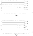
- FIG. 3 illustrates a partial structural schematic diagram of a display panel according to another embodiment of the disclosure.
- FIG. 4 illustrates a partial cross-sectional structural schematic diagram, in the direction B 1 -B 2 in FIG. 3 , of a display panel according to an embodiment of the disclosure.
- FIG. 5 illustrates a partial cross-sectional structural schematic diagram, in the direction B 1 -B 2 in FIG. 3 , of a display panel according to another embodiment of the disclosure.
- FIG. 6 illustrates a partial cross-sectional structural schematic diagram, in the direction B 1 -B 2 in FIG. 3 , of a display panel according to another embodiment of the disclosure.
- an embodiment of the disclosure provides a display panel, including:
- a driving backplane 1 wherein the driving backplane 1 includes a display area, the display area is provided with a heterotypic edge 100 , and the display area includes a plurality of first pixel opening areas 11 and a plurality of second pixel opening areas 12 ; wherein the plurality of first pixel opening areas 11 are close to the heterotypic edge 100 , and the plurality of second pixel opening areas 12 are away from the heterotypic edge 100 ; and
- a light emitting structure 2 wherein the light emitting structure 2 is arranged on the driving backplane 1 and includes a plurality of functional layers, wherein the plurality of functional layers include a first functional layer 20 , each second pixel opening area 12 is completely covered by the first functional layer 20 , and each first pixel opening area 11 is only partially covered by the first functional layer 20 ;
- an edge part 200 , covering the first pixel opening areas 11 , of the first functional layer 20 is a smooth edge
- an area, where the first functional layer 20 covers, of the first pixel opening areas 11 and the second pixel opening areas 12 is an effective display area.
- the ‘pixel opening areas’ correspond to sub-pixel openings, and each ‘pixel opening area’ corresponds to a projection of a sub-pixel opening.
- the ‘display area’ refers to a sub-pixel arrangement area of the driving backplane, and the edge of the display area surrounds all sub-pixels and extends along the edge sub-pixels; and the ‘heterotypic edge’ refers to a section, in a jagged form due to the arrangement of the edge sub-pixels, of the edge of the display area.
- the above-mentioned heterotypic edge 100 may be only part of the edge of the display area, of course, it may also be the entire edge of the display area.
- the ‘smooth edge’ means that the edge boundary is a smooth line.
- the ‘smooth edge’ can change with the bending of the edge contour of the driving backplane and is roughly similar to the edge contour of the driving backplane in shape.
- the ‘smooth edge’ may be a smooth arc; at a wavy border area of the driving backplane, the ‘smooth edge’ may be a smooth wavy line; and when the edge of the driving backplane is a circular contour, the ‘smooth edge’ may be a circular arc.
- the display panel provided by the embodiment of the disclosure includes the driving backplane 1 and the light emitting structure 2 ; wherein the display area of the driving backplane 1 is provided with the heterotypic edge 100 , that is, the display panel is a heterotypic panel; and the light emitting structure 2 is provided with a plurality of functional layers covering the display area for realizing light emission.
- a conventional heterotypic panel the edges of all functional layers of a light emitting structure go beyond the edge of a display area, and pixel opening areas in the display area are effective display areas, as a result, after the panel is turned on, all the pixel opening areas emit light, and a jagged form formed by the arrangement of edge sub-pixels of the display area is presented at the edges of the effective display areas, that is, a heterotypic edge is presented.
- the first functional layer 20 in the light emitting structure 2 does not cover the whole display area, specifically, each of the first pixel opening areas 11 near the heterotypic edge 100 is only partially covered by the first functional layer 20 , in other words, the edge part 200 , near the heterotypic edge 100 , of the first functional layer 20 is within the first pixel opening areas 11 (in the display area).
- the area, where the first functional layer 20 covers, of the first pixel opening areas 11 and the second pixel opening areas 12 defines the effective display area, after the panel is turned on, all the second pixel opening areas 12 emit light, and only partial first pixel opening areas 11 emit light, so the edge part 200 (smooth edge) of the first functional layer 20 on the first pixel opening areas 11 is presented, instead of the heterotypic edge 100 of the display area. Therefore, in the heterotypic display panel according to the embodiment of the disclosure, jagged edges will not appear, so that the visual experience of products can be improved.
- edges 201 of the functional layers other than the first functional layer 20 all go beyond the edge of the display area, that is, the functional layers other than the first functional layer 20 cover all the pixel opening areas in the display area.
- the display area of the driving backplane 1 further includes third pixel opening areas 13 , and the third pixel opening areas 13 are located between the first pixel opening areas 11 and the heterotypic edge 100 of the display area.
- the third pixel opening areas 13 are adjacent to the heterotypic edge 100 and are not covered by the first functional layer 20 , thus belonging to an ineffective display area. That is, when the display panel is turned on, the third pixel opening areas 13 do not emit light, so they can also be called dummy pixel opening areas.
- the third pixel opening areas 13 can separate the heterotypic edge 100 from the effective display areas by a set distance to better avoid the display of jagged edges.
- the spacing between the heterotypic edge 100 and the smooth edge of the first functional layer 20 may be set to a spacing of one to three third pixel opening areas 13 .
- one to three circles of third pixel opening areas 13 may be arranged along the contour of the heterotypic edge or the smooth edge.
- the sizes of the first pixel opening areas 11 , the sizes of the second pixel opening areas 12 and the sizes of the third pixel opening areas 13 are the same.
- the driving backplane includes a pixel defining structure (PDL) 4 , and the PDL 4 is configured to form the pixel opening areas defining the display area.
- the edge shape of the display area is determined by the arrangement form of edge sub-pixels defined by the PDL 4 .
- the dashed line boundary shown in FIG. 1 is the edge shape of the display area.
- the display panel provided by the embodiment of the disclosure further includes a first electrode layer 5 located on the side, facing away from the driving backplane 1 , of the light emitting structure 2 , and the first electrode layer 5 completely covering the display area.
- a first electrode layer 5 located on the side, facing away from the driving backplane 1 , of the light emitting structure 2 , and the first electrode layer 5 completely covering the display area.
- an edge 300 of the first electrode layer may go beyond the edge of the display area, and the first electrode layer completely covers the display area.
- the first electrode layer is a cathode layer.
- a peripheral cathode trace (VSS) 400 electrically connected to the cathode layer is located between the edges 201 of the functional layers and the edge 300 of the cathode layer, and is disposed around the display area.
- the cathode layer may not completely cover the peripheral cathode trace (VSS) 400 , or the edge 300 of the cathode layer is located on the side, close to the inside of the display area, of the cathode trace (VSS) 400 , for example, partially overlapping, or being connected through other conductive layers.
- the driving backplane 1 further includes second electrodes 10 in one-to-one correspondence to the pixel opening areas, and the orthographic projection of each pixel opening area is within the orthographic projection of the corresponding second electrode 10 , that is, the projections of the second electrodes 10 completely cover the projections of the pixel opening areas in the display area.
- the second electrodes 10 are anodes.
- the size of the second electrode 10 corresponding to the first pixel opening area 11 , the size of the second pixel opening area 12 , and the size of the third pixel opening area 13 are the same; and the shape of the second electrode 10 corresponding to the first pixel opening area 11 , the shape of the second pixel opening area 12 , and the shape of the third pixel opening area 13 are the same.
- the second electrodes 10 corresponding to the second pixel opening areas 12 inside the display area include light emitting structures emitting different colors of light
- the second electrodes 10 corresponding to the second pixel opening areas 12 may have different shapes and sizes; for example, the shape of the second electrode corresponding to the light emitting structure emitting red light, the shape of the second electrode corresponding to the light emitting structure emitting green light and the shape of the second electrode corresponding to the light emitting structure emitting blue light are different; and the size of the second electrode corresponding to the light emitting structure emitting red light, the size of the second electrode corresponding to the light emitting structure emitting green light and the size of the second electrode corresponding to the light emitting structure emitting blue light are different; or the shapes and sizes of the second electrodes corresponding to the light emitting structures in two colors are different, then the second electrode corresponding to a first pixel opening area 11 may correspondingly have the same shape and size as the second electrode 10 corresponding to the light emitting structure in one color in the display area, and the second electrode 10 corresponding to
- the shapes and sizes of the second electrodes 10 corresponding to the first pixel opening areas 11 are partially the same. In some embodiments, the shapes and sizes of the second electrodes 10 corresponding to the third pixel opening areas 13 are partially the same and partially different. In some embodiments, second electrodes 10 may not be arranged for the third pixel opening areas 13 . In some embodiments, according to the pixel arrangement structure, the luminescent material layer in the third pixel opening areas 13 corresponding to the position of the subpixel of the same color may be the same as the luminescent material layer in the second pixel opening areas 12 , i.e.
- the luminescent material layer in the first pixel opening areas 11 corresponding to the position of the subpixel of the same color may be the same as the luminescent material layer in the second pixel opening areas 12 , i.e. completely covering pixel openings.
- the luminescent material layer in the first pixel opening area 11 and the luminescent material layer in the third pixel opening area 13 are manufactured with the same process as the luminescent material layer in the second pixel opening area 12 , for example, the luminescent material of the same color is evaporated by an evaporation process, so that the quality of film layers in the luminescent material layer in the second pixel opening areas 12 inside the display area is more reliable and uniform, thus ensuring the display quality of an actual luminescent area.
- each edge sub-pixel opening is heterotypic, thus making the edge of the display area regular.
- This solution can also avoid the display of jagged edges.
- due to the heavy workload of heterotypic drawing of each sub-pixel and the difficulty in controlling the heterotypic angle in the drawing process this solution is difficult to design and realize.
- the size of an opening of an open mask used in evaporation of an organic functional layer can be appropriately reduced, so that the heterotypic edge of the display area does not emit light by reducing the evaporation area, thus avoiding the display of jagged edges.
- the solution of the embodiment of the disclosure is simpler and easier to implement.
- a plurality of functional layers of the light emitting structure 2 include at least one of a hole injection layer 21 , a hole transport layer 22 , a luminescent material layer 23 , an electron transport layer 24 or an electron injection layer 25 ; and the first functional layer 20 includes at least one of the plurality of functional layers.
- edges of the portions, located in the first pixel opening areas, of the film layers in the first functional layer 20 are aligned.
- the first functional layer 20 includes a luminescent material layer and at least one of the hole injection layer 21 , the hole transport layer 22 , the electron transport layer 24 or the electron injection layer 25 .
- the luminescent material layer is patterned and covers at least the second pixel opening areas and part of the first pixel opening areas.
- At least one of the hole injection layer 21 , the hole transport layer 22 , the electron transport layer 24 or the electron injection layer 25 is a whole film layer. Edges of the portions, located in the first pixel opening areas, of at least one of the luminescent layer, the hole injection layer 21 , the hole transport layer 22 , the electron transport layer 24 or the electron injection layer 25 are aligned.
- Edges of the portions, located in the first pixel opening areas, of the functional layers in the first functional layer 20 are aligned, so that the functional layers in the first functional layer 20 can share one mask or one kind of masks, thereby simplifying the evaporation process and reducing cost.
- ‘one kind of masks’ refers to masks with the same opening pattern.
- each film layer in the first functional layer 20 is a continuous whole film layer. That is, each functional layer in the first functional layer 20 is a whole film layer covering the effective display areas instead of patterns distributed in an array corresponding to sub-pixel openings.
- each functional layer can adopt an open mask, and an evaporation opening of the open mask is a large opening covering sub-pixel openings instead of an opening array in one-to-one correspondence to sub-pixel openings. In this way, by reducing the area of the large opening, an evaporation edge of the first functional layer 20 is within the heterotypic edge 100 of the display area, so that the heterotypic edge 100 of the display area does not emit light, thereby preventing the appearance of jagged edges.
- the embodiment of the disclosure has very simple requirements on an opening pattern of the mask and is very easy to realize.
- the ‘continuous whole film layer’ refers to a film layer evaporated as a whole.
- the surface of the substrate will have relatively large segment differences, which may lead to film layer breakage, but the projection of the film layer on the substrate is continuous. Therefore, in the embodiment of the disclosure, the ‘continuous whole film layer’ refers to the continuous projection of the film layer, including the case of film layer breakage.
- the light emitting structure 2 includes OLED devices in one color, and each film layer in the plurality of functional layers of the light emitting structure 2 is a continuous whole film layer. In this way, the mask requirement on each film layer is very simple, and each film layer may be configured as the first functional layer 20 .
- the luminescent material layer 23 may be configured as the first functional layer 20 , or, as shown in FIG. 5 , the hole transport layer 22 may be configured as the first functional layer 20 , or, as shown in FIG. 6 , the luminescent material layer 23 and the hole transport layer 22 may be jointly configured as the first functional layer 20 .
- the light emitting structure 2 includes OLED devices in different colors, a plurality of functional layers include at least two functional layers, and one or two of the hole injection layer 21 , the hole transport layer 22 , the luminescent material layer 23 , the electron transport layer 24 and the electron injection layer 25 are provided with patterns.
- the light emitting structure 2 may include OLED devices in three colors, i.e., red, green and blue colors.
- each film layer is a continuous whole film layer, and the luminescent material layer 23 is provided with patterns distributed in an array, and includes luminescent materials for light emitting devices in different colors, which need to be evaporated separately.
- the mask requirement on each film layer is very simple, and each film layer may be configured as the first functional layer 20 .
- the hole transport layer 22 may also be provided with patterns distributed in an array. In order to adjust the light emitting colors of sub-pixels in various colors, the thickness of the hole transport layer 22 may vary for sub-pixels in various colors.
- the first functional layer 20 may include the hole transport layer 22 .
- the film layers in the first functional layer may not be whole film layers but be provided with patterns distributed in an array.
- evaporation may be conducted by overlaying an open mask with a fine metal mask (FMM).
- the patterns can be obtained through the FMM, and the edge of the functional layer can be defined by the open mask.
- the luminescent material layer is provided with patterns distributed in an array, and the luminescent material layer may be configured as the first functional layer.
- evaporation may be conducted by overlaying the open mask with the FMM, and the evaporation edge of the luminescent material layer can be adjusted by changing the opening of the open mask.
- the hole transport layer may also be configured as the first functional layer.
- the embodiments of the disclosure also provide a display device, including any one of the display panels described above.
- the display device may be a heterotypic product, specifically may be a lighting device, such as a lamp piece of a car lamp, or a display, a tablet personal computer, a smart phone, etc.
- a lighting device such as a lamp piece of a car lamp, or a display, a tablet personal computer, a smart phone, etc.
- the embodiments of the disclosure further provide a method for preparing a display panel, including:
- FIGS. 1 to 6 forming a light emitting structure 2 on a driving backplane 1 ;
- each second pixel opening area 12 is completely covered by the first functional layer 20 , and each first pixel opening area 11 is only partially covered by the first functional layer 20 ; an edge part 200 , covering the first pixel opening areas 11 , of the first functional layer 20 is a smooth edge;
- an area, where the first functional layer 20 covers, of the first pixel opening areas 11 and the second pixel opening areas 12 is an effective display area.
- the operation of forming the first functional layer in the light emitting structure includes:
- the first functional layer includes at least one of a hole injection layer, a hole transport layer, a luminescent material layer, an electron transport layer or an electron injection layer.
- the operation of evaporating the film layers of the first functional layer sequentially by the evaporation process includes:
- each functional layer in the first functional layer may be a whole film layer covering the effective display area
- each film layer in the first functional layer may adopt an open mask
- an evaporation opening of the open mask is a large opening covering sub-pixel openings instead of an array of openings in one-to-one correspondence to sub-pixel openings.
- an evaporation edge of the first functional layer is within the heterotypic edge of the display area, so that the heterotypic edge of the display area does not emit light, thereby preventing the appearance of jagged edges.
- the first functional layer may also include a film layer with patterns.
- evaporation may be conducted by overlaying an open mask with a fine metal mask (FMM).
- the patterns can be obtained through the FMM, and the edge of the functional layer can be defined by the open mask.
- the luminescent material layer is provided with patterns distributed in an array, and the luminescent material layer may be configured as the first functional layer.
- evaporation may be conducted by overlaying the open mask with the FMM, and the evaporation edge of the luminescent material layer can be adjusted by changing the opening of the open mask.
- the hole transport layer may also be configured as the first functional layer.
- the functional layers, except the first functional layer completely cover the pixel opening areas in the display area, and the functional layers, except the first functional layer, may also share one mask or one kind of masks.
- the method before preparing the light emitting structure on the driving backplane 1 , the method further includes the step of preparing a pixel defining structure 4 on the driving backplane 1 . Further, after the light emitting structure is prepared on the driving backplane 1 , the method also includes the step of preparing second electrodes 6 and an encapsulation layer (not shown in the figure) on the driving backplane 1 sequentially.
- the preparation process of the display panel generally includes: (1) preparing the second electrodes 10 on the driving backplane 1 , (2) preparing the pixel defining structure 4 , (3) evaporating the light emitting structure (including the first functional layer 20 ), (4) preparing a first electrode layer 5 , (5) preparing the encapsulation layer.
Landscapes
- Engineering & Computer Science (AREA)
- Physics & Mathematics (AREA)
- Chemical & Material Sciences (AREA)
- Optics & Photonics (AREA)
- Microelectronics & Electronic Packaging (AREA)
- Manufacturing & Machinery (AREA)
- Materials Engineering (AREA)
- Organic Chemistry (AREA)
- Metallurgy (AREA)
- Mechanical Engineering (AREA)
- Chemical Kinetics & Catalysis (AREA)
- Electroluminescent Light Sources (AREA)
- Devices For Indicating Variable Information By Combining Individual Elements (AREA)
Abstract
Description
Claims (14)
Applications Claiming Priority (2)
| Application Number | Priority Date | Filing Date | Title |
|---|---|---|---|
| CN201911327955.7 | 2019-12-20 | ||
| CN201911327955.7A CN111063716A (en) | 2019-12-20 | 2019-12-20 | Display panel, preparation method thereof and display device |
Publications (2)
| Publication Number | Publication Date |
|---|---|
| US20210193750A1 US20210193750A1 (en) | 2021-06-24 |
| US11489017B2 true US11489017B2 (en) | 2022-11-01 |
Family
ID=70302517
Family Applications (1)
| Application Number | Title | Priority Date | Filing Date |
|---|---|---|---|
| US16/928,121 Active US11489017B2 (en) | 2019-12-20 | 2020-07-14 | Display panel, method for preparing display panel, and display device |
Country Status (2)
| Country | Link |
|---|---|
| US (1) | US11489017B2 (en) |
| CN (1) | CN111063716A (en) |
Families Citing this family (2)
| Publication number | Priority date | Publication date | Assignee | Title |
|---|---|---|---|---|
| CN112234089B (en) * | 2020-10-16 | 2022-07-29 | 青岛三顺智能电器有限公司 | OLED display panel and display screen |
| CN113074351B (en) * | 2021-04-07 | 2023-05-16 | 固安翌光科技有限公司 | OLED lamp sheet and OLED car lamp |
Citations (23)
| Publication number | Priority date | Publication date | Assignee | Title |
|---|---|---|---|---|
| US20130002127A1 (en) * | 2011-06-29 | 2013-01-03 | Hee-Seong Jeong | Organic light-emitting display device |
| US20160218124A1 (en) * | 2013-09-27 | 2016-07-28 | Boe Technology Group Co., Ltd. | Thin film transistor driving backplane and manufacturing method thereof, and display panel |
| US20160343944A1 (en) * | 2015-05-19 | 2016-11-24 | Samsung Display Co., Ltd. | Masks, method to inspect and adjust mask position, and method to pattern pixels of organic light-emitting display device utilizing the masks |
| US20180026080A1 (en) * | 2016-07-25 | 2018-01-25 | Samsung Display Co., Ltd. | Display device |
| US20180144675A1 (en) * | 2016-11-22 | 2018-05-24 | Samsung Display Co., Ltd. | Flat panel display device having display areas with the appearance of rounded corners |
| CN108470753A (en) | 2018-03-28 | 2018-08-31 | 京东方科技集团股份有限公司 | A kind of electroluminescence display panel, its production method and display device |
| US20180269397A1 (en) * | 2017-11-07 | 2018-09-20 | Shanghai Tianma AM-OLED Co., Ltd. | Organic electroluminescent display panel, method for manufacturing the same, and display device |
| US20180337217A1 (en) * | 2016-02-02 | 2018-11-22 | Boe Technology Group Co., Ltd. | Display substrate, display panel, and display apparatus |
| US20190088709A1 (en) * | 2017-09-19 | 2019-03-21 | Xiamen Tianma Micro-Electronics Co., Ltd. | Display panel and display apparatus |
| US20190140026A1 (en) * | 2016-07-08 | 2019-05-09 | Sharp Kabushiki Kaisha | Display panel |
| US20190173011A1 (en) * | 2017-12-05 | 2019-06-06 | Lg Display Co., Ltd. | Electroluminescent display device |
| US20190181201A1 (en) * | 2017-12-11 | 2019-06-13 | Lg Display Co., Ltd. | Electroluminescent Display Device |
| US20190206973A1 (en) * | 2017-12-28 | 2019-07-04 | Lg Display Co., Ltd. | Electroluminescence display apparatus |
| US10379397B1 (en) * | 2018-05-31 | 2019-08-13 | Wuhan China Star Optoelectronics Technology Co., Ltd. | Method and structure for improving display quality of irregular shaped panel |
| CN110323346A (en) * | 2019-03-29 | 2019-10-11 | 昆山国显光电有限公司 | Display panel and display device |
| US20200202817A1 (en) * | 2018-07-23 | 2020-06-25 | Ordos Yuansheng Optoelectronics Co., Ltd. | Display optimization method and apparatus, display driving method and apparatus, display apparatus, and storage medium |
| US20200219944A1 (en) * | 2018-11-15 | 2020-07-09 | Wuhan China Star Optoelectronics Semiconductor Display Technology Co., Ltd. | Active-matrix organic light emitting diode display panel structure |
| US20210066428A1 (en) * | 2019-08-28 | 2021-03-04 | Shanghai Tianma AM-OLED Co., Ltd. | Display Panel with Irregular Shape and Display Device |
| US20210202615A1 (en) * | 2019-12-31 | 2021-07-01 | Lg Display Co., Ltd. | Display device |
| US20210202611A1 (en) * | 2019-12-31 | 2021-07-01 | Lg Display Co., Ltd. | Display panel |
| US20210233967A1 (en) * | 2017-12-07 | 2021-07-29 | Boe Technology Group Co., Ltd. | Display panel, display apparatus, and method of fabricating display panel |
| US11256127B2 (en) * | 2017-05-10 | 2022-02-22 | Boe Technology Group Co., Ltd. | Display substrate, display panel and display device |
| US11282898B2 (en) * | 2018-06-12 | 2022-03-22 | Ordos Yuansheng Optoelectronics Co., Ltd. | Display substrate, method for manufacturing same, and display device |
-
2019
- 2019-12-20 CN CN201911327955.7A patent/CN111063716A/en active Pending
-
2020
- 2020-07-14 US US16/928,121 patent/US11489017B2/en active Active
Patent Citations (27)
| Publication number | Priority date | Publication date | Assignee | Title |
|---|---|---|---|---|
| US20130002127A1 (en) * | 2011-06-29 | 2013-01-03 | Hee-Seong Jeong | Organic light-emitting display device |
| US20160218124A1 (en) * | 2013-09-27 | 2016-07-28 | Boe Technology Group Co., Ltd. | Thin film transistor driving backplane and manufacturing method thereof, and display panel |
| US20160343944A1 (en) * | 2015-05-19 | 2016-11-24 | Samsung Display Co., Ltd. | Masks, method to inspect and adjust mask position, and method to pattern pixels of organic light-emitting display device utilizing the masks |
| US20180337217A1 (en) * | 2016-02-02 | 2018-11-22 | Boe Technology Group Co., Ltd. | Display substrate, display panel, and display apparatus |
| US20190140026A1 (en) * | 2016-07-08 | 2019-05-09 | Sharp Kabushiki Kaisha | Display panel |
| US20180026080A1 (en) * | 2016-07-25 | 2018-01-25 | Samsung Display Co., Ltd. | Display device |
| US11233097B2 (en) * | 2016-07-25 | 2022-01-25 | Samsung Display Co., Ltd. | Display device including dummy pixels with transmissive areas |
| US20180144675A1 (en) * | 2016-11-22 | 2018-05-24 | Samsung Display Co., Ltd. | Flat panel display device having display areas with the appearance of rounded corners |
| US11256127B2 (en) * | 2017-05-10 | 2022-02-22 | Boe Technology Group Co., Ltd. | Display substrate, display panel and display device |
| US20190088709A1 (en) * | 2017-09-19 | 2019-03-21 | Xiamen Tianma Micro-Electronics Co., Ltd. | Display panel and display apparatus |
| US20180269397A1 (en) * | 2017-11-07 | 2018-09-20 | Shanghai Tianma AM-OLED Co., Ltd. | Organic electroluminescent display panel, method for manufacturing the same, and display device |
| US20190173011A1 (en) * | 2017-12-05 | 2019-06-06 | Lg Display Co., Ltd. | Electroluminescent display device |
| US20210233967A1 (en) * | 2017-12-07 | 2021-07-29 | Boe Technology Group Co., Ltd. | Display panel, display apparatus, and method of fabricating display panel |
| US11139345B2 (en) * | 2017-12-07 | 2021-10-05 | Boe Technology Group Co., Ltd. | Display panel, display apparatus, and method of fabricating display panel |
| US20190181201A1 (en) * | 2017-12-11 | 2019-06-13 | Lg Display Co., Ltd. | Electroluminescent Display Device |
| US20190206973A1 (en) * | 2017-12-28 | 2019-07-04 | Lg Display Co., Ltd. | Electroluminescence display apparatus |
| US10872938B2 (en) * | 2018-03-28 | 2020-12-22 | Boe Technology Group Co., Ltd. | Electroluminescent display panel, method for fabricating the same and display device |
| US20190305057A1 (en) * | 2018-03-28 | 2019-10-03 | Boe Technology Group Co., Ltd. | Electroluminescent display panel, method for fabricating the same and display device |
| CN108470753A (en) | 2018-03-28 | 2018-08-31 | 京东方科技集团股份有限公司 | A kind of electroluminescence display panel, its production method and display device |
| US10379397B1 (en) * | 2018-05-31 | 2019-08-13 | Wuhan China Star Optoelectronics Technology Co., Ltd. | Method and structure for improving display quality of irregular shaped panel |
| US11282898B2 (en) * | 2018-06-12 | 2022-03-22 | Ordos Yuansheng Optoelectronics Co., Ltd. | Display substrate, method for manufacturing same, and display device |
| US20200202817A1 (en) * | 2018-07-23 | 2020-06-25 | Ordos Yuansheng Optoelectronics Co., Ltd. | Display optimization method and apparatus, display driving method and apparatus, display apparatus, and storage medium |
| US20200219944A1 (en) * | 2018-11-15 | 2020-07-09 | Wuhan China Star Optoelectronics Semiconductor Display Technology Co., Ltd. | Active-matrix organic light emitting diode display panel structure |
| CN110323346A (en) * | 2019-03-29 | 2019-10-11 | 昆山国显光电有限公司 | Display panel and display device |
| US20210066428A1 (en) * | 2019-08-28 | 2021-03-04 | Shanghai Tianma AM-OLED Co., Ltd. | Display Panel with Irregular Shape and Display Device |
| US20210202615A1 (en) * | 2019-12-31 | 2021-07-01 | Lg Display Co., Ltd. | Display device |
| US20210202611A1 (en) * | 2019-12-31 | 2021-07-01 | Lg Display Co., Ltd. | Display panel |
Non-Patent Citations (2)
| Title |
|---|
| Machine translation, Li, Chinese Pat. Pub. No. CN 110323346A, translation date: Jan. 7, 2022, Espacenet, all pages. (Year: 2022). * |
| Office Action from corresponding Chinese application 201911327955.7 dated Nov. 29, 2021. |
Also Published As
| Publication number | Publication date |
|---|---|
| US20210193750A1 (en) | 2021-06-24 |
| CN111063716A (en) | 2020-04-24 |
Similar Documents
| Publication | Publication Date | Title |
|---|---|---|
| US10790339B2 (en) | OLED array substrate and manufacturing method thereof, and display device | |
| CN109192076B (en) | Display panel and display device | |
| US9859352B2 (en) | Transparent organic light emitting display device and method of manufacturing the same | |
| WO2018014562A1 (en) | Pixel arrangement structure, display substrate, display apparatus and method of fabrication thereof | |
| CN109585490B (en) | Pixel defining layer, ink-jet printing method, display substrate, manufacturing method of display substrate and display device | |
| KR20220162837A (en) | Display panel, manufacturing method of display panel, and display device | |
| US20070046195A1 (en) | Organic light-emitting display and fabricating method thereof | |
| EP4036979A1 (en) | Transparent display substrate, transparent display panel, and display device | |
| EP3187937B1 (en) | Mask plate, mask plate assembly and use of mask plate assembly for pixel manufacturing | |
| US9660000B2 (en) | Organic light emitting diode (OLED) array substrate and fabricating method thereof, display device | |
| CN111584605B (en) | Array substrate, preparation method, display panel and display device | |
| US11489017B2 (en) | Display panel, method for preparing display panel, and display device | |
| US10096774B2 (en) | Evaporation method and evaporation device | |
| US11024676B2 (en) | Organic light-emitting diode display panel and manufacturing method thereof, and display device | |
| CN107680990B (en) | Pixel arrangement structure, pixel structure, manufacturing method and display method | |
| US20170040388A1 (en) | Electroluminescent display and display device | |
| WO2022205931A1 (en) | Oled display substrate, and display apparatus | |
| EP3203522A1 (en) | Oled display substrate, oled display device and mask plate | |
| JP2016018782A (en) | Organic light-emitting element and element arrangement | |
| CN109962096A (en) | Show backboard and preparation method thereof, display device | |
| CN105006479A (en) | Display substrate and display device applying same | |
| US10522775B2 (en) | El display device including island shaped hole injection layer and island shaped electron injection layer and method of manufacturing the same | |
| CN108364991A (en) | Organic light-emitting diode display substrate and preparation method thereof, display device | |
| CN104637972A (en) | High-resolution organic light emitting display and manufacturing method thereof | |
| CN110085624B (en) | Pixel arrangement structure, display panel and mask plate assembly |
Legal Events
| Date | Code | Title | Description |
|---|---|---|---|
| AS | Assignment |
Owner name: BOE TECHNOLOGY GROUP CO., LTD., CHINA Free format text: ASSIGNMENT OF ASSIGNORS INTEREST;ASSIGNORS:SHI, KUNYAN;WU, POHSIEN;REEL/FRAME:053199/0457 Effective date: 20200525 Owner name: CHENGDU BOE OPTOELECTRONICS TECHNOLOGY CO., LTD., CHINA Free format text: ASSIGNMENT OF ASSIGNORS INTEREST;ASSIGNORS:SHI, KUNYAN;WU, POHSIEN;REEL/FRAME:053199/0457 Effective date: 20200525 |
|
| FEPP | Fee payment procedure |
Free format text: ENTITY STATUS SET TO UNDISCOUNTED (ORIGINAL EVENT CODE: BIG.); ENTITY STATUS OF PATENT OWNER: LARGE ENTITY |
|
| STPP | Information on status: patent application and granting procedure in general |
Free format text: DOCKETED NEW CASE - READY FOR EXAMINATION |
|
| STPP | Information on status: patent application and granting procedure in general |
Free format text: NON FINAL ACTION MAILED |
|
| STPP | Information on status: patent application and granting procedure in general |
Free format text: RESPONSE TO NON-FINAL OFFICE ACTION ENTERED AND FORWARDED TO EXAMINER |
|
| STPP | Information on status: patent application and granting procedure in general |
Free format text: FINAL REJECTION MAILED |
|
| STPP | Information on status: patent application and granting procedure in general |
Free format text: NOTICE OF ALLOWANCE MAILED -- APPLICATION RECEIVED IN OFFICE OF PUBLICATIONS |
|
| AS | Assignment |
Owner name: BEIJING BOE TECHNOLOGY DEVELOPMENT CO., LTD., CHINA Free format text: ASSIGNMENT OF ASSIGNORS INTEREST;ASSIGNOR:BOE TECHNOLOGY GROUP CO., LTD.;REEL/FRAME:060650/0805 Effective date: 20220726 |
|
| STPP | Information on status: patent application and granting procedure in general |
Free format text: PUBLICATIONS -- ISSUE FEE PAYMENT RECEIVED |
|
| STPP | Information on status: patent application and granting procedure in general |
Free format text: PUBLICATIONS -- ISSUE FEE PAYMENT VERIFIED |
|
| STCF | Information on status: patent grant |
Free format text: PATENTED CASE |