EP3187923A1 - Camera module integrated liquid display device and manufacturing method thereof - Google Patents
Camera module integrated liquid display device and manufacturing method thereof Download PDFInfo
- Publication number
- EP3187923A1 EP3187923A1 EP16197689.9A EP16197689A EP3187923A1 EP 3187923 A1 EP3187923 A1 EP 3187923A1 EP 16197689 A EP16197689 A EP 16197689A EP 3187923 A1 EP3187923 A1 EP 3187923A1
- Authority
- EP
- European Patent Office
- Prior art keywords
- lens hole
- array substrate
- liquid
- display device
- crystal display
- Prior art date
- Legal status (The legal status is an assumption and is not a legal conclusion. Google has not performed a legal analysis and makes no representation as to the accuracy of the status listed.)
- Granted
Links
Images




Classifications
-
- G—PHYSICS
- G02—OPTICS
- G02F—OPTICAL DEVICES OR ARRANGEMENTS FOR THE CONTROL OF LIGHT BY MODIFICATION OF THE OPTICAL PROPERTIES OF THE MEDIA OF THE ELEMENTS INVOLVED THEREIN; NON-LINEAR OPTICS; FREQUENCY-CHANGING OF LIGHT; OPTICAL LOGIC ELEMENTS; OPTICAL ANALOGUE/DIGITAL CONVERTERS
- G02F1/00—Devices or arrangements for the control of the intensity, colour, phase, polarisation or direction of light arriving from an independent light source, e.g. switching, gating or modulating; Non-linear optics
- G02F1/01—Devices or arrangements for the control of the intensity, colour, phase, polarisation or direction of light arriving from an independent light source, e.g. switching, gating or modulating; Non-linear optics for the control of the intensity, phase, polarisation or colour
- G02F1/13—Devices or arrangements for the control of the intensity, colour, phase, polarisation or direction of light arriving from an independent light source, e.g. switching, gating or modulating; Non-linear optics for the control of the intensity, phase, polarisation or colour based on liquid crystals, e.g. single liquid crystal display cells
- G02F1/133—Constructional arrangements; Operation of liquid crystal cells; Circuit arrangements
- G02F1/1333—Constructional arrangements; Manufacturing methods
-
- G—PHYSICS
- G06—COMPUTING OR CALCULATING; COUNTING
- G06F—ELECTRIC DIGITAL DATA PROCESSING
- G06F1/00—Details not covered by groups G06F3/00 - G06F13/00 and G06F21/00
- G06F1/16—Constructional details or arrangements
- G06F1/1601—Constructional details related to the housing of computer displays, e.g. of CRT monitors, of flat displays
- G06F1/1605—Multimedia displays, e.g. with integrated or attached speakers, cameras, microphones
-
- G—PHYSICS
- G02—OPTICS
- G02F—OPTICAL DEVICES OR ARRANGEMENTS FOR THE CONTROL OF LIGHT BY MODIFICATION OF THE OPTICAL PROPERTIES OF THE MEDIA OF THE ELEMENTS INVOLVED THEREIN; NON-LINEAR OPTICS; FREQUENCY-CHANGING OF LIGHT; OPTICAL LOGIC ELEMENTS; OPTICAL ANALOGUE/DIGITAL CONVERTERS
- G02F1/00—Devices or arrangements for the control of the intensity, colour, phase, polarisation or direction of light arriving from an independent light source, e.g. switching, gating or modulating; Non-linear optics
- G02F1/01—Devices or arrangements for the control of the intensity, colour, phase, polarisation or direction of light arriving from an independent light source, e.g. switching, gating or modulating; Non-linear optics for the control of the intensity, phase, polarisation or colour
- G02F1/13—Devices or arrangements for the control of the intensity, colour, phase, polarisation or direction of light arriving from an independent light source, e.g. switching, gating or modulating; Non-linear optics for the control of the intensity, phase, polarisation or colour based on liquid crystals, e.g. single liquid crystal display cells
- G02F1/133—Constructional arrangements; Operation of liquid crystal cells; Circuit arrangements
- G02F1/136—Liquid crystal cells structurally associated with a semi-conducting layer or substrate, e.g. cells forming part of an integrated circuit
-
- G—PHYSICS
- G02—OPTICS
- G02F—OPTICAL DEVICES OR ARRANGEMENTS FOR THE CONTROL OF LIGHT BY MODIFICATION OF THE OPTICAL PROPERTIES OF THE MEDIA OF THE ELEMENTS INVOLVED THEREIN; NON-LINEAR OPTICS; FREQUENCY-CHANGING OF LIGHT; OPTICAL LOGIC ELEMENTS; OPTICAL ANALOGUE/DIGITAL CONVERTERS
- G02F1/00—Devices or arrangements for the control of the intensity, colour, phase, polarisation or direction of light arriving from an independent light source, e.g. switching, gating or modulating; Non-linear optics
- G02F1/01—Devices or arrangements for the control of the intensity, colour, phase, polarisation or direction of light arriving from an independent light source, e.g. switching, gating or modulating; Non-linear optics for the control of the intensity, phase, polarisation or colour
- G02F1/13—Devices or arrangements for the control of the intensity, colour, phase, polarisation or direction of light arriving from an independent light source, e.g. switching, gating or modulating; Non-linear optics for the control of the intensity, phase, polarisation or colour based on liquid crystals, e.g. single liquid crystal display cells
- G02F1/133—Constructional arrangements; Operation of liquid crystal cells; Circuit arrangements
- G02F1/1333—Constructional arrangements; Manufacturing methods
- G02F1/1335—Structural association of cells with optical devices, e.g. polarisers or reflectors
- G02F1/133509—Filters, e.g. light shielding masks
- G02F1/133512—Light shielding layers, e.g. black matrix
-
- G—PHYSICS
- G02—OPTICS
- G02F—OPTICAL DEVICES OR ARRANGEMENTS FOR THE CONTROL OF LIGHT BY MODIFICATION OF THE OPTICAL PROPERTIES OF THE MEDIA OF THE ELEMENTS INVOLVED THEREIN; NON-LINEAR OPTICS; FREQUENCY-CHANGING OF LIGHT; OPTICAL LOGIC ELEMENTS; OPTICAL ANALOGUE/DIGITAL CONVERTERS
- G02F1/00—Devices or arrangements for the control of the intensity, colour, phase, polarisation or direction of light arriving from an independent light source, e.g. switching, gating or modulating; Non-linear optics
- G02F1/01—Devices or arrangements for the control of the intensity, colour, phase, polarisation or direction of light arriving from an independent light source, e.g. switching, gating or modulating; Non-linear optics for the control of the intensity, phase, polarisation or colour
- G02F1/13—Devices or arrangements for the control of the intensity, colour, phase, polarisation or direction of light arriving from an independent light source, e.g. switching, gating or modulating; Non-linear optics for the control of the intensity, phase, polarisation or colour based on liquid crystals, e.g. single liquid crystal display cells
- G02F1/133—Constructional arrangements; Operation of liquid crystal cells; Circuit arrangements
- G02F1/1333—Constructional arrangements; Manufacturing methods
- G02F1/1335—Structural association of cells with optical devices, e.g. polarisers or reflectors
- G02F1/133528—Polarisers
-
- G—PHYSICS
- G02—OPTICS
- G02F—OPTICAL DEVICES OR ARRANGEMENTS FOR THE CONTROL OF LIGHT BY MODIFICATION OF THE OPTICAL PROPERTIES OF THE MEDIA OF THE ELEMENTS INVOLVED THEREIN; NON-LINEAR OPTICS; FREQUENCY-CHANGING OF LIGHT; OPTICAL LOGIC ELEMENTS; OPTICAL ANALOGUE/DIGITAL CONVERTERS
- G02F1/00—Devices or arrangements for the control of the intensity, colour, phase, polarisation or direction of light arriving from an independent light source, e.g. switching, gating or modulating; Non-linear optics
- G02F1/01—Devices or arrangements for the control of the intensity, colour, phase, polarisation or direction of light arriving from an independent light source, e.g. switching, gating or modulating; Non-linear optics for the control of the intensity, phase, polarisation or colour
- G02F1/13—Devices or arrangements for the control of the intensity, colour, phase, polarisation or direction of light arriving from an independent light source, e.g. switching, gating or modulating; Non-linear optics for the control of the intensity, phase, polarisation or colour based on liquid crystals, e.g. single liquid crystal display cells
- G02F1/133—Constructional arrangements; Operation of liquid crystal cells; Circuit arrangements
- G02F1/136—Liquid crystal cells structurally associated with a semi-conducting layer or substrate, e.g. cells forming part of an integrated circuit
- G02F1/1362—Active matrix addressed cells
- G02F1/136286—Wiring, e.g. gate line, drain line
-
- G—PHYSICS
- G03—PHOTOGRAPHY; CINEMATOGRAPHY; ANALOGOUS TECHNIQUES USING WAVES OTHER THAN OPTICAL WAVES; ELECTROGRAPHY; HOLOGRAPHY
- G03B—APPARATUS OR ARRANGEMENTS FOR TAKING PHOTOGRAPHS OR FOR PROJECTING OR VIEWING THEM; APPARATUS OR ARRANGEMENTS EMPLOYING ANALOGOUS TECHNIQUES USING WAVES OTHER THAN OPTICAL WAVES; ACCESSORIES THEREFOR
- G03B29/00—Combinations of cameras, projectors or photographic printing apparatus with non-photographic non-optical apparatus, e.g. clocks or weapons; Cameras having the shape of other objects
-
- G—PHYSICS
- G06—COMPUTING OR CALCULATING; COUNTING
- G06F—ELECTRIC DIGITAL DATA PROCESSING
- G06F1/00—Details not covered by groups G06F3/00 - G06F13/00 and G06F21/00
- G06F1/16—Constructional details or arrangements
- G06F1/1613—Constructional details or arrangements for portable computers
- G06F1/1633—Constructional details or arrangements of portable computers not specific to the type of enclosures covered by groups G06F1/1615 - G06F1/1626
- G06F1/1637—Details related to the display arrangement, including those related to the mounting of the display in the housing
-
- G—PHYSICS
- G06—COMPUTING OR CALCULATING; COUNTING
- G06F—ELECTRIC DIGITAL DATA PROCESSING
- G06F1/00—Details not covered by groups G06F3/00 - G06F13/00 and G06F21/00
- G06F1/16—Constructional details or arrangements
- G06F1/1613—Constructional details or arrangements for portable computers
- G06F1/1633—Constructional details or arrangements of portable computers not specific to the type of enclosures covered by groups G06F1/1615 - G06F1/1626
- G06F1/1684—Constructional details or arrangements related to integrated I/O peripherals not covered by groups G06F1/1635 - G06F1/1675
- G06F1/1686—Constructional details or arrangements related to integrated I/O peripherals not covered by groups G06F1/1635 - G06F1/1675 the I/O peripheral being an integrated camera
-
- H—ELECTRICITY
- H04—ELECTRIC COMMUNICATION TECHNIQUE
- H04N—PICTORIAL COMMUNICATION, e.g. TELEVISION
- H04N23/00—Cameras or camera modules comprising electronic image sensors; Control thereof
- H04N23/50—Constructional details
- H04N23/51—Housings
-
- H—ELECTRICITY
- H04—ELECTRIC COMMUNICATION TECHNIQUE
- H04N—PICTORIAL COMMUNICATION, e.g. TELEVISION
- H04N23/00—Cameras or camera modules comprising electronic image sensors; Control thereof
- H04N23/57—Mechanical or electrical details of cameras or camera modules specially adapted for being embedded in other devices
-
- G—PHYSICS
- G02—OPTICS
- G02F—OPTICAL DEVICES OR ARRANGEMENTS FOR THE CONTROL OF LIGHT BY MODIFICATION OF THE OPTICAL PROPERTIES OF THE MEDIA OF THE ELEMENTS INVOLVED THEREIN; NON-LINEAR OPTICS; FREQUENCY-CHANGING OF LIGHT; OPTICAL LOGIC ELEMENTS; OPTICAL ANALOGUE/DIGITAL CONVERTERS
- G02F1/00—Devices or arrangements for the control of the intensity, colour, phase, polarisation or direction of light arriving from an independent light source, e.g. switching, gating or modulating; Non-linear optics
- G02F1/01—Devices or arrangements for the control of the intensity, colour, phase, polarisation or direction of light arriving from an independent light source, e.g. switching, gating or modulating; Non-linear optics for the control of the intensity, phase, polarisation or colour
- G02F1/13—Devices or arrangements for the control of the intensity, colour, phase, polarisation or direction of light arriving from an independent light source, e.g. switching, gating or modulating; Non-linear optics for the control of the intensity, phase, polarisation or colour based on liquid crystals, e.g. single liquid crystal display cells
- G02F1/133—Constructional arrangements; Operation of liquid crystal cells; Circuit arrangements
- G02F1/13306—Circuit arrangements or driving methods for the control of single liquid crystal cells
- G02F1/13312—Circuits comprising photodetectors for purposes other than feedback
-
- G—PHYSICS
- G02—OPTICS
- G02F—OPTICAL DEVICES OR ARRANGEMENTS FOR THE CONTROL OF LIGHT BY MODIFICATION OF THE OPTICAL PROPERTIES OF THE MEDIA OF THE ELEMENTS INVOLVED THEREIN; NON-LINEAR OPTICS; FREQUENCY-CHANGING OF LIGHT; OPTICAL LOGIC ELEMENTS; OPTICAL ANALOGUE/DIGITAL CONVERTERS
- G02F1/00—Devices or arrangements for the control of the intensity, colour, phase, polarisation or direction of light arriving from an independent light source, e.g. switching, gating or modulating; Non-linear optics
- G02F1/01—Devices or arrangements for the control of the intensity, colour, phase, polarisation or direction of light arriving from an independent light source, e.g. switching, gating or modulating; Non-linear optics for the control of the intensity, phase, polarisation or colour
- G02F1/13—Devices or arrangements for the control of the intensity, colour, phase, polarisation or direction of light arriving from an independent light source, e.g. switching, gating or modulating; Non-linear optics for the control of the intensity, phase, polarisation or colour based on liquid crystals, e.g. single liquid crystal display cells
- G02F1/133—Constructional arrangements; Operation of liquid crystal cells; Circuit arrangements
- G02F1/1333—Constructional arrangements; Manufacturing methods
- G02F1/133388—Constructional arrangements; Manufacturing methods with constructional differences between the display region and the peripheral region
-
- G—PHYSICS
- G02—OPTICS
- G02F—OPTICAL DEVICES OR ARRANGEMENTS FOR THE CONTROL OF LIGHT BY MODIFICATION OF THE OPTICAL PROPERTIES OF THE MEDIA OF THE ELEMENTS INVOLVED THEREIN; NON-LINEAR OPTICS; FREQUENCY-CHANGING OF LIGHT; OPTICAL LOGIC ELEMENTS; OPTICAL ANALOGUE/DIGITAL CONVERTERS
- G02F1/00—Devices or arrangements for the control of the intensity, colour, phase, polarisation or direction of light arriving from an independent light source, e.g. switching, gating or modulating; Non-linear optics
- G02F1/01—Devices or arrangements for the control of the intensity, colour, phase, polarisation or direction of light arriving from an independent light source, e.g. switching, gating or modulating; Non-linear optics for the control of the intensity, phase, polarisation or colour
- G02F1/13—Devices or arrangements for the control of the intensity, colour, phase, polarisation or direction of light arriving from an independent light source, e.g. switching, gating or modulating; Non-linear optics for the control of the intensity, phase, polarisation or colour based on liquid crystals, e.g. single liquid crystal display cells
- G02F1/133—Constructional arrangements; Operation of liquid crystal cells; Circuit arrangements
- G02F1/1333—Constructional arrangements; Manufacturing methods
- G02F1/1335—Structural association of cells with optical devices, e.g. polarisers or reflectors
- G02F1/133509—Filters, e.g. light shielding masks
- G02F1/133514—Colour filters
-
- G—PHYSICS
- G02—OPTICS
- G02F—OPTICAL DEVICES OR ARRANGEMENTS FOR THE CONTROL OF LIGHT BY MODIFICATION OF THE OPTICAL PROPERTIES OF THE MEDIA OF THE ELEMENTS INVOLVED THEREIN; NON-LINEAR OPTICS; FREQUENCY-CHANGING OF LIGHT; OPTICAL LOGIC ELEMENTS; OPTICAL ANALOGUE/DIGITAL CONVERTERS
- G02F1/00—Devices or arrangements for the control of the intensity, colour, phase, polarisation or direction of light arriving from an independent light source, e.g. switching, gating or modulating; Non-linear optics
- G02F1/01—Devices or arrangements for the control of the intensity, colour, phase, polarisation or direction of light arriving from an independent light source, e.g. switching, gating or modulating; Non-linear optics for the control of the intensity, phase, polarisation or colour
- G02F1/13—Devices or arrangements for the control of the intensity, colour, phase, polarisation or direction of light arriving from an independent light source, e.g. switching, gating or modulating; Non-linear optics for the control of the intensity, phase, polarisation or colour based on liquid crystals, e.g. single liquid crystal display cells
- G02F1/133—Constructional arrangements; Operation of liquid crystal cells; Circuit arrangements
- G02F1/1333—Constructional arrangements; Manufacturing methods
- G02F1/1339—Gaskets; Spacers; Sealing of cells
-
- H—ELECTRICITY
- H04—ELECTRIC COMMUNICATION TECHNIQUE
- H04N—PICTORIAL COMMUNICATION, e.g. TELEVISION
- H04N23/00—Cameras or camera modules comprising electronic image sensors; Control thereof
- H04N23/50—Constructional details
Definitions
- the inventors of the application have devised an LCD device with minimal thickness and having a lens hole in an array substrate of the LCD device, into which a lens unit of a camera module or some other functional element can be inserted.
- the lens hole is formed in the array substrate with a drill or similar equipment.
- an element A on an element B refers to that the element A may be disposed directly on the element B and/or the element A may be disposed indirectly on the element B via another element C.
- first, second and the like in the descriptions and in the claims are used for distinguishing between similar elements and not necessarily for describing a sequential or chronological order. Theses terms are used to merely distinguish one element from another. Accordingly, as used herein, a first element may be a second element within the technical idea of the present disclosure.
- the second polarization plate 125 may be disposed on the top surface of the color filter substrate 120 and may absorb polarized light depending on a tilt angle of the polarization axis of the light polarized by the liquid-crystal layer 115.
- a variety of drivers may be disposed on the array substrate 1110 in the peripheral area PA.
- the drives may include a gate driver configured to apply signals to the gate lines, and a data driver configured to apply signals to the data lines.
- the drivers may be attached to the pad unit PAD formed in the periphery area PA by a conductive adhesive or may be formed together with switching elements on the array substrate during the process of forming the same. It is to be noted that the LCD device 100 according to the exemplary embodiment of the present disclosure is not limited by the drivers and the pad unit.
- the measurement pattern 175 is made of a metal material and thus is opaque. Accordingly, measurement error of the confocal sensor can be reduced by use of the measurement pattern 175.
- the shape of the measurement pattern 175 is not limited to those described above but may have a variety of shapes as long as measurements with the confocal sensor can be more accurately performed.
- the aperture 160 may be formed by patterning the black matrix 130.
- the diameter L5 of the aperture 160 may be determined based on the view angle ⁇ of the camera module 140. For example, there may be a particular distance between the lens part 140a and the aperture 160. The distance is also associated with the thickness of the overcoat layer 135. That is, the aperture 160 may be configured so that it does not hide or obstruct the viewing angle ⁇ of the camera module 140. If the aperture 160 hides or obstructs the viewing angle ⁇ of the camera module 140, the camera module 140 cannot properly perform image capturing due to the covered part. However, it is to be noted that the aperture 160 may also be configured so that it hides a part of the viewing angle ⁇ of the camera module 140.
- the overcoat layer 135 on the color filter substrate 120 in the peripheral area PA covers the black matrix 130 and the aperture 160.
- the overcoat layer 135 may reduce the step difference (or layer unevenness) between the black matrix 130 and the aperture 160 or may provide a flat surface. Further, the overcoat layer 135 may transmit light of the visible wavelength band.
- the camera module 140 can effectively capture images through the transparent portion 165 of the second polarization plate 125.
- the center of the lens hole and a center of the lens hole guide may be configured to be adjacent to each other.
- An inner edge of the lens hole guide may be spaced apart from an edge of the lens hole.
- the LCD device may further include: a first polarization plate disposed under the array substrate; and a second polarization plate disposed on the color filter substrate.
- the second polarization plate may cover the aperture and comprises a transparent portion in line with the aperture.
- the measurement pattern may have a circular ring shape or a donut shape.
Landscapes
- Physics & Mathematics (AREA)
- Engineering & Computer Science (AREA)
- Nonlinear Science (AREA)
- General Physics & Mathematics (AREA)
- Theoretical Computer Science (AREA)
- Computer Hardware Design (AREA)
- Optics & Photonics (AREA)
- Mathematical Physics (AREA)
- Chemical & Material Sciences (AREA)
- Crystallography & Structural Chemistry (AREA)
- General Engineering & Computer Science (AREA)
- Human Computer Interaction (AREA)
- Multimedia (AREA)
- Signal Processing (AREA)
- Microelectronics & Electronic Packaging (AREA)
- Liquid Crystal (AREA)
- Devices For Indicating Variable Information By Combining Individual Elements (AREA)
- Geometry (AREA)
Abstract
an array substrate (110) on which a sub-pixel is disposed; a color filter substrate (120) on which a color filter corresponding to the sub-pixel is disposed; and a liquid-crystal layer (115) between the array substrate (110) and the color filter substrate (120). The array substrate (110) comprises a lens hole (150), the color filter substrate (120) comprises a lens hole guide (155), and a diameter of the lens hole (150) is smaller than an inner diameter of the lens hole guide (155).
Description
- This application claims the priority of
Korean Patent Application No. 10-2015-0187173 filed on December 28, 2015 - The present disclosure relates to a liquid-crystal display (LCD), and more particularly, to a liquid-crystal display device including a lens hole for a camera module and a method of fabricating the same.
- An LCD device is a transmissive display device and includes a liquid-crystal panel and a backlight unit. The liquid-crystal panel includes an array substrate for controlling a liquid-crystal layer, a polarization plate disposed on a surface of the array substrate, a color filter substrate facing the array substrate, a polarization plate disposed on a surface of the color filter substrate, and the liquid-crystal layer disposed between the array substrate and the color filter substrate. The liquid-crystal panel controls the liquid-crystal layer to thereby adjust transmittance of each of sub-pixels of the liquid-crystal panel.
- The backlight unit includes optical sheets, a light guide plate, a light source unit, a reflective plate, and a guide panel. The optical sheets are disposed between the liquid-crystal panel and the light guide plate. For example, the optical sheets may include a prism film and/or a diffusion film. The light source is disposed on the side surface of the light guide plate, such that light is diffused through the light guide plate. The reflective plate is disposed on the bottom surface of the light guide plate to reflect light leaking toward the reflective plate. The guide panel supports the optical sheets, the light guide plate, the light source and the reflective plate, etc., to allow the liquid-crystal panel to be stably mounted thereon.
- The inventors of the application have studied and developed an LCD device into which a camera module (or portion thereof), a user-pressable button, etc. can be inserted.
- The inventors of the application have devised an LCD device with minimal thickness and having a lens hole in an array substrate of the LCD device, into which a lens unit of a camera module or some other functional element can be inserted. Specifically, the lens hole is formed in the array substrate with a drill or similar equipment.
- However, the present inventors recognized many problems caused during the process of forming such hole. For example, the hole itself or portions of the substrate may be damaged during the drilling process.
- Further, after certain elements on a surface of the array substrate are formed, the desired hole may need to be formed at a location having several transparent material layers respectively having different refractive indexes. Accordingly, there may be an error in measuring the precise depth or thickness at the location where the hole is to be formed, such that the substrate may be damaged when the lens hole is formed with the drill or similar equipment based on inaccurate thickness measurements. The thinness of the substrate, which may or may not have certain layers thereon, requires very precise hole drilling. Doing so needs to be based upon accurate substrate thickness measurements, in order to prevent inaccurate drilling (i.e. over-drilling or under-drilling) and to minimize roughness or burrs at the inner surface of the hole.
- Accordingly, the present invention is directed to a camera module integrated liquid crystal display device and manufacturing method thereof that substantially obviate one or more of the problems due to limitations and disadvantages as described above.
- An object of the present disclosure is to provide an LCD device with minimal thickness to receive a camera module inserted thereinto while suppressing damages to the substrate that may occur during the fabricating process, and a method of fabricating the same.
- Additional features and advantages of the invention will be set forth in the description that follows, and in part will be apparent from the description, or may be learned by practice of the invention. The objectives and other advantages will be realized and attained by the exemplary structures and methods particularly pointed out in the written description, and claims hereof as well as the appended drawings.
- To achieve these and other advantages and in accordance with the inventive concepts as embodied and broadly described, a liquid-crystal display (LCD) device comprises an array substrate on which a sub-pixel is disposed; a color filter substrate on which a color filter corresponding to the sub-pixel is disposed; and a liquid-crystal layer between the array substrate and the color filter substrate. The array substrate comprises a lens hole, the color filter substrate comprises a lens hole guide, and a diameter of the lens hole is smaller than an inner diameter of the lens hole guide.
- In another aspect, a method of fabricating a liquid-crystal display (LCD) device comprises measuring a thickness of an array substrate with a confocal sensor by using a measurement pattern on the array substrate; forming a groove in a position where a lens hole is to be formed to a depth determined based on the thickness of the array substrate measured with the confocal sensor; attaching a glass core to a region where the groove is formed by applying adhesion with a taping equipment, and then separating the glass core from the array substrate with the taping equipment to thereby form the lens hole; and inserting a camera module into the array substrate through the lens hole.
- Particulars in the exemplary embodiments of the present disclosure will be described in the detail description with reference to the accompanying drawings.
- According to an exemplary embodiment of the present disclosure, the thickness of an LCD device can be reduced even if a camera module is inserted thereinto by way of forming a lens hole in the array substrate to insert the camera module into the lens hole.
- In addition, according to an exemplary embodiment of the present disclosure, a lens part is inserted into the lens hole and the lens hole guide, such that the camera module can capture images through a color filter substrate.
- Further, according to an exemplary embodiment of the present disclosure, a lens hole guide is formed around the lens hole, such that damage to the array substrate can be suppressed by the lens hole guide during the process of forming the lens hole in the array substrate.
- Moreover, according to an exemplary embodiment of the present disclosure, defects during the process of forming the lens hole can be reduced by a measurement pattern.
- It is to be understood that both the foregoing general description and the following detailed description are exemplary and explanatory and are intended to provide further explanation of the invention as claimed.
- The accompanying drawings, which are included to provide a further understanding of the invention and are incorporated in and constitute a part of this specification, illustrate embodiments of the invention and together with the description serve to explain the principles of the invention. In the drawings:
-
FIG. 1 is a schematic plan view of an LCD device according to an exemplary embodiment of the present disclosure; -
FIG. 2 is a schematic perspective view of an LCD device and a camera module according to an exemplary embodiment of the present disclosure; -
FIG. 3 is a cross-sectional view taken along line A - A and a camer -
FIG. 4 is an enlarged cross-sectional view ofFIG. 3 ; and -
FIGs. 5A to 5C are cross-sectional views for illustrating a method for forming a lens hole of an LCD device according to another exemplary embodiment of the present disclosure. - Reference will now be made in detail to some embodiments of the present invention, examples of which are illustrated in the accompanying drawings.
- The figures, dimensions, ratios, angles, the numbers of elements given in the drawings are merely illustrative and are not limiting. Like reference numerals denote like elements throughout the descriptions. Further, in describing the present disclosure, descriptions on well-known technologies may be omitted in order not to unnecessarily obscure the gist of the present disclosure. It is to be noticed that the terms "comprising," "having," "including" and so on, used in the description and claims, should not be interpreted as being restricted to the means listed thereafter unless specifically stated otherwise. Where an indefinite or definite article is used when referring to a singular noun, e.g. "a," "an," "the," this includes a plural of that noun unless specifically stated otherwise.
- In describing elements, they are interpreted as including error margins even without explicit statements.
- In describing positional relationship, such as "an element A on an element B," "an element A above an element B," "an element A below an element B," and "an element A next to an element B," another element C may be disposed between the elements A and B unless the term "directly" or "immediately" is explicitly used.
- As used herein, a phrase "an element A on an element B" refers to that the element A may be disposed directly on the element B and/or the element A may be disposed indirectly on the element B via another element C.
- The terms first, second and the like in the descriptions and in the claims are used for distinguishing between similar elements and not necessarily for describing a sequential or chronological order. Theses terms are used to merely distinguish one element from another. Accordingly, as used herein, a first element may be a second element within the technical idea of the present disclosure.
- Like reference numerals denote like elements throughout the descriptions. The drawings are not to scale and the relative dimensions of various elements in the drawings are depicted schematically and not necessarily to scale.
- Features of various exemplary embodiments of the present disclosure may be combined partially or totally. As will be clearly appreciated by those skilled in the art, technically various interactions and operations are possible. Various exemplary embodiments can be practiced individually or in combination.
-
FIG. 1 is a schematic plan view of an LCD device according to an exemplary embodiment of the present disclosure. - With reference to
FIG. 1 , anLCD device 100 according to an exemplary embodiment of the present disclosure may include a pixel area AA in which a plurality of pixels is disposed, and a peripheral area PA surrounding the pixel area AA. In the peripheral area PA, a pad unit PAD is disposed such that a variety of driver units are attached thereon. For example, a gate driver or a data driver may be attached thereto. In addition, acamera module 140 is inserted in the periphery area PA. -
FIG. 2 is a schematic perspective view of an LCD device and a camera module according to an exemplary embodiment of the present disclosure. - With reference to
FIG. 2 , theLCD device 100 according to the exemplary embodiment of the present disclosure includes anarray substrate 110, alens hole 150 formed in thearray substrate 110, ameasurement pattern 175 disposed around thelens hole 150, alens hole guide 155 in line with thelens hole 150, anovercoat layer 135 disposed above thelens hole guide 155, ablack matrix 130 disposed on theovercoat layer 135 and including anaperture 160 in line with thelens hole 150, acolor filter substrate 120 disposed on theblack matrix 130, and asecond polarization plate 125 disposed on thecolor filter substrate 120 and having atransparent portion 165. - The
camera module 140 can include alens part 140a and asensor part 140b. Thelens 140a (or a portion thereof) is inserted into thelens hole 150. - The
lens part 140a can include a lens and a guide for supporting the lens. Thelens part 140a may have a cylindrical shape. However, this is merely illustrative. - The
sensor part 140a can include an image sensor for converting an image having passed thelens part 140a into an electric signal, and a circuit board on which the image sensor is disposed. However, this is merely illustrative. - The camera module 140 (or a portion thereof) is inserted into the
lens hole 150 on thearray substrate 110. TheLCD device 100 has an advantage in that the overall thickness or space occupied by thecamera module 140 can be reduced by inserting thecamera module 140 into thelens hole 150. - The
lens part 140a is inserted into thelens hole 150 and thelens hole guide 155. Accordingly, there is an advantage in that thecamera module 140 can capture images via theaperture 160. -
FIG. 3 is a cross-sectional view taken along line A - A' ofFIG. 1 . -
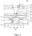
FIG. 4 is an enlarged, cross-sectional view ofFIG. 3 . - With reference to
FIGs. 3 to 4 , theLCD device 100 according to the exemplary embodiment of the present disclosure includes thearray substrate 110 including thelens hole 150 and thecolor filter substrate 120 including theaperture 160. Thecamera module 140 is inserted into thelens hole 150 of theLCD device 100. Afirst polarization plate 105 may be disposed on the bottom surface of thearray substrate 110 and may polarize light supplied from the light source unit. - A liquid-
crystal layer 115 is disposed between thearray substrate 110 and thecolor filter substrate 120. Liquid-crystal molecules in the liquid-crystal layer 115 are tilted by signals applied from pixel electrodes and common electrodes of a sub-pixel. As the liquid-crystal molecules are tilted, transmittance of each of the sub-pixels of theLCD device 100 is adjusted. - A
sealant 117 surrounds the outer periphery of the liquid-crystal layer 115 disposed between thearray substrate 110. and thecolor filter substrate 120. Accordingly, the liquid-crystal layer 115 is sealed by thesealent 117. - The
second polarization plate 125 may be disposed on the top surface of thecolor filter substrate 120 and may absorb polarized light depending on a tilt angle of the polarization axis of the light polarized by the liquid-crystal layer 115. - The
LCD device 100 may include a pixel area AA and a peripheral area PA. - A sub-pixel for driving the liquid-
crystal layer 115 is disposed on thearray substrate 110 in the pixel area AA. The sub-pixel may include: a pixel electrode; a common electrode corresponding to the pixel electrode; a data line configured to apply image signals to the pixel electrode; a gate line configured to apply a turn-on signal to the pixel electrode; a switching element configured to apply image signals to the pixel electrode by receiving the signal applied from the gate line and the data line; insulation films for insulating elements from one another; and an alignment layer disposed on the liquid-crystal layer 115 to align liquid-crystal molecules in the liquid-crystal layer 115. It is to be noted that theLCD device 100 according to the exemplary embodiment of the present disclosure are not limited by the elements of the pixel area AA. Acolor filter 122 and theblack matrix 130 are disposed on thecolor filter substrate 120 in the pixel area AA. Thecolor filter 122 may include red, green and blue color filters. The black matrix separates thecolor filters 122 from one another. Theovercoat layer 135 covers thecolor filter 122 and theblack matrix 130 to reduce or planarize the step difference created by thecolor filter 122 and theblack matrix 130. An alignment layer may be disposed between theovercoat layer 135 and the liquid-crystal layer 115 to align the liquid-crystal molecules. It is to be noted that theLCD device 100 according to the exemplary embodiment of the present disclosure are not limited by the elements of the pixel area AA. - In some embodiments of the present disclosure, the common electrode may be formed on the color filter substrate. For example, for a vertical alignment (VA) or twisted nematic (TN) LCD device, the common electrode may be formed on the color filter substrate.
- In some embodiments of the present disclosure, the color filter may be included in a sub-pixel. For example, for a color-filter on thin-film-transistor (COT) LCD device, the color filter may be formed on the array substrate.
- A variety of drivers may be disposed on the array substrate 1110 in the peripheral area PA. The drives may include a gate driver configured to apply signals to the gate lines, and a data driver configured to apply signals to the data lines. The drivers may be attached to the pad unit PAD formed in the periphery area PA by a conductive adhesive or may be formed together with switching elements on the array substrate during the process of forming the same. It is to be noted that the
LCD device 100 according to the exemplary embodiment of the present disclosure is not limited by the drivers and the pad unit. - The lens hole 150 (or similar aperture or opening for accommodating some element) may be formed in the
array substrate 110 in the peripheral area PA. More than onelens hole 150 may be formed. Thecamera module 140 may be inserted into thelens hole 150. - The
lens hole 150 may be formed by penetrating thearray substrate 110 with a drill or similar equipment. The drill may have a tip made of diamond. The tip of the drill may have a ring shape and may form a ring or hole in thearray substrate 110 as it rotates at high speed. The diameter L1 of thelens hole 150 may be determined depending on the diameter of the drill. For example, the diameter L1 of thelens hole 150 may range from 4 mm to 6 mm. However, this is merely exemplary. - The
camera module 140 may be inserted into thelens hole 150. Thecamera module 140 includes thelens part 140a and thesensor part 140b. - The
lens part 140a may include a lens and a mold for supporting the lens. Thelens part 140a has a viewing angle. Thelens part 140a may have a cylindrical shape. It is to be noted that the shape of thelens part 140a is not limited to the cylindrical shape but may have different shapes depending on the shape of the mold. - The
lens hole 150 may have a shape corresponding to thelens part 140a. That is, thelens hole 150 conforms to thelens part 140a so that thelens part 140a or a portion thereof can be inserted into thelens hole 150. For example, if thelens part 140a has a circular shape, thelens hole 150 may also have the circular shape. The diameter L1 of thelens hole 150 may be equal to or larger than the diameter L2 of the outer side surface of thelens part 140a of thecamera module 140. With the above-described configuration, thelens part 140a may be inserted into thelens hole 150. Accordingly, the thickness of theLCD device 100 including thecamera module 140 can be reduced. - The
sensor part 140b may include a circuit board and an image sensor. Thesensor part 140b converts images captured by thelens part 140a into electric signals. The image signals output from thesensor part 140b may be transmitted to another system via lines. - The measurement pattern 175 (or similar element configured to improve measurements) is disposed at, near, or around the
lens hole 150 in thearray substrate 110. Themeasurement pattern 175 may have a shape corresponding to thelens hole 150. In order to form thelens hole 150 in thearray substrate 110, it is necessary to measure the thickness of thearray substrate 110 at a location where the hole is to be formed. Specifically, since there may be minute deviations in the overall thickness of thearray substrate 110, it may be necessary to measure the precise thickness where the hole is to be formed. - The thickness of the
array substrate 110 may be measured with a confocal sensor or some other measuring equipment. In addition, it is also necessary to reduce measurement errors in measuring the thickness of thearray substrate 110 with a confocal sensor. - The
measurement pattern 175 may be made of at least one of metal materials of the gate line or the data line on thearray substrate 110. For example, themeasurement pattern 175 may be made of at least one of copper, aluminum, molybdenum and titanium. With the above-described configuration, no additional process is required for forming themeasurement pattern 175, and thus themeasurement pattern 175 can be formed by modifying a shape of a mask. Accordingly, an additional mask may not be required to form themeasurement pattern 175. - The
measurement pattern 175 is disposed on the top surface of thearray substrate 110. Accordingly, by measuring the distance from the bottom surface of thearray substrate 110 to themeasurement pattern 175, the thickness of thearray substrate 110 and how deep thearray substrate 110 has to be drilled for forming thelens hole 150 can be measured. - The
measurement pattern 175 may have a shape corresponding to thelens hole 150. For example, themeasurement pattern 175 may have a circular shape, such as a ring or a donut shape if thelens hole 150 has a circular shape. Themeasurement pattern 175 has a particular width and/or diameter. For example, the width of the ring-like measurement pattern 175 may range from 200 µm to 700 µm. It is to be noted that theLCD device 100 according to the exemplary embodiment of the present disclosure is not limited by the width and/or diameter of themeasurement pattern 175. - With the above-described configuration, the thickness of the
array substrate 110 can be measured more accurately using a confocal sensor by measuring the thickness of thearray substrate 100 having themeasurement pattern 175 at the hole formation location. - For example, the thickness of the
array substrate 110 may range from 150 µm to 400 µm. More specifically, if the thickness of thearray substrate 110 is 250 µm, for example, the confocal sensor measures the distance from the bottom surface of thearray substrate 110 to themeasurement pattern 175 disposed on the top surface of thearray substrate 110. Accordingly, the thickness of thearray substrate 110 can be measured more accurately when compared to the thickness measurement performed without themeasurement pattern 175. - The
measurement pattern 175 is made of a metal material and thus is opaque. Accordingly, measurement error of the confocal sensor can be reduced by use of themeasurement pattern 175. The shape of themeasurement pattern 175 is not limited to those described above but may have a variety of shapes as long as measurements with the confocal sensor can be more accurately performed. - Without the
measurement pattern 175, there are only transparent materials at and around the lens hole location of the LCD device. Accordingly, it is difficult to accurately measure the thickness of the array substrate with just the confocal sensor. Due to such inaccurate measurements, the hole formed in thearray substrate 110 with the drill may be too shallow. As a result, the lens hole may not be formed as desired. - On the other hand, the hole formed in the
array substrate 110 with the drill may be too deep. Specifically, the hole may reach theblack matrix 130 formed on thecolor filter substrate 120. As a result, glass pieces or debris may be generated when thelens hole 150 is formed, and defects due to such foreign matter may occur. In addition, theblack matrix 130 may be damaged. As a result, light may leak from the damagedblack matrix 130. - The inner diameter L3 of the
measurement pattern 175 may be larger than the diameter L1 of thelens hole 150. With the above-described configuration, themeasurement pattern 175 does not come in contact with the drill even if thelens hole 150 is formed by the drill because the inner diameter L3 of themeasurement pattern 175 is larger than the diameter of the drill. Accordingly, themeasurement pattern 175 is not damaged by the drill. - In some embodiments of the present disclosure, the outer diameter of the
measurement pattern 175 may be equal to or smaller than the diameter L1 of thelens hole 150. With the above-described configuration, themeasurement pattern 175 can be effectively removed during the process of forming thelens hole 150 with the drill because the outer diameter of themeasurement pattern 175 is smaller than the diameter of the drill. Specifically, the thickness of thearray substrate 110 is more accurately measured with the confocal sensor with respect to themeasurement pattern 175, and then thelens hole 150 is formed in thearray substrate 100 with the drill based on the accurately measured thickness. That is, the measurement pattern may be removed once the thickness of thearray substrate 110 has been measured. Accordingly, the measurement pattern may be removed during the process of forming thelens hole 150. Alternatively, only a part of the measurement pattern may be removed while the rest may remain around thelens hole 150. - The
lens hole guide 155 in line with thelens hole 150 is formed in thecolor filter substrate 120 in the peripheral area PA. Thelens hole guide 155 is in line with thelens hole 150. Thelens hole guide 155 may support thearray substrate 110 around thelens hole 150. For example, if thelens part 140a of thecamera module 140 is a cylindrical shape, thelens hole 150 may be a circular shape, and the inner side of thelens hole guide 155 may also be the circular shape. The center of thelens hole 150 may be adjacent to or in line (i.e. aligned) with the center of thelens hole guide 155. Thelens hole guide 155 is made of an organic material or an inorganic material. - Specifically, the
array substrate 110 is ground by a drill during the process of forming thelens hole 150 with the drill. Thearray substrate 110 may be made of glass. There may be space between thearray substrate 110 and thecolor filter substrate 120. As thearray substrate 120 receives pressure from the drill process, undesired physical impact may be exerted onto thearray substrate 120. As a result, thearray substrate 120 may be undesirably bent and cracks or other deformities may occur. In addition, while thearray substrate 110 is ground by the drill, small glass pieces or debris may scatter around thelens hole 150. - The
lens hole guide 155 surrounds thelens hole 150 to minimize or suppress thearray substrate 120 from being bent when physical impact is exerted on thearray substrate 120, thereby reducing cracks in thearray substrate 120. That is, thelens hole guide 155 can effectively absorb at least some of the impact, pressure or force exerted on thearray substrate 110 during the process of forming thelens hole 150. - In addition, as the
lens hole guide 155 surrounds thelens hole 150, it can block the glass pieces from scattering. Accordingly, the glass pieces or debris are restricted within thelens hole 150, such that it is more convenient to remove such debris or pieces in thelens hole 150 by using a tool, such as a suction means, for removing them. - With reference to
FIG. 4 , the inner diameter L4 of thelens hole guide 155 may be larger than the diameter L1 of thelens hole 150. With the above-described configuration, thelens hole guide 155 may be effectively prevented from coming into contact with the drill during the process of forming thelens hole 150 with the drill. Accordingly, damage to thelens hole guide 155 may be minimized. - Although the inner side of the
lens hole guide 155 conforms to thelens hole 150, the outer side of thelens hole guide 155 may or may not conform to it and thus can have different shapes. For example, the periphery of thelens hole guide 155 may be a circular shape, a rectangular shape, a polygonal shape, a streamlined shape, etc. - The
lens hole guide 155 and themeasurement pattern 175 may overlap one another. With the above-described configuration, themeasurement pattern 175 may cover thelens hole guide 155. Accordingly, it is possible to reduce the measurement error by thelens hole guide 155 during the process measuring the thickness of the array substrate 110 (having the measurement pattern 175) with the confocal sensor. - Specifically, the
lens hole guide 155 may have a refractive index different from that of thearray substrate 110 and may be optically transparent. This may result in measurement errors. It is to be noted that in theLCD device 100 according to the exemplary embodiment of the present disclosure, thelens hole guide 155 and themeasurement pattern 175 may not overlap but may be spaced apart from each other. - The
black matrix 130 covers at least a part of thecolor filter substrate 120 in the peripheral area PA. Theblack matrix 130 is disposed between thecolor filter substrate 120 and thelens hole guide 155. For example, theblack matrix 130 may cover at least some portion of themeasurement pattern 175. With the above-described configuration, themeasurement pattern 175 may be covered by theblack matrix 130. In addition, theblack matrix 130 may cover the peripheral area PA. With the above-described configuration, light from the light source via the peripheral area PA can be effectively shielded, and that themeasurement pattern 175 disposed around thelens hole 150 is hidden by theblack matrix 130 such that external light is not undesirably reflected off themeasurement pattern 175. - In the
black matrix 130 on thecolor filter substrate 120 in the periphery area PA, theaperture 160 in line or aligned with thecamera module 140 is formed. - The
aperture 160 may be formed by patterning theblack matrix 130. The diameter L5 of theaperture 160 may be determined based on the view angle θ of thecamera module 140. For example, there may be a particular distance between thelens part 140a and theaperture 160. The distance is also associated with the thickness of theovercoat layer 135. That is, theaperture 160 may be configured so that it does not hide or obstruct the viewing angle θ of thecamera module 140. If theaperture 160 hides or obstructs the viewing angle θ of thecamera module 140, thecamera module 140 cannot properly perform image capturing due to the covered part. However, it is to be noted that theaperture 160 may also be configured so that it hides a part of the viewing angle θ of thecamera module 140. - The diameter L5 of the
aperture 160 may be smaller than the diameter L1 of thelens hole 150. The center of theaperture 160 may be adjacent to or aligned with the center of thelens hole 150. With the above-described configuration, theaperture 160 may hide the rest of thecamera module 140 without hiding the viewing angle θ. Accordingly, the unnecessary part of thecamera module 140 is hidden by theaperture 160, such that the aesthetic design can be improved. It is to be noted that theLCD device 100 according to the exemplary embodiment of the present disclosure is not limited by that. - The
overcoat layer 135 on thecolor filter substrate 120 in the peripheral area PA covers theblack matrix 130 and theaperture 160. Theovercoat layer 135 may reduce the step difference (or layer unevenness) between theblack matrix 130 and theaperture 160 or may provide a flat surface. Further, theovercoat layer 135 may transmit light of the visible wavelength band. - The
overcoat layer 135 may reduce the step difference between theblack matrix 130 and theaperture 160 to have a gentle (or gradual) slope. However, light may be refracted by the gentle slope, and thus the viewing angle θ of thecamera module 140 may not overlap the sloped surface. - Alternatively, the viewing angle θ of the
camera module 140 may overlap the sloped surface, and a compensation value for compensating such distortion may be stored in a memory. It is to be noted that theLCD device 100 according to the exemplary embodiment of the present disclosure is not limited by the sloped surface of theovercoat layer 135, and that the distortion of the sloped surface can be ignored if it is trivial. In some embodiments of the present disclosure, theovercoat layer 135 may have a relatively flat surface. - The
second polarization plate 125 covers theaperture 160 on thecolor filter substrate 120. Thetransparent portion 165 of thesecond polarization plate 125 may be in line or aligned with theaperture 160 on thecolor filter substrate 120. - The
transparent portion 165 may be formed by bleaching or processing a portion of thesecond polarization plate 125. Accordingly, thetransparent portion 165 has no polarization property. That is, thetransparent portion 165 passes or transmits visible wavelength irrespectively of the polarization axis of the polarized light source. Accordingly, the transmittance of visible light is higher at thetransparent portion 165 than at the remaining portion of thesecond polarization plate 125. It is to be noted that theLCD device 100 according to the exemplary embodiment of the present disclosure is not limited by that. - The diameter L6 of the
transparent portion 165 may be determined based on the viewing angle θ of thecamera module 140. The diameter L6 of thetransparent portion 165 may be larger than the diameter L5 of theaperture 160. - With the above-described configuration, the
camera module 140 can effectively capture images through thetransparent portion 165 of thesecond polarization plate 125. - In some embodiments of the present disclosure, the
second polarization plate 125 may not cover theaperture 160. - In some embodiments of the present disclosure, the
transparent portion 165 may be formed by patterning thesecond polarization plate 125. That is, the transparent portion may be formed by physically removing a part of the second polarization plate, instead of performing bleaching or the like. - The
LCD device 100 according to the exemplary embodiment of the present disclosure, thelens hole 150 is formed in thearray substrate 110 and that thecamera module 140 is inserted into thelens hole 150, thereby reducing the overall thickness of the display device. In addition, by forming themeasurement pattern 175, defects possibly occurring during the process of forming thelens hole 150 in thearray substrate 110 can be effectively suppressed. In addition, by forming thelens hole guide 155, there is an effect that defects possibly occurring during the process of forming thelens hole 150 in thearray substrate 100 can be suppressed. In addition, by forming theaperture 160 in theblack matrix 130, the aesthetic design can be improved without affecting the viewing angle θ of thecamera module 140. In addition, by forming thetransparent portion 165 in thesecond polarization plate 125, the aesthetic design can be improved without affecting the viewing angle θ of thecamera module 140. -
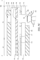
FIGs. 5A to 5C illustrate a method for forming alens hole 550 of anLCD device 500 according to another exemplary embodiment of the present disclosure. - The
LCD device 500 is different from theLCD device 100 in that a measurement pattern has a different configuration. - With reference to
FIG. 5A , the thickness T1 of thearray substrate 110 is measured with aconfocal sensor 555 by using ameasurement pattern 575 disposed on the array substrate 110 (step S510). - The thickness T1 of the
array substrate 110 may be measured with theconfocal sensor 555. To measure the thickness, theconfocal sensor 550 focuses on themeasurement pattern 575 disposed at a position where thelens hole 550 is to be formed. In this manner, the thickness T1 of thearray substrate 110 can be measured more accurately than withoutsuch measurement pattern 575. For example, the measured thickness T1 of thearray substrate 110 may be 250 µm. - With reference to
FIG. 5B , based on the thickness T1 of thearray substrate 110 measured with theconfocal sensor 555, agroove 550a is formed at the position where thelens hole 550 is to be formed with adrill 560 to a particular depth (step S520). - To form the
lens hole 550, thegroove 550a is formed with a thickness that is thinner than the thickness T1 by thedrill 560. If the thickness T1 of thearray substrate 110 is equal to 250 µm, the depth of thegroove 550a drilled by thedrill 560 may be less than 250 µm. Specifically, thegroove 550a may be formed to have a depth of about 95% to 99% of the thickness T1 of thearray substrate 110. For example, the depth of thegroove 550a may be 244 µm, and the thickness T2 of the remaining part of the array substrate may be 6 µm. With reference toFIG. 5C , adhesion force is applied on the area where thegroove 550a is formed with a taping equipment 570 (or other element having adhesive characteristics) to attach the area to aglass core 580, and then theglass core 580 is separated from thearray substrate 110 with thetaping equipment 570 to form the lens hole 550 (S530). That is, atape 585 is pressed by theadhesive taping equipment 570 against the top surface of thegroove 550a formed with thedrill 560, i.e., theglass core 580 so that thetape 585 is attached to theglass core 580. Subsequently, when thetaping equipment 570 pulls down thetape 585 attached to theglass core 580 where thegroove 550a is formed, theglass core 580 can be removed from the array substrate since the thickness T2 is very thin. As a result, thelens hole 550 can be formed. Subsequently, thecamera module 140 is inserted into thearray substrate 110 via thelens hole 550. - According to the above-described method of forming the
lens hole 550, it is not necessary to penetrate thearray substrate 110 with a drill. Accordingly, it is possible to greatly suppress the possibility that glass pieces created by thedrill 560 are introduced between thearray substrate 110 and thecolor filter substrate 120. - The exemplary embodiments of the present disclosure can also be described as follows:
- According to an aspect of the present disclosure, a liquid-crystal display (LCD) device includes: an array substrate on which a sub-pixel is disposed; a color filter substrate on which a color filter corresponding to the sub-pixel is disposed; and a liquid-crystal layer between the array substrate and the color filter substrate. The array substrate comprises a lens hole, the color filter substrate comprises a lens hole guide, and a diameter of the lens hole is smaller than an inner diameter of the lens hole guide.
- The center of the lens hole and a center of the lens hole guide may be configured to be adjacent to each other. An inner edge of the lens hole guide may be spaced apart from an edge of the lens hole.
- The lens hole guide may be configured to surround the lens hole. The lens hole guide may absorb at least some of impact exerted on the array substrate during a process of forming the lens hole.
- The color filter substrate may further include a black matrix. The black matrix may be disposed between the color filter substrate and the lens hole guide and may include an aperture smaller than a diameter of the lens hole, and the center of the aperture and the center of the lens hole guide may be configured to be adjacent to each other.
- The color filter substrate may further include an overcoat layer. The overcoat layer may transmit a visible wavelength band, cover the black matrix and the aperture, and reduce step difference between the black matrix and the aperture.
- The LCD device may further include: a camera module in an area of the array substrate other than the area where the sub-pixels are disposed, and the camera module may include a sensor part and a lens part, the lens part may be inserted into the lens hole and the lens hole guide, and the camera module may capture images via the aperture.
- The LCD device may further include: a first polarization plate disposed under the array substrate; and a second polarization plate disposed on the color filter substrate. The second polarization plate may cover the aperture and comprises a transparent portion in line with the aperture.
- The transmittance of visible light may be higher at the transparent portion than at the remaining portion of the second polarization plate.
- The array substrate may further include a measurement pattern concentric with the lens hole.
- The measurement pattern may be made of a material of a gate line and/or a material of a data line of the array substrate.
- The measurement pattern may have a shape corresponding to the lens hole.
- The inner diameter of the measurement pattern may be larger than the diameter of the lens hole.
- The measurement pattern may be removed during a process of forming the lens hole.
- The measurement pattern may be hidden by the black matrix.
- The measurement pattern may have a circular ring shape or a donut shape.
- According to another aspect of the present disclosure, there is provided a method of fabricating a liquid-crystal display (LCD) device. The method includes: measuring a thickness of an array substrate with a confocal sensor by using a measurement pattern on the array substrate; forming a groove in a position where a lens hole is to be formed to a depth determined based on the thickness of the array substrate measured with the confocal sensor; attaching a glass core to a region where the groove is formed by applying adhesion with a taping equipment, and then separating the glass core from the array substrate with the taping equipment to thereby form the lens hole; and inserting a camera module into the array substrate through the lens hole.
- It will be apparent to those skilled in the art that various modifications and variations can be made in the camera module integrated liquid crystal display device and manufacturing method thereof of the present disclosure without departing from the scope of the invention. Thus, it is intended that the present disclosure cover the modifications and variations of this invention provided they come within the scope of the appended claims and/or their equivalents.
Claims (15)
- A liquid-crystal display device (100) comprising:an array substrate (110) on which a sub-pixel is disposed;a color filter substrate (120) on which a color filter corresponding to the sub-pixel is disposed; anda liquid-crystal layer (115) between the array substrate (110) and the color filter substrate (120),wherein the array substrate (110) comprises a lens hole (150), the color filter substrate (120) comprises a lens hole guide (155), and a diameter of the lens hole (150) is smaller than a diameter of the lens hole guide (155).
- The liquid-crystal display device (100) of claim 1, wherein a center of the lens hole (150) and a center of the lens hole guide (155) are configured to be adjacent to or aligned with each other, and
wherein an inner edge of the lens hole guide (155) is spaced apart from an edge of the lens hole (150). - The liquid-crystal display device (100) of claim 1 or 2, wherein the lens hole guide (155) is configured to surround the lens hole (150) and to absorb at least some pressure exerted on the array substrate (110) during a process of forming the lens hole (150).
- The liquid-crystal display device (100) of any one of claims 1 to 3, wherein the color filter substrate (120) further comprises a black matrix (130), and
wherein the black matrix (130) is disposed between the color filter substrate (120) and the lens hole guide (155) and comprises an aperture (160) smaller than a diameter of the lens hole (150), and a center of the aperture (160) and a center of the lens hole (150) are configured to be adjacent to or aligned with each other. - The liquid-crystal display device (100) of claim 4, wherein the color filter substrate (120) further comprises an overcoat layer (135) disposed above the lens hole guide (155), and
wherein the overcoat layer (135) is configured to pass light of visible wavelength bands, to cover the black matrix (130) and the aperture (160), and to reduce step difference or surface unevenness between the black matrix (130) and the aperture (160). - The liquid-crystal display device (100) of claim 4 or 5, further comprising: a camera module (140) in an area of the array substrate (110) other than the area where the sub-pixels are disposed,
wherein the camera module (140) comprises a sensor part (140b) and a lens part (140a),
the lens part (140a) is accommodated by the lens hole (150) and the lens hole guide (155), and
the camera module (140) is configured to capture images via the aperture (160). - The liquid-crystal display device (100) of any one of claims 1 to 6, further comprising:a first polarization plate (105)under the array substrate (110); anda second polarization plate (125) on the color filter substrate (120),wherein the second polarization plate (125) covers the aperture (160) and comprises a transparent portion (165) in line with the aperture (160).
- The liquid-crystal display device (100) of claim 7, wherein a transmittance of visible light is higher at the transparent portion (165) than at the remaining portion of the second polarization plate (125).
- The liquid-crystal display device (100) of any one of claims 1 to 8, wherein the array substrate (110) further comprises a measurement pattern (175) configured to be concentric with the lens hole (150).
- The liquid-crystal display device (100) of claim 9, wherein the measurement pattern (175) is made of a material of a gate line and/or a material of a data line of the array substrate (110).
- The liquid-crystal display device (100) of claim 9 or 10, wherein the measurement pattern (175) has a shape corresponding to the lens hole (150).
- The liquid-crystal display device (100) of any one of claims 9 to 11, wherein an inner diameter (L3) of the measurement pattern (175) is larger than the diameter of the lens hole (150).
- The liquid-crystal display device of any one of claims 9 to 12, wherein the measurement pattern (175) is hidden by the black matrix (130).
- The liquid-crystal display device (100) of any one of claims 9 to 13, wherein the measurement pattern (175) has a circular ring shape or a donut shape.
- A method of fabricating a liquid-crystal display device (100), the method comprising:measuring a thickness (T1) of an array substrate (110) with a confocal sensor (555) by using a measurement pattern (575) on the array substrate (110);forming a groove (550a) in a position where a lens hole (550) is to be formed to a depth determined based on the thickness (T1) of the array substrate (110) measured with the confocal sensor (555);attaching a glass core (580) to a region where the groove (550a) is formed by applying adhesion with a taping equipment (570), and then separating the glass core (580) from the array substrate (110) with the taping equipment (570) to thereby form the lens hole (550); andinserting a camera module (140) into the array substrate (110) through the lens hole (550).
Priority Applications (1)
| Application Number | Priority Date | Filing Date | Title |
|---|---|---|---|
| EP20185456.9A EP3742222B1 (en) | 2015-12-28 | 2016-11-08 | Camera module integrated liquid crystal display device |
Applications Claiming Priority (1)
| Application Number | Priority Date | Filing Date | Title |
|---|---|---|---|
| KR1020150187173A KR102501111B1 (en) | 2015-12-28 | 2015-12-28 | Camera module integrated liquid display device and manufacturing method thereof |
Related Child Applications (2)
| Application Number | Title | Priority Date | Filing Date |
|---|---|---|---|
| EP20185456.9A Division-Into EP3742222B1 (en) | 2015-12-28 | 2016-11-08 | Camera module integrated liquid crystal display device |
| EP20185456.9A Division EP3742222B1 (en) | 2015-12-28 | 2016-11-08 | Camera module integrated liquid crystal display device |
Publications (2)
| Publication Number | Publication Date |
|---|---|
| EP3187923A1 true EP3187923A1 (en) | 2017-07-05 |
| EP3187923B1 EP3187923B1 (en) | 2020-09-23 |
Family
ID=57391764
Family Applications (2)
| Application Number | Title | Priority Date | Filing Date |
|---|---|---|---|
| EP16197689.9A Active EP3187923B1 (en) | 2015-12-28 | 2016-11-08 | Camera module integrated liquid display device and manufacturing method thereof |
| EP20185456.9A Active EP3742222B1 (en) | 2015-12-28 | 2016-11-08 | Camera module integrated liquid crystal display device |
Family Applications After (1)
| Application Number | Title | Priority Date | Filing Date |
|---|---|---|---|
| EP20185456.9A Active EP3742222B1 (en) | 2015-12-28 | 2016-11-08 | Camera module integrated liquid crystal display device |
Country Status (4)
| Country | Link |
|---|---|
| US (5) | US10334148B2 (en) |
| EP (2) | EP3187923B1 (en) |
| KR (2) | KR102501111B1 (en) |
| CN (2) | CN112612163B (en) |
Cited By (4)
| Publication number | Priority date | Publication date | Assignee | Title |
|---|---|---|---|---|
| EP3627214A1 (en) * | 2018-09-21 | 2020-03-25 | Beijing Xiaomi Mobile Software Co., Ltd. | Electronic device |
| EP3690534A1 (en) * | 2019-01-31 | 2020-08-05 | Beijing Xiaomi Mobile Software Co., Ltd. | Liquid crystal display and terminal |
| EP3690528A1 (en) * | 2019-01-31 | 2020-08-05 | Beijing Xiaomi Mobile Software Co., Ltd. | Liquid crystal display, display method and terminal |
| GB2585692A (en) * | 2019-07-12 | 2021-01-20 | Continental Automotive Gmbh | A method of embedding an imaging device within a display |
Families Citing this family (86)
| Publication number | Priority date | Publication date | Assignee | Title |
|---|---|---|---|---|
| WO2018169102A1 (en) * | 2017-03-14 | 2018-09-20 | 엘지전자 주식회사 | Mobile terminal |
| KR102261212B1 (en) * | 2017-06-09 | 2021-06-03 | 엘지디스플레이 주식회사 | Display device |
| CN107247482B (en) * | 2017-06-27 | 2021-07-16 | 联想(北京)有限公司 | Display and camera integrated device |
| US20190037063A1 (en) * | 2017-07-31 | 2019-01-31 | Guangdong Oppo Mobile Telecommunications Corp., Ltd. | Display panel and electronic device |
| GB2566936A (en) * | 2017-09-20 | 2019-04-03 | Flexenable Ltd | Display device |
| CN110021640B (en) * | 2018-01-08 | 2025-02-11 | 三星显示有限公司 | Electroluminescent device |
| KR102572136B1 (en) | 2018-01-08 | 2023-08-29 | 삼성디스플레이 주식회사 | Electroluminescent device having window |
| KR102443229B1 (en) * | 2018-01-23 | 2022-09-15 | 삼성전자주식회사 | A display comprising an opening for mounting a sensor |
| CN108321163B (en) * | 2018-02-07 | 2020-10-16 | 业成科技(成都)有限公司 | Image capture device and manufacturing method thereof |
| CN108196388B (en) * | 2018-02-12 | 2022-04-19 | 京东方科技集团股份有限公司 | Display device and manufacturing method thereof |
| JP2019158956A (en) * | 2018-03-08 | 2019-09-19 | シャープ株式会社 | Display device |
| KR102560099B1 (en) | 2018-03-30 | 2023-07-26 | 삼성디스플레이 주식회사 | Display device |
| CN108594524B (en) * | 2018-04-26 | 2021-04-13 | 京东方科技集团股份有限公司 | display device |
| JP7182906B2 (en) * | 2018-06-12 | 2022-12-05 | 株式会社ジャパンディスプレイ | Display devices and electronic devices |
| WO2020000187A1 (en) * | 2018-06-26 | 2020-01-02 | Oppo广东移动通信有限公司 | Screen assembly and electronic device |
| CN110646962A (en) * | 2018-06-26 | 2020-01-03 | Oppo广东移动通信有限公司 | Display assembly, electronic device, and manufacturing method of electronic device |
| CN108919545B (en) * | 2018-06-28 | 2021-05-04 | 厦门天马微电子有限公司 | Display panel and display device |
| CN108681150B (en) * | 2018-06-29 | 2023-12-08 | 厦门天马微电子有限公司 | Backlight module and display device |
| CN108957829A (en) * | 2018-07-06 | 2018-12-07 | Oppo广东移动通信有限公司 | Display assembly, electronic device and method for manufacturing electronic device |
| EP3820122B1 (en) * | 2018-07-16 | 2022-02-02 | Guangdong Oppo Mobile Telecommunications Corp., Ltd. | Electronic device |
| CN108897172A (en) * | 2018-07-18 | 2018-11-27 | 深圳市宝明科技股份有限公司 | A kind of backlight with through-hole |
| CN108957855B (en) * | 2018-07-26 | 2021-04-02 | 厦门天马微电子有限公司 | Display device |
| CN108989508B (en) * | 2018-08-24 | 2021-03-26 | Oppo(重庆)智能科技有限公司 | Display screen assembling method, display screen and electronic equipment |
| KR102672833B1 (en) | 2018-08-27 | 2024-06-05 | 엘지디스플레이 주식회사 | Display device |
| CN108828823B (en) * | 2018-08-28 | 2021-06-15 | 厦门天马微电子有限公司 | Display device |
| US11294422B1 (en) | 2018-09-27 | 2022-04-05 | Apple Inc. | Electronic device including a camera disposed behind a display |
| KR102636407B1 (en) * | 2018-09-28 | 2024-02-14 | 엘지디스플레이 주식회사 | Display panel coupled with aligned camera and display device comprising thereof |
| CN109164624B (en) | 2018-09-30 | 2021-08-17 | 京东方科技集团股份有限公司 | Display panel, display device and image acquisition method thereof |
| KR102626939B1 (en) * | 2018-10-05 | 2024-01-19 | 삼성디스플레이 주식회사 | Display device |
| CN109343253A (en) * | 2018-10-30 | 2019-02-15 | 武汉华星光电技术有限公司 | Liquid crystal display panel and preparation method thereof |
| JP7160643B2 (en) * | 2018-11-16 | 2022-10-25 | 株式会社ジャパンディスプレイ | Display device |
| US10845664B2 (en) * | 2018-11-22 | 2020-11-24 | Wuhan China Star Optoelectronics Technology Co., Ltd. | Liquid crystal display panel and terminal device |
| CN111258113A (en) * | 2018-12-03 | 2020-06-09 | 鸿富锦精密工业(深圳)有限公司 | Liquid crystal display device |
| CN110618549B (en) * | 2018-12-03 | 2024-10-29 | 鸿富锦精密工业(深圳)有限公司 | Display device |
| KR102673859B1 (en) | 2018-12-06 | 2024-06-11 | 삼성디스플레이 주식회사 | Display device and electronic device having the same |
| TWI678010B (en) * | 2018-12-07 | 2019-11-21 | 友達光電股份有限公司 | Display array panel and display device |
| CN110888261A (en) * | 2018-12-07 | 2020-03-17 | 鸿富锦精密工业(深圳)有限公司 | Display panel and display device |
| KR102612738B1 (en) * | 2018-12-18 | 2023-12-12 | 엘지디스플레이 주식회사 | Display device |
| KR102680693B1 (en) * | 2018-12-18 | 2024-07-01 | 엘지디스플레이 주식회사 | Display device |
| CN109785744B (en) * | 2018-12-25 | 2023-06-30 | 友达光电(昆山)有限公司 | Display device and terminal using same |
| KR102707679B1 (en) * | 2019-02-13 | 2024-09-19 | 삼성전자주식회사 | Nonvolatile memory device, storage device including nonvolatile memory device, and operating method of nonvolatile memory device |
| KR102611961B1 (en) | 2019-02-26 | 2023-12-11 | 삼성디스플레이 주식회사 | Electronic device |
| JP7257821B2 (en) | 2019-03-11 | 2023-04-14 | 株式会社ジャパンディスプレイ | electro-optical devices and electronics |
| US10866464B2 (en) * | 2019-04-17 | 2020-12-15 | Wuhan China Star Optoelectronics Technology Co., Ltd. | Liquid crystal display panel and electronic device |
| CN109981855A (en) * | 2019-04-26 | 2019-07-05 | 武汉华星光电技术有限公司 | Display device |
| CN111966161B (en) * | 2019-05-20 | 2022-08-05 | 群光电子股份有限公司 | Electronic device and lens module thereof |
| JP7263120B2 (en) * | 2019-05-23 | 2023-04-24 | 株式会社ジャパンディスプレイ | Display device and display panel |
| CN110082937A (en) * | 2019-05-24 | 2019-08-02 | 业成科技(成都)有限公司 | The means of defence of camera aperture |
| US11765945B2 (en) * | 2019-05-27 | 2023-09-19 | Samsung Display Co., Ltd. | Display device having a black matrix |
| CN110275341B (en) * | 2019-06-28 | 2022-04-12 | 厦门天马微电子有限公司 | Display panel and display device |
| KR102890704B1 (en) * | 2019-07-02 | 2025-11-27 | 삼성디스플레이 주식회사 | Electronic apparatus and method of manufacturing the same |
| JP7299092B2 (en) | 2019-07-22 | 2023-06-27 | 株式会社ジャパンディスプレイ | Display device and manufacturing method thereof, electronic device and manufacturing method thereof, and backlight unit |
| CN110471499A (en) * | 2019-07-24 | 2019-11-19 | 武汉华星光电半导体显示技术有限公司 | Display module and display device |
| WO2021021113A1 (en) | 2019-07-29 | 2021-02-04 | Hewlett-Packard Development Company, L.P. | Electronic shutters to enhance privacy |
| CN110473898B (en) * | 2019-07-30 | 2021-10-08 | 武汉华星光电半导体显示技术有限公司 | Organic light emitting diode display panel and method of making the same |
| KR102713286B1 (en) | 2019-09-06 | 2024-10-04 | 삼성전자 주식회사 | Electronic device including camera module |
| CN110716335A (en) * | 2019-09-27 | 2020-01-21 | 武汉华星光电半导体显示技术有限公司 | Display device and method for manufacturing the same |
| CN110764299A (en) * | 2019-10-29 | 2020-02-07 | 深圳市华星光电技术有限公司 | Liquid crystal display panel and display module preparation method |
| CN112736111B (en) * | 2019-10-29 | 2025-08-15 | 北京小米移动软件有限公司 | Screen module and electronic equipment |
| KR102570007B1 (en) | 2019-11-04 | 2023-08-23 | 삼성전자주식회사 | Method and electronic device for correcting handwriting input |
| CN110867136B (en) * | 2019-11-22 | 2021-10-15 | 维沃移动通信有限公司 | Pole screen and electronic equipment |
| CN118765136A (en) | 2019-12-18 | 2024-10-11 | 乐金显示有限公司 | Display device |
| KR102899769B1 (en) * | 2019-12-31 | 2025-12-12 | 엘지디스플레이 주식회사 | Display Panel and Display Device Using the Same |
| KR102830618B1 (en) * | 2019-12-31 | 2025-07-08 | 삼성디스플레이 주식회사 | Display apparatus |
| JP2021139982A (en) * | 2020-03-03 | 2021-09-16 | 日東電工株式会社 | Antiglare film |
| JP2021139981A (en) * | 2020-03-03 | 2021-09-16 | 日東電工株式会社 | Antiglare film |
| KR20210137856A (en) | 2020-05-11 | 2021-11-18 | 삼성전자주식회사 | Electronic device including camera and display |
| KR20210149264A (en) * | 2020-06-01 | 2021-12-09 | 삼성디스플레이 주식회사 | Display device |
| KR20220000440A (en) * | 2020-06-25 | 2022-01-04 | 삼성디스플레이 주식회사 | Display device and method of fabricating the same |
| KR102956966B1 (en) * | 2020-07-21 | 2026-04-24 | 삼성전자 주식회사 | Electronic device including camera device and display |
| CN111726511B (en) * | 2020-07-28 | 2021-09-24 | Oppo广东移动通信有限公司 | Camera decorative piece, its processing method, and electronic equipment |
| KR102841198B1 (en) | 2020-07-31 | 2025-07-31 | 삼성디스플레이 주식회사 | Display device |
| WO2022098058A1 (en) | 2020-11-06 | 2022-05-12 | 삼성전자 주식회사 | Electronic device including display |
| CN114500869B (en) * | 2020-11-13 | 2024-04-05 | 荣耀终端有限公司 | Electronic equipment and under-screen light detection assembly |
| US11706517B2 (en) * | 2021-03-10 | 2023-07-18 | Google Llc | Vertically long apertures for computing device cameras |
| USD962748S1 (en) * | 2021-03-17 | 2022-09-06 | Jinhua Haihua Daily Necessities Factory | Hole locator |
| EP4231611A4 (en) * | 2021-03-26 | 2024-05-29 | Samsung Electronics Co., Ltd. | ELECTRONIC DEVICE COMPRISING A HOUSING COMPRISING A MARK AND METHOD FOR MANUFACTURING SAME |
| US12262600B2 (en) | 2021-03-31 | 2025-03-25 | Chengdu Boe Optoelectronics Technology Co., Ltd. | Display panel, display device, and method for manufacturing a display panel |
| JP2023005488A (en) * | 2021-06-29 | 2023-01-18 | 株式会社ジャパンディスプレイ | Display device |
| US11921368B2 (en) * | 2021-09-22 | 2024-03-05 | Apple Inc. | Electronic devices having antiglare films with transparent apertures |
| US12335422B2 (en) * | 2022-01-10 | 2025-06-17 | Apple Inc. | Handheld electronic device |
| CN115174796B (en) * | 2022-08-30 | 2023-01-31 | 荣耀终端有限公司 | Assembly method, assembly structure and electronic equipment of front camera |
| CN115497391B (en) * | 2022-09-14 | 2026-04-07 | 昆山国显光电有限公司 | Display module and display device |
| CN116073599A (en) * | 2023-01-10 | 2023-05-05 | 河南皓泽电子股份有限公司 | Lens driving mechanism and its base |
| JP2024150288A (en) * | 2023-04-10 | 2024-10-23 | 株式会社ジャパンディスプレイ | camera |
| CN119229739A (en) * | 2023-06-30 | 2024-12-31 | 华为技术有限公司 | Display modules, electronic devices |
Citations (7)
| Publication number | Priority date | Publication date | Assignee | Title |
|---|---|---|---|---|
| US20050264689A1 (en) * | 2004-05-26 | 2005-12-01 | Yang Shou A | Display panel having a video camera |
| US20120069241A1 (en) * | 2010-09-17 | 2012-03-22 | Au Optronics Corporation | Display |
| US20120127487A1 (en) * | 2010-11-18 | 2012-05-24 | Sergey Potapenko | Methods and apparatuses for measuring the thickness of glass substrates |
| KR20120119082A (en) * | 2011-04-20 | 2012-10-30 | 엘지디스플레이 주식회사 | Method of cutting substrate for liquid crystal display devece |
| KR20130027335A (en) * | 2011-09-07 | 2013-03-15 | 엘지디스플레이 주식회사 | Liquid crystal display devece |
| US20130328051A1 (en) * | 2012-06-06 | 2013-12-12 | Jeremy C. Franklin | Notched Display Layers |
| AU2013200511B2 (en) * | 2010-10-29 | 2014-12-11 | Apple Inc. | Camera lens structures and display structures for electronic devices |
Family Cites Families (31)
| Publication number | Priority date | Publication date | Assignee | Title |
|---|---|---|---|---|
| US6844910B2 (en) * | 1999-12-28 | 2005-01-18 | Semiconductor Energy Laboratory Co., Ltd. | Liquid crystal display device and manufacturing method thereof |
| KR101189275B1 (en) * | 2005-08-26 | 2012-10-09 | 삼성디스플레이 주식회사 | Thin film transistor array panel and method for manufacturing the same |
| CN100514109C (en) * | 2007-08-21 | 2009-07-15 | 三星高新电机(天津)有限公司 | Glasses lens plated non-focusing mobile phone camera |
| FI121817B (en) * | 2009-03-18 | 2011-04-29 | Metso Paper Inc | Grinder refiner surface |
| US9131135B2 (en) * | 2009-06-09 | 2015-09-08 | Apple Inc. | Electronic device flash shutter |
| US8456586B2 (en) * | 2009-06-11 | 2013-06-04 | Apple Inc. | Portable computer display structures |
| CN102033409A (en) * | 2009-09-25 | 2011-04-27 | 鸿富锦精密工业(深圳)有限公司 | Portable electronic device |
| KR101646783B1 (en) | 2009-12-08 | 2016-08-08 | 엘지디스플레이 주식회사 | Portable computer |
| TWI462067B (en) * | 2010-04-27 | 2014-11-21 | Lg Display Co Ltd | Display apparatus |
| US9143668B2 (en) * | 2010-10-29 | 2015-09-22 | Apple Inc. | Camera lens structures and display structures for electronic devices |
| KR20120065789A (en) * | 2010-12-13 | 2012-06-21 | 삼성모바일디스플레이주식회사 | Apparatus for organic layer deposition |
| DE102011089443B4 (en) * | 2011-02-14 | 2016-12-01 | Lg Display Co., Ltd. | display device |
| US8567955B2 (en) * | 2011-03-24 | 2013-10-29 | Apple Inc. | Methods and apparatus for concealing sensors and other components of electronic devices |
| JP5066277B1 (en) * | 2011-06-10 | 2012-11-07 | 株式会社東芝 | Television receiver |
| KR101813459B1 (en) * | 2011-06-24 | 2018-01-02 | 엘지디스플레이 주식회사 | Display apparatus |
| JP2013045103A (en) * | 2011-08-26 | 2013-03-04 | Samsung Electronics Co Ltd | Display device |
| US8867015B2 (en) * | 2012-01-11 | 2014-10-21 | Apple Inc. | Displays with liquid crystal shutters |
| KR101406129B1 (en) * | 2012-03-28 | 2014-06-13 | 엘지디스플레이 주식회사 | Display apparatus |
| US9341878B2 (en) * | 2012-04-05 | 2016-05-17 | Apple Inc. | Displays with low reflectance border regions |
| CN102736314B (en) * | 2012-06-29 | 2015-03-25 | 京东方科技集团股份有限公司 | Liquid crystal panel and manufacturing method thereof as well as liquid crystal display |
| KR102006775B1 (en) * | 2012-08-30 | 2019-08-02 | 엘지디스플레이 주식회사 | Liquid crystal panel and liquid crystal display device using the same |
| KR101998096B1 (en) * | 2012-09-03 | 2019-07-09 | 엘지디스플레이 주식회사 | Liquid crystal panel and liquid crystal display device using the same |
| US20140184521A1 (en) * | 2012-12-28 | 2014-07-03 | Wah Yiu Y.U. Kwong | Integrated camera lens and touch screen cover for an electronic device |
| US9806219B2 (en) * | 2013-02-14 | 2017-10-31 | Apple Inc. | Displays with camera window openings |
| JP5923456B2 (en) * | 2013-03-29 | 2016-05-24 | 株式会社ジャパンディスプレイ | Display device |
| WO2015041066A1 (en) * | 2013-09-17 | 2015-03-26 | 株式会社村田製作所 | Camera module, and electronic apparatus |
| CN108663862B (en) * | 2014-02-25 | 2020-02-07 | 群创光电股份有限公司 | Display panel |
| KR102524754B1 (en) * | 2015-09-09 | 2023-04-21 | 엘지디스플레이 주식회사 | Display device |
| CN108427226B (en) * | 2018-05-03 | 2023-04-11 | 京东方科技集团股份有限公司 | Display substrate and display device |
| CN110596939B (en) * | 2019-08-22 | 2021-02-26 | 武汉华星光电技术有限公司 | Display panel and display module |
| JP6807007B1 (en) * | 2019-12-27 | 2021-01-06 | 富士通クライアントコンピューティング株式会社 | Electronics |
-
2015
- 2015-12-28 KR KR1020150187173A patent/KR102501111B1/en active Active
-
2016
- 2016-11-08 EP EP16197689.9A patent/EP3187923B1/en active Active
- 2016-11-08 EP EP20185456.9A patent/EP3742222B1/en active Active
- 2016-11-09 US US15/346,935 patent/US10334148B2/en active Active
- 2016-11-18 CN CN202011549375.5A patent/CN112612163B/en active Active
- 2016-11-18 CN CN201611035761.6A patent/CN106918964B/en active Active
-
2019
- 2019-05-03 US US16/403,081 patent/US10754373B2/en active Active
-
2020
- 2020-07-20 US US16/933,520 patent/US11520374B2/en active Active
-
2022
- 2022-11-04 US US17/981,329 patent/US11921539B2/en active Active
-
2023
- 2023-02-14 KR KR1020230019275A patent/KR102726156B1/en active Active
-
2024
- 2024-02-02 US US18/431,773 patent/US12099380B2/en active Active
Patent Citations (7)
| Publication number | Priority date | Publication date | Assignee | Title |
|---|---|---|---|---|
| US20050264689A1 (en) * | 2004-05-26 | 2005-12-01 | Yang Shou A | Display panel having a video camera |
| US20120069241A1 (en) * | 2010-09-17 | 2012-03-22 | Au Optronics Corporation | Display |
| AU2013200511B2 (en) * | 2010-10-29 | 2014-12-11 | Apple Inc. | Camera lens structures and display structures for electronic devices |
| US20120127487A1 (en) * | 2010-11-18 | 2012-05-24 | Sergey Potapenko | Methods and apparatuses for measuring the thickness of glass substrates |
| KR20120119082A (en) * | 2011-04-20 | 2012-10-30 | 엘지디스플레이 주식회사 | Method of cutting substrate for liquid crystal display devece |
| KR20130027335A (en) * | 2011-09-07 | 2013-03-15 | 엘지디스플레이 주식회사 | Liquid crystal display devece |
| US20130328051A1 (en) * | 2012-06-06 | 2013-12-12 | Jeremy C. Franklin | Notched Display Layers |
Cited By (8)
| Publication number | Priority date | Publication date | Assignee | Title |
|---|---|---|---|---|
| EP3627214A1 (en) * | 2018-09-21 | 2020-03-25 | Beijing Xiaomi Mobile Software Co., Ltd. | Electronic device |
| US10845630B2 (en) | 2018-09-21 | 2020-11-24 | Beijing Xiaomi Mobile Software Co., Ltd. | Electronic device having optical sensor circuit on active display area with modified light guide |
| EP3690534A1 (en) * | 2019-01-31 | 2020-08-05 | Beijing Xiaomi Mobile Software Co., Ltd. | Liquid crystal display and terminal |
| EP3690528A1 (en) * | 2019-01-31 | 2020-08-05 | Beijing Xiaomi Mobile Software Co., Ltd. | Liquid crystal display, display method and terminal |
| US11092830B2 (en) | 2019-01-31 | 2021-08-17 | Beijing Xiaomi Mobile Software Co., Ltd. | Liquid crystal display and terminal |
| US11294226B2 (en) | 2019-01-31 | 2022-04-05 | Beijing Xiaomi Mobile Software Co., Ltd. | Liquid crystal display, display method and terminal |
| GB2585692A (en) * | 2019-07-12 | 2021-01-20 | Continental Automotive Gmbh | A method of embedding an imaging device within a display |
| US12088900B2 (en) | 2019-07-12 | 2024-09-10 | Continental Automotive Gmbh | Method of embedding an imaging device within a display |
Also Published As
| Publication number | Publication date |
|---|---|
| KR20230025423A (en) | 2023-02-21 |
| CN106918964A (en) | 2017-07-04 |
| US10754373B2 (en) | 2020-08-25 |
| US20230059352A1 (en) | 2023-02-23 |
| EP3187923B1 (en) | 2020-09-23 |
| EP3742222A1 (en) | 2020-11-25 |
| US11921539B2 (en) | 2024-03-05 |
| US12099380B2 (en) | 2024-09-24 |
| US20240176388A1 (en) | 2024-05-30 |
| CN112612163A (en) | 2021-04-06 |
| KR102726156B1 (en) | 2024-11-04 |
| KR20170077360A (en) | 2017-07-06 |
| KR102501111B1 (en) | 2023-02-16 |
| US20190260919A1 (en) | 2019-08-22 |
| US20170187934A1 (en) | 2017-06-29 |
| EP3742222B1 (en) | 2022-09-28 |
| CN106918964B (en) | 2021-01-12 |
| US20200348721A1 (en) | 2020-11-05 |
| US11520374B2 (en) | 2022-12-06 |
| US10334148B2 (en) | 2019-06-25 |
| CN112612163B (en) | 2024-12-10 |
Similar Documents
| Publication | Publication Date | Title |
|---|---|---|
| US12099380B2 (en) | Display apparatus comprising a camera module inserted into an opening of an array substrate that is supported by a lens hole guide | |
| US11719962B2 (en) | Display panel substrate defining hole for input image device and liquid crystal display having the same | |
| JP5094250B2 (en) | Display device | |
| US11137635B2 (en) | Display device including an adhesive layer and a non-adhesive layer | |
| KR101291843B1 (en) | Apparatus for inspection of liquid crystal display device and inspecting method thereof | |
| JP5507377B2 (en) | Liquid crystal display | |
| US10705361B2 (en) | Liquid crystal display device | |
| WO2017193442A1 (en) | Lcd display | |
| KR20180026611A (en) | Display apparatus and fabrication method thereof | |
| US20200326583A1 (en) | Display device | |
| US8675155B2 (en) | Liquid crystal display device comprising a first polarizing plate with a cut portion formed directly below a driving chip wherein the cut portion is covered by a bottom surface of a first substrate | |
| JP2010113109A (en) | Method for manufacturing electrooptical device | |
| CN210222403U (en) | Inspection apparatus | |
| CN113009738A (en) | Reflective display screen and reflective display device | |
| KR20150136339A (en) | Array substrate and liquid crystal display device inluding the same | |
| KR20150137278A (en) | Array substrate and liquid crystal display device inluding the same | |
| JP2015022253A (en) | Method for manufacturing substrate for liquid crystal device, substrate for the liquid crystal device, the liquid crystal device, and electronic equipment | |
| KR20050034046A (en) | Light guide plate and the backlight unit for lcd |
Legal Events
| Date | Code | Title | Description |
|---|---|---|---|
| PUAI | Public reference made under article 153(3) epc to a published international application that has entered the european phase |
Free format text: ORIGINAL CODE: 0009012 |
|
| STAA | Information on the status of an ep patent application or granted ep patent |
Free format text: STATUS: REQUEST FOR EXAMINATION WAS MADE |
|
| 17P | Request for examination filed |
Effective date: 20161108 |
|
| AK | Designated contracting states |
Kind code of ref document: A1 Designated state(s): AL AT BE BG CH CY CZ DE DK EE ES FI FR GB GR HR HU IE IS IT LI LT LU LV MC MK MT NL NO PL PT RO RS SE SI SK SM TR |
|
| AX | Request for extension of the european patent |
Extension state: BA ME |
|
| RBV | Designated contracting states (corrected) |
Designated state(s): AL AT BE BG CH CY CZ DE DK EE ES FI FR GB GR HR HU IE IS IT LI LT LU LV MC MK MT NL NO PL PT RO RS SE SI SK SM TR |
|
| GRAJ | Information related to disapproval of communication of intention to grant by the applicant or resumption of examination proceedings by the epo deleted |
Free format text: ORIGINAL CODE: EPIDOSDIGR1 |
|
| GRAP | Despatch of communication of intention to grant a patent |
Free format text: ORIGINAL CODE: EPIDOSNIGR1 |
|
| GRAP | Despatch of communication of intention to grant a patent |
Free format text: ORIGINAL CODE: EPIDOSNIGR1 |
|
| RIC1 | Information provided on ipc code assigned before grant |
Ipc: G06F 1/16 20060101ALI20200203BHEP Ipc: G02F 1/1333 20060101AFI20200203BHEP Ipc: H04N 5/225 20060101ALI20200203BHEP |
|
| STAA | Information on the status of an ep patent application or granted ep patent |
Free format text: STATUS: GRANT OF PATENT IS INTENDED |
|
| RIN1 | Information on inventor provided before grant (corrected) |
Inventor name: KWAK, JINWOOK Inventor name: KIM, JANGCHEOL Inventor name: HONG, JUIK |
|
| INTG | Intention to grant announced |
Effective date: 20200312 |
|
| GRAS | Grant fee paid |
Free format text: ORIGINAL CODE: EPIDOSNIGR3 |
|
| GRAJ | Information related to disapproval of communication of intention to grant by the applicant or resumption of examination proceedings by the epo deleted |
Free format text: ORIGINAL CODE: EPIDOSDIGR1 |
|
| GRAL | Information related to payment of fee for publishing/printing deleted |
Free format text: ORIGINAL CODE: EPIDOSDIGR3 |
|
| STAA | Information on the status of an ep patent application or granted ep patent |
Free format text: STATUS: REQUEST FOR EXAMINATION WAS MADE |
|
| GRAR | Information related to intention to grant a patent recorded |
Free format text: ORIGINAL CODE: EPIDOSNIGR71 |
|
| STAA | Information on the status of an ep patent application or granted ep patent |
Free format text: STATUS: GRANT OF PATENT IS INTENDED |
|
| GRAA | (expected) grant |
Free format text: ORIGINAL CODE: 0009210 |
|
| STAA | Information on the status of an ep patent application or granted ep patent |
Free format text: STATUS: THE PATENT HAS BEEN GRANTED |
|
| INTC | Intention to grant announced (deleted) | ||
| AK | Designated contracting states |
Kind code of ref document: B1 Designated state(s): AL AT BE BG CH CY CZ DE DK EE ES FI FR GB GR HR HU IE IS IT LI LT LU LV MC MK MT NL NO PL PT RO RS SE SI SK SM TR |
|
| INTG | Intention to grant announced |
Effective date: 20200817 |
|
| REG | Reference to a national code |
Ref country code: GB Ref legal event code: FG4D |
|
| REG | Reference to a national code |
Ref country code: CH Ref legal event code: EP |
|
| REG | Reference to a national code |
Ref country code: IE Ref legal event code: FG4D |
|
| REG | Reference to a national code |
Ref country code: DE Ref legal event code: R096 Ref document number: 602016044429 Country of ref document: DE Ref country code: AT Ref legal event code: REF Ref document number: 1316991 Country of ref document: AT Kind code of ref document: T Effective date: 20201015 |
|
| PG25 | Lapsed in a contracting state [announced via postgrant information from national office to epo] |
Ref country code: BG Free format text: LAPSE BECAUSE OF FAILURE TO SUBMIT A TRANSLATION OF THE DESCRIPTION OR TO PAY THE FEE WITHIN THE PRESCRIBED TIME-LIMIT Effective date: 20201223 Ref country code: HR Free format text: LAPSE BECAUSE OF FAILURE TO SUBMIT A TRANSLATION OF THE DESCRIPTION OR TO PAY THE FEE WITHIN THE PRESCRIBED TIME-LIMIT Effective date: 20200923 Ref country code: SE Free format text: LAPSE BECAUSE OF FAILURE TO SUBMIT A TRANSLATION OF THE DESCRIPTION OR TO PAY THE FEE WITHIN THE PRESCRIBED TIME-LIMIT Effective date: 20200923 Ref country code: GR Free format text: LAPSE BECAUSE OF FAILURE TO SUBMIT A TRANSLATION OF THE DESCRIPTION OR TO PAY THE FEE WITHIN THE PRESCRIBED TIME-LIMIT Effective date: 20201224 Ref country code: NO Free format text: LAPSE BECAUSE OF FAILURE TO SUBMIT A TRANSLATION OF THE DESCRIPTION OR TO PAY THE FEE WITHIN THE PRESCRIBED TIME-LIMIT Effective date: 20201223 Ref country code: FI Free format text: LAPSE BECAUSE OF FAILURE TO SUBMIT A TRANSLATION OF THE DESCRIPTION OR TO PAY THE FEE WITHIN THE PRESCRIBED TIME-LIMIT Effective date: 20200923 |
|
| REG | Reference to a national code |
Ref country code: AT Ref legal event code: MK05 Ref document number: 1316991 Country of ref document: AT Kind code of ref document: T Effective date: 20200923 |
|
| PG25 | Lapsed in a contracting state [announced via postgrant information from national office to epo] |
Ref country code: RS Free format text: LAPSE BECAUSE OF FAILURE TO SUBMIT A TRANSLATION OF THE DESCRIPTION OR TO PAY THE FEE WITHIN THE PRESCRIBED TIME-LIMIT Effective date: 20200923 Ref country code: LV Free format text: LAPSE BECAUSE OF FAILURE TO SUBMIT A TRANSLATION OF THE DESCRIPTION OR TO PAY THE FEE WITHIN THE PRESCRIBED TIME-LIMIT Effective date: 20200923 |
|
| REG | Reference to a national code |
Ref country code: NL Ref legal event code: MP Effective date: 20200923 |
|
| REG | Reference to a national code |
Ref country code: LT Ref legal event code: MG4D |
|
| PG25 | Lapsed in a contracting state [announced via postgrant information from national office to epo] |
Ref country code: EE Free format text: LAPSE BECAUSE OF FAILURE TO SUBMIT A TRANSLATION OF THE DESCRIPTION OR TO PAY THE FEE WITHIN THE PRESCRIBED TIME-LIMIT Effective date: 20200923 Ref country code: LT Free format text: LAPSE BECAUSE OF FAILURE TO SUBMIT A TRANSLATION OF THE DESCRIPTION OR TO PAY THE FEE WITHIN THE PRESCRIBED TIME-LIMIT Effective date: 20200923 Ref country code: PT Free format text: LAPSE BECAUSE OF FAILURE TO SUBMIT A TRANSLATION OF THE DESCRIPTION OR TO PAY THE FEE WITHIN THE PRESCRIBED TIME-LIMIT Effective date: 20210125 Ref country code: RO Free format text: LAPSE BECAUSE OF FAILURE TO SUBMIT A TRANSLATION OF THE DESCRIPTION OR TO PAY THE FEE WITHIN THE PRESCRIBED TIME-LIMIT Effective date: 20200923 Ref country code: SM Free format text: LAPSE BECAUSE OF FAILURE TO SUBMIT A TRANSLATION OF THE DESCRIPTION OR TO PAY THE FEE WITHIN THE PRESCRIBED TIME-LIMIT Effective date: 20200923 Ref country code: CZ Free format text: LAPSE BECAUSE OF FAILURE TO SUBMIT A TRANSLATION OF THE DESCRIPTION OR TO PAY THE FEE WITHIN THE PRESCRIBED TIME-LIMIT Effective date: 20200923 |
|
| PG25 | Lapsed in a contracting state [announced via postgrant information from national office to epo] |
Ref country code: ES Free format text: LAPSE BECAUSE OF FAILURE TO SUBMIT A TRANSLATION OF THE DESCRIPTION OR TO PAY THE FEE WITHIN THE PRESCRIBED TIME-LIMIT Effective date: 20200923 Ref country code: AL Free format text: LAPSE BECAUSE OF FAILURE TO SUBMIT A TRANSLATION OF THE DESCRIPTION OR TO PAY THE FEE WITHIN THE PRESCRIBED TIME-LIMIT Effective date: 20200923 Ref country code: AT Free format text: LAPSE BECAUSE OF FAILURE TO SUBMIT A TRANSLATION OF THE DESCRIPTION OR TO PAY THE FEE WITHIN THE PRESCRIBED TIME-LIMIT Effective date: 20200923 Ref country code: IS Free format text: LAPSE BECAUSE OF FAILURE TO SUBMIT A TRANSLATION OF THE DESCRIPTION OR TO PAY THE FEE WITHIN THE PRESCRIBED TIME-LIMIT Effective date: 20210123 Ref country code: PL Free format text: LAPSE BECAUSE OF FAILURE TO SUBMIT A TRANSLATION OF THE DESCRIPTION OR TO PAY THE FEE WITHIN THE PRESCRIBED TIME-LIMIT Effective date: 20200923 |
|
| REG | Reference to a national code |
Ref country code: DE Ref legal event code: R097 Ref document number: 602016044429 Country of ref document: DE |
|
| PG25 | Lapsed in a contracting state [announced via postgrant information from national office to epo] |
Ref country code: SK Free format text: LAPSE BECAUSE OF FAILURE TO SUBMIT A TRANSLATION OF THE DESCRIPTION OR TO PAY THE FEE WITHIN THE PRESCRIBED TIME-LIMIT Effective date: 20200923 Ref country code: MC Free format text: LAPSE BECAUSE OF FAILURE TO SUBMIT A TRANSLATION OF THE DESCRIPTION OR TO PAY THE FEE WITHIN THE PRESCRIBED TIME-LIMIT Effective date: 20200923 |
|
| REG | Reference to a national code |
Ref country code: CH Ref legal event code: PL |
|
| PG25 | Lapsed in a contracting state [announced via postgrant information from national office to epo] |
Ref country code: LU Free format text: LAPSE BECAUSE OF NON-PAYMENT OF DUE FEES Effective date: 20201108 |
|
| PLBE | No opposition filed within time limit |
Free format text: ORIGINAL CODE: 0009261 |
|
| STAA | Information on the status of an ep patent application or granted ep patent |
Free format text: STATUS: NO OPPOSITION FILED WITHIN TIME LIMIT |
|
| REG | Reference to a national code |
Ref country code: BE Ref legal event code: MM Effective date: 20201130 |
|
| PG25 | Lapsed in a contracting state [announced via postgrant information from national office to epo] |
Ref country code: CH Free format text: LAPSE BECAUSE OF NON-PAYMENT OF DUE FEES Effective date: 20201130 Ref country code: DK Free format text: LAPSE BECAUSE OF FAILURE TO SUBMIT A TRANSLATION OF THE DESCRIPTION OR TO PAY THE FEE WITHIN THE PRESCRIBED TIME-LIMIT Effective date: 20200923 Ref country code: SI Free format text: LAPSE BECAUSE OF FAILURE TO SUBMIT A TRANSLATION OF THE DESCRIPTION OR TO PAY THE FEE WITHIN THE PRESCRIBED TIME-LIMIT Effective date: 20200923 Ref country code: LI Free format text: LAPSE BECAUSE OF NON-PAYMENT OF DUE FEES Effective date: 20201130 |
|
| 26N | No opposition filed |
Effective date: 20210624 |
|
| PG25 | Lapsed in a contracting state [announced via postgrant information from national office to epo] |
Ref country code: IE Free format text: LAPSE BECAUSE OF NON-PAYMENT OF DUE FEES Effective date: 20201108 Ref country code: IT Free format text: LAPSE BECAUSE OF FAILURE TO SUBMIT A TRANSLATION OF THE DESCRIPTION OR TO PAY THE FEE WITHIN THE PRESCRIBED TIME-LIMIT Effective date: 20200923 |
|
| PG25 | Lapsed in a contracting state [announced via postgrant information from national office to epo] |
Ref country code: TR Free format text: LAPSE BECAUSE OF FAILURE TO SUBMIT A TRANSLATION OF THE DESCRIPTION OR TO PAY THE FEE WITHIN THE PRESCRIBED TIME-LIMIT Effective date: 20200923 Ref country code: MT Free format text: LAPSE BECAUSE OF FAILURE TO SUBMIT A TRANSLATION OF THE DESCRIPTION OR TO PAY THE FEE WITHIN THE PRESCRIBED TIME-LIMIT Effective date: 20200923 Ref country code: CY Free format text: LAPSE BECAUSE OF FAILURE TO SUBMIT A TRANSLATION OF THE DESCRIPTION OR TO PAY THE FEE WITHIN THE PRESCRIBED TIME-LIMIT Effective date: 20200923 |
|
| PG25 | Lapsed in a contracting state [announced via postgrant information from national office to epo] |
Ref country code: MK Free format text: LAPSE BECAUSE OF FAILURE TO SUBMIT A TRANSLATION OF THE DESCRIPTION OR TO PAY THE FEE WITHIN THE PRESCRIBED TIME-LIMIT Effective date: 20200923 |
|
| PG25 | Lapsed in a contracting state [announced via postgrant information from national office to epo] |
Ref country code: BE Free format text: LAPSE BECAUSE OF NON-PAYMENT OF DUE FEES Effective date: 20201130 |
|
| PG25 | Lapsed in a contracting state [announced via postgrant information from national office to epo] |
Ref country code: NL Free format text: LAPSE BECAUSE OF NON-PAYMENT OF DUE FEES Effective date: 20200923 |
|
| PGFP | Annual fee paid to national office [announced via postgrant information from national office to epo] |
Ref country code: GB Payment date: 20250922 Year of fee payment: 10 |
|
| PGFP | Annual fee paid to national office [announced via postgrant information from national office to epo] |
Ref country code: FR Payment date: 20250925 Year of fee payment: 10 |
|
| PGFP | Annual fee paid to national office [announced via postgrant information from national office to epo] |
Ref country code: DE Payment date: 20250922 Year of fee payment: 10 |