US11137635B2 - Display device including an adhesive layer and a non-adhesive layer - Google Patents
Display device including an adhesive layer and a non-adhesive layer Download PDFInfo
- Publication number
- US11137635B2 US11137635B2 US16/529,958 US201916529958A US11137635B2 US 11137635 B2 US11137635 B2 US 11137635B2 US 201916529958 A US201916529958 A US 201916529958A US 11137635 B2 US11137635 B2 US 11137635B2
- Authority
- US
- United States
- Prior art keywords
- adhesive layer
- display panel
- display
- area
- bend
- Prior art date
- Legal status (The legal status is an assumption and is not a legal conclusion. Google has not performed a legal analysis and makes no representation as to the accuracy of the status listed.)
- Active
Links
Images


Classifications
-
- G—PHYSICS
- G02—OPTICS
- G02F—OPTICAL DEVICES OR ARRANGEMENTS FOR THE CONTROL OF LIGHT BY MODIFICATION OF THE OPTICAL PROPERTIES OF THE MEDIA OF THE ELEMENTS INVOLVED THEREIN; NON-LINEAR OPTICS; FREQUENCY-CHANGING OF LIGHT; OPTICAL LOGIC ELEMENTS; OPTICAL ANALOGUE/DIGITAL CONVERTERS
- G02F1/00—Devices or arrangements for the control of the intensity, colour, phase, polarisation or direction of light arriving from an independent light source, e.g. switching, gating or modulating; Non-linear optics
- G02F1/01—Devices or arrangements for the control of the intensity, colour, phase, polarisation or direction of light arriving from an independent light source, e.g. switching, gating or modulating; Non-linear optics for the control of the intensity, phase, polarisation or colour
- G02F1/13—Devices or arrangements for the control of the intensity, colour, phase, polarisation or direction of light arriving from an independent light source, e.g. switching, gating or modulating; Non-linear optics for the control of the intensity, phase, polarisation or colour based on liquid crystals, e.g. single liquid crystal display cells
- G02F1/133—Constructional arrangements; Operation of liquid crystal cells; Circuit arrangements
- G02F1/1333—Constructional arrangements; Manufacturing methods
- G02F1/1335—Structural association of cells with optical devices, e.g. polarisers or reflectors
- G02F1/133528—Polarisers
-
- G—PHYSICS
- G02—OPTICS
- G02F—OPTICAL DEVICES OR ARRANGEMENTS FOR THE CONTROL OF LIGHT BY MODIFICATION OF THE OPTICAL PROPERTIES OF THE MEDIA OF THE ELEMENTS INVOLVED THEREIN; NON-LINEAR OPTICS; FREQUENCY-CHANGING OF LIGHT; OPTICAL LOGIC ELEMENTS; OPTICAL ANALOGUE/DIGITAL CONVERTERS
- G02F1/00—Devices or arrangements for the control of the intensity, colour, phase, polarisation or direction of light arriving from an independent light source, e.g. switching, gating or modulating; Non-linear optics
- G02F1/01—Devices or arrangements for the control of the intensity, colour, phase, polarisation or direction of light arriving from an independent light source, e.g. switching, gating or modulating; Non-linear optics for the control of the intensity, phase, polarisation or colour
- G02F1/13—Devices or arrangements for the control of the intensity, colour, phase, polarisation or direction of light arriving from an independent light source, e.g. switching, gating or modulating; Non-linear optics for the control of the intensity, phase, polarisation or colour based on liquid crystals, e.g. single liquid crystal display cells
- G02F1/133—Constructional arrangements; Operation of liquid crystal cells; Circuit arrangements
- G02F1/1333—Constructional arrangements; Manufacturing methods
- G02F1/133305—Flexible substrates, e.g. plastics, organic film
-
- G—PHYSICS
- G02—OPTICS
- G02F—OPTICAL DEVICES OR ARRANGEMENTS FOR THE CONTROL OF LIGHT BY MODIFICATION OF THE OPTICAL PROPERTIES OF THE MEDIA OF THE ELEMENTS INVOLVED THEREIN; NON-LINEAR OPTICS; FREQUENCY-CHANGING OF LIGHT; OPTICAL LOGIC ELEMENTS; OPTICAL ANALOGUE/DIGITAL CONVERTERS
- G02F1/00—Devices or arrangements for the control of the intensity, colour, phase, polarisation or direction of light arriving from an independent light source, e.g. switching, gating or modulating; Non-linear optics
- G02F1/01—Devices or arrangements for the control of the intensity, colour, phase, polarisation or direction of light arriving from an independent light source, e.g. switching, gating or modulating; Non-linear optics for the control of the intensity, phase, polarisation or colour
- G02F1/13—Devices or arrangements for the control of the intensity, colour, phase, polarisation or direction of light arriving from an independent light source, e.g. switching, gating or modulating; Non-linear optics for the control of the intensity, phase, polarisation or colour based on liquid crystals, e.g. single liquid crystal display cells
- G02F1/133—Constructional arrangements; Operation of liquid crystal cells; Circuit arrangements
- G02F1/1333—Constructional arrangements; Manufacturing methods
- G02F1/1335—Structural association of cells with optical devices, e.g. polarisers or reflectors
- G02F1/133509—Filters, e.g. light shielding masks
- G02F1/133514—Colour filters
-
- G—PHYSICS
- G02—OPTICS
- G02F—OPTICAL DEVICES OR ARRANGEMENTS FOR THE CONTROL OF LIGHT BY MODIFICATION OF THE OPTICAL PROPERTIES OF THE MEDIA OF THE ELEMENTS INVOLVED THEREIN; NON-LINEAR OPTICS; FREQUENCY-CHANGING OF LIGHT; OPTICAL LOGIC ELEMENTS; OPTICAL ANALOGUE/DIGITAL CONVERTERS
- G02F1/00—Devices or arrangements for the control of the intensity, colour, phase, polarisation or direction of light arriving from an independent light source, e.g. switching, gating or modulating; Non-linear optics
- G02F1/01—Devices or arrangements for the control of the intensity, colour, phase, polarisation or direction of light arriving from an independent light source, e.g. switching, gating or modulating; Non-linear optics for the control of the intensity, phase, polarisation or colour
- G02F1/13—Devices or arrangements for the control of the intensity, colour, phase, polarisation or direction of light arriving from an independent light source, e.g. switching, gating or modulating; Non-linear optics for the control of the intensity, phase, polarisation or colour based on liquid crystals, e.g. single liquid crystal display cells
- G02F1/133—Constructional arrangements; Operation of liquid crystal cells; Circuit arrangements
- G02F1/1333—Constructional arrangements; Manufacturing methods
- G02F1/1343—Electrodes
- G02F1/134309—Electrodes characterised by their geometrical arrangement
-
- G—PHYSICS
- G02—OPTICS
- G02F—OPTICAL DEVICES OR ARRANGEMENTS FOR THE CONTROL OF LIGHT BY MODIFICATION OF THE OPTICAL PROPERTIES OF THE MEDIA OF THE ELEMENTS INVOLVED THEREIN; NON-LINEAR OPTICS; FREQUENCY-CHANGING OF LIGHT; OPTICAL LOGIC ELEMENTS; OPTICAL ANALOGUE/DIGITAL CONVERTERS
- G02F1/00—Devices or arrangements for the control of the intensity, colour, phase, polarisation or direction of light arriving from an independent light source, e.g. switching, gating or modulating; Non-linear optics
- G02F1/01—Devices or arrangements for the control of the intensity, colour, phase, polarisation or direction of light arriving from an independent light source, e.g. switching, gating or modulating; Non-linear optics for the control of the intensity, phase, polarisation or colour
- G02F1/13—Devices or arrangements for the control of the intensity, colour, phase, polarisation or direction of light arriving from an independent light source, e.g. switching, gating or modulating; Non-linear optics for the control of the intensity, phase, polarisation or colour based on liquid crystals, e.g. single liquid crystal display cells
- G02F1/133—Constructional arrangements; Operation of liquid crystal cells; Circuit arrangements
- G02F1/1333—Constructional arrangements; Manufacturing methods
- G02F1/133388—Constructional arrangements; Manufacturing methods with constructional differences between the display region and the peripheral region
-
- G—PHYSICS
- G02—OPTICS
- G02F—OPTICAL DEVICES OR ARRANGEMENTS FOR THE CONTROL OF LIGHT BY MODIFICATION OF THE OPTICAL PROPERTIES OF THE MEDIA OF THE ELEMENTS INVOLVED THEREIN; NON-LINEAR OPTICS; FREQUENCY-CHANGING OF LIGHT; OPTICAL LOGIC ELEMENTS; OPTICAL ANALOGUE/DIGITAL CONVERTERS
- G02F2202/00—Materials and properties
- G02F2202/28—Adhesive materials or arrangements
Definitions
- Embodiments described herein relate generally to a display device.
- Display devices such as liquid crystal displays comprise a polarizer disposed, for example, to cover the display area.
- the polarizer is adhered on the substrate via an adhesive layer.
- an adhesive layer for example, in order to suppress warping of the display panel, which may be caused by contraction of the polarizer, there is a conventionally known technology which forms non-adhesive portions sporadically in the adhesive layer.
- the separator attached on the polarizer is removed to expose the adhesive, and then the polarizer is adhered onto the panel.
- a release-process region where a separator and an adhesive are not attached together is formed in a central portion of the polarizer, thus reducing the removing area of the separator.
- FIG. 1 is a diagram showing a structure and an equivalent circuit of a display device of this embodiment.
- FIG. 2 is a cross section showing a display area of a display panel shown in FIG. 1 .
- FIG. 3 is a cross section of the display panel taken along line A-B shown in FIG. 1 .
- FIG. 4 is a cross section showing a bent region of the display panel shown in FIG. 3 , when it is bent.
- FIG. 5 is a diagram illustrating a step of preparing a non-adhesive layer.
- FIG. 6 is a cross section showing a modified example of the non-adhesive layer.
- FIG. 7 is a cross section showing a modified example of the non-adhesive layer.
- a display device comprises a display panel comprising a display area which displays images, a non-display area surrounding the display area, and a bend area in the non-display area, a first optical film located on the display panel and comprising an end portion which overlaps the bend area, an adhesive layer which adheres the first optical film and the display panel together and a non-adhesive layer located between the first optical film and the display panel, while overlapping the bend area, wherein the non-adhesive layer is in contact with an upper surface of the display panel.
- a display device comprises a display panel which comprises a display area which displays images, a non-display area surrounding the display area, and a bend area in the non-display area, a first optical film located on the display panel and comprising an end portion which overlaps the bend area, an adhesive layer which adheres the first optical film and the display panel together and a non-adhesive layer located between the first optical film and the display panel while overlapping the bend area, wherein the display panel is bent in the bend area, and an end portion of the first optical film is spaced from the display panel in the bend area.
- the display device DSP may be an organic electroluminescent display.
- FIG. 1 is a diagram showing a structure and an equivalent circuit of the display device DSP of the embodiment.
- a first direction X, a second direction Y and a third direction Z are orthogonal to each other, but they may cross each other at an angle other than 90 degrees.
- the first direction X and the second direction Y correspond to a direction parallel to a main surface of the substrate which constitutes display device DSP
- the third direction Z correspond to a thickness direction of the display device DSP.
- a direction towards a tip of an arrow indicating the third direction Z is referred to as above (or, simply, up), and a direction opposite from the tip of the arrow is referred to as below (or, simply, down).
- the display device DSP comprises a display panel PNL, an IC chip 2 and a flexible printed circuit board 3 .
- the display panel PNL is a liquid crystal display panel, and comprises a first substrate SUB 1 , a second substrate SUB 2 , a liquid crystal layer LC, signal lines S, scanning lines G, switching elements SW, pixel electrodes PE, a common electrode CE and the like. Further, the display panel PNL includes a display area DA in which images are displayed and a non-display area NDA which surrounds the display area DA.
- the second substrate SUB 2 opposes the first substrate SUB 1 .
- the first substrate SUB 1 includes a mounting portion MT extending in the first direction X further from the second substrate SUB 2 .
- the first substrate SUB 1 and the second substrate SUB 2 are adhered together a sealing member located (not shown) in the non-display area NDA.
- the display area DA includes a plurality of pixels PX arranged in a matrix disposed along the first direction X and the second direction Y.
- the signal lines S, the scanning lines G, the switching elements SW, the pixel electrodes PE, the common electrode CE and the liquid crystal layer LC are located in the display area DA.
- the signal lines S each extend along the first direction X and the scanning lines G each extend along the second direction Y.
- the switching elements SW are each constituted by a thin-film transistor (TFT), for example, and electrically connected to the respective scanning line G and the respective signal line S.
- the pixel electrodes PE are electrically connected to the switching elements SW, respectively.
- the pixel electrodes PE each oppose the common electrode CE, and drive the liquid crystal layer LC by an electric field produced between the pixel electrodes PE and the common electrode CE.
- a storage capacitor CS is formed, for example, between an electrode at the same potential as that of the common electrode CE and an electrode at the same potential as that of the respective pixel electrode PE.
- the IC chip 2 and the flexible printed circuit substrate 3 are mounted on the mounting portion MA.
- the IC chip 2 may be mounted on the flexible printed circuit substrate 3 .
- the display panel PNL comprises a first edge E 1 and a second edge E 2 , extending along the first direction X, and a third edge E 3 and a fourth edge E 4 extending along the second direction Y.
- the first edge E 1 opposes the second edge E 2 via the display area DA.
- the third edge E 3 opposes the fourth edge E 4 via the display area DA.
- the mounting portion MA is located between the display area DA and the fourth edge E 4 .
- the display panel PNL of this embodiment may be transmissive type which comprises a transmissive display function which displays images by selectively transmitting light from a rear surface side of the first substrate SUB 1 , a reflective type which comprises a reflective display function which displays images by selectively reflecting light from a front surface side of the second substrate SUB 2 , or a trans-reflective type which comprises the transmissive display function and the reflective display function.
- the display panel PNL may comprise a structure provided for a display mode which utilizes a lateral electric field along a main surface of the substrate, a display mode which utilizes a vertical electric field along a normal to the main surface of the substrate, a display mode which utilizes an inclined electric field inclined in an oblique direction with respect to the main surface of the substrate, and further a display mode which utilizes the lateral electric field, the vertical electric field and the inclined electric field in an appropriate combination.
- the main surface of the substrate is a surface parallel to the X-Y plane defined by the first direction X and the second direction Y.
- the display panel PNL of this embodiment is constituted by a flexible substrate and can be bent. Therefore, by bending the display panel PNL in the non-display area NDA, the frame of the display device DSP can be reduced in size.
- the display panel PNL includes a bend area BA 1 in the non-display area NDA on a side of the first edge E 1 .
- the display panel PNL includes a bend area BA 2 in the non-display area NDA on a side of the second edge E 2 . That is, in the display panel PNL illustrated, the bend areas BA 1 and BA 2 are bent such that the first edge E 1 and the second edge E 2 are located under the display area DA.
- the embodiment is not limited to this.
- the display panel PNL is of a rectangular shape whose first edge E 1 and second edges E 2 are long sides, whereas third edges E 3 and fourth edges E 4 are short sides, but it may be of a rectangular shape whose first edge E 1 and second edge E 2 are short sides, whereas third edge E 3 and fourth edge E 4 are long sides.
- FIG. 2 is a cross-section of the display area DA of the display panel PNL shown in FIG. 1 .
- the example illustrated is equivalent to one in which the fringe field switching (FFS) mode, which is one of the display modes which utilizes a lateral electric field, is applied to the display panel PNL.
- FFS fringe field switching
- the first substrate SUB 1 comprises an insulating substrate 10 , insulating films 11 to 13 , signal lines S, a common electrode CE, metallic wiring lines ML, pixel electrodes PE, a first alignment film AL 1 and the like. Note that the switching elements, scanning lines, various insulating films interposed therebetween, and the like are omitted from the illustration in the drawing.
- the insulating substrate 10 is, for example, flexible resin substrate, and is light-transmissive.
- the insulating substrate 10 is formed of, for example, polyimide.
- the insulating film 11 is disposed on the insulating substrate 10 .
- the signal lines S are located on the insulating film 11 , and are covered by the insulating film 12 .
- the insulating film 12 is disposed on the insulating film 11 as well.
- the common electrode CE is located on the insulating film 12 and is covered by the insulating film 13 .
- the common electrode CE is a transparent electrode formed of a transparent conductive material such as indium tin oxide (ITO) or indium zinc oxide (IZO).
- the metallic wiring lines ML are located on common electrode CE such as to be in contact with the common electrode CE.
- the metal lines ML are located directly above the respective signal lines Si.
- the metallic wiring lines ML may be located between the common electrode CE and the insulating film 12 .
- the insulating film 13 covers the metallic wiring lines ML as well.
- the pixel electrodes PE are located on the insulating film 13 , and are covered by the first alignment film AL 1 .
- the pixel electrodes PE each comprise a slit SL at a position opposing to the common electrode CE.
- the pixel electrodes PE are each a transparent electrode formed of a transparent, electrically conductive material such as ITO or IZO.
- the first alignment film AL 1 is disposed on the insulation film 14 as well.
- the insulating films 11 and 13 are each an inorganic insulating films formed from an inorganic insulating material such as a silicon oxide, silicon nitride, and silicon oxynitride, and may be of a single- or multi-layered structure.
- the insulating film 12 is, for example, an organic insulating film formed from an organic insulating material such as an acrylic resin.
- the second substrate SUB 2 comprises an insulating substrate 20 , light-shielding layers BM, color filters CF, an overcoat layer OC and a second alignment film AL 2 etc.
- the insulating substrate 20 is, for example, a flexible resin substrate, and is light-transmissive.
- the insulating substrate 20 is formed of polyimide, for example.
- the light-shielding layers BM and the color filters CF are located on the second insulating substrate 20 on a side opposing the first substrate SUB 1 .
- the light-shielding layers BM each partition each respective pixel and are located directly above the signal lines S, respectively.
- the color filters CF are disposed at positions opposing the respective pixel electrodes PE, and the color filters CF partially overlap the light-shielding layers BM, respectively.
- the color filters CF include a red color filter, a green color filter, a blue color filter and the like.
- the overcoat layer OC covers the color filters CF.
- the overcoat layer OC is formed from a transparent resin material.
- the second alignment film AL 2 covers the overcoat layer OC.
- the first alignment film AL 1 and the second alignment film AL 2 are formed of, for example, a material which exhibits horizontal alignment properties.
- the first substrate SUB 1 and the second substrate SUB 2 described above are disposed such that the first alignment film AL 1 and the second alignment film AL 2 oppose each other.
- the first substrate SUB 1 and the second substrate SUB 2 are adhered together by a sealing member with a predetermined cell gap formed therebetween.
- a liquid crystal layer LC is held on an inner side surrounded by the sealing member, in the cell gap between the first substrate SUB 1 and the second substrate SUB 2 .
- the liquid crystal layer LQ contains liquid crystal molecules LM.
- the liquid crystal layer LC is constituted by a liquid crystal material of a positive type (the dielectric constant anisotropy thereof being positive), or a liquid crystal material of a negative type (the dielectric constant anisotropy thereof being negative).
- a polarizer (a second optical film) PL 1 is located under the display panel PNL such as to overlap the display area DA.
- the polarizer PL 1 is adhered onto the insulating substrate 10 by an adhesive layer GL 1 .
- a polarizer (a first optical film) PL 2 is located above the display panel PNL such as to overlap the display area DA.
- the polarizer PL 2 is adhered onto the insulating substrate 20 by an adhesive layer GL 2 .
- the liquid crystal elements LM are initially aligned along a predetermined direction between the first alignment film AL 1 and the second alignment film AL 2 in an off state, in which an electric field is not formed between the respective pixel electrode PE and the common electrode CE.
- the off state the light irradiated towards the display panel PNL from an illumination unit BL disposed on a rear surface side of the display panel PNL is absorbed by the polarizers PL 1 and PL 2 , thus creating a dark display.
- the liquid crystal elements LM are aligned along a direction different from the direction of the initial alignment, by the electric field, and the direction of alignment is controlled by the electric field.
- the ON state a portion of the light from the illumination unit BL passes through the polarizers PL 1 and PL 2 , thus creating a bright display.
- FIG. 3 is a cross section of the display panel PNL taken along line A-B shown in FIG. 1 .
- FIG. 3 only the main structure of this embodiment is shown and illustration of other members is omitted.
- FIG. 3 shows only the structure on a bend area BA 1 side, but the structure on a bend area BA 2 side is similar to that of the bend area BA 1 side.
- the bend area BA 1 includes bend portions BP 1 and BP 2 .
- the bend portions BP 1 and BP 2 are equivalent to portions formed to have curvature when the bend area BA 1 is bent.
- a portion most close to the display area DA is set as a bending start point P.
- the bending start point P is equivalent to a portion where the bend area BA 1 starts to bend.
- the polarizer PL 1 is not disposed in the bend portions BP 1 and BP 2 .
- the polarizer PL 1 includes a first portion PL 11 , a second portion PL 12 and a third portion PL 13 .
- the first portion PL 11 overlaps the display area DA
- the second portion PL 12 and the third portion PL 13 overlap the non-display area NDA.
- the second portion PL 12 overlaps the bend area BA 1 as well.
- the third portion PL 13 is located on an opposite side to the first portion PL 11 with respect to the bend area BA 1 .
- the bending portion BP 1 is located between the first portion PL 11 and the second portion PL 12 .
- the bend portion BP 2 is located between the second portion PL 12 and the third portion PL 13 .
- a usable example of the method of manufacturing such a polarizer PL 1 is a technique that the polarizer PL 1 is attached onto the display panel PNL, and then the portion of the polarizer PL 1 , which is located in the bend portions BP 1 and BP 2 is remove by laser cutting.
- the first portion PL 11 of the polarizer PL 1 extends to the bending start point P. More specifically, an end portion PLE 1 of the first portion PL 11 overlaps the bending start point P.
- the insulating film 11 which is an inorganic film, is located in the display area DA and extends to the bending start point P. That is, an end portion 11 E of the insulating film 11 is located at the bending start point P.
- the first substrate SUB 1 contains peripheral wiring lines WR in the non-display area NDA. The peripheral wiring lines WR are located on the insulating film 12 .
- the signal lines S and the scanning lines G of the display area DA are relocated in a layer above the insulating film 12 in the non-display area NDA.
- the peripheral wiring lines WR may be located in the same layer as that of the signal lines S and the scanning lines G in the non-display area NDA.
- the peripheral wiring lines WR overlap the bend area BA 1 .
- the sealing member SE is disposed in the position which overlaps the bend area BA 1 .
- the light-shielding layers BM are disposed to cover the non-display area NDA.
- the polarizer PL 2 is disposed in the display area DA to extend to the non-display area NDA. In this embodiment, an end portion PLE of the polarizer PL 22 overlaps the bend area BA 1 .
- the adhesive layer GL 2 adheres the polarizer PL 2 and the display panel PNL together. That is, the adhesive layer GL 2 is in contact with the insulating substrate 20 and the polarizer PL 2 .
- a non-adhesive layer 1 is located to overlap the bend area BA 1 and between the polarizer PL 2 and the display panel PNL.
- the non-adhesive layer 1 is located between the insulating substrate 20 and adhesive layer GL 2 . More specifically, the adhesive layer GL 2 is interposed between the non-adhesive layer 1 and the polarizer PL 2 in a position overlapping the bend area BA 1 .
- the non-adhesive layer 1 is in contact with an upper surface US of the display panel PNL.
- a width of the non-adhesive layer 1 taken along the second direction Y is less than or equal to a width of, for example, the bend portion BP 1 taken along the second direction Y.
- an end portion 1 E of the non-adhesive layer 1 which is on a side of the display area DA, is located on a display area DA side with respect to the end portion PLE 1 of the polarizer PL 1 .
- the non-adhesive layer 1 is formed from, for example, an adhesive whose adhesion degrades by silicone, soot or UV irradiation.
- the non-adhesive layer 1 is formed using silicone, after forming the non-adhesive layer 1 on the insulating substrate 20 , the polarizer PL 2 coated with the adhesive GL 2 is adhered on the display panel PNL.
- the polarizer PL 2 coated with the adhesive GL 2 is adhered on the display panel PNL.
- the adhesive layer GL 2 is interposed between the non-adhesive layer 1 and the polarizer PL 2 .
- the non-adhesive layer 1 is formed using an adhesive those adhesion degrades by UV irradiation
- the non-adhesive layer 1 is formed by the laser beam irradiation onto the adhesive layer GL 2 from above the display panel PNL, and thus the adhesive layer GL 2 is not interposed between the non-adhesive layer 1 and the polarizer PL 2 .
- FIG. 4 is a cross section showing the bend area BA 1 of the display panel shown in FIG. 3 , when bent.
- the bend area BA 1 is bent such that the first portion PL 11 and the third portion PL 13 of the polarizer PL 1 face the third direction Z.
- the illumination unit BL is located between the first portion PL 11 and the third portion PL 13 .
- the bend portions BP 1 and BP 2 are deformed to have curvatures when the bend area BA 1 is bent.
- the display panel PNL does not have curvature. Note that the display panel PNL may have curvature between the bend portion BP 1 and the bend portion BP 2 , but in which case, the second portion PL 12 of the polarizer PL 1 is not provided.
- the bending start point P is located in a boundary between the portion which has the curvature of the display panel PNL and the portion which does not have curvature.
- the position of the bending start point P is defined by the end portion PLE 1 of the polarizer PL 1 and the end portion 11 E of the insulating film 11 . Note that it suffices if the bending start point P is defined by a position which overlaps at least one of the end portions PLE 1 and 11 E, and that is, the other one of the end portions PLE 1 and 11 E needs not to be located on the bending start point P.
- the end portion PLE 2 of the polarizer PL 22 is spaced away from the display panel PNL in the bend area BA 1 . If other words, in the bend area BA 1 , a space is provided between the non-adhesive layer 1 and the insulating substrate 20 . That is, with the non-adhesive layer 1 interposed between the polarizer PL 2 and the display panel PNL, the polarizer PL 2 does not bend to follow the display panel PNL while the display panel PNL is being bent. In the example illustrated, the adhesion between the adhesive layer GL 2 and the non-adhesive layer 1 is greater than the adhesion between the display panel PNL and the non-adhesive layer 1 .
- the non-adhesive layer 1 attaches to the adhesive layer GL 2 in the bend area BA 1 .
- the adhesion between the display panel PNL and the non-adhesive layer 1 should preferably be 500 mN/25 mm or less.
- the adhesion between the display panel PNL and the non-adhesive layer 1 is defined by the adhesion between the insulating substrate 20 and the non-adhesive layer 1 .
- the thickness of the display panel PNL in the bend area BA 1 should preferably be less. Therefore, it is preferable that the polarizer PL 2 should not enter the bend area BA 1 . However, depending on the attachment accuracy of the polarizer PL 2 , the polarizer PL 2 may overlap the bend area BA 1 in some cases as illustrated. If the thickness of the bend area BA 1 increases in this way, it may become undesirably difficult to bend. Moreover, the peripheral wiring lines located in the bend area BA 1 are protected from being broken by controlling the neutral surface. Note here that if the polarizer PL 2 entering the bend area BA 1 is adhered onto the insulating substrate 20 , the neutral surface moves to create a strong stress in the peripheral wiring lines, which may undesirably result in breaking of lines.
- the display panel PNL comprises the non-adhesive layer 1 between the polarizer PL 2 and the insulating substrate 20 in the position which overlaps the bend area.
- the polarizer PL 2 and the insulating substrate 20 do not bond together in the bend area BA 1 .
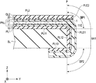
- FIG. 5 is a diagram showing a processing step of manufacturing the non-adhesive layer 1 .
- FIG. 5 shows the processing step in the case where the non-adhesive layer 1 is manufactured using soot.
- part (a) is a cross section
- part (b) is a plan view of the same process as that of part (a).
- the process shown in FIG. 5 is a step of removing the glass substrate GS attached on the display panel PNL after attaching the polarizer PL 1 .
- a region where the non-adhesive layer 1 is to be formed is irradiated with laser LL.
- the region of the insulating substrate 20 where the laser LL is applied, carbonizes to produce soot which gives rises to the non-adhesive layer 1 .
- the first and second edge E 1 and edge E 2 sides are linearly irradiated with the laser LL to form the non-adhesive layer 1 as shown in FIG. 5 , part (b).
- the width of the irradiating portion can be changed.
- the entire display panel PNL is scanned with laser to remove the glass substrate GS from the insulating substrate 20 .
- the adhesive layer GL 2 of the polarizer PL 2 is of a type whose adhesion degrades by UV irradiation
- the non-adhesive layer 1 can be formed using the adhesive layer GL 2 .
- the adhesive layer GL 2 is attached onto the insulating substrate 20 , and then, as shown in FIG. 5 , part (a), the linear region is subjected to UV irradiation.
- FIG. 6 is a cross section showing a modified example of the non-adhesive layer 1 .
- the structure shown in FIG. 6 , part (a) is different from that of FIG. 4 in that the non-adhesive layer 1 is attached to the insulating substrate 20 in the bend area BA 1 .
- the adhesion between the adhesive layer GL 2 and the non-adhesive layer 1 is less than the adhesion between the display panel PNL and the non-adhesive layer 1 . Therefore, the non-adhesive layer 1 is attached to the display panel PNL in the bend area BA 1 .
- the adhesion between the adhesive layer GL 2 and the non-adhesive layer 1 should preferably be 500 mN/25 mm or less.
- part (b) is different from that of FIG. 4 in that the non-adhesive layer 1 is attached to both the adhesive layer GL 2 and the insulating substrate 20 in the bend area BA 1 .
- the adhesion between the adhesive layer GL 2 and the non-adhesive layer 1 is substantially equal to the adhesion between the display panel PNL and the non-adhesive layer 1 .
- FIG. 7 is a cross section showing another modified example of the non-adhesive layer 1 .
- the structure shown in FIG. 7 , part (a) is different from that of FIG. 4 in that adhesive layer GL 2 is not interposed between the non-adhesive layer 1 and the polarizer PL 2 .
- a lower surface PLS of the polarizer PL 2 is in contact with the non-adhesive layer 1 .
- the non-adhesive layer 1 is formed from an adhesive material whose adhesion degrades by UV irradiation
- the lower surface PLS of the polarizer PL 2 is brought into contact with the non-adhesive layer 1 because the non-adhesive layer 1 is formed by UV irradiation carried out from above the display panel PNL.
- the adhesion between the polarizer PL 2 and the non-adhesive layer 1 is greater than the adhesion between the display panel PNL and the non-adhesive layer 1 .
- the non-adhesive layer 1 is attached to the polarizer PL 2 in the bend area BA 1 .
- the adhesion between the display panel PNL and the non-adhesive layer 1 should preferably be 500 mN/25 mm or less.
- part (b) is different from that of FIG. 7 , part (a) in that the non-adhesive layer 1 is attached to the insulating substrate 20 in the bend area BA 1 .
- the adhesion between the polarizer PL 2 and the non-adhesive layer 1 is less than the adhesion between the display panel PNL and the non-adhesive layer 1 . Therefore, the non-adhesive layer 1 is attached to the display panel PNL in the bend area BA 1 .
- the adhesion between the polarizer PL 2 and the non-adhesive layer 1 should preferably be 500 mN/25 mm or less.
- part (c) is different from that of FIG. 7 , part (a) in that the non-adhesive layer 1 is attached to both the polarizer PL 2 and the insulating substrate 20 in the bend area BA 1 .
- the adhesion between the polarizer PL 2 and the non-adhesive layer 1 is substantially equal to the adhesion between the display panel PNL and the non-adhesive layer 1 .
- the embodiment described above is provided in connection with the case where the display device is a liquid crystal display device, but the display device may be an organic electroluminescent display device.
- the polarizer PL 1 is substituted by a support film or the like
- the polarizer PL 2 is substituted by a cover film or the like.
- the illumination unit BL is substituted by a support substrate.
- a display device with which a decrease in production yield is suppressible can be obtained.
Landscapes
- Physics & Mathematics (AREA)
- Nonlinear Science (AREA)
- Mathematical Physics (AREA)
- Chemical & Material Sciences (AREA)
- Crystallography & Structural Chemistry (AREA)
- General Physics & Mathematics (AREA)
- Optics & Photonics (AREA)
- Geometry (AREA)
- Devices For Indicating Variable Information By Combining Individual Elements (AREA)
- Liquid Crystal (AREA)
Abstract
Description
Claims (15)
Applications Claiming Priority (3)
| Application Number | Priority Date | Filing Date | Title |
|---|---|---|---|
| JP2018152338A JP2020027190A (en) | 2018-08-13 | 2018-08-13 | Display device |
| JP2018-152338 | 2018-08-13 | ||
| JPJP2018-152338 | 2018-08-13 |
Publications (2)
| Publication Number | Publication Date |
|---|---|
| US20200050055A1 US20200050055A1 (en) | 2020-02-13 |
| US11137635B2 true US11137635B2 (en) | 2021-10-05 |
Family
ID=69405807
Family Applications (1)
| Application Number | Title | Priority Date | Filing Date |
|---|---|---|---|
| US16/529,958 Active US11137635B2 (en) | 2018-08-13 | 2019-08-02 | Display device including an adhesive layer and a non-adhesive layer |
Country Status (2)
| Country | Link |
|---|---|
| US (1) | US11137635B2 (en) |
| JP (1) | JP2020027190A (en) |
Cited By (1)
| Publication number | Priority date | Publication date | Assignee | Title |
|---|---|---|---|---|
| US12518657B2 (en) * | 2023-01-12 | 2026-01-06 | Samsung Display Co., Ltd. | Display device |
Families Citing this family (7)
| Publication number | Priority date | Publication date | Assignee | Title |
|---|---|---|---|---|
| CN110596971B (en) * | 2019-09-27 | 2022-07-19 | 京东方科技集团股份有限公司 | Display panel, display device and preparation method of display panel |
| WO2022003845A1 (en) * | 2020-07-01 | 2022-01-06 | シャープ株式会社 | Display device and method for manufacturing display device |
| CN113284420B (en) * | 2021-05-26 | 2022-12-06 | 武汉华星光电半导体显示技术有限公司 | display device |
| CN114078394B (en) * | 2021-11-26 | 2023-11-21 | 湖北长江新型显示产业创新中心有限公司 | Display module and foldable display device |
| CN114203050B (en) | 2021-12-28 | 2023-11-28 | 武汉华星光电半导体显示技术有限公司 | Display module and display terminal |
| CN116564185A (en) * | 2022-01-30 | 2023-08-08 | 京东方科技集团股份有限公司 | Display device and display panel |
| US12543490B2 (en) | 2022-06-30 | 2026-02-03 | Chengdu Boe Optoelectronics Technology Co., Ltd. | Display substrate, display module and display device |
Citations (8)
| Publication number | Priority date | Publication date | Assignee | Title |
|---|---|---|---|---|
| JPH1054981A (en) | 1996-08-12 | 1998-02-24 | Matsushita Electric Ind Co Ltd | Polarizer |
| JP2011017970A (en) | 2009-07-10 | 2011-01-27 | Hitachi Displays Ltd | Display device |
| US20110069030A1 (en) * | 2008-03-26 | 2011-03-24 | Kyocera Corporation | Touch Panel and Display Apparatus |
| US20150146386A1 (en) * | 2013-11-28 | 2015-05-28 | Samsung Display Co., Ltd. | Flexible display device |
| CN107065055A (en) * | 2017-01-06 | 2017-08-18 | 芜湖华瀚光电有限公司 | A kind of polaroid and its production technology |
| US20170278899A1 (en) * | 2016-03-25 | 2017-09-28 | Samsung Display Co., Ltd. | Flexible display device |
| US20190072811A1 (en) | 2017-09-05 | 2019-03-07 | Japan Display Inc. | Display device |
| US20190094610A1 (en) | 2017-09-22 | 2019-03-28 | Japan Display Inc. | Display device |
-
2018
- 2018-08-13 JP JP2018152338A patent/JP2020027190A/en active Pending
-
2019
- 2019-08-02 US US16/529,958 patent/US11137635B2/en active Active
Patent Citations (10)
| Publication number | Priority date | Publication date | Assignee | Title |
|---|---|---|---|---|
| JPH1054981A (en) | 1996-08-12 | 1998-02-24 | Matsushita Electric Ind Co Ltd | Polarizer |
| US20110069030A1 (en) * | 2008-03-26 | 2011-03-24 | Kyocera Corporation | Touch Panel and Display Apparatus |
| JP2011017970A (en) | 2009-07-10 | 2011-01-27 | Hitachi Displays Ltd | Display device |
| US20150146386A1 (en) * | 2013-11-28 | 2015-05-28 | Samsung Display Co., Ltd. | Flexible display device |
| US20170278899A1 (en) * | 2016-03-25 | 2017-09-28 | Samsung Display Co., Ltd. | Flexible display device |
| CN107065055A (en) * | 2017-01-06 | 2017-08-18 | 芜湖华瀚光电有限公司 | A kind of polaroid and its production technology |
| US20190072811A1 (en) | 2017-09-05 | 2019-03-07 | Japan Display Inc. | Display device |
| JP2019045763A (en) | 2017-09-05 | 2019-03-22 | 株式会社ジャパンディスプレイ | Display device |
| US20190094610A1 (en) | 2017-09-22 | 2019-03-28 | Japan Display Inc. | Display device |
| JP2019060906A (en) | 2017-09-22 | 2019-04-18 | 株式会社ジャパンディスプレイ | Display device |
Cited By (1)
| Publication number | Priority date | Publication date | Assignee | Title |
|---|---|---|---|---|
| US12518657B2 (en) * | 2023-01-12 | 2026-01-06 | Samsung Display Co., Ltd. | Display device |
Also Published As
| Publication number | Publication date |
|---|---|
| US20200050055A1 (en) | 2020-02-13 |
| JP2020027190A (en) | 2020-02-20 |
Similar Documents
| Publication | Publication Date | Title |
|---|---|---|
| US11137635B2 (en) | Display device including an adhesive layer and a non-adhesive layer | |
| US12259602B2 (en) | Display panel substrate defining hole for input image device and liquid crystal display having the same | |
| US11476283B2 (en) | Display device | |
| US12504662B2 (en) | Display device | |
| US11698561B2 (en) | Display device | |
| US20130335660A1 (en) | Display panel and method of manufacturing the same | |
| US10459265B2 (en) | Display device | |
| US12085825B2 (en) | Display device and touch sensor having plurality of common electrodes | |
| US10816857B2 (en) | Display device | |
| US10859878B2 (en) | Display device | |
| JP2023015123A (en) | semiconductor equipment | |
| US11221526B2 (en) | Display device and substrate comprising organic insulating layer | |
| JP2021131487A (en) | Display device |
Legal Events
| Date | Code | Title | Description |
|---|---|---|---|
| AS | Assignment |
Owner name: JAPAN DISPLAY INC., JAPAN Free format text: ASSIGNMENT OF ASSIGNORS INTEREST;ASSIGNORS:HIGANO, EMI;HIGANO, TOSHIYUKI;ARAKI, SHIGESUMI;SIGNING DATES FROM 20190719 TO 20190722;REEL/FRAME:049940/0168 |
|
| FEPP | Fee payment procedure |
Free format text: ENTITY STATUS SET TO UNDISCOUNTED (ORIGINAL EVENT CODE: BIG.); ENTITY STATUS OF PATENT OWNER: LARGE ENTITY |
|
| STPP | Information on status: patent application and granting procedure in general |
Free format text: DOCKETED NEW CASE - READY FOR EXAMINATION |
|
| STPP | Information on status: patent application and granting procedure in general |
Free format text: NON FINAL ACTION MAILED |
|
| STPP | Information on status: patent application and granting procedure in general |
Free format text: RESPONSE TO NON-FINAL OFFICE ACTION ENTERED AND FORWARDED TO EXAMINER |
|
| STPP | Information on status: patent application and granting procedure in general |
Free format text: NOTICE OF ALLOWANCE MAILED -- APPLICATION RECEIVED IN OFFICE OF PUBLICATIONS |
|
| STPP | Information on status: patent application and granting procedure in general |
Free format text: AWAITING TC RESP., ISSUE FEE NOT PAID |
|
| STPP | Information on status: patent application and granting procedure in general |
Free format text: NOTICE OF ALLOWANCE MAILED -- APPLICATION RECEIVED IN OFFICE OF PUBLICATIONS |
|
| STPP | Information on status: patent application and granting procedure in general |
Free format text: PUBLICATIONS -- ISSUE FEE PAYMENT RECEIVED |
|
| STPP | Information on status: patent application and granting procedure in general |
Free format text: PUBLICATIONS -- ISSUE FEE PAYMENT VERIFIED |
|
| STCF | Information on status: patent grant |
Free format text: PATENTED CASE |
|
| MAFP | Maintenance fee payment |
Free format text: PAYMENT OF MAINTENANCE FEE, 4TH YEAR, LARGE ENTITY (ORIGINAL EVENT CODE: M1551); ENTITY STATUS OF PATENT OWNER: LARGE ENTITY Year of fee payment: 4 |
|
| AS | Assignment |
Owner name: MAGNOLIA WHITE CORPORATION, JAPAN Free format text: ASSIGNMENT OF ASSIGNORS INTEREST;ASSIGNOR:JAPAN DISPLAY INC.;REEL/FRAME:072130/0313 Effective date: 20250625 |