EP3187304A1 - Method and system for convergent polishing - Google Patents
Method and system for convergent polishing Download PDFInfo
- Publication number
- EP3187304A1 EP3187304A1 EP16207175.7A EP16207175A EP3187304A1 EP 3187304 A1 EP3187304 A1 EP 3187304A1 EP 16207175 A EP16207175 A EP 16207175A EP 3187304 A1 EP3187304 A1 EP 3187304A1
- Authority
- EP
- European Patent Office
- Prior art keywords
- polishing
- pitch
- workpiece
- present
- slurry
- Prior art date
- Legal status (The legal status is an assumption and is not a legal conclusion. Google has not performed a legal analysis and makes no representation as to the accuracy of the status listed.)
- Granted
Links
Images









Classifications
-
- B—PERFORMING OPERATIONS; TRANSPORTING
- B24—GRINDING; POLISHING
- B24B—MACHINES, DEVICES, OR PROCESSES FOR GRINDING OR POLISHING; DRESSING OR CONDITIONING OF ABRADING SURFACES; FEEDING OF GRINDING, POLISHING, OR LAPPING AGENTS
- B24B7/00—Machines or devices designed for grinding plane surfaces on work, including polishing plane glass surfaces; Accessories therefor
- B24B7/20—Machines or devices designed for grinding plane surfaces on work, including polishing plane glass surfaces; Accessories therefor characterised by a special design with respect to properties of the material of non-metallic articles to be ground
-
- B—PERFORMING OPERATIONS; TRANSPORTING
- B24—GRINDING; POLISHING
- B24B—MACHINES, DEVICES, OR PROCESSES FOR GRINDING OR POLISHING; DRESSING OR CONDITIONING OF ABRADING SURFACES; FEEDING OF GRINDING, POLISHING, OR LAPPING AGENTS
- B24B37/00—Lapping machines or devices; Accessories
- B24B37/04—Lapping machines or devices; Accessories designed for working plane surfaces
- B24B37/042—Lapping machines or devices; Accessories designed for working plane surfaces operating processes therefor
- B24B37/044—Lapping machines or devices; Accessories designed for working plane surfaces operating processes therefor characterised by the composition of the lapping agent
-
- B—PERFORMING OPERATIONS; TRANSPORTING
- B24—GRINDING; POLISHING
- B24B—MACHINES, DEVICES, OR PROCESSES FOR GRINDING OR POLISHING; DRESSING OR CONDITIONING OF ABRADING SURFACES; FEEDING OF GRINDING, POLISHING, OR LAPPING AGENTS
- B24B13/00—Machines or devices designed for grinding or polishing optical surfaces on lenses or surfaces of similar shape on other work; Accessories therefor
-
- B—PERFORMING OPERATIONS; TRANSPORTING
- B24—GRINDING; POLISHING
- B24B—MACHINES, DEVICES, OR PROCESSES FOR GRINDING OR POLISHING; DRESSING OR CONDITIONING OF ABRADING SURFACES; FEEDING OF GRINDING, POLISHING, OR LAPPING AGENTS
- B24B13/00—Machines or devices designed for grinding or polishing optical surfaces on lenses or surfaces of similar shape on other work; Accessories therefor
- B24B13/005—Blocking means, chucks or the like; Alignment devices
-
- B—PERFORMING OPERATIONS; TRANSPORTING
- B24—GRINDING; POLISHING
- B24B—MACHINES, DEVICES, OR PROCESSES FOR GRINDING OR POLISHING; DRESSING OR CONDITIONING OF ABRADING SURFACES; FEEDING OF GRINDING, POLISHING, OR LAPPING AGENTS
- B24B37/00—Lapping machines or devices; Accessories
- B24B37/04—Lapping machines or devices; Accessories designed for working plane surfaces
- B24B37/07—Lapping machines or devices; Accessories designed for working plane surfaces characterised by the movement of the work or lapping tool
- B24B37/10—Lapping machines or devices; Accessories designed for working plane surfaces characterised by the movement of the work or lapping tool for single side lapping
- B24B37/102—Lapping machines or devices; Accessories designed for working plane surfaces characterised by the movement of the work or lapping tool for single side lapping the workpieces or work carriers being able to rotate freely due to a frictional contact with the lapping tool
-
- B—PERFORMING OPERATIONS; TRANSPORTING
- B24—GRINDING; POLISHING
- B24B—MACHINES, DEVICES, OR PROCESSES FOR GRINDING OR POLISHING; DRESSING OR CONDITIONING OF ABRADING SURFACES; FEEDING OF GRINDING, POLISHING, OR LAPPING AGENTS
- B24B37/00—Lapping machines or devices; Accessories
- B24B37/34—Accessories
-
- B—PERFORMING OPERATIONS; TRANSPORTING
- B24—GRINDING; POLISHING
- B24B—MACHINES, DEVICES, OR PROCESSES FOR GRINDING OR POLISHING; DRESSING OR CONDITIONING OF ABRADING SURFACES; FEEDING OF GRINDING, POLISHING, OR LAPPING AGENTS
- B24B41/00—Component parts such as frames, beds, carriages, headstocks
- B24B41/06—Work supports, e.g. adjustable steadies
- B24B41/067—Work supports, e.g. adjustable steadies radially supporting workpieces
-
- B—PERFORMING OPERATIONS; TRANSPORTING
- B24—GRINDING; POLISHING
- B24B—MACHINES, DEVICES, OR PROCESSES FOR GRINDING OR POLISHING; DRESSING OR CONDITIONING OF ABRADING SURFACES; FEEDING OF GRINDING, POLISHING, OR LAPPING AGENTS
- B24B57/00—Devices for feeding, applying, grading or recovering grinding, polishing or lapping agents
- B24B57/02—Devices for feeding, applying, grading or recovering grinding, polishing or lapping agents for feeding of fluid, sprayed, pulverised, or liquefied grinding, polishing or lapping agents
-
- B—PERFORMING OPERATIONS; TRANSPORTING
- B24—GRINDING; POLISHING
- B24B—MACHINES, DEVICES, OR PROCESSES FOR GRINDING OR POLISHING; DRESSING OR CONDITIONING OF ABRADING SURFACES; FEEDING OF GRINDING, POLISHING, OR LAPPING AGENTS
- B24B7/00—Machines or devices designed for grinding plane surfaces on work, including polishing plane glass surfaces; Accessories therefor
- B24B7/04—Machines or devices designed for grinding plane surfaces on work, including polishing plane glass surfaces; Accessories therefor involving a rotary work-table
Definitions
- optical fabrication processes typically include 1) shaping, 2) grinding, 3) edge grinding/polishing, 4) full aperture intermediate polishing or lapping, 4) full aperture final polish, and 5) small tool polishing.
- Significant advances in precision optical fabrication have been made since the invention of the laser, when the demand for high optical quality material including precise surface figure rose dramatically.
- optical fabrication is an art rather than a technology.
- significant progress has been made in the ability to deterministically remove material during the grinding process based on advancements in tooling and real time diagnostics using Computer Numerical Controlled (CNC) grinders.
- CNC Computer Numerical Controlled
- MRF Magnetorheological Finishing
- embodiments of the present invention relate to deterministic polishing of optical elements in as little as a single iteration.
- the invention has been applied to the single iteration polishing of an optical element under a fixed set of polishing parameters regardless of the initial shape of the element.
- the methods and systems described herein are applicable to the processing and fabrication of a wide variety of optical materials suitable for use with high power laser and amplifier systems.
- Scratches on the surface of high value optics used in high-peak-power laser systems are known to lead to laser damage initiation.
- Much effort has been employed over the years to reduce the number and size of scratches formed during optical fabrication. Scratches are caused, for example, by sliding rogue particles or asperities that are under load on the surface of the optic during cleaning, polishing, and handling.
- Previous work to reduce rogue particles involved modifying and retrofitting existing full aperture polishers. This method was sufficient for dealing with foreign rogue particles leading to scratching.
- Current mitigation strategies are largely limited to cleanliness practices during polishing.
- a second limitation in control of rogue particles is the limited understanding and control of the particle size distribution of the slurry during the polishing process.
- the current state of technology is limited to using un-optimized, poorly understood filtration techniques.
- Embodiments of the present invention reduce rogue particle introduction during polishing by implementing one or more of the following steps: 1) creating a full polishing system that ensures that no rogue particles enter the workpiece-lap interface by hermetically sealing the polisher to prevent drying of the slurry; 2) providing a 100% humidity environment in order to prevent dried slurry agglomeration which can act as rogue particles; 3) using chemically stabilized polishing slurries that minimize within slurry particle agglomeration; and 4) using optimized filtration constantly removing any created rogue particles in the polishing system.
- a polishing system for polishing an optical element includes a polishing pad having a radial dimension and a septum disposed on the polishing pad and configured to partially surround the optical element.
- the optical element contacts the polishing pad over a range of the radial dimension and a pad wear rate of the polishing pad is substantially constant as a function of radial dimension over the range of the radial dimension.
- a high humidity polishing system includes a polishing unit including a polishing pad and a slurry delivery system operable to provide a slurry to the polishing pad.
- the high humidity polishing system also includes an enclosure surrounding the polishing unit. A humidity inside the enclosure is sufficient to prevent substantial drying of the slurry.
- a slurry system for polishing an optical element includes a solvent and an abrasive component supported in the solvent.
- the slurry system also includes a surfactant supported in the solvent.
- a method of mounting a workpiece to a substrate includes determining a peak-to-valley height value and determining a value related to pitch area.
- the method also includes computing a relative area of pitch, computing a button radius, and computing a number of pitch buttons.
- the method further includes coupling N pitch buttons to the workpiece and coupling the N pitch buttons to the substrate.
- Embodiments of the present invention provide an apparatus and method for polishing flat and spherical round and rectangular surfaces on glass of various aspect ratios (diameter/thickness).
- Polishing systems provided by embodiments of the present invention, which can be referred to as a Convergent, Initial surface independent, Single iteration, Rogue-particle free (CISR) polisher, provide one or more of the following characteristics:
- embodiments of the present invention provide methods and systems suitable for polishing optics to a predetermined shape in a single iteration.
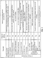
- FIG. 1 is a chart illustrating parameters impacting polishing non-uniformity according to an embodiment of the present invention.
- Embodiments of the present invention provide techniques and systems to mitigate polishing non-uniformity. Control of some of the parameters illustrated in FIG. 1 are described in more detail in U.S. Patent Application No. 12,695/986, filed on January 28, 2010 , the disclosure of which is hereby incorporated by reference in its entirety.
- a mirror septum is utilized in embodiments of the present invention to reduce the elastic lap response (4.2) and the viscoelastic effect (4.5) and to provide a constant lap wear (4.6.1).
- the optic shape is then used to drive the polishing process to convergence (4.6.4).
- the various parameters have been reduced or eliminated except for a single variable, which is then used to converge to the desired shape for the optical element in a full aperture polishing system.
- the parameters affecting material removal illustrated in FIG. 1 only one variable is left, the mismatch between the optic and the lap. Using a lap with the shape that you want the optical element to eventually take, the optic element is then polished in a convergent manner to match the shape of the lap.
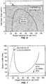
- FIG. 2A is a simplified plot illustrating peak-to-valley heights as a function of polishing time for different polishing configurations according to an embodiment of the present invention.
- a plot of the peak-to-valley height of the optical element as a function of time of polishing is illustrated for various polishing configurations.
- optical elements can be polished with little to no change in the peak-to-valley height as a function of polishing time.
- the "Pad wear reduced" curve (#5) the inventors have determined that as you polish, the pad changes shape and as a result that shape changes the pressure distribution on the optical element as you polish.
- Embodiments of the present invention therefore, use a septum to contact the lap and achieve essentially the opposite wear (i.e., spatially) that the optical element is producing, thereby counterbalancing the pad wear to produce spatially uniform pad wear.
- embodiments of the present invention provide for reduction in the viscoelastic effect as illustrated in curve #6, producing a substantially flat peak-to-valley height as a function of time.
- FIGS. 2B-2G illustrate different polishing configurations according to an embodiment of the present invention.
- the parameters illustrated in FIGS. 2B-2G are matched to the curve numbers in FIG. 2A .
- FIG. 2A illustrates stable peak-to-valley heights for plot #6 (Viscoelastic reduce (77)), at times longer than 100 hours, the peak-to-valley height can increase to higher levels, increasing the peak-to-valley height as a function of time.
- FIG. 2H is a simplified plot illustrating peak-to-valley heights as a function of polishing time for a polishing configuration according to an embodiment of the present invention. As illustrated in FIG. 2H , the convergence point is migrating in the time period between 0 hours and ⁇ 150 hours.
- the inventors believe that one mechanism potentially responsible for the migration of the convergence point is that the balance between the pad wear caused by the optical element and the pad wear caused by the septum is disturbed, resulting in the increase in peak-to-valley height.
- Embodiments of the present invention adjust the convergence point by removing the optical element being polished and operating the polishing system with only the septum. By running the system with only the septum, the convergence point is adjusted to return the peak-to-valley height to a value less than a predetermined level. Because the migration of the convergence point occurs over a period longer than the period associated with a polishing operation for a single optical element. As an example, a polishing time for a particular optical element may be 10 hours, with numerous (e.g., 15 optical elements) being polished in the ⁇ 150 hour period illustrated in FIG. 2H prior to the peak-to-valley height increasing above 2.5 ⁇ m.
- the adjustment of the convergence point is therefore provided over a long-term time period in comparison to the time period typically utilized to polish a single optical element.
- Embodiments of the present invention are not limited to adjustment of the convergence point over such a long-term time period, but the following example is presented in terms of a time period associated with polishing processes for multiple optical elements.
- the convergence point initially migrated to from about 0.5 ⁇ m to about 2.5 ⁇ m during the first 150 hours of polishing.
- embodiments of the present invention remove the optical element in order to operate the polishing system using only the septum for a period of time in order to reduce the peak-to-valley height to a predetermined level.
- operation of the polishing system using only the 0.6 psi septum during the period from ⁇ 200 hours to ⁇ 400 hours reduces the convergence point as illustrated by the peak-to-valley height dropping to 0.48 mm.
- both a septum and an optical element are utilized, which results in a renewed drift in the convergence point during the period from ⁇ 400 hours to ⁇ 500 hours.
- polishing using the septum only after ⁇ 500 hours produces a reduction in the convergence point as expected.
- embodiments utilize a process in which polishing of a septum (e.g., a 0.6 psi septum) without the use of an optical element as a method to fine tune the convergence point.
- FIG. 17 is a simplified flowchart illustrating a method of polishing a set of optical elements according to an embodiment of the present invention.
- the method 1700 includes polishing a first subset of the optical elements using a septum and a polishing process characterized by a peak-to-valley height less than a first predetermined value (1710).
- the method also includes determining that the peak-to-valley height is greater than or equal to the first predetermined value (1712). Once the peak-to-valley height reaches the first predetermined value, the last optical element of the first subset optical elements is removed and the polishing system is operated with no optical element for a period of time (1714).
- the second predetermined value is less than the first predetermined value. In other embodiments, the second predetermined value is equal to the first predetermined value.
- operation of the polishing system during the adjustment of the convergence point utilizes the septum without an optical element, one of the optical elements (as discussed in the alternative embodiment below), a device other than the septum or an optical element, or the like.
- shapes other than the septum that adjust the convergence point are included within the scope of the present invention.
- a second subset of the optical elements is polished using the septum and the polishing process characterized by a peak-to-valley height less than the first predetermined value (1718).
- the method illustrated in FIG. 17 can be modified to remove the septum and polish one of the optical elements in the set of optical elements or a dummy optical element without the use of the septum, thereby modifying process 1714.
- the peak-to-valley height increasing in a negative direction can be adjusted using this complementary correction method.
- FIG. 3A is a simplified plot illustrating polishing convergence for varying initial shapes according to an embodiment of the present invention.
- the optical element was a low aspect ratio round workpiece.
- the peak-to-valley variation in the workpiece i.e., the optical element
- the peak-to-valley variation in the workpiece is originally about 7 ⁇ m for Experiment 79 (i.e., about 14 waves) and is reduced to about -1 ⁇ m (i.e., about 2 waves).
- the original peak-to-valley variation is about -7 ⁇ m and is reduced to about -1.5 ⁇ m.
- embodiments of the present invention provide a convergent polishing technique that results in optical polishing that converges to a uniform smoothness independent of the original variations in the optical element.
- the current convergence band illustrated in FIG. 3A is characterized by a peak-to-valley variation less about 0.5 ⁇ m wide and negative, the present invention is not limited to this particular variation and other bands with narrower variation centered at zero are included within the scope of the present invention.
- figure convergence is driven by the mismatch between the lap and the optic shape, enabling a single iteration, initial-surface-independent polishing process.
- the optic will converge to the same figure as the lap due to the optic-lap mismatch normalization of pressure.
- embodiments of the present invention provide for convergence of the polishing process to a band characterized by a predetermined peak-to-valley height, with the peak-to-valley height remaining in the band for extended periods of time.
- the convergent polishing process terminates at a constant peak-to-valley variation and stays at this convergent value for an extended period of time.
- the convergent polishing technique is self-terminating in a single iteration, providing the desired shape based on the shape of the lap independent of the initial surface of the optical element.
- FIG. 3B is a simplified plot illustrating polishing convergence for a low aspect ratio round optical element according to an embodiment of the present invention.
- the polishing pad utilized in the polishing process illustrated in FIG. 3B i.e., an IC1000TM polishing pad available from Dow Chemical Company of Midland, MI
- the polishing pad utilized in the polishing process illustrated in FIG. 3A i.e., a SubaTM 550 polishing pad available from Dow Chemical Company.
- FIG. 3C is a simplified plot illustrating polishing convergence for a square optical element according to an embodiment of the present invention.
- FIG. 3D is a simplified plot illustrating polishing convergence for a round, high aspect ratio optical element according to an embodiment of the present invention.
- the peak-to-valley height converges to a predetermined band as a function of polishing time for workpieces with different initial surface figures and for four different configurations.
- a low aspect ratio square workpiece was polished using an IC1000TM polishing pad
- a high aspect ratio round (ground or polished) workpiece was polished using an IC1000TM polishing pad.
- the workpieces which were characterized by varying initial surface figure, were polished identically, with all of the workpieces converging to a final, nominally flat shape, thus demonstrating convergent full aperture polishing.
- FIGS. 4A-4E are surface contours illustrating peak-to-valley height at various polishing times according to an embodiment of the present invention.
- the original surface is illustrated in FIG. 4A , with a peak-to-valley height variation (PV) of 6.5 ⁇ m.
- the convergent polishing process terminates at a fixed PV after a predetermined period of time.
- FIG. 5A is a simplified perspective illustration of a polishing septum according to an embodiment of the present invention.
- the septum 500 in the embodiment illustrated in FIG. 5A includes a curve 510 shaped to receive a round optical element.
- the septum which can be a sacrificial workpiece that also results in pad wear that counteracts the spatially non-uniform pad wear caused by the optical element being polished) is modified to receive optical elements, which may be referred to as workpieces, that have different shapes, including square optics, rectangular optics, or the like.
- the septum 500 can include a stack of materials as illustrated in FIG.
- a structural layer 520 formed, for example, from 25 mm of stainless steel or other materials with sufficient rigidity and density, a compliance layer 522 formed, for example, from 3 mm of rubber or other compliant material, and a polishing layer 524 formed, for example, from 1.1 mm of fused silica or other material comparable to the optical element being polished.
- the materials utilized in the various layers can be modified to provide the functions of rigidity/mass, compliance, and polishing similarity.
- the structural layer could be formed from aluminum or other material that is dense, including laminated materials, to preferably provide a low aspect ratio for the septum.
- the septum illustrated in FIG. 5A is suitable for polishing of a circular optical elements, other shapes including square and rectangular optical elements are included within the scope of the present invention.
- the septum thus provides a flat shape due to the compliance layer that enables normalization of the pressure to a uniform pressure across the septum as applied to the pad.
- Materials of than rubber for example, a soft polymer, foam, silicones, combinations thereof, or the like, could be utilized.
- the compliance layer can be bonded to the structural layer using epoxies or other adhesives as needed.
- the use of the same material for the polishing layer as the optic being polished is useful in providing the same pad wear rate, but other materials can be utilized as appropriate to the particular application.
- the use of a material that is different from the optic being polished will result in a different septum shape as will be evident to one of skill in the art. In the septum design illustrated in FIG.
- the pressure (i.e., the load) on lap resulting from the septum i.e., 0.3 psi
- the pressure from the optic i.e., the load
- the septum i.e., 0.3 psi
- a different septum shape is produced by specifying a different pressure between the septum and the optic.
- FIG. 6 is a simplified plot of pad wear rate as a function of radial distance according to an embodiment of the present invention.
- the wear due to the workpiece i.e., the wear rate of the polishing pad
- the area crosshatched to the right is a function of the distance from the center of the polisher. This area under the curve illustrates how much the pad is going to wear if you just put the optical element on the lapping pad.
- the optical element also referred to as an optic
- the optical element is positioned at a location 25 mm from the center of the polisher with a diameter of 100 mm.
- the polishing pad wear resulting from the septum (illustrated as complimentary wear by the area crosshatched to the left), is provided to produce an overall pad wear rate that is constant as a function of distance (C).
- C distance
- f o r 2 a sin ⁇ 1 x r r ⁇ r .
- the septums provided by embodiments of the present invention, as illustrated in FIG. 5A provide benefits not available using conventional polishing techniques.
- the shape of the septum is designed, using the Preston equation as described in relation to FIGS. 6 and 7 , to provide for a uniform pad wear rate as a function of position across the optic.
- the uniformity of pad wear is characterized by a pad wear rate value differing less than 5% over the portion of the pad in contact with the optical element.
- the pad wear rate value differs less than 2%, less than 1.5%, less than 1%, less than 0.75%, less than 0.5%, less than 0.4%, less than 0.3%, less than 0.3%, less than 0.2%, less than 0.1%, less than 0.05%, less than 0.025%, or less than 0.01%.
- a first pad wear rate as a function of position is associated with the wear due to the optical element and a second pad wear rate as a function of position is associated with the septum (see FIG. 6 ). The sum of these pad wear rates provides a substantially uniform rate at portions of the pad that are in contact with the optical element.
- the pad wear rate uniformity extends to portions of the pad not in contact with the optical element (e.g., at radial distances less than 25 mm and greater than 125 mm in FIG. 6 ) as appropriate to the particular application, although the uniformity may decrease in these regions.
- the optical element e.g., at radial distances less than 25 mm and greater than 125 mm in FIG. 6 .
- septums as described herein may also have other mutual benefits in addition to improving spatial pad wear uniformity, due to other phenomena that scale linearly with velocity and pressure. Some examples of such phenomena include pad compression and viscoelasticity, pad glazing, friction-induced temperature effects, slurry distribution, and the like.
- the pad wear as a function of position is substantially uniform as a function of position, for example, less than several waves for optical elements.
- the pad wear uniformity is within a wave over the radial distance in contact with the optical element, although the uniformity may be characterized by even more uniform pad wear, for example, less than a wave.
- FIG. 7 is a simplified plot of septum width as a function of radial distance according to an embodiment of the present invention.
- the septum width in FIG. 7 i.e., a circumferential width
- the septum width in FIG. 7 is bounded by the maximum thickness set by the circumference of the lap at the particular radial distance (there is only so much circumference available to cover with the septum at small radial distances) and the minimum thickness set by the viscoelastic and the rigid punch effect.
- the viscoelastic effect is more prominent, whereas for harder pads, the rigid punch effect is more prominent.
- the shape of the septum is determined for a circular optic, but other shapes for the optical element are included within the scope of the present invention.
- the loading of the septum can be different from the loading of the optic, for example, even a non-uniform loading.
- the function f o (s) can be calculated for a given shape, for example, a circular or rectangular optic, and then put into this formula to define the septum shape.
- the functions f o (r) and f s (r), called circumferential widths here, are defined as the fraction of the lap circumference at radius r that is covered by the optic or septum, respectively.
- the constant value illustrated in FIG. 6 may not be achievable since the radial velocity tends toward zero as the radial distance decreases.
- the optic is located a finite distance from the center (e.g., 25 mm in the illustrated embodiment)
- this design constraint is met by the septum designs described herein. Because the optic does not overlap with radial distances less than 25 mm, a design flexibility for the constant pad wear rate is provided at radial distances not overlapping with the optic.
- FIGS. 8A-8C are simplified plots of septum load as a function of radial distance according to an embodiment of the present invention.
- Embodiments of the present invention can utilize septums that uniformly loaded ( FIG. 8A ), differentially loaded ( FIG. 8B ), or continuously loaded ( FIG. 8C ).
- the plots in FIGS. 8A-8C illustrate that, as discussed in relation to the pad wear rate, the load ( ⁇ ( r )) can be a function of position.
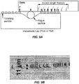
- FIG. 9A is a simplified schematic diagram illustrating scratching by rogue particles.
- stringent requirements can be placed on the scratch density.
- the inventors believe that some scratches are caused during polishing by rogue particles, which are particles larger than other particles present in the polishing slurry, for example, either a foreign particle or particles with a particle size distribution larger than the average particle size of the other particles in the slurry.
- the rogue particles produce a higher load on the optic and produce a scratch or a series of scratches.
- FIG. 9B is an image illustrating scratching by rogue particles.
- an additional source producing rogue particles is the drying of the slurry.
- an additional source producing rogue particles is the drying of the slurry.
- the slurry dry out, but it chemically reacts with itself to produce, from a soft agglomerate, a hard agglomerate upon drying.
- the agglomerates can then produce scratches as illustrated in FIG. 9B .
- Embodiments of the present invention prevent drying of the slurry by enclosing the polishing system, which prevents foreign particles from entering, but also provides a high humidity environment so the slurry is prevented from drying out.
- a rinsing system can be used to rinse the optic when removed from the system to prevent slurry from remaining on the optic.
- the rinsed optic can be dried after removal without the drying of the slurry, which was removed during the rinsing process.
- system components can be coated with a fluorinated polymer layer to reduce the adhesion between the slurry and the various system components.
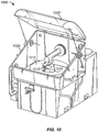
- FIG. 10 is a simplified perspective diagram of a high humidity polishing system according to an embodiment of the present invention.
- the high humidity polishing system 1000 includes a polishing surface 1010, which can be a polishing pad, and an optic 1012 partially surrounded by a septum 1014.
- a moveable cover 1020 is able to be positioned in contact with an enclosure 1022 to form a controlled environment surrounding the polishing surface.
- Inputs and output ports for polishing slurry (not shown) and an input port 1030 and an output port 1032 for a humid gas (e.g., water vapor) are provided as part of the system.
- a humid gas e.g., water vapor
- the humidity inside the polishing system is higher than the ambient humidity, for example, higher than 80%, higher than 85%, higher than 90%, higher than 95%, higher than 97%, higher than 98%, higher than 99% and up to 100%.
- the humidity is provided at a high level to prevent substantial drying of the slurry in the system. The lack of drying in the environment prevents the formation of the hard agglomerates and the associated scratching.
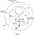
- FIG. 11 is a simplified plan view of a portion of a high humidity polishing system differing in some respects from the high humidity polishing system illustrated in FIG. 10 .
- an optic 1105 is placed on a lap 1110 and spatially controlled using guide wheels.
- a different septum design is used in which a mirror septum 1120 is provided to produce uniform pad wear.
- a 100% humidity feed port 1030 is provided adjacent the lap 1110 so that the polishing environment can provide the desired controlled high humidity atmosphere in a manner similar to a sealed chamber (e.g., a hermetic chamber 1107).
- a sealed chamber e.g., a hermetic chamber 1107
- FIG. 12 illustrates plots of normalized interface height for polishing solutions at a range of dilutions as a function of time according to an embodiment of the present invention.
- the normalized interface height as a function of time provides insight into the settling properties of the illustrates slurries since the interface between the slurry and the solvent separating out of the slurry decreases in height as the slurry settles to the bottom of the container (e.g., a graduated cylinder).
- Hastilite PO mixed at a 1:4 ratio with DI water settles most quickly, with the normalized interface height dropping to 30% within about 25 minutes.
- a 1:1 dilution of Hastilite PO and DI water increases the settling time by an order of magnitude, with a 30% normalized interface height being reached in about 300 minutes.
- the undiluted Hastilite PO provides the longest settling time, dropping to around 60% at 300 minutes. Therefore, the dilution of the slurry, for example, Hastilite PO, impacts the settling time.
- FIG. 13 illustrates plots of normalized interface height for polishing solutions under the influence of agitation according to an embodiment of the present invention. As illustrated in FIG. 13 , agitation produces negligible differences in the settling times for the slurry diluted in either DI water or tap water.
- FIG. 14 illustrates plots of normalized interface height for polishing solutions as a function of time according to an embodiment of the present invention.
- the slurry illustrated in FIG. 14 is Hastilite PO, but other slurries are included within the scope of the present invention.
- Hastilite PO diluted to Baume 9 squares is characterized by the fastest settling time, dropping to 10% of the original normalized interface height in a period of about 30 minutes.
- the neat formulation of Hastilite PO provides an increased settling time in a manner similar to the dilution effects illustrated in FIG. 12 .
- Addition of an additive to prevent agglomeration provides the greatest settling times as illustrated by Hastilite PO diluted to Baume 9 with 1% volume of the surfactant ⁇ -90 (diamonds).
- the addition of the surfactant increases the settling time to provide a normalized interface height of almost 90% of the original height at 800 minutes.
- Exemplary anionic surfactants in addition to ⁇ -90 include Alkyl sulfates (e.g., Sodium dodecyl sulfate, ammonium lauryl sulfate, or the like); Alkyl sulfonates (e.g., Dodecyl benzene sulfonic acid, Sulfonic 100, Calimulse EM-99, or the like); Alkyl ether phosphates (e.g., Triton H66, Triton QS44, or the like); Alkyl carboxylates (e.g. Sodium stearate or the like), or other suitable anionic surfactants.
- Alkyl sulfates e.g., Sodium dodecyl sulfate, ammonium lauryl sulfate, or the like
- Alkyl sulfonates e.g., Dodecyl benzene sulfonic acid, Sulfonic 100
- the surfactant which can be used as an additive to the polishing slurry can include sodium, ammonium, or potassium salts in which the counterion is not active.
- the inventors have determined that the stabilization of the slurry by the surfactant (at an appropriate pH in some embodiments) provides for improved polishing results.
- Embodiments of the present invention are not limited to the use of anionic surfactants, but can also use cationic surfactants.
- exemplary cationic surfactants include Trimethylalkylammonium chlorides (e.g. cetyl trimethylammonium bromide (CTAB), distearyl dimethyl ammonium chloride, or the like); Benzalkonium chlorides; Alkylpyridinium chlorides (e.g. Cetyl pyridinium chloride); or other suitable cationic surfactants.
- CTAB cetyl trimethylammonium bromide
- Benzalkonium chlorides e.g. cetyl trimethylammonium bromide (CTAB), distearyl dimethyl ammonium chloride, or the like
- Benzalkonium chlorides e.g. cetyl trimethylammonium bromide (CTAB), distearyl dimethyl ammonium chloride, or the like
- Benzalkonium chlorides e.g. cetyl trimethyl
- the surfactant is effective to separate the polishing by-products from optical element undergoing polishing.
- the presence of the by-product can reduce the stability of the polishing slurry.
- the surfactant is effective to prevent the agglomeration of the by-products, thereby increasing the long-term stability of the polishing slurry.
- by-products are cations (such as K+, Na+, Ca2+, Mg2+, etc) from the polished away glass during polishing.
- the water used to prepare the slurry may contain varying concentrations of metallic cations.
- cations such as Na+, B3+, Fe2+, Ca2+, Mg2+, and Al3+ are released into the slurry as by-products of the polishing process. The presence of these ions has the potential to reduce stabilizer efficacy by disrupting the electrostatic interaction between the slurry particles and stabilizer molecules.
- Chelation agents e.g., glycine, citric acid, ethylenediaminetetraacetic acid (EDTA), or the like
- EDTA ethylenediaminetetraacetic acid
- the addition of a chelation agent to the slurry may both improve initial stabilization efficiency and may prolong its stability as polishing by-products accumulate.
- embodiments of the present invention utilize chelation agents to improve slurry stabilization.
- FIG. 15 is a simplified plot of relative interface height for stabilized and unstabilized polishing solutions as a function of time according to an embodiment of the present invention. As illustrated in FIG. 15 , the stabilization of the slurry by, for example, the addition of the anionic surfactant additive, produces significant increases in settling time.
- FIG. 16 is a polishing solution volume for stabilized and unstabilized polishing solutions as a function of particle size according to an embodiment of the present invention.
- the addition of the additive to the slurry results in a reduction in the particle sizes in the slurry.
- the particle size distribution for the stabilized slurry is characterized by the majority of the particles being less than 1 ⁇ m in size, with a peak of the distribution at about 0.25 ⁇ m.
- the peak of the distribution is centered at about 1 ⁇ m with either half or the majority of particles being characterized by the larger particle size distribution.
- the stabilized slurry results in an improved polishing outcome because the smaller particle size distribution provides smaller slurry particles during the polishing process.
- the inventors have demonstrated that the addition of the additive provides a slurry that is still characterized by an acceptable material removal rate and improved micro-roughness.
- the inventors have determined that in some optical finishing operations utilizing grinding followed by polishing of thin optical elements, stress is introduced by the grinding operation, resulting in a tendency of the optical element to bend in response to the grinding induced stress.
- the optical element is chemically etched to remove surface layers, thereby reducing the stress present in the optical element.
- the optical element can be exposed to an acid or other suitable etchant (e.g., immersed in an acid bath) after grinding to remove a predetermined surface region of the optical element.
- an optical element characterized by a first bend curvature is ground. After grinding, the optical element is characterized by a second bend curvature greater than the first bend curvature. In some embodiments, the increase in bend curvature results from stress introduced into the workpiece during the grinding process.
- the optical element is chemically etched to remove a predetermined portion of the optical element. After chemical etching, the optical element is characterized by a third bend curvature less than the second bend curvature. In some embodiments, the third bend curvature is less than or equal to the first bend curvature, returning the optical element to the curvature characterizing the optical element before the beginning of the finishing process.
- the chemical etching process reduces the stress introduced during grinding in some embodiments.
- FIGS. 18A-18C are images illustrating surface curvature before grinding, after grinding, and after chemical etching according to an embodiment of the present invention.
- the surface curvature prior to grinding is characterized by a peak-to-valley value of 1.29 ⁇ m.
- the surface curvature after grinding is characterized by a peak-to-valley value of 3.65 ⁇ m as illustrated in FIG. 18B .
- Embodiments of the present invention utilize chemical etching of the ground surface to remove residual stress present after the grinding process to return the figure to approximately the original shape as shown in FIG.
- embodiments of the present invention provide methods and systems in which chemical etching is a useful mitigation technique to reduce or eliminate residual stress contributing to optic/lap mismatch.
- PBB pitch button bonding
- ⁇ PV optical element
- PBB includes a mounting technique that uses small islands of pitch between the workpiece and the mount that are cooled from the softening temperature of the pitch. At room temperature, the workpiece-pitch button-mount system is stiff, and the workpiece largely maintains its initial surface figure.
- the workpiece After polishing using PBB techniques, the workpiece converges to the shape of the lap because, without limiting embodiments of the present invention, of the lack of workpiece bending and a dominance of the workpiece-lap mismatch due to the workpiece shape effect on the pressure distribution.
- an optical element e.g., a fused silica or phosphate glass optic
- a substrate e.g., a stainless steel blank
- pitch buttons The geometry of the pitch buttons, as described more fully below, prevents the deflection of the workpiece due to differences in coefficients of thermal expansion between the workpiece and the substrate.
- isothermal cooling is utilized to reduce or eliminate deflection of the workpiece.
- FIGS. 19A-19F are simplified schematic diagrams illustrating a method of performing pitch button bonding according to an embodiment of the present invention.
- an adhesion/protection layer that increases adhesion between the glass-pitch interface and protects the glass surface from staining due to the pitch contact, residual slurry making contact, and the like) is applied to surface S2 of the workpiece and the reflected wavefront is measured through surface S1.
- the adhesion/protection layer is a tape in some embodiments and the tape is optional in some embodiments.
- Pitch buttons are applied to the surface of the tape (or surface S2 of the workpiece) as illustrated in FIG. 19B .
- the application of the pitch buttons is performed in light of several variables including the pitch type, the radius (r p ) of the pitch buttons, the thickness (tp) of the pitch buttons, the spacing (s) between pitch buttons, and the like.
- the pitch buttons are annealed (e.g., in an oven) using, for example, heating elements, as illustrated in FIG. 19C .
- the temperature of the annealing process which may vary as a function of time, is selected to bring the whole system (e.g., glass, block, & pitch) to an elevated temperature near the temperature of the pitch at which the pitch starts to undergo significant stress relaxation (referred to as Tg) of the pitch and then cool the system as isothermally as possible to prevent or reduce the impact of residual stresses deforming the workpiece shape.
- FIG. 19D illustrates attachment of the workpiece with annealed pitch buttons to a preheated substrate (e.g., an aluminum or stainless steel block) with sufficient rigidity and mechanical properties for use during a polishing operation. Shims of a predetermined thickness (e.g., 1.25 mm) may be used during the mounting of the workpiece to the substrate. The mounted structure is then centered on the substrate, cooled, for example, using air cooling, and the shims are removed as illustrated in FIG. 19E . To characterize the optical properties of the workpiece after mounting, the reflected wavefront can be measured through surface S1 as illustrated in FIG. 19F .
- a preheated substrate e.g., an aluminum or stainless steel block
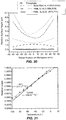
- FIG. 20 is a plot illustrating the measured change in surface figure of fused silica and phosphate glass in various PPB configurations according to an embodiment of the present invention.
- the changes in surface figure of fused silica (FS) and phosphate glass (PG) optical elements for three conditions are shown.
- the workpieces used in the measurements shown in FIG. 20 were 100 mm in diameter with a thickness of 2.2 mm.
- the relative surface height (FS) varies from about 7.5 ⁇ m at peripheral portions to about 3.7 ⁇ m at central portions and from about 10.1 ⁇ m to about 4.2 ⁇ m for PG.
- FIG. 21 is a plot of measured thermal expansion of pitches according to an embodiment of the present invention.
- the thermal expansion of two pitches (Blocking Pitch-1 Black, available from Universal Photonics and Cycad Blackgold optical polishing pitch available from Cycad Products) as measured using a thermal-mechanical analysis, is illustrated.
- the pitches increase in dimension, with a measured coefficient of thermal expansion of 37 x 10 -6 °C -1 for BP1 and 43 x 10 -6 °C -1 for Cycad.
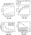
- FIG. 22A is a plot of workpiece peak-to-valley (PV) height as a function of undercooling of pitch for a single button and three buttons according to an embodiment of the present invention.
- PV peak-to-valley
- the use of multiple pitch buttons significantly reduced the workpiece PV height.
- FIG. 22B is a plot of workpiece peak-to-valley height as a function of pitch button radius according to an embodiment of the present invention.
- FIG. 22C is a plot of normalized workpiece peak-to-valley height as a function of pitch button offset according to an embodiment of the present invention.
- the PV height after PBB is normalized in FIG. 22C by dividing it by the relative total button area in microns and plotted as a function of the separation distance between buttons (d m ), measured in millimeters for 3 button and 9 button cases.
- the size of the pitch buttons are varied from 10 mm radius to 20 mm radius.
- the curve in FIG. 22C represents an empirical curve fit to the computed data.
- FIG. 22D is a plot ofworkpiece peak-to-valley height as a function of relative total pitch button area according to an embodiment of the present invention.
- FIG. 22D illustrates 3 and 9 button cases after PPB in which the spacing between buttons is kept at a value greater than 20 mm.
- the line in FIG. 22D represents an empirical curve fit to the computed data.
- FIG. 23 is a simplified schematic diagram illustrating pitch button bonding parameters according to an embodiment of the present invention.
- the PBB parameters include the modulus (E p and E w ), coefficient of thermal expansion ( ⁇ p and ⁇ w ), and the thickness (t p and t w ) of both the pitch buttons and the workpiece, respectively.
- the PBB parameters also include the radius of the pitch buttons (r p ), the radius of the workpiece (r w ), the center to center separation between pitch buttons (s), and the spacing between pitch buttons (d m ).
- the total number of pitch buttons is indicated by N.
- the pitch buttons can have uniform dimensions or varying dimensions as appropriate to the particular application. Thus, both material and geometric parameters are utilized in the methods and systems described herein.
- FIGS. 24A and 24B are drawings illustrating optimized pitch button bonding patterns for optical elements according to an embodiment of the present invention.
- an optimized PBB pattern is illustrated for a 100 mm diameter fused silica workpiece (i.e., Samples S18-S20).
- an optimized PBB patter is illustrated for a 100 mm diameter phosphate glass workpiece (Samples P1-P2).
- FIG. 25A is a plot of workpiece peak-to-valley height as a function of spacing between buttons according to an embodiment of the present invention.
- FIG. 25A illustrates the change in surface figure of a fused silica workpiece (i.e., 100 mm diameter x 2.2 mm thick FS optical element) in various PPB configurations using pitch materials as a function of button spacing (d m ).
- FIG. 25B is a plot of workpiece peak-to-valley height as a function of area fraction according to an embodiment of the present invention.
- FIG. 26 is a simplified flowchart illustrating a method of determining pitch button bonding parameters according to an embodiment of the present invention.
- the method includes determining a peak-to-valley (PV) height value (2610) and determining a value related to pitch area (2612).
- the PV height value can be a minimum acceptable PV height measured in terms of dimensions (e.g., 0.05 ⁇ m) or in terms of the wavelength of light transmitted by the optical element (e.g., ⁇ /10).
- a r PV s C .
- the method additionally includes computing the number of pitch buttons (N) (2618), which may be evenly spaced.
- N pitch buttons are then applied to the workpiece (2620) in accordance with the parameters computed using the method in order to couple the pitch buttons to the workpiece.
- the pitch buttons can be applied to an adhesive and/or protective material such as a tape or other suitable material coupled to the workpiece.
- the workpiece is then mounted to a substrate, e.g., an optical flat comprising stainless steel, aluminum, combinations thereof, or the like, by coupling the N pitch buttons to the substrate (2622).
- FIG. 26 provides a particular method of determining pitch button bonding parameters according to an embodiment of the present invention. Other sequences of steps may also be performed according to alternative embodiments. For example, alternative embodiments of the present invention may perform the steps outlined above in a different order. Moreover, the individual steps illustrated in FIG. 26 may include multiple sub-steps that may be performed in various sequences as appropriate to the individual step. Furthermore, additional steps may be added or removed depending on the particular applications.
- One of ordinary skill in the art would recognize many variations, modifications, and alternatives.
Landscapes
- Engineering & Computer Science (AREA)
- Mechanical Engineering (AREA)
- Finish Polishing, Edge Sharpening, And Grinding By Specific Grinding Devices (AREA)
- Manufacture Of Macromolecular Shaped Articles (AREA)
- Mechanical Treatment Of Semiconductor (AREA)
Abstract
Description
- This application claims priority to
U.S. Provisional Patent Application No. 61/454,893, filed on March 21, 1011 - The United States Government has rights in this invention pursuant to Contract No. DE-AC52-07NA27344 between the U.S. Department of Energy and Lawrence Livermore National Security, LLC, for the operation of Lawrence Livermore National Laboratory.
- Conventional optical fabrication processes typically include 1) shaping, 2) grinding, 3) edge grinding/polishing, 4) full aperture intermediate polishing or lapping, 4) full aperture final polish, and 5) small tool polishing. Significant advances in precision optical fabrication have been made since the invention of the laser, when the demand for high optical quality material including precise surface figure rose dramatically. However, as generally practiced today, optical fabrication is an art rather than a technology. In recent decades, significant progress has been made in the ability to deterministically remove material during the grinding process based on advancements in tooling and real time diagnostics using Computer Numerical Controlled (CNC) grinders. Similarly, the advent of small tool polishing (e.g., computer controlled optical polishers (CCOS)) and Magnetorheological Finishing (MRF) has revolutionized the polishing industry. However, full aperture lap polishing, which is still the most commonly used and typically the most economical method for polishing glass and silicon wafers, does not provide a deterministic process. Although incremental improvements have been made, conventional polishing still requires highly skilled opticians using artisan techniques. This type of polishing typically requires multiple iterative cycles involving polishing, measuring, and adjusting parameters to converge to the desired surface figure (i.e. flatness or conformance to a specified radius). Thus, there is a need in the art for improved methods and systems related to the polishing of optical elements.
- According to the present invention, techniques related to optical systems are provided. More particularly, embodiments of the present invention relate to deterministic polishing of optical elements in as little as a single iteration. Merely by way of example, the invention has been applied to the single iteration polishing of an optical element under a fixed set of polishing parameters regardless of the initial shape of the element. The methods and systems described herein are applicable to the processing and fabrication of a wide variety of optical materials suitable for use with high power laser and amplifier systems.
- According to another embodiment of the present invention, methods and systems related to surface fracture "free" finishing are provided. Scratches on the surface of high value optics used in high-peak-power laser systems are known to lead to laser damage initiation. Hence, much effort has been employed over the years to reduce the number and size of scratches formed during optical fabrication. Scratches are caused, for example, by sliding rogue particles or asperities that are under load on the surface of the optic during cleaning, polishing, and handling. Previous work to reduce rogue particles involved modifying and retrofitting existing full aperture polishers. This method was sufficient for dealing with foreign rogue particles leading to scratching. Current mitigation strategies are largely limited to cleanliness practices during polishing. This strategy, however, is highly sensitive to the degree of cleanliness practice, operator skill set, and complexity of the polisher. Additionally, these strategies are difficult to implement with high efficiency. A second limitation in control of rogue particles is the limited understanding and control of the particle size distribution of the slurry during the polishing process. The current state of technology is limited to using un-optimized, poorly understood filtration techniques.
- Embodiments of the present invention reduce rogue particle introduction during polishing by implementing one or more of the following steps: 1) creating a full polishing system that ensures that no rogue particles enter the workpiece-lap interface by hermetically sealing the polisher to prevent drying of the slurry; 2) providing a 100% humidity environment in order to prevent dried slurry agglomeration which can act as rogue particles; 3) using chemically stabilized polishing slurries that minimize within slurry particle agglomeration; and 4) using optimized filtration constantly removing any created rogue particles in the polishing system.
- According to an embodiment of the present invention, a polishing system for polishing an optical element is provided. The polishing system includes a polishing pad having a radial dimension and a septum disposed on the polishing pad and configured to partially surround the optical element. The optical element contacts the polishing pad over a range of the radial dimension and a pad wear rate of the polishing pad is substantially constant as a function of radial dimension over the range of the radial dimension.
- According to another embodiment of the present invention, a high humidity polishing system is provided. The high humidity polishing system includes a polishing unit including a polishing pad and a slurry delivery system operable to provide a slurry to the polishing pad. The high humidity polishing system also includes an enclosure surrounding the polishing unit. A humidity inside the enclosure is sufficient to prevent substantial drying of the slurry.
- According to a specific embodiment of the present invention, a slurry system for polishing an optical element is provided. The slurry system includes a solvent and an abrasive component supported in the solvent. The slurry system also includes a surfactant supported in the solvent.
- According to another specific embodiment of the present invention, a method of mounting a workpiece to a substrate is provided. The method includes determining a peak-to-valley height value and determining a value related to pitch area. The method also includes computing a relative area of pitch, computing a button radius, and computing a number of pitch buttons. The method further includes coupling N pitch buttons to the workpiece and coupling the N pitch buttons to the substrate.
- Embodiments of the present invention provide an apparatus and method for polishing flat and spherical round and rectangular surfaces on glass of various aspect ratios (diameter/thickness). Polishing systems provided by embodiments of the present invention, which can be referred to as a Convergent, Initial surface independent, Single iteration, Rogue-particle free (CISR) polisher, provide one or more of the following characteristics:
- 1) polishing parameters are fixed (i.e. not variable) and the same during/between polishing runs regardless of the initial surface figure of the workpiece;
- 2) polishing can be done in a single iteration from the ground state since the workpiece figure will converge to the desired shape matching that of the lap; and
- 3) polishing is performed in a rogue particle-'free' environment leading to little or no scratching on the workpiece.
- 4) polishing is performed using highly controlled particle size distribution using chemical stabilization and/or engineered filtration system.
- Embodiments of the present invention rely on one or more of the following principles to achieve the desired polishing process:
- 1) essentially all factors contributing to non-uniform spatial material removal on the optic are eliminated except for optic-lap mismatch (i.e. physical non-uniform separation between optic and lap) which leads to convergence of the optic surface figure to desired shape (i.e., the shape of the lap); and
- 2) the sources of entry and creation of rogue particles into/in the polisher system have been removed or are actively removed which leads little/no scratching of the workpiece.
- As described more fully throughout the present specification, engineering features provided by embodiments of the present invention may include one or more of the following:
- 1) using specially designed septum(s) for round and rectangular workpieces to counteract non-uniform pad wear;
- 2) using a specially designed septum to counteract viscoelastic induced non-uniform stress distribution and non-uniform material removal;
- 3) using a specially design septum to ensure uniform distribution of slurry to the workpiece;
- 4) using a rectangular shaped septum of glass base to provide stability in uniform pad wear;
- 5) using a rectangular shaped septum of CVO diamond base for conditioning pad ensuring constant material removal rate with polishing time;
- 6) using a wheel driven workpiece to prevent moment force contributions to non-uniform stress distribution and non-uniform material removal;
- 7) using low-z pivot point mounting to minimize moment forces on workpiece and septums;
- 8) using kinematics (motion of workpiece and lap) to cause uniform time average velocity on the workpiece preventing non-uniform material removal due to kinematics;
- 9) using a chemically stabilized polishing slurry (e.g., use an anionic (for example, micro-90) or cationic surfactant plus a chelator at appropriate pH & concentration in cerium oxide (Hastilite PO) slurry) to minimize particle agglomeration (a source of rogue particles);
- 10) using a 100% humidity hermetically sealed polishing chamber to: a) prevent the creation of dried polishing slurry, which is known to result in scratch-causing rogue-particles and b) prevent foreign rogue particles in the environment from entering into the polishing system;
- 11) using a stiff button bonding technique (also called pitch button bonding (PBB) to prevent workpiece deformation on high aspect ratio (thin) workpiece/optics;
- 12) using a compliant button bonding technique (also called foam button bonding (FBB) to counteract the residual stress contribution from ground surfaces to non- uniform removal and workpiece bending;
- 13) using a pre-etching technique (e.g., HF or buffered-oxide etch) on a ground workpiece to remove residual stress which can cause non- uniform removal and workpiece bending;
- 14) using a pre-etching technique (e.g., HF or buffered-oxide etch) on a ground workpiece to remove potential glass rogue particles on a ground surface which can contribute to scratching;
- 15) using a fluorinated coating on interior of polisher housing and components providing low slurry particle adhesion for ease of slurry cleaning and for minimization of rogue particle generation between polishing iterations;
- 16) using a polisher design that minimizes nooks and crevices allowing slurry particles to gather for minimizing generation of rogue particles; and/or
- 17) using an active slurry filtration system that efficiently removes rogue-particles and controls the particle size distribution of the slurry.
- Numerous benefits are achieved by way of the present invention over conventional techniques. For example, embodiments of the present invention provide methods and systems suitable for polishing optics to a predetermined shape in a single iteration. These and other embodiments of the invention along with many of its advantages and features are described in more detail in conjunction with the text below and attached figures.
-
-
FIG. 1 is a chart illustrating parameters impacting polishing non-uniformity according to an embodiment of the present invention; -
FIG. 2A is a simplified plot illustrating peak-to-valley heights as a function of polishing time for different polishing configurations according to an embodiment of the present invention; -
FIGS. 2B-2G illustrate different polishing configurations according to an embodiment of the present invention; -
FIG. 2H is a simplified plot illustrating peak-to-valley heights as a function of polishing time for a polishing configuration according to an embodiment of the present invention; -
FIGS. 3A-3D are simplified plots illustrating polishing convergence for varying initial shapes according to embodiments of the present invention; -
FIGS. 4A-4E are surface contours illustrating peak-to-valley height at various polishing times according to an embodiment of the present invention; -
FIG. 5A is a simplified perspective illustration of a polishing septum according to an embodiment of the present invention; -
FIG. 5B is a simplified cross-section of a polishing septum according to an embodiment of the present invention; -
FIG. 6 is a simplified plot of pad wear rate as a function of radial distance according to an embodiment of the present invention; -
FIG. 7 is a simplified plot of septum width as a function of radial distance according to an embodiment of the present invention; -
FIGS. 8A-C are simplified plots of septum load as a function of radial distance according to an embodiment of the present invention; -
FIG. 9A is a simplified schematic diagram illustrating scratching by rogue particles; -
FIG. 9B is an image illustrating scratching by rogue particles; -
FIG. 10 is a simplified perspective diagram of a high humidity polishing system according to an embodiment of the present invention; -
FIG. 11 is a simplified plan view of a portion of a high humidity polishing system according to another embodiment of the present invention; -
FIG. 12 illustrates plots of normalized interface height for polishing solutions at a range of dilutions as a function of time according to an embodiment of the present invention; -
FIG. 13 illustrates plots of normalized interface height for polishing solutions under the influence of agitation according to an embodiment of the present invention; -
FIG. 14 illustrates plots of normalized interface height for polishing solutions as a function of time according to an embodiment of the present invention; -
FIG. 15 is a simplified plot of relative interface height for stabilized and unstabilized polishing solutions as a function of time according to an embodiment of the present invention; and -
FIG. 16 is a polishing solution volume for stabilized and unstabilized polishing solutions as a function of particle size according to an embodiment of the present invention; -
FIG. 17 is a simplified flowchart illustrating a method of polishing a set of optical elements according to an embodiment of the present invention; -
FIGS. 18A-18C are images illustrating surface curvature before grinding, after grinding, and after chemical etching according to an embodiment of the present invention; -
FIGS. 19A-19F are simplified schematic diagrams illustrating a method of performing pitch button bonding according to an embodiment of the present invention; -
FIG. 20 is a plot illustrating the measured change in surface figure of fused silica and phosphate glass in various PPB configurations according to an embodiment of the present invention; -
FIG. 21 is a plot of measured thermal expansion of pitches according to an embodiment of the present invention; -
FIG. 22A is a plot of workpiece peak-to-valley height as a function of undercooling of pitch for a single button and three buttons according to an embodiment of the present invention; -
FIG. 22B is a plot of workpiece peak-to-valley height as a function of pitch button radius according to an embodiment of the present invention; -
FIG. 22C is a plot of normalized workpiece peak-to-valley height as a function of pitch button offset according to an embodiment of the present invention; -
FIG. 22D is a plot of workpiece peak-to-valley height as a function of relative total pitch button area according to an embodiment of the present invention; -
FIG. 23 is a simplified schematic diagram illustrating pitch button bonding parameters according to an embodiment of the present invention; -
FIGS. 24A and 24B are drawings illustrating optimized pitch button bonding patterns for optical elements according to an embodiment of the present invention; -
FIG. 25A is a plot of workpiece peak-to-valley height as a function of spacing between buttons according to an embodiment of the present invention; -
FIG. 25B is a plot of workpiece peak-to-valley height as a function of area fraction according to an embodiment of the present invention; and -
FIG. 26 is a simplified flowchart illustrating a method of determining pitch button bonding parameters according to an embodiment of the present invention. -
FIG. 1 is a chart illustrating parameters impacting polishing non-uniformity according to an embodiment of the present invention. Embodiments of the present invention provide techniques and systems to mitigate polishing non-uniformity. Control of some of the parameters illustrated inFIG. 1 are described in more detail inU.S. Patent Application No. 12,695/986, filed on January 28, 2010 - As illustrated in
FIG. 1 , the various parameters have been reduced or eliminated except for a single variable, which is then used to converge to the desired shape for the optical element in a full aperture polishing system. This contrasts sharply with previous techniques in which the various parameters were simultaneously varied in real time by an optician in an attempt to produce the desired shape. As the inventors have understood and reduced or eliminated the parameters affecting material removal illustrated inFIG. 1 , only one variable is left, the mismatch between the optic and the lap. Using a lap with the shape that you want the optical element to eventually take, the optic element is then polished in a convergent manner to match the shape of the lap. -
FIG. 2A is a simplified plot illustrating peak-to-valley heights as a function of polishing time for different polishing configurations according to an embodiment of the present invention. As illustrated inFIG. 2A , a plot of the peak-to-valley height of the optical element as a function of time of polishing is illustrated for various polishing configurations. As illustrated in the figure, as the parameters illustrated inFIG. 1 were addressed by the inventors, optical elements can be polished with little to no change in the peak-to-valley height as a function of polishing time. As illustrated by the "Pad wear reduced" curve (#5), the inventors have determined that as you polish, the pad changes shape and as a result that shape changes the pressure distribution on the optical element as you polish. Embodiments of the present invention, therefore, use a septum to contact the lap and achieve essentially the opposite wear (i.e., spatially) that the optical element is producing, thereby counterbalancing the pad wear to produce spatially uniform pad wear. Thus, embodiments of the present invention provide for reduction in the viscoelastic effect as illustrated incurve # 6, producing a substantially flat peak-to-valley height as a function of time. -
FIGS. 2B-2G illustrate different polishing configurations according to an embodiment of the present invention. The parameters illustrated inFIGS. 2B-2G are matched to the curve numbers inFIG. 2A . - The inventors have determined that although
FIG. 2A illustrates stable peak-to-valley heights for plot #6 (Viscoelastic reduce (77)), at times longer than 100 hours, the peak-to-valley height can increase to higher levels, increasing the peak-to-valley height as a function of time.FIG. 2H is a simplified plot illustrating peak-to-valley heights as a function of polishing time for a polishing configuration according to an embodiment of the present invention. As illustrated inFIG. 2H , the convergence point is migrating in the time period between 0 hours and ∼150 hours. Without limiting embodiments of the present invention, the inventors believe that one mechanism potentially responsible for the migration of the convergence point is that the balance between the pad wear caused by the optical element and the pad wear caused by the septum is disturbed, resulting in the increase in peak-to-valley height. - Embodiments of the present invention adjust the convergence point by removing the optical element being polished and operating the polishing system with only the septum. By running the system with only the septum, the convergence point is adjusted to return the peak-to-valley height to a value less than a predetermined level. Because the migration of the convergence point occurs over a period longer than the period associated with a polishing operation for a single optical element. As an example, a polishing time for a particular optical element may be 10 hours, with numerous (e.g., 15 optical elements) being polished in the ∼150 hour period illustrated in
FIG. 2H prior to the peak-to-valley height increasing above 2.5 µm. The adjustment of the convergence point is therefore provided over a long-term time period in comparison to the time period typically utilized to polish a single optical element. Embodiments of the present invention are not limited to adjustment of the convergence point over such a long-term time period, but the following example is presented in terms of a time period associated with polishing processes for multiple optical elements. - Referring to
FIG. 2H , the convergence point initially migrated to from about 0.5 µm to about 2.5 µm during the first 150 hours of polishing. In order to reduce the value of the convergence point, embodiments of the present invention remove the optical element in order to operate the polishing system using only the septum for a period of time in order to reduce the peak-to-valley height to a predetermined level. As illustrated inFIG. 2H , operation of the polishing system using only the 0.6 psi septum during the period from ∼200 hours to ∼400 hours reduces the convergence point as illustrated by the peak-to-valley height dropping to 0.48 mm. As shown, the rate of decrease in the peak-to-valley height is relatively slow (e.g., ∼1.7 µm/212 hours = 7.3 nm/hr), but is controllable and substantially linear. In the period after ∼400 hours, both a septum and an optical element are utilized, which results in a renewed drift in the convergence point during the period from ∼400 hours to ∼500 hours. As illustrated by the last few data points, polishing using the septum only after ∼500 hours produces a reduction in the convergence point as expected. Thus, embodiments utilize a process in which polishing of a septum (e.g., a 0.6 psi septum) without the use of an optical element as a method to fine tune the convergence point. One of ordinary skill in the art would recognize many variations, modifications, and alternatives. - Additional description related to convergent pad polishing is provided in "Convergent Pad Polishing of Amorphous Silica," Tayyab Suratwala, Rusty Steele, Michael Feit, Richard Desjardin, Dan Mason, International Journal of Applied Glass Science, Special Issue: , the disclosure of which is hereby incorporated by reference in its entirety for all purposes.
-
FIG. 17 is a simplified flowchart illustrating a method of polishing a set of optical elements according to an embodiment of the present invention. Themethod 1700 includes polishing a first subset of the optical elements using a septum and a polishing process characterized by a peak-to-valley height less than a first predetermined value (1710). The method also includes determining that the peak-to-valley height is greater than or equal to the first predetermined value (1712). Once the peak-to-valley height reaches the first predetermined value, the last optical element of the first subset optical elements is removed and the polishing system is operated with no optical element for a period of time (1714). After the period of time, a determination is made that the peak-to-valley height has decreased to less than a second predetermined value (1716). In some embodiments, the second predetermined value is less than the first predetermined value. In other embodiments, the second predetermined value is equal to the first predetermined value. - In some embodiments, operation of the polishing system during the adjustment of the convergence point utilizes the septum without an optical element, one of the optical elements (as discussed in the alternative embodiment below), a device other than the septum or an optical element, or the like. Thus, shapes other than the septum that adjust the convergence point are included within the scope of the present invention.
- Once the peak-to-valley height reaches the second predetermined value, a second subset of the optical elements is polished using the septum and the polishing process characterized by a peak-to-valley height less than the first predetermined value (1718).
- In an alternative embodiment in which the peak-to-valley height increases in a negative direction as a function of polishing time, the method illustrated in
FIG. 17 can be modified to remove the septum and polish one of the optical elements in the set of optical elements or a dummy optical element without the use of the septum, thereby modifyingprocess 1714. Thus, the peak-to-valley height increasing in a negative direction can be adjusted using this complementary correction method. -
FIG. 3A is a simplified plot illustrating polishing convergence for varying initial shapes according to an embodiment of the present invention. InFIG. 3A , the optical element was a low aspect ratio round workpiece. As illustrated inFIG. 3A , the peak-to-valley variation in the workpiece (i.e., the optical element), is originally about 7 µm for Experiment 79 (i.e., about 14 waves) and is reduced to about -1 µm (i.e., about 2 waves). Forexperiment 80, the original peak-to-valley variation is about -7 µm and is reduced to about -1.5 µm. Thus, embodiments of the present invention provide a convergent polishing technique that results in optical polishing that converges to a uniform smoothness independent of the original variations in the optical element. Although the current convergence band illustrated inFIG. 3A is characterized by a peak-to-valley variation less about 0.5 µm wide and negative, the present invention is not limited to this particular variation and other bands with narrower variation centered at zero are included within the scope of the present invention. - Utilizing embodiments of the present invention, figure convergence is driven by the mismatch between the lap and the optic shape, enabling a single iteration, initial-surface-independent polishing process. During polishing, the optic will converge to the same figure as the lap due to the optic-lap mismatch normalization of pressure. Thus, embodiments of the present invention provide for convergence of the polishing process to a band characterized by a predetermined peak-to-valley height, with the peak-to-valley height remaining in the band for extended periods of time.
- One of the benefits provided by the present invention is that the convergent polishing process terminates at a constant peak-to-valley variation and stays at this convergent value for an extended period of time. In contrast with conventional polishing techniques in which polishing has to be terminated at a precise time in order to not over-polish, the convergent polishing technique is self-terminating in a single iteration, providing the desired shape based on the shape of the lap independent of the initial surface of the optical element.
-
FIG. 3B is a simplified plot illustrating polishing convergence for a low aspect ratio round optical element according to an embodiment of the present invention. The polishing pad utilized in the polishing process illustrated inFIG. 3B (i.e., an IC1000™ polishing pad available from Dow Chemical Company of Midland, MI) is different than the polishing pad utilized in the polishing process illustrated inFIG. 3A (i.e., a Suba™ 550 polishing pad available from Dow Chemical Company).FIG. 3C is a simplified plot illustrating polishing convergence for a square optical element according to an embodiment of the present invention.FIG. 3D is a simplified plot illustrating polishing convergence for a round, high aspect ratio optical element according to an embodiment of the present invention. - As illustrated in
FIGS. 3A-3D , the peak-to-valley height converges to a predetermined band as a function of polishing time for workpieces with different initial surface figures and for four different configurations. As an example, inFIG. 3C , a low aspect ratio square workpiece was polished using an IC1000™ polishing pad and inFIG. 3D , a high aspect ratio round (ground or polished) workpiece was polished using an IC1000™ polishing pad. In the polishing runs illustrated in these figures, the workpieces, which were characterized by varying initial surface figure, were polished identically, with all of the workpieces converging to a final, nominally flat shape, thus demonstrating convergent full aperture polishing. -
FIGS. 4A-4E are surface contours illustrating peak-to-valley height at various polishing times according to an embodiment of the present invention. The original surface is illustrated inFIG. 4A , with a peak-to-valley height variation (PV) of 6.5 µm. The surface after 1 hour of polishing is illustrated inFIG. 4B , with PV = 4.64 µm. Subsequent polishing times are illustrated inFIGS. 4C-4E : 2 hours of polishing with PV = 3.59 µm (4C); 6 hours of polishing with PV = -1.04 µm (4D); and 24 hours of polishing with PV = -0.95 µm (4E). As illustrated inFIGS. 4D and 4E , the convergent polishing process terminates at a fixed PV after a predetermined period of time. -
FIG. 5A is a simplified perspective illustration of a polishing septum according to an embodiment of the present invention. Theseptum 500 in the embodiment illustrated inFIG. 5A includes acurve 510 shaped to receive a round optical element. In other embodiments, the septum, which can be a sacrificial workpiece that also results in pad wear that counteracts the spatially non-uniform pad wear caused by the optical element being polished) is modified to receive optical elements, which may be referred to as workpieces, that have different shapes, including square optics, rectangular optics, or the like. Theseptum 500 can include a stack of materials as illustrated inFIG. 5B , for example, astructural layer 520 formed, for example, from 25 mm of stainless steel or other materials with sufficient rigidity and density, acompliance layer 522 formed, for example, from 3 mm of rubber or other compliant material, and apolishing layer 524 formed, for example, from 1.1 mm of fused silica or other material comparable to the optical element being polished. Depending on the desired mass of the septum, the materials utilized in the various layers can be modified to provide the functions of rigidity/mass, compliance, and polishing similarity. As an example, the structural layer could be formed from aluminum or other material that is dense, including laminated materials, to preferably provide a low aspect ratio for the septum. Although the septum illustrated inFIG. 5A is suitable for polishing of a circular optical elements, other shapes including square and rectangular optical elements are included within the scope of the present invention. - The septum thus provides a flat shape due to the compliance layer that enables normalization of the pressure to a uniform pressure across the septum as applied to the pad. Materials of than rubber, for example, a soft polymer, foam, silicones, combinations thereof, or the like, could be utilized. The compliance layer can be bonded to the structural layer using epoxies or other adhesives as needed. The use of the same material for the polishing layer as the optic being polished is useful in providing the same pad wear rate, but other materials can be utilized as appropriate to the particular application. The use of a material that is different from the optic being polished will result in a different septum shape as will be evident to one of skill in the art. In the septum design illustrated in
FIG. 5A , the pressure (i.e., the load) on lap resulting from the septum (i.e., 0.3 psi) is matched to the pressure from the optic. In other designs, a different septum shape is produced by specifying a different pressure between the septum and the optic. -
FIG. 6 is a simplified plot of pad wear rate as a function of radial distance according to an embodiment of the present invention. Referring toFIG. 6 , the wear due to the workpiece (i.e., the wear rate of the polishing pad) is illustrated by the area crosshatched to the right as a function of the distance from the center of the polisher. This area under the curve illustrates how much the pad is going to wear if you just put the optical element on the lapping pad. For the illustrated graph, the optical element (also referred to as an optic), is positioned at alocation 25 mm from the center of the polisher with a diameter of 100 mm. Where the optic makes no contact with the pad (e.g., from 0-25 mm), there is no pad wear, resulting in a pad wear rate of zero in this region. Similar zero pad wear is illustrated at distances greater than 125 mm. Considering the illustrated wear rate, as time progresses, the inverse of this curve will be the shape of the groove worn in the pad during polishing. - The polishing pad wear resulting from the septum (illustrated as complimentary wear by the area crosshatched to the left), is provided to produce an overall pad wear rate that is constant as a function of distance (C). As will be evident to one of skill in the art, the difference between the constant value and the wear due to the workpiece will provide a guide for the design of the shape of the septum that will produce the illustrate wear rate.
- The pad wear rate can be represented by a combination the pad wear due to the workpiece (i.e., the optical element) and the pad wear due to the septum:

- r = distance from the center of the pad,
- s = displacement of the optical element from the center of the pad,
- kL = Preston coefficient (the same value if the optical element and the polishing surface of the septum are the same material),
- µ = friction coefficient,
- σ= load (pressure), which can be the same for both the optical element and the septum,
- fo (r) = circumferential width of the optical element at r,
- fs (r) = circumferential width of the septum at r,
- Vro = relative velocity between the optical element and the pad at r, equal to Ros if Ro = RL ,
- Vrs = relative velocity between the septum and the pad at r, equal to RLr if Ro = RL ,
- Ro = rotation rate of the optical element, and
- RL = rotation rate of the lap (i.e., the pad).
- The shape of the septum for a constant pad wear rate


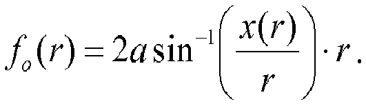
- The septums provided by embodiments of the present invention, as illustrated in
FIG. 5A , provide benefits not available using conventional polishing techniques. The shape of the septum is designed, using the Preston equation as described in relation toFIGS. 6 and 7 , to provide for a uniform pad wear rate as a function of position across the optic. In some embodiments, the uniformity of pad wear is characterized by a pad wear rate value differing less than 5% over the portion of the pad in contact with the optical element. In other embodiments, the pad wear rate value differs less than 2%, less than 1.5%, less than 1%, less than 0.75%, less than 0.5%, less than 0.4%, less than 0.3%, less than 0.3%, less than 0.2%, less than 0.1%, less than 0.05%, less than 0.025%, or less than 0.01%. For example, a first pad wear rate as a function of position is associated with the wear due to the optical element and a second pad wear rate as a function of position is associated with the septum (seeFIG. 6 ). The sum of these pad wear rates provides a substantially uniform rate at portions of the pad that are in contact with the optical element. Although some embodiments provides less than a wave of As will be evident to one of skill in the art, the pad wear rate uniformity extends to portions of the pad not in contact with the optical element (e.g., at radial distances less than 25 mm and greater than 125 mm inFIG. 6 ) as appropriate to the particular application, although the uniformity may decrease in these regions. One of ordinary skill in the art would recognize many variations, modifications, and alternatives. - It should be noted that the use of septums as described herein may also have other mutual benefits in addition to improving spatial pad wear uniformity, due to other phenomena that scale linearly with velocity and pressure. Some examples of such phenomena include pad compression and viscoelasticity, pad glazing, friction-induced temperature effects, slurry distribution, and the like.
- Utilizing embodiments of the present invention, the pad wear as a function of position is substantially uniform as a function of position, for example, less than several waves for optical elements. In an embodiment, the pad wear uniformity is within a wave over the radial distance in contact with the optical element, although the uniformity may be characterized by even more uniform pad wear, for example, less than a wave.
-
FIG. 7 is a simplified plot of septum width as a function of radial distance according to an embodiment of the present invention. The septum width inFIG. 7 (i.e., a circumferential width) is bounded by the maximum thickness set by the circumference of the lap at the particular radial distance (there is only so much circumference available to cover with the septum at small radial distances) and the minimum thickness set by the viscoelastic and the rigid punch effect. For softer pads, the viscoelastic effect is more prominent, whereas for harder pads, the rigid punch effect is more prominent. - In
FIG. 7 , the shape of the septum is determined for a circular optic, but other shapes for the optical element are included within the scope of the present invention. Utilizing the equations described herein, the loading of the septum can be different from the loading of the optic, for example, even a non-uniform loading. The function fo(s) can be calculated for a given shape, for example, a circular or rectangular optic, and then put into this formula to define the septum shape. The functions fo(r) and fs(r), called circumferential widths here, are defined as the fraction of the lap circumference at radius r that is covered by the optic or septum, respectively. - It will be appreciated that at portions of the septum near the center of the polisher (small radial distances on the lap), the constant value illustrated in
FIG. 6 may not be achievable since the radial velocity tends toward zero as the radial distance decreases. However, since the optic is located a finite distance from the center (e.g., 25 mm in the illustrated embodiment), this design constraint is met by the septum designs described herein. Because the optic does not overlap with radial distances less than 25 mm, a design flexibility for the constant pad wear rate is provided at radial distances not overlapping with the optic. -
FIGS. 8A-8C are simplified plots of septum load as a function of radial distance according to an embodiment of the present invention. Embodiments of the present invention can utilize septums that uniformly loaded (FIG. 8A ), differentially loaded (FIG. 8B ), or continuously loaded (FIG. 8C ). The plots inFIGS. 8A-8C illustrate that, as discussed in relation to the pad wear rate, the load (σ(r)) can be a function of position. -
FIG. 9A is a simplified schematic diagram illustrating scratching by rogue particles. In some optical element polishing applications, for example, for high energy laser and amplifier systems, stringent requirements can be placed on the scratch density. Without limiting embodiments of the present invention, the inventors believe that some scratches are caused during polishing by rogue particles, which are particles larger than other particles present in the polishing slurry, for example, either a foreign particle or particles with a particle size distribution larger than the average particle size of the other particles in the slurry. As shown inFIG. 9A , the rogue particles produce a higher load on the optic and produce a scratch or a series of scratches. Despite attempts to filter out rogue particles, scratching of optics is still observed.FIG. 9B is an image illustrating scratching by rogue particles. - Without limiting embodiments of the present invention, the inventors believe that an additional source producing rogue particles is the drying of the slurry. For example, for polishing compounds including cerium oxide, not only does the slurry dry out, but it chemically reacts with itself to produce, from a soft agglomerate, a hard agglomerate upon drying. The agglomerates can then produce scratches as illustrated in
FIG. 9B . - Embodiments of the present invention prevent drying of the slurry by enclosing the polishing system, which prevents foreign particles from entering, but also provides a high humidity environment so the slurry is prevented from drying out. A rinsing system can be used to rinse the optic when removed from the system to prevent slurry from remaining on the optic. Thus, the rinsed optic can be dried after removal without the drying of the slurry, which was removed during the rinsing process. As an additional aid in rinsing of slurry from the system, system components can be coated with a fluorinated polymer layer to reduce the adhesion between the slurry and the various system components.
-
FIG. 10 is a simplified perspective diagram of a high humidity polishing system according to an embodiment of the present invention. The highhumidity polishing system 1000 includes apolishing surface 1010, which can be a polishing pad, and an optic 1012 partially surrounded by aseptum 1014. Amoveable cover 1020 is able to be positioned in contact with anenclosure 1022 to form a controlled environment surrounding the polishing surface. Inputs and output ports for polishing slurry (not shown) and aninput port 1030 and anoutput port 1032 for a humid gas (e.g., water vapor) are provided as part of the system. - In the embodiment illustrated in
FIG. 10 , the humidity inside the polishing system is higher than the ambient humidity, for example, higher than 80%, higher than 85%, higher than 90%, higher than 95%, higher than 97%, higher than 98%, higher than 99% and up to 100%. In some embodiments, the humidity is provided at a high level to prevent substantial drying of the slurry in the system. The lack of drying in the environment prevents the formation of the hard agglomerates and the associated scratching. -
FIG. 11 is a simplified plan view of a portion of a high humidity polishing system differing in some respects from the high humidity polishing system illustrated inFIG. 10 . As illustrated inFIG. 11 , anoptic 1105 is placed on alap 1110 and spatially controlled using guide wheels. In the embodiment illustrated inFIG. 11 , a different septum design is used in which amirror septum 1120 is provided to produce uniform pad wear. A 100%humidity feed port 1030 is provided adjacent thelap 1110 so that the polishing environment can provide the desired controlled high humidity atmosphere in a manner similar to a sealed chamber (e.g., a hermetic chamber 1107). Embodiments of the present invention are not limited to the design illustrated inFIG. 11 , but this embodiment is provided merely by way of example. -
FIG. 12 illustrates plots of normalized interface height for polishing solutions at a range of dilutions as a function of time according to an embodiment of the present invention. The normalized interface height as a function of time provides insight into the settling properties of the illustrates slurries since the interface between the slurry and the solvent separating out of the slurry decreases in height as the slurry settles to the bottom of the container (e.g., a graduated cylinder). Hastilite PO mixed at a 1:4 ratio with DI water settles most quickly, with the normalized interface height dropping to 30% within about 25 minutes. A 1:1 dilution of Hastilite PO and DI water increases the settling time by an order of magnitude, with a 30% normalized interface height being reached in about 300 minutes. The undiluted Hastilite PO provides the longest settling time, dropping to around 60% at 300 minutes. Therefore, the dilution of the slurry, for example, Hastilite PO, impacts the settling time. -
FIG. 13 illustrates plots of normalized interface height for polishing solutions under the influence of agitation according to an embodiment of the present invention. As illustrated inFIG. 13 , agitation produces negligible differences in the settling times for the slurry diluted in either DI water or tap water. - In addition to dilution effects, the inventors have determined that stabilization of the slurry and increases in settling time can be achieved by the addition of an additive to the slurry that prevents agglomeration.
FIG. 14 illustrates plots of normalized interface height for polishing solutions as a function of time according to an embodiment of the present invention. The slurry illustrated inFIG. 14 is Hastilite PO, but other slurries are included within the scope of the present invention. Referring toFIG. 14 , Hastilite PO diluted to Baume 9 (squares) is characterized by the fastest settling time, dropping to 10% of the original normalized interface height in a period of about 30 minutes. The neat formulation of Hastilite PO (crosses) provides an increased settling time in a manner similar to the dilution effects illustrated inFIG. 12 . Addition of an additive to prevent agglomeration provides the greatest settling times as illustrated by Hastilite PO diluted toBaume 9 with 1% volume of the surfactant µ-90 (diamonds). As illustrated inFIG. 14 , the addition of the surfactant increases the settling time to provide a normalized interface height of almost 90% of the original height at 800 minutes. - Exemplary anionic surfactants in addition to µ-90 include Alkyl sulfates (e.g., Sodium dodecyl sulfate, ammonium lauryl sulfate, or the like); Alkyl sulfonates (e.g., Dodecyl benzene sulfonic acid,
Sulfonic 100, Calimulse EM-99, or the like); Alkyl ether phosphates (e.g., Triton H66, Triton QS44, or the like); Alkyl carboxylates (e.g. Sodium stearate or the like), or other suitable anionic surfactants. It should be noted that the surfactant, which can be used as an additive to the polishing slurry can include sodium, ammonium, or potassium salts in which the counterion is not active. The inventors have determined that the stabilization of the slurry by the surfactant (at an appropriate pH in some embodiments) provides for improved polishing results. - Embodiments of the present invention are not limited to the use of anionic surfactants, but can also use cationic surfactants. Exemplary cationic surfactants include Trimethylalkylammonium chlorides (e.g. cetyl trimethylammonium bromide (CTAB), distearyl dimethyl ammonium chloride, or the like); Benzalkonium chlorides; Alkylpyridinium chlorides (e.g. Cetyl pyridinium chloride); or other suitable cationic surfactants. It should be noted that the surfactant can include chloride or bromide salts in which the counterion is not active.
- In some implementations, the surfactant is effective to separate the polishing by-products from optical element undergoing polishing. The presence of the by-product can reduce the stability of the polishing slurry. In some embodiments, the surfactant is effective to prevent the agglomeration of the by-products, thereby increasing the long-term stability of the polishing slurry. Examples of by-products are cations (such as K+, Na+, Ca2+, Mg2+, etc) from the polished away glass during polishing.
- In some embodiments, the water used to prepare the slurry may contain varying concentrations of metallic cations. In addition, cations such as Na+, B3+, Fe2+, Ca2+, Mg2+, and Al3+ are released into the slurry as by-products of the polishing process. The presence of these ions has the potential to reduce stabilizer efficacy by disrupting the electrostatic interaction between the slurry particles and stabilizer molecules.
- Chelation agents (e.g., glycine, citric acid, ethylenediaminetetraacetic acid (EDTA), or the like) form favorable complexes with cations, sequestering them in solution and preventing their interaction with the slurry particles. Therefore, the addition of a chelation agent to the slurry may both improve initial stabilization efficiency and may prolong its stability as polishing by-products accumulate. Thus, embodiments of the present invention utilize chelation agents to improve slurry stabilization.
-
FIG. 15 is a simplified plot of relative interface height for stabilized and unstabilized polishing solutions as a function of time according to an embodiment of the present invention. As illustrated inFIG. 15 , the stabilization of the slurry by, for example, the addition of the anionic surfactant additive, produces significant increases in settling time. -
FIG. 16 is a polishing solution volume for stabilized and unstabilized polishing solutions as a function of particle size according to an embodiment of the present invention. In addition to increases in settling time and stabilization of the slurry, the addition of the additive to the slurry results in a reduction in the particle sizes in the slurry. Referring toFIG. 15 , the particle size distribution for the stabilized slurry is characterized by the majority of the particles being less than 1 µm in size, with a peak of the distribution at about 0.25 µm. For the unstabilized slurry, the peak of the distribution is centered at about 1 µm with either half or the majority of particles being characterized by the larger particle size distribution. The stabilized slurry results in an improved polishing outcome because the smaller particle size distribution provides smaller slurry particles during the polishing process. The inventors have demonstrated that the addition of the additive provides a slurry that is still characterized by an acceptable material removal rate and improved micro-roughness. - The inventors have determined that in some optical finishing operations utilizing grinding followed by polishing of thin optical elements, stress is introduced by the grinding operation, resulting in a tendency of the optical element to bend in response to the grinding induced stress. In order to reduce the stress, the optical element is chemically etched to remove surface layers, thereby reducing the stress present in the optical element. As an example, the optical element can be exposed to an acid or other suitable etchant (e.g., immersed in an acid bath) after grinding to remove a predetermined surface region of the optical element.
- In an embodiment, an optical element characterized by a first bend curvature is ground. After grinding, the optical element is characterized by a second bend curvature greater than the first bend curvature. In some embodiments, the increase in bend curvature results from stress introduced into the workpiece during the grinding process. The optical element is chemically etched to remove a predetermined portion of the optical element. After chemical etching, the optical element is characterized by a third bend curvature less than the second bend curvature. In some embodiments, the third bend curvature is less than or equal to the first bend curvature, returning the optical element to the curvature characterizing the optical element before the beginning of the finishing process. Thus, the chemical etching process reduces the stress introduced during grinding in some embodiments.
-
FIGS. 18A-18C are images illustrating surface curvature before grinding, after grinding, and after chemical etching according to an embodiment of the present invention. As illustrated inFIG. 18A , the surface curvature prior to grinding is characterized by a peak-to-valley value of 1.29 µm. Due to the instruction of stress by the grinding process, the surface curvature after grinding is characterized by a peak-to-valley value of 3.65 µm as illustrated inFIG. 18B . Embodiments of the present invention utilize chemical etching of the ground surface to remove residual stress present after the grinding process to return the figure to approximately the original shape as shown inFIG. 18C , in which the surface curvature after post-grinding etching is characterized by a peak-to-valley value of 1.16 µm. Thus, embodiments of the present invention provide methods and systems in which chemical etching is a useful mitigation technique to reduce or eliminate residual stress contributing to optic/lap mismatch. - The inventors have determined that in some polishing applications, pitch button bonding techniques can be used to improve the quality of the finished optical elements. Table 1 provides a summary of pitch button bonding (PBB) processes (also referred to as pitch button blocking processes) showing process parameters and the measured changes in surface figure, such as the change in the peak-to-valley height of the workpiece (also referred to as an optical element) (ΔPV), before and after blocking. As described herein, PBB includes a mounting technique that uses small islands of pitch between the workpiece and the mount that are cooled from the softening temperature of the pitch. At room temperature, the workpiece-pitch button-mount system is stiff, and the workpiece largely maintains its initial surface figure. After polishing using PBB techniques, the workpiece converges to the shape of the lap because, without limiting embodiments of the present invention, of the lack of workpiece bending and a dominance of the workpiece-lap mismatch due to the workpiece shape effect on the pressure distribution.
Table 1 Process Process Workpiece Pitch Process Temp (C) # of Buttons (N) Button Thick, t (mm) Button Diameter d (mm) Button spacing (dm) Area Fraction ΔPV (µm)* R16 S1 FS G73 65 37 1 10 4.6 0.370 -0.15 R13 S2 FS G73 65 37 1 10 4.6 0.370 -0.44 R14 S3 FS G82 72 3 1 10 41.2 0.030 -0.01 R15 S4 FS G82 72 4 1 9 35.3 0.032 0.00 R20 S5 FS G82 72 9 1.2 8 21.5 0.058 -0.06 R17 S6 FS G82 72 21 1.1 9 10.3 0.170 -0.08 R19 S7 FS G82 72 21 1.2 8 11.3 0.134 0.00 R7 S8 FS G82 72 37 1.1 11 3.6 0.448 -1.00 R8 S9 FS G82 72 37 0.9 12 2.6 0.533 -0.60 R9 S10 FS G82 72 37 0.8 13 1.6 0.625 -1.52 R10 S11 FS G82 72 37 1 11 3.6 0.448 -0.60 R11 S12 FS G82 72 37 0.7 14 0.6 0.725 -1.20 R12 S13 FS G82 72 37 0.8 11 3.6 0.448 -1.20 R31 S14 FS G82 78 1 2 NA NA 1.000 1.73 R107 S15 FS Cycad 75 37 1.2 8 6.6 0.237 -0.33 R104 S16 FS Cycad 75 37 1.3 7 7.6 0.181 -0.26 R3 S17 FS Cycad 92 1 NA NA NA 1.000 5.53 R73 S18 FS BP-1 60 11 0.85 5 21.7 0.028 0.00 R75 S19 FS BP-1 60 11 0.7 4.5 22.2 0.022 -0.10 R76 S20 FS BP-1 60 11 0.7 4.5 22.2 0.022 -0.02 R74 S21 FS BP-1 60 11 1.35 6.5 20.2 0.046 -0.04 R77 S22 FS BP-1 60 11 1.4 9 17.7 0.089 -0.03 R78 S23 FS BP-1 60 11 1.5 11.5 15.2 0.145 -0.18 R88 S24 FS BP-1 60 37 0.75 9 5.6 0.300 -0.15 R89 S25 FS BP-1 105 1 NA 0.5 NA 1.000 4.90 R91 S23 FS BP-1 105 1 NA 0.8 NA 1.000 6.40 R71 P1 P BP-1 60 11 0.6 4.5 22.2 0.022 0.04 R72 P2 P BP-1 60 11 0.9 4.5 22.2 0.022 0.03 R69 P3 P BP-1 60 11 0.8 6.5 20.2 0.046 0.23 R70 P4 P BP-1 60 21 0.6 5 14.3 0.053 0.43 R68 P5 P BP-1 60 11 1 7.5 19.2 0.062 0.28 R67 P6 P BP-1 63 11 0.6 9 17.7 0.089 0.46 R66 P7 P BP-1 70 11 0.4 13.5 13.2 0.200 1.10 R87 P8 P BP-1 60 37 0.55 8 6.6 0.237 1.10 R90 P9 P BP-1 105 1 NA 0.5 NA 1.000 7.90 R92 P10 P BP-1 105 1 NA 0.85 NA 1.000 9.90 P= Phosphate Glass; FS= fused silica; NA= not applicable; *sign convention (negative is convex, positive is concave) - The inventors have determined that an optical element (e.g., a fused silica or phosphate glass optic) can be bonded to a substrate (e.g., a stainless steel blank) using pitch buttons. The geometry of the pitch buttons, as described more fully below, prevents the deflection of the workpiece due to differences in coefficients of thermal expansion between the workpiece and the substrate. In some embodiments, isothermal cooling is utilized to reduce or eliminate deflection of the workpiece.
-
FIGS. 19A-19F are simplified schematic diagrams illustrating a method of performing pitch button bonding according to an embodiment of the present invention. As illustrated inFIG. 19A , an adhesion/protection layer that increases adhesion between the glass-pitch interface and protects the glass surface from staining due to the pitch contact, residual slurry making contact, and the like) is applied to surface S2 of the workpiece and the reflected wavefront is measured through surface S1. The adhesion/protection layer is a tape in some embodiments and the tape is optional in some embodiments. Pitch buttons are applied to the surface of the tape (or surface S2 of the workpiece) as illustrated inFIG. 19B . The application of the pitch buttons is performed in light of several variables including the pitch type, the radius (rp) of the pitch buttons, the thickness (tp) of the pitch buttons, the spacing (s) between pitch buttons, and the like. The pitch buttons are annealed (e.g., in an oven) using, for example, heating elements, as illustrated inFIG. 19C . The temperature of the annealing process, which may vary as a function of time, is selected to bring the whole system (e.g., glass, block, & pitch) to an elevated temperature near the temperature of the pitch at which the pitch starts to undergo significant stress relaxation (referred to as Tg) of the pitch and then cool the system as isothermally as possible to prevent or reduce the impact of residual stresses deforming the workpiece shape. -
FIG. 19D illustrates attachment of the workpiece with annealed pitch buttons to a preheated substrate (e.g., an aluminum or stainless steel block) with sufficient rigidity and mechanical properties for use during a polishing operation. Shims of a predetermined thickness (e.g., 1.25 mm) may be used during the mounting of the workpiece to the substrate. The mounted structure is then centered on the substrate, cooled, for example, using air cooling, and the shims are removed as illustrated inFIG. 19E . To characterize the optical properties of the workpiece after mounting, the reflected wavefront can be measured through surface S1 as illustrated inFIG. 19F . -
FIG. 20 is a plot illustrating the measured change in surface figure of fused silica and phosphate glass in various PPB configurations according to an embodiment of the present invention. As shown inFIG. 20 , the changes in surface figure of fused silica (FS) and phosphate glass (PG) optical elements for three conditions are shown. The workpieces used in the measurements shown inFIG. 20 were 100 mm in diameter with a thickness of 2.2 mm. For bonding with a solid layer of pitch, the relative surface height (FS) varies from about 7.5 µm at peripheral portions to about 3.7 µm at central portions and from about 10.1 µm to about 4.2 µm for PG. - Mounting of the workpiece using PBB techniques reduced the relative surface height variation considerably, using first, an un-optimized PBB technique that produced a variation of about half a micron of convex curvature (FS) and concave curvature (PS). By optimizing the PBB process as described herein, the variation in relative surface height is effectively reduced to zero as shown in
FIG. 20 . -
FIG. 21 is a plot of measured thermal expansion of pitches according to an embodiment of the present invention. Referring toFIG. 21 , the thermal expansion of two pitches, (Blocking Pitch-1 Black, available from Universal Photonics and Cycad Blackgold optical polishing pitch available from Cycad Products) as measured using a thermal-mechanical analysis, is illustrated. As the temperature increases, the pitches increase in dimension, with a measured coefficient of thermal expansion of 37 x 10-6 °C-1 for BP1 and 43 x 10-6 °C-1 for Cycad. -
FIG. 22A is a plot of workpiece peak-to-valley (PV) height as a function of undercooling of pitch for a single button and three buttons according to an embodiment of the present invention. InFIGS. 22A-22D , a fused silica workpiece (dw=100 mm diameter, tw=2.2 mm, Ep = 73 GPa, α = 5.4 x 10⁻⁷ °C-1) was utilized. The workpiece PV height after PPB is plotted as a function of degree of undercooling of the pitch for a single button (r = 25 mm) as well as for 3 buttons (s = 50 mm; r = 10 mm). The use of multiple pitch buttons significantly reduced the workpiece PV height. -
FIG. 22B is a plot of workpiece peak-to-valley height as a function of pitch button radius according to an embodiment of the present invention. The pitch button radius impacts the workpiece PV height as shown inFIG. 22B , which plots the PV height for a single button case and for various pitch moduli, thickness, and thermal expansion coefficients; (AT=54 °C). -
FIG. 22C is a plot of normalized workpiece peak-to-valley height as a function of pitch button offset according to an embodiment of the present invention. The PV height after PBB is normalized inFIG. 22C by dividing it by the relative total button area in microns and plotted as a function of the separation distance between buttons (dm), measured in millimeters for 3 button and 9 button cases. For the 3 button cases, the size of the pitch buttons are varied from 10 mm radius to 20 mm radius. The pitch button parameters were ΔT = 54 °C; t = 1 mm; Ep = 0.22 GPa; αp = 54 x 10-6 °C-1. The curve inFIG. 22C represents an empirical curve fit to the computed data. -
FIG. 22D is a plot ofworkpiece peak-to-valley height as a function of relative total pitch button area according to an embodiment of the present invention.FIG. 22D illustrates 3 and 9 button cases after PPB in which the spacing between buttons is kept at a value greater than 20 mm. The line inFIG. 22D represents an empirical curve fit to the computed data. -
FIG. 23 is a simplified schematic diagram illustrating pitch button bonding parameters according to an embodiment of the present invention. The PBB parameters include the modulus (Ep and Ew), coefficient of thermal expansion (αp and αw), and the thickness (tp and tw) of both the pitch buttons and the workpiece, respectively. The PBB parameters also include the radius of the pitch buttons (rp), the radius of the workpiece (rw), the center to center separation between pitch buttons (s), and the spacing between pitch buttons (dm). The total number of pitch buttons is indicated by N. The pitch buttons can have uniform dimensions or varying dimensions as appropriate to the particular application. Thus, both material and geometric parameters are utilized in the methods and systems described herein. -
FIGS. 24A and 24B are drawings illustrating optimized pitch button bonding patterns for optical elements according to an embodiment of the present invention. InFIG. 24A , an optimized PBB pattern is illustrated for a 100 mm diameter fused silica workpiece (i.e., Samples S18-S20). InFIG. 24B , an optimized PBB patter is illustrated for a 100 mm diameter phosphate glass workpiece (Samples P1-P2). -
FIG. 25A is a plot of workpiece peak-to-valley height as a function of spacing between buttons according to an embodiment of the present invention.FIG. 25A illustrates the change in surface figure of a fused silica workpiece (i.e., 100 mm diameter x 2.2 mm thick FS optical element) in various PPB configurations using pitch materials as a function of button spacing (dm).FIG. 25B is a plot of workpiece peak-to-valley height as a function of area fraction according to an embodiment of the present invention. The change in surface figure of both fused silica and phosphate glass workpieces (i.e., 100 mm diameter x 2.2 mm thick workpieces) is illustrated in various PBB configurations (N=11 and dm > 20 mm) as a function of area fraction. The points inFIG. 25B represent measured data and the lines are curve fits using αp = 2.4 x 10⁻⁶ °C-1. -
FIG. 26 is a simplified flowchart illustrating a method of determining pitch button bonding parameters according to an embodiment of the present invention. The method includes determining a peak-to-valley (PV) height value (2610) and determining a value related to pitch area (2612). In an embodiment, the PV height value can be a minimum acceptable PV height measured in terms of dimensions (e.g., 0.05 µm) or in terms of the wavelength of light transmitted by the optical element (e.g., λ/10). The value related to the pitch area (which can be referred to as an area constant) can be approximated by the PV height variation associated with a solid layer of pitch (e.g., C = 1.0 µm). The area constant C can be determined in some embodiments by measuring the PV height associated with a solid pitch layer and can be valid for a given material system based on the processing conditions (ΔT = 54 °C), the coefficient of thermal expansion (e.g., αp = 54 x 10-7 °C-1), modulus (e.g., Ep = 0.22 GPa), pitch thickness (tp = 1.0 mm), and the like. Typically, the values of the area constant will scale as:
- The method also includes computing a relative area of pitch (Ar) (2614), which is computed as:

- The method further includes computing a button radius (rp) (2616), which is computed using:

- The method additionally includes computing the number of pitch buttons (N) (2618), which may be evenly spaced. The N pitch buttons are then applied to the workpiece (2620) in accordance with the parameters computed using the method in order to couple the pitch buttons to the workpiece. As illustrated in
FIG. 19B , the pitch buttons can be applied to an adhesive and/or protective material such as a tape or other suitable material coupled to the workpiece. The workpiece is then mounted to a substrate, e.g., an optical flat comprising stainless steel, aluminum, combinations thereof, or the like, by coupling the N pitch buttons to the substrate (2622). - It should be appreciated that the specific steps illustrated in
FIG. 26 provide a particular method of determining pitch button bonding parameters according to an embodiment of the present invention. Other sequences of steps may also be performed according to alternative embodiments. For example, alternative embodiments of the present invention may perform the steps outlined above in a different order. Moreover, the individual steps illustrated inFIG. 26 may include multiple sub-steps that may be performed in various sequences as appropriate to the individual step. Furthermore, additional steps may be added or removed depending on the particular applications. One of ordinary skill in the art would recognize many variations, modifications, and alternatives. - To summarize, the subject matter described in the following sub-paragraphs, which are numbered to allow easy reference, is part of the disclosure of the present application, and can be claimed in the present application, and in one or more future divisional applications there from:
- (1) A polishing system for polishing an optical element, the polishing system comprising: a polishing pad having a radial dimension; and a septum disposed on the polishing pad and configured to partially surround the optical element, wherein the optical element contacts the polishing pad over a range of the radial dimension and a pad wear rate of the polishing pad is substantially constant as a function of radial dimension over the range of the radial dimension.
- (2) The polishing system of sub-paragraph (1) above, wherein the optical element comprises a circular lens.
- (3) The polishing system of sub-paragraph (1) above, wherein the septum comprises: a structural layer; a compliance layer; and a polishing layer.
- (4) The polishing system of sub-paragraph (3) above, wherein the structural layer is characterized by a higher density than the compliance layer or the polishing layer.
- (5) The polishing system of sub-paragraph (3) above, wherein the optical element comprises an optical material and the polishing layer comprises the optical material.
- (6) The polishing system of sub-paragraph (5) above, wherein the optical material comprises fused silica.
- (7) The polishing system of sub-paragraph (1) above, wherein the polishing pad is operable to receive a slurry comprising an abrasive components supported in a solvent and an additive.
- (8) The polishing system of sub-paragraph (7) above, wherein the additive comprises a surfactant.
- (9) The polishing system of sub-paragraph (8) above, wherein the surfactant comprises a anionic surfactant.
- (10) The polishing system of sub-paragraph (8) above, wherein the surfactant comprises a cationic surfactant.
- (11) The polishing system of sub-paragraph (1) above, further comprising a chamber surrounding the polishing pad and characterized by a humidity higher than an ambient humidity.
- (12) The polishing system of sub-paragraph (11) above, wherein the humidity is substantially 100%.
- (13) The polishing system of sub-paragraph (1) above, wherein the optical element is characterized by a peak-to-valley height that stabilizes at a fixed value after a predetermined polishing time.
- (14) A high humidity polishing system comprising: a polishing unit including a polishing pad; a slurry delivery system operable to provide a slurry to the polishing pad; and an enclosure surrounding the polishing unit, wherein a humidity inside the enclosure is sufficient to prevent substantial drying of the slurry.
- (15) The high humidity polishing system of sub-paragraph (14) above, wherein the humidity is characterized by a humidity higher than an ambient humidity.
- (16) The high humidity polishing system of sub-paragraph (15) above, wherein the humidity is substantially 100%.
- (17) The high humidity polishing system of sub-paragraph (14) above, wherein the slurry comprises a solvent, an abrasive component supported in the solvent, and an additive supported in the solvent.
- (18) The high humidity polishing system of sub-paragraph (14) above, wherein the polishing unit further includes a septum disposed adjacent the polishing pad and configured to partially surround an optical element contacting the polishing pad over a range of a radial dimension of the polishing pad and a pad wear rate of the polishing pad is substantially constant as a function of radial dimension over the range of the radial dimension.
- (19) The high humidity polishing system of sub-paragraph (18) above, wherein the slurry comprises a solvent, an abrasive component supported in the solvent, and a surfactant supported in the solvent.
- (20) A slurry system for polishing an optical element, the slurry system comprising: a solvent; an abrasive component supported in the solvent; and a surfactant supported in the solvent.
- (21) The slurry system of sub-paragraph (20) above, wherein the solvent comprises water.
- (22) The slurry system of sub-paragraph (20) above, wherein the abrasive component comprises at least one of cerium oxide or Hastilite PO.
- (23) The slurry system of sub-paragraph (20) above, wherein the surfactant comprises an anionic surfactant.
- (24) The slurry system of sub-paragraph (23) above, wherein the anionic surfactant comprises at least one of µ-90 or ammonium lauryl sulfate.
- (25) The slurry system of sub-paragraph (20) above, wherein the surfactant comprises a cationic surfactant.
- (26) The slurry system of sub-paragraph (20) above, further comprising a chelator.
- (27) A method of mounting a workpiece to a substrate, the method comprising: determining a peak-to-valley height value; determining a value related to pitch area; computing a relative area of pitch; computing a button radius; computing a number of pitch buttons; coupling N pitch buttons to the workpiece; and coupling the N pitch buttons to the substrate.
- (28) The method of sub-paragraph (27) above, wherein the peak-to-valley height value is based on a measurement of a peak-to-valley height associated with a solid pitch layer.
- (29) The method of sub-paragraph (27) above, wherein the relative area of pitch is equal to the peak-to-valley height value divided by the value related to pitch area.
- (30) The method of sub-paragraph (27) above, wherein a spacing between the N pitch buttons is substantially uniform.
- (31) The method of sub-paragraph (27) above, wherein coupling N pitch buttons to the workpiece comprises applying the N pitch buttons to a tape layer coupled to the workpiece.
- (32) The method of sub-paragraph (27) above, wherein the workpiece comprises an optical element and the substrate comprises an optical flat.
- It is also understood that the examples and embodiments described herein are for illustrative purposes only and that various modifications or changes in light thereof will be suggested to persons skilled in the art and are to be included within the spirit and purview of this application and scope of the appended claims.
Claims (15)
- A method of mounting a workpiece to a substrate, the method comprising:determining a peak-to-valley height value;determining a value related to pitch area;computing a relative area of pitch;computing a button radius;computing a number of pitch buttons;coupling the computed number, N, of pitch buttons to the workpiece; andcoupling the N pitch buttons to the substrate.
- The method of claim 1, wherein the peak-to-valley height value is based on a measurement of a peak-to-valley height associated with a solid pitch layer.
- The method of claim 1 or 2, wherein the relative area of pitch is equal to the peak-to-valley height value divided by the value related to pitch area.
- The method of claim 1, 2, or 3, wherein a spacing between the N pitch buttons is substantially uniform.
- The method of one of the preceding claims, wherein coupling the N pitch buttons to the workpiece comprises applying the N pitch buttons to a tape layer coupled to the workpiece.
- The method of one of the preceding claims, wherein the workpiece comprises an optical element and the substrate comprises an optical flat.
- A slurry system for polishing an optical element, in particular one which is mounted according to claim 6, the slurry system comprising:a solvent;an abrasive component supported in the solvent; anda surfactant supported in the solvent.
- The slurry system of claim 7, wherein the solvent comprises water.
- The slurry system of claim 7 or 8, wherein the abrasive component comprises cerium oxide.
- The slurry system of claim 7, 8, or 9, wherein the abrasive component comprises Hastilite PO.
- The slurry system of one of claims 7 to 10, wherein the surfactant comprises an anionic surfactant.
- The slurry system of claim 11, wherein the anionic surfactant comprises µ -90.
- The slurry system of claim 11 or 12, wherein the anionic surfactant comprises ammonium lauryl sulfate.
- The slurry system of one of claims 7 to 10, wherein the surfactant comprises a cationic surfactant.
- The slurry system of one of claims 7 to 15, comprising a chelator.
Applications Claiming Priority (3)
| Application Number | Priority Date | Filing Date | Title |
|---|---|---|---|
| US201161454893P | 2011-03-21 | 2011-03-21 | |
| PCT/US2012/029837 WO2012129244A1 (en) | 2011-03-21 | 2012-03-20 | Method and system for convergent polishing |
| EP12760262.1A EP2688712B1 (en) | 2011-03-21 | 2012-03-20 | Method and system for convergent polishing |
Related Parent Applications (1)
| Application Number | Title | Priority Date | Filing Date |
|---|---|---|---|
| EP12760262.1A Division EP2688712B1 (en) | 2011-03-21 | 2012-03-20 | Method and system for convergent polishing |
Publications (2)
| Publication Number | Publication Date |
|---|---|
| EP3187304A1 true EP3187304A1 (en) | 2017-07-05 |
| EP3187304B1 EP3187304B1 (en) | 2022-12-21 |
Family
ID=46879717
Family Applications (2)
| Application Number | Title | Priority Date | Filing Date |
|---|---|---|---|
| EP12760262.1A Active EP2688712B1 (en) | 2011-03-21 | 2012-03-20 | Method and system for convergent polishing |
| EP16207175.7A Active EP3187304B1 (en) | 2011-03-21 | 2012-03-20 | Method and system for convergent polishing |
Family Applications Before (1)
| Application Number | Title | Priority Date | Filing Date |
|---|---|---|---|
| EP12760262.1A Active EP2688712B1 (en) | 2011-03-21 | 2012-03-20 | Method and system for convergent polishing |
Country Status (6)
| Country | Link |
|---|---|
| EP (2) | EP2688712B1 (en) |
| JP (2) | JP5968418B2 (en) |
| KR (1) | KR20140019392A (en) |
| CN (1) | CN103534062A (en) |
| RU (1) | RU2610991C2 (en) |
| WO (1) | WO2012129244A1 (en) |
Cited By (1)
| Publication number | Priority date | Publication date | Assignee | Title |
|---|---|---|---|---|
| CN112405209A (en) * | 2020-11-11 | 2021-02-26 | 上饶市光耀光学设备制造有限公司 | Fine grinding and polishing device for processing optical lens |
Families Citing this family (2)
| Publication number | Priority date | Publication date | Assignee | Title |
|---|---|---|---|---|
| JP6321022B2 (en) * | 2012-11-02 | 2018-05-09 | ローレンス リバモア ナショナル セキュリティー, エルエルシー | Method for preventing aggregation of charged colloids without losing surface activity |
| CN110977679A (en) * | 2019-12-20 | 2020-04-10 | 成都精密光学工程研究中心 | Processing equipment and method for full-caliber low-defect planar workpiece |
Citations (4)
| Publication number | Priority date | Publication date | Assignee | Title |
|---|---|---|---|---|
| US6099604A (en) * | 1997-08-21 | 2000-08-08 | Micron Technology, Inc. | Slurry with chelating agent for chemical-mechanical polishing of a semiconductor wafer and methods related thereto |
| US6443811B1 (en) * | 2000-06-20 | 2002-09-03 | Infineon Technologies Ag | Ceria slurry solution for improved defect control of silicon dioxide chemical-mechanical polishing |
| US6692573B1 (en) * | 2000-06-01 | 2004-02-17 | Agilent Technologies, Inc. | Automated pitch button dispensing station and method |
| US20060234509A1 (en) * | 2005-04-15 | 2006-10-19 | Small Robert J | Cerium oxide abrasives for chemical mechanical polishing |
Family Cites Families (25)
| Publication number | Priority date | Publication date | Assignee | Title |
|---|---|---|---|---|
| JPH041532Y2 (en) * | 1985-03-19 | 1992-01-20 | ||
| JPS63283859A (en) * | 1987-05-13 | 1988-11-21 | Hitachi Ltd | Wafer polishing jig |
| JPH05228828A (en) * | 1992-02-19 | 1993-09-07 | Ibiden Co Ltd | Method and jig for polishing crystal body |
| JP3439501B2 (en) * | 1993-06-10 | 2003-08-25 | 株式会社住田光学ガラス | Lens joining device |
| CA2159797A1 (en) * | 1994-10-28 | 1996-04-29 | John H. Ko | Compliant lens block and tape |
| US5649849A (en) * | 1995-03-24 | 1997-07-22 | Eastman Kodak Company | Method and apparatus for realtime monitoring and feedback control of the shape of a continuous planetary polishing surface |
| JPH09117859A (en) * | 1995-10-27 | 1997-05-06 | Matsushita Electric Ind Co Ltd | Method of polishing substrate to be polished |
| JP3880102B2 (en) * | 1996-07-29 | 2007-02-14 | 東京エレクトロン株式会社 | Polishing apparatus and polishing method |
| US6149506A (en) * | 1998-10-07 | 2000-11-21 | Keltech Engineering | Lapping apparatus and method for high speed lapping with a rotatable abrasive platen |
| US7001252B2 (en) * | 2000-05-31 | 2006-02-21 | Jsr Corporation | Abrasive material |
| JP2003179021A (en) * | 2001-12-11 | 2003-06-27 | Sony Corp | Chemical mechanical polishing equipment |
| US6866559B2 (en) * | 2002-02-04 | 2005-03-15 | Kla-Tencor Technologies | Windows configurable to be coupled to a process tool or to be disposed within an opening in a polishing pad |
| US6866793B2 (en) * | 2002-09-26 | 2005-03-15 | University Of Florida Research Foundation, Inc. | High selectivity and high planarity dielectric polishing |
| JP2004330338A (en) * | 2003-05-06 | 2004-11-25 | Shin Etsu Chem Co Ltd | Work polishing apparatus and work polishing method |
| WO2006025641A1 (en) * | 2004-09-02 | 2006-03-09 | Joon-Mo Kang | Retaining ring for chemical mechanical polishing |
| US20060124592A1 (en) * | 2004-12-09 | 2006-06-15 | Miller Anne E | Chemical mechanical polish slurry |
| JP2006159384A (en) * | 2004-12-10 | 2006-06-22 | Tochigi Nikon Corp | Manufacturing method of optical components |
| JP4787063B2 (en) * | 2005-12-09 | 2011-10-05 | 株式会社荏原製作所 | Polishing apparatus and polishing method |
| JP2007298608A (en) * | 2006-04-28 | 2007-11-15 | Victor Co Of Japan Ltd | Method for manufacturing optical component |
| US7829464B2 (en) * | 2006-10-20 | 2010-11-09 | Spansion Llc | Planarization method using hybrid oxide and polysilicon CMP |
| WO2008058196A2 (en) * | 2006-11-08 | 2008-05-15 | St. Lawrence Nanotechnology, Inc. | Chemical mechanical polishing of moisture sensitive surfaces and compositions therefor |
| US20090284837A1 (en) * | 2008-05-13 | 2009-11-19 | Micron Technology, Inc. | Method and apparatus providing uniform separation of lens wafer and structure bonded thereto |
| US20090311945A1 (en) * | 2008-06-17 | 2009-12-17 | Roland Strasser | Planarization System |
| US8588956B2 (en) * | 2009-01-29 | 2013-11-19 | Tayyab Ishaq Suratwala | Apparatus and method for deterministic control of surface figure during full aperture polishing |
| JP5291746B2 (en) * | 2011-03-22 | 2013-09-18 | 株式会社荏原製作所 | Polishing equipment |
-
2012
- 2012-03-20 KR KR1020137027590A patent/KR20140019392A/en not_active Withdrawn
- 2012-03-20 RU RU2013146696A patent/RU2610991C2/en active
- 2012-03-20 EP EP12760262.1A patent/EP2688712B1/en active Active
- 2012-03-20 CN CN201280014310.8A patent/CN103534062A/en active Pending
- 2012-03-20 EP EP16207175.7A patent/EP3187304B1/en active Active
- 2012-03-20 JP JP2014501190A patent/JP5968418B2/en not_active Expired - Fee Related
- 2012-03-20 WO PCT/US2012/029837 patent/WO2012129244A1/en not_active Ceased
-
2016
- 2016-07-05 JP JP2016133727A patent/JP6232172B2/en active Active
Patent Citations (4)
| Publication number | Priority date | Publication date | Assignee | Title |
|---|---|---|---|---|
| US6099604A (en) * | 1997-08-21 | 2000-08-08 | Micron Technology, Inc. | Slurry with chelating agent for chemical-mechanical polishing of a semiconductor wafer and methods related thereto |
| US6692573B1 (en) * | 2000-06-01 | 2004-02-17 | Agilent Technologies, Inc. | Automated pitch button dispensing station and method |
| US6443811B1 (en) * | 2000-06-20 | 2002-09-03 | Infineon Technologies Ag | Ceria slurry solution for improved defect control of silicon dioxide chemical-mechanical polishing |
| US20060234509A1 (en) * | 2005-04-15 | 2006-10-19 | Small Robert J | Cerium oxide abrasives for chemical mechanical polishing |
Non-Patent Citations (1)
| Title |
|---|
| TAYYAB SURATWALA; RUSTY STEELE; MICHAEL FEIT; RICHARD DESJARDIN; DAN MASON: "Convergent Pad Polishing of Amorphous Silica", INTERNATIONAL JOURNAL OF APPLIED GLASS SCIENCE, SPECIAL ISSUE: PART 1, THE FLOW AND FRACTURE OF ADVANCED GLASSES, vol. 3, no. 1, March 2012 (2012-03-01), pages 14 - 28 |
Cited By (1)
| Publication number | Priority date | Publication date | Assignee | Title |
|---|---|---|---|---|
| CN112405209A (en) * | 2020-11-11 | 2021-02-26 | 上饶市光耀光学设备制造有限公司 | Fine grinding and polishing device for processing optical lens |
Also Published As
| Publication number | Publication date |
|---|---|
| JP5968418B2 (en) | 2016-08-10 |
| RU2013146696A (en) | 2015-04-27 |
| JP2016190318A (en) | 2016-11-10 |
| EP2688712B1 (en) | 2017-01-04 |
| CN103534062A (en) | 2014-01-22 |
| EP2688712A1 (en) | 2014-01-29 |
| JP2014511769A (en) | 2014-05-19 |
| EP2688712A4 (en) | 2015-07-15 |
| RU2610991C2 (en) | 2017-02-17 |
| EP3187304B1 (en) | 2022-12-21 |
| JP6232172B2 (en) | 2017-11-15 |
| WO2012129244A1 (en) | 2012-09-27 |
| KR20140019392A (en) | 2014-02-14 |
Similar Documents
| Publication | Publication Date | Title |
|---|---|---|
| JP5664471B2 (en) | Method for producing synthetic quartz glass substrate for semiconductor | |
| KR101704811B1 (en) | Method of processing synthetic quartz glass substrate for semiconductor | |
| KR101794488B1 (en) | Production method for composite substrate | |
| EP3548445A1 (en) | Strengthened glass-based articles and methods for reducing warp in strengthened glass-based articles | |
| TWI497196B (en) | Photomask-forming glass substrate and making method | |
| CN102794697B (en) | Method of manufacturing workpiece | |
| US20110189505A1 (en) | Method for manufacturing glass substrate for magnetic recording medium | |
| EP2688712B1 (en) | Method and system for convergent polishing | |
| KR20020027519A (en) | Process for reducing waviness in semiconductor wafers | |
| EP2236246B1 (en) | Method for producing large-size synthetic quartz glass substrate | |
| Arrasmith et al. | Use of magnetorheological finishing (MRF) to relieve residual stress and subsurface damage on lapped semiconductor silicon wafers | |
| CN116460667B (en) | Processing method of calcium fluoride optical part | |
| EP4123372A1 (en) | Mask blank substrate and method for manufacturing the same | |
| JP5473818B2 (en) | Polishing apparatus and polishing method | |
| JP2003186180A (en) | Pellicle frame manufacturing method and pellicle | |
| KR101912345B1 (en) | Apparatus for polishing surface of a curved cover glass | |
| JP7694474B2 (en) | Mask blank substrate and manufacturing method thereof | |
| Askinazi et al. | Development of large-aperture monolithic sapphire optical windows | |
| JP2010511203A (en) | Sub-aperture definitive ultra-precision finishing of high aspect ratio glass products | |
| KR102472858B1 (en) | Large-size synthetic quartz glass substrate, evaluation method, and manufacturing method | |
| EP4468078A2 (en) | Mask blank substrate and manufacturing method thereof | |
| KR100895780B1 (en) | Flat Panel Display Glass Substrates | |
| Lindquist et al. | Chemo-mechanical polishing of phosphate glass as a pretreatment to rapid final polishing | |
| Askinazi et al. | Recent advances in the application of computer-controlled optical finishing to produce very high-quality transmissive optical elements and windows |
Legal Events
| Date | Code | Title | Description |
|---|---|---|---|
| PUAI | Public reference made under article 153(3) epc to a published international application that has entered the european phase |
Free format text: ORIGINAL CODE: 0009012 |
|
| STAA | Information on the status of an ep patent application or granted ep patent |
Free format text: STATUS: REQUEST FOR EXAMINATION WAS MADE |
|
| 17P | Request for examination filed |
Effective date: 20161228 |
|
| AC | Divisional application: reference to earlier application |
Ref document number: 2688712 Country of ref document: EP Kind code of ref document: P |
|
| AK | Designated contracting states |
Kind code of ref document: A1 Designated state(s): AL AT BE BG CH CY CZ DE DK EE ES FI FR GB GR HR HU IE IS IT LI LT LU LV MC MK MT NL NO PL PT RO RS SE SI SK SM TR |
|
| STAA | Information on the status of an ep patent application or granted ep patent |
Free format text: STATUS: EXAMINATION IS IN PROGRESS |
|
| 17Q | First examination report despatched |
Effective date: 20180926 |
|
| REG | Reference to a national code |
Ref country code: DE Ref legal event code: R079 Ref document number: 602012079149 Country of ref document: DE Free format text: PREVIOUS MAIN CLASS: B24B0013005000 Ipc: B24B0037040000 |
|
| RIC1 | Information provided on ipc code assigned before grant |
Ipc: B24B 13/005 20060101ALI20210215BHEP Ipc: B24B 37/34 20120101ALI20210215BHEP Ipc: B24B 57/02 20060101ALI20210215BHEP Ipc: B24B 37/10 20120101ALI20210215BHEP Ipc: B24B 37/04 20120101AFI20210215BHEP |
|
| GRAP | Despatch of communication of intention to grant a patent |
Free format text: ORIGINAL CODE: EPIDOSNIGR1 |
|
| STAA | Information on the status of an ep patent application or granted ep patent |
Free format text: STATUS: GRANT OF PATENT IS INTENDED |
|
| INTG | Intention to grant announced |
Effective date: 20220715 |
|
| GRAS | Grant fee paid |
Free format text: ORIGINAL CODE: EPIDOSNIGR3 |
|
| GRAA | (expected) grant |
Free format text: ORIGINAL CODE: 0009210 |
|
| STAA | Information on the status of an ep patent application or granted ep patent |
Free format text: STATUS: THE PATENT HAS BEEN GRANTED |
|
| AC | Divisional application: reference to earlier application |
Ref document number: 2688712 Country of ref document: EP Kind code of ref document: P |
|
| AK | Designated contracting states |
Kind code of ref document: B1 Designated state(s): AL AT BE BG CH CY CZ DE DK EE ES FI FR GB GR HR HU IE IS IT LI LT LU LV MC MK MT NL NO PL PT RO RS SE SI SK SM TR |
|
| REG | Reference to a national code |
Ref country code: GB Ref legal event code: FG4D |
|
| REG | Reference to a national code |
Ref country code: DE Ref legal event code: R096 Ref document number: 602012079149 Country of ref document: DE |
|
| REG | Reference to a national code |
Ref country code: CH Ref legal event code: EP |
|
| REG | Reference to a national code |
Ref country code: AT Ref legal event code: REF Ref document number: 1538757 Country of ref document: AT Kind code of ref document: T Effective date: 20230115 |
|
| REG | Reference to a national code |
Ref country code: IE Ref legal event code: FG4D |
|
| REG | Reference to a national code |
Ref country code: LT Ref legal event code: MG9D |
|
| REG | Reference to a national code |
Ref country code: NL Ref legal event code: MP Effective date: 20221221 |
|
| PG25 | Lapsed in a contracting state [announced via postgrant information from national office to epo] |
Ref country code: SE Free format text: LAPSE BECAUSE OF FAILURE TO SUBMIT A TRANSLATION OF THE DESCRIPTION OR TO PAY THE FEE WITHIN THE PRESCRIBED TIME-LIMIT Effective date: 20221221 Ref country code: NO Free format text: LAPSE BECAUSE OF FAILURE TO SUBMIT A TRANSLATION OF THE DESCRIPTION OR TO PAY THE FEE WITHIN THE PRESCRIBED TIME-LIMIT Effective date: 20230321 Ref country code: LT Free format text: LAPSE BECAUSE OF FAILURE TO SUBMIT A TRANSLATION OF THE DESCRIPTION OR TO PAY THE FEE WITHIN THE PRESCRIBED TIME-LIMIT Effective date: 20221221 Ref country code: FI Free format text: LAPSE BECAUSE OF FAILURE TO SUBMIT A TRANSLATION OF THE DESCRIPTION OR TO PAY THE FEE WITHIN THE PRESCRIBED TIME-LIMIT Effective date: 20221221 |
|
| REG | Reference to a national code |
Ref country code: AT Ref legal event code: MK05 Ref document number: 1538757 Country of ref document: AT Kind code of ref document: T Effective date: 20221221 |
|
| PG25 | Lapsed in a contracting state [announced via postgrant information from national office to epo] |
Ref country code: RS Free format text: LAPSE BECAUSE OF FAILURE TO SUBMIT A TRANSLATION OF THE DESCRIPTION OR TO PAY THE FEE WITHIN THE PRESCRIBED TIME-LIMIT Effective date: 20221221 Ref country code: LV Free format text: LAPSE BECAUSE OF FAILURE TO SUBMIT A TRANSLATION OF THE DESCRIPTION OR TO PAY THE FEE WITHIN THE PRESCRIBED TIME-LIMIT Effective date: 20221221 Ref country code: HR Free format text: LAPSE BECAUSE OF FAILURE TO SUBMIT A TRANSLATION OF THE DESCRIPTION OR TO PAY THE FEE WITHIN THE PRESCRIBED TIME-LIMIT Effective date: 20221221 Ref country code: GR Free format text: LAPSE BECAUSE OF FAILURE TO SUBMIT A TRANSLATION OF THE DESCRIPTION OR TO PAY THE FEE WITHIN THE PRESCRIBED TIME-LIMIT Effective date: 20230322 |
|
| P01 | Opt-out of the competence of the unified patent court (upc) registered |
Effective date: 20230512 |
|
| PG25 | Lapsed in a contracting state [announced via postgrant information from national office to epo] |
Ref country code: NL Free format text: LAPSE BECAUSE OF FAILURE TO SUBMIT A TRANSLATION OF THE DESCRIPTION OR TO PAY THE FEE WITHIN THE PRESCRIBED TIME-LIMIT Effective date: 20221221 |
|
| PG25 | Lapsed in a contracting state [announced via postgrant information from national office to epo] |
Ref country code: SM Free format text: LAPSE BECAUSE OF FAILURE TO SUBMIT A TRANSLATION OF THE DESCRIPTION OR TO PAY THE FEE WITHIN THE PRESCRIBED TIME-LIMIT Effective date: 20221221 Ref country code: RO Free format text: LAPSE BECAUSE OF FAILURE TO SUBMIT A TRANSLATION OF THE DESCRIPTION OR TO PAY THE FEE WITHIN THE PRESCRIBED TIME-LIMIT Effective date: 20221221 Ref country code: PT Free format text: LAPSE BECAUSE OF FAILURE TO SUBMIT A TRANSLATION OF THE DESCRIPTION OR TO PAY THE FEE WITHIN THE PRESCRIBED TIME-LIMIT Effective date: 20230421 Ref country code: ES Free format text: LAPSE BECAUSE OF FAILURE TO SUBMIT A TRANSLATION OF THE DESCRIPTION OR TO PAY THE FEE WITHIN THE PRESCRIBED TIME-LIMIT Effective date: 20221221 Ref country code: EE Free format text: LAPSE BECAUSE OF FAILURE TO SUBMIT A TRANSLATION OF THE DESCRIPTION OR TO PAY THE FEE WITHIN THE PRESCRIBED TIME-LIMIT Effective date: 20221221 Ref country code: CZ Free format text: LAPSE BECAUSE OF FAILURE TO SUBMIT A TRANSLATION OF THE DESCRIPTION OR TO PAY THE FEE WITHIN THE PRESCRIBED TIME-LIMIT Effective date: 20221221 Ref country code: AT Free format text: LAPSE BECAUSE OF FAILURE TO SUBMIT A TRANSLATION OF THE DESCRIPTION OR TO PAY THE FEE WITHIN THE PRESCRIBED TIME-LIMIT Effective date: 20221221 |
|
| PG25 | Lapsed in a contracting state [announced via postgrant information from national office to epo] |
Ref country code: SK Free format text: LAPSE BECAUSE OF FAILURE TO SUBMIT A TRANSLATION OF THE DESCRIPTION OR TO PAY THE FEE WITHIN THE PRESCRIBED TIME-LIMIT Effective date: 20221221 Ref country code: PL Free format text: LAPSE BECAUSE OF FAILURE TO SUBMIT A TRANSLATION OF THE DESCRIPTION OR TO PAY THE FEE WITHIN THE PRESCRIBED TIME-LIMIT Effective date: 20221221 Ref country code: IS Free format text: LAPSE BECAUSE OF FAILURE TO SUBMIT A TRANSLATION OF THE DESCRIPTION OR TO PAY THE FEE WITHIN THE PRESCRIBED TIME-LIMIT Effective date: 20230421 Ref country code: AL Free format text: LAPSE BECAUSE OF FAILURE TO SUBMIT A TRANSLATION OF THE DESCRIPTION OR TO PAY THE FEE WITHIN THE PRESCRIBED TIME-LIMIT Effective date: 20221221 |
|
| REG | Reference to a national code |
Ref country code: DE Ref legal event code: R097 Ref document number: 602012079149 Country of ref document: DE |
|
| PLBE | No opposition filed within time limit |
Free format text: ORIGINAL CODE: 0009261 |
|
| STAA | Information on the status of an ep patent application or granted ep patent |
Free format text: STATUS: NO OPPOSITION FILED WITHIN TIME LIMIT |
|
| PG25 | Lapsed in a contracting state [announced via postgrant information from national office to epo] |
Ref country code: MC Free format text: LAPSE BECAUSE OF FAILURE TO SUBMIT A TRANSLATION OF THE DESCRIPTION OR TO PAY THE FEE WITHIN THE PRESCRIBED TIME-LIMIT Effective date: 20221221 Ref country code: DK Free format text: LAPSE BECAUSE OF FAILURE TO SUBMIT A TRANSLATION OF THE DESCRIPTION OR TO PAY THE FEE WITHIN THE PRESCRIBED TIME-LIMIT Effective date: 20221221 |
|
| REG | Reference to a national code |
Ref country code: CH Ref legal event code: PL |
|
| 26N | No opposition filed |
Effective date: 20230922 |
|
| REG | Reference to a national code |
Ref country code: BE Ref legal event code: MM Effective date: 20230331 |
|
| PG25 | Lapsed in a contracting state [announced via postgrant information from national office to epo] |
Ref country code: LU Free format text: LAPSE BECAUSE OF NON-PAYMENT OF DUE FEES Effective date: 20230320 |
|
| REG | Reference to a national code |
Ref country code: IE Ref legal event code: MM4A |
|
| PG25 | Lapsed in a contracting state [announced via postgrant information from national office to epo] |
Ref country code: SI Free format text: LAPSE BECAUSE OF FAILURE TO SUBMIT A TRANSLATION OF THE DESCRIPTION OR TO PAY THE FEE WITHIN THE PRESCRIBED TIME-LIMIT Effective date: 20221221 Ref country code: LI Free format text: LAPSE BECAUSE OF NON-PAYMENT OF DUE FEES Effective date: 20230331 Ref country code: IE Free format text: LAPSE BECAUSE OF NON-PAYMENT OF DUE FEES Effective date: 20230320 Ref country code: CH Free format text: LAPSE BECAUSE OF NON-PAYMENT OF DUE FEES Effective date: 20230331 |
|
| PG25 | Lapsed in a contracting state [announced via postgrant information from national office to epo] |
Ref country code: BE Free format text: LAPSE BECAUSE OF NON-PAYMENT OF DUE FEES Effective date: 20230331 |
|
| PG25 | Lapsed in a contracting state [announced via postgrant information from national office to epo] |
Ref country code: IT Free format text: LAPSE BECAUSE OF FAILURE TO SUBMIT A TRANSLATION OF THE DESCRIPTION OR TO PAY THE FEE WITHIN THE PRESCRIBED TIME-LIMIT Effective date: 20221221 |
|
| PG25 | Lapsed in a contracting state [announced via postgrant information from national office to epo] |
Ref country code: BG Free format text: LAPSE BECAUSE OF FAILURE TO SUBMIT A TRANSLATION OF THE DESCRIPTION OR TO PAY THE FEE WITHIN THE PRESCRIBED TIME-LIMIT Effective date: 20221221 |
|
| PG25 | Lapsed in a contracting state [announced via postgrant information from national office to epo] |
Ref country code: BG Free format text: LAPSE BECAUSE OF FAILURE TO SUBMIT A TRANSLATION OF THE DESCRIPTION OR TO PAY THE FEE WITHIN THE PRESCRIBED TIME-LIMIT Effective date: 20221221 |
|
| PG25 | Lapsed in a contracting state [announced via postgrant information from national office to epo] |
Ref country code: CY Free format text: LAPSE BECAUSE OF FAILURE TO SUBMIT A TRANSLATION OF THE DESCRIPTION OR TO PAY THE FEE WITHIN THE PRESCRIBED TIME-LIMIT; INVALID AB INITIO Effective date: 20120320 |
|
| PG25 | Lapsed in a contracting state [announced via postgrant information from national office to epo] |
Ref country code: HU Free format text: LAPSE BECAUSE OF FAILURE TO SUBMIT A TRANSLATION OF THE DESCRIPTION OR TO PAY THE FEE WITHIN THE PRESCRIBED TIME-LIMIT; INVALID AB INITIO Effective date: 20120320 |
|
| PG25 | Lapsed in a contracting state [announced via postgrant information from national office to epo] |
Ref country code: TR Free format text: LAPSE BECAUSE OF FAILURE TO SUBMIT A TRANSLATION OF THE DESCRIPTION OR TO PAY THE FEE WITHIN THE PRESCRIBED TIME-LIMIT Effective date: 20221221 |
|
| PGFP | Annual fee paid to national office [announced via postgrant information from national office to epo] |
Ref country code: GB Payment date: 20260327 Year of fee payment: 15 |
|
| PGFP | Annual fee paid to national office [announced via postgrant information from national office to epo] |
Ref country code: DE Payment date: 20260327 Year of fee payment: 15 |
|
| PGFP | Annual fee paid to national office [announced via postgrant information from national office to epo] |
Ref country code: FR Payment date: 20260325 Year of fee payment: 15 |