EP3185291A1 - A leadframe and a method of manufacturing a leadframe - Google Patents
A leadframe and a method of manufacturing a leadframe Download PDFInfo
- Publication number
- EP3185291A1 EP3185291A1 EP15201716.6A EP15201716A EP3185291A1 EP 3185291 A1 EP3185291 A1 EP 3185291A1 EP 15201716 A EP15201716 A EP 15201716A EP 3185291 A1 EP3185291 A1 EP 3185291A1
- Authority
- EP
- European Patent Office
- Prior art keywords
- leadframe
- copper
- alloy
- plating
- inlay
- Prior art date
- Legal status (The legal status is an assumption and is not a legal conclusion. Google has not performed a legal analysis and makes no representation as to the accuracy of the status listed.)
- Granted
Links
Images

Classifications
-
- H—ELECTRICITY
- H10—SEMICONDUCTOR DEVICES; ELECTRIC SOLID-STATE DEVICES NOT OTHERWISE PROVIDED FOR
- H10W—GENERIC PACKAGES, INTERCONNECTIONS, CONNECTORS OR OTHER CONSTRUCTIONAL DETAILS OF DEVICES COVERED BY CLASS H10
- H10W70/00—Package substrates; Interposers; Redistribution layers [RDL]
- H10W70/40—Leadframes
-
- H—ELECTRICITY
- H10—SEMICONDUCTOR DEVICES; ELECTRIC SOLID-STATE DEVICES NOT OTHERWISE PROVIDED FOR
- H10W—GENERIC PACKAGES, INTERCONNECTIONS, CONNECTORS OR OTHER CONSTRUCTIONAL DETAILS OF DEVICES COVERED BY CLASS H10
- H10W70/00—Package substrates; Interposers; Redistribution layers [RDL]
- H10W70/40—Leadframes
- H10W70/456—Materials
-
- H—ELECTRICITY
- H10—SEMICONDUCTOR DEVICES; ELECTRIC SOLID-STATE DEVICES NOT OTHERWISE PROVIDED FOR
- H10W—GENERIC PACKAGES, INTERCONNECTIONS, CONNECTORS OR OTHER CONSTRUCTIONAL DETAILS OF DEVICES COVERED BY CLASS H10
- H10W70/00—Package substrates; Interposers; Redistribution layers [RDL]
- H10W70/01—Manufacture or treatment
- H10W70/04—Manufacture or treatment of leadframes
-
- H—ELECTRICITY
- H10—SEMICONDUCTOR DEVICES; ELECTRIC SOLID-STATE DEVICES NOT OTHERWISE PROVIDED FOR
- H10W—GENERIC PACKAGES, INTERCONNECTIONS, CONNECTORS OR OTHER CONSTRUCTIONAL DETAILS OF DEVICES COVERED BY CLASS H10
- H10W70/00—Package substrates; Interposers; Redistribution layers [RDL]
- H10W70/40—Leadframes
- H10W70/451—Multilayered leadframes
-
- H—ELECTRICITY
- H10—SEMICONDUCTOR DEVICES; ELECTRIC SOLID-STATE DEVICES NOT OTHERWISE PROVIDED FOR
- H10W—GENERIC PACKAGES, INTERCONNECTIONS, CONNECTORS OR OTHER CONSTRUCTIONAL DETAILS OF DEVICES COVERED BY CLASS H10
- H10W70/00—Package substrates; Interposers; Redistribution layers [RDL]
- H10W70/40—Leadframes
- H10W70/456—Materials
- H10W70/457—Materials of metallic layers on leadframes
-
- H—ELECTRICITY
- H10—SEMICONDUCTOR DEVICES; ELECTRIC SOLID-STATE DEVICES NOT OTHERWISE PROVIDED FOR
- H10W—GENERIC PACKAGES, INTERCONNECTIONS, CONNECTORS OR OTHER CONSTRUCTIONAL DETAILS OF DEVICES COVERED BY CLASS H10
- H10W72/00—Interconnections or connectors in packages
- H10W72/50—Bond wires
- H10W72/531—Shapes of wire connectors
- H10W72/536—Shapes of wire connectors the connected ends being ball-shaped
-
- H—ELECTRICITY
- H10—SEMICONDUCTOR DEVICES; ELECTRIC SOLID-STATE DEVICES NOT OTHERWISE PROVIDED FOR
- H10W—GENERIC PACKAGES, INTERCONNECTIONS, CONNECTORS OR OTHER CONSTRUCTIONAL DETAILS OF DEVICES COVERED BY CLASS H10
- H10W72/00—Interconnections or connectors in packages
- H10W72/50—Bond wires
- H10W72/531—Shapes of wire connectors
- H10W72/5363—Shapes of wire connectors the connected ends being wedge-shaped
-
- H—ELECTRICITY
- H10—SEMICONDUCTOR DEVICES; ELECTRIC SOLID-STATE DEVICES NOT OTHERWISE PROVIDED FOR
- H10W—GENERIC PACKAGES, INTERCONNECTIONS, CONNECTORS OR OTHER CONSTRUCTIONAL DETAILS OF DEVICES COVERED BY CLASS H10
- H10W72/00—Interconnections or connectors in packages
- H10W72/851—Dispositions of multiple connectors or interconnections
- H10W72/874—On different surfaces
- H10W72/884—Die-attach connectors and bond wires
-
- H—ELECTRICITY
- H10—SEMICONDUCTOR DEVICES; ELECTRIC SOLID-STATE DEVICES NOT OTHERWISE PROVIDED FOR
- H10W—GENERIC PACKAGES, INTERCONNECTIONS, CONNECTORS OR OTHER CONSTRUCTIONAL DETAILS OF DEVICES COVERED BY CLASS H10
- H10W74/00—Encapsulations, e.g. protective coatings
-
- H—ELECTRICITY
- H10—SEMICONDUCTOR DEVICES; ELECTRIC SOLID-STATE DEVICES NOT OTHERWISE PROVIDED FOR
- H10W—GENERIC PACKAGES, INTERCONNECTIONS, CONNECTORS OR OTHER CONSTRUCTIONAL DETAILS OF DEVICES COVERED BY CLASS H10
- H10W90/00—Package configurations
- H10W90/701—Package configurations characterised by the relative positions of pads or connectors relative to package parts
- H10W90/751—Package configurations characterised by the relative positions of pads or connectors relative to package parts of bond wires
- H10W90/756—Package configurations characterised by the relative positions of pads or connectors relative to package parts of bond wires between a chip and a stacked lead frame, conducting package substrate or heat sink
Definitions
- the present disclosure relates to leadframes for integrated circuits, and methods of manufacturing leadframes.
- a method of manufacturing a leadframe comprising:
- Such a method can be economical and efficient.
- the first material comprises Alloy 42, and the second material comprises copper.
- the second material has a thickness of about 4 ⁇ m to 20 ⁇ m.
- the first material comprises copper
- the second material comprises Alloy 42.
- the copper comprises a copper alloy.
- the method further comprises: plating the leadframe with copper-plating.
- the copper-plating may have a thickness of less than about 2 ⁇ m.
- Plating the leadframe with copper-plating may comprise providing copper plating over a subset of the external surfaces of the leadframe.
- the indentation in the base layer comprises a groove.
- the groove may be substantially straight.
- the method may further comprise: engraving the groove in the second material.
- the method further comprises: applying pressure to the leadframe-material before forming the leadframe from the leadframe-material. This may involve applying pressure to the entire leadframe-material.
- leadframe comprising:
- the inlay is located at a bond pad region of the leadframe.
- leadframes are metal structures that are inside an integrated circuit package (chip) and carry signals from the die to a package lead, for connecting to the outside world. Bond wires can be used to electrically connect the die to the leadframe.
- the leadframe can include an Alloy 42 base material.
- Alloy 42 is a known material that comprises 42% nickel content and 58% iron content, and has a low coefficient of thermal expansion (CTE).
- CTE coefficient of thermal expansion
- the CTE of the leadframe can advantageously be matched with that of the die material. Therefore, when high temperatures are applied for the eutectic die bonding process, the die and the leadframe expand at similar rates and therefore reduce the likelihood of any mechanical difficulties when the materials subsequently cool down or heat up. For example, mechanical stress between the die and the leadframe as they contract.
- a copper layer can be located between the die and the Alloy 42.
- the copper layer should be thick enough to provide good thermal and electrical conductivity performance.
- the copper layer can be fabricated by a plating process, as discussed below with reference to figure 1 .
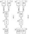
- Figure 1 shows schematically a process flow for manufacturing a leadframe.
- an Alloy 42 base raw material is received, which may be provided as a sheet from a roll. As indicated above, use of Alloy 42 can provide good CTE matching with the die.
- the Alloy 42 material is stamped into the desired shape of the leadframe.
- the stamped Alloy 42 material is plated with copper over its entire outer surface.
- the copper plate may be about 6 ⁇ m thick in order to provide good thermal and electrical conductivity performance.
- performing a plating operation for such a thick layer of copper may be disadvantageous in some examples. For example, it may be uneconomical or inefficient.
- Step 108 in figure 1 illustrates that an optional silver plating operation can be performed on the leadframe.
- Such silver plating can enhance the quality of bonding for subsequent connections to the die.
- a silver plating operation may not be used.
- a copper wire can be bonded directly onto a copper surface of the leadframe.
- One or more example embodiments disclosed herein can use a metal cladding technique to create a thick copper layer only at required locations in the raw material, instead of a plating process such as the one illustrated in figure 1 .
- Figure 2 shows schematically an example embodiment of a process flow for manufacturing a leadframe.
- the method receives an Alloy 42 base raw material, which again may be provided as a sheet from a roll.
- the Alloy 42 base material includes an indentation, which can be provided as a groove running continuously along the sheet.
- a copper inlay is inserted into indentation in the Alloy 42 material.
- This provides a leadframe-material that comprises both a base layer that comprises a first material (Alloy 42 in this example) and an inlay that comprises a second material (copper in this example).
- the copper inlay may have a thickness of about 4 ⁇ m to 20 ⁇ m, or about 4 ⁇ m to 10 ⁇ m, or about 5 ⁇ m to 7 ⁇ m. It will be appreciated that the specific thickness of the copper inlay may depend upon a specific application, and that the copper inlay should be thick enough to provide the leadframe with desired electrical and thermal properties.
- a material that comprises copper includes copper alloys, and derivatives of copper. Therefore any reference to copper in this document should be construed as covering copper alloys and copper derivatives.
- the indentation in the Alloy 42 base raw material can be provided only at locations in the eventual leadframe that require the improved electrical and thermal conductivity that is provided by the copper.
- Such locations can include the position of bond pads in the final leadframe, such as pads for die bonding and wire bonding. Therefore, regions of the leadframe that do not require improved electrical and thermal productivity do not necessarily include a region of copper inlay.
- the insertion of the inlay may be referred to as a metal cladding operation.
- a leadframe is formed from the leadframe-material.
- the leadframe is formed by stamping the leadframe-material into the desired shape of the leadframe. Such stamping can remove material that is not required for the leadframe.
- a leadframe can be provided that has an appropriate amount / thickness of copper in regions that require electrical and thermal conductivity, whilst retaining a sufficient amount of Alloy 42 such that the leadframe as a whole has the necessary CTE properties.
- the leadframe can be formed out of the leadframe-material by an etching operation.
- use of such an inlay can be convenient for using copper alloys with different properties for the inlay, for different thermal and electrical conductivity applications.
- the leadframe can also be applied to approaches in which copper wires applied to bare copper bond pads.
- the leadframe may also not require additional silver plating.
- eliminating a thick copper plating process can widen the leadframe supply.
- use of an inlay can provide an efficient and economical method of manufacturing a leadframe with desired electrical, thermal and CTE properties.
- the method of figure 2 can apply a metal cladding technique to create a thick copper layer at the required location in the raw material. Upfront design of the raw material may be involved to provide the necessary indentations. The metal cladded raw material can then be used in subsequent leadframe manufacture.
- the method involves the optional step of performing a copper flash plating operation.
- a plating operation can involve plating the leadframe with a relatively thin copper layer, for example one that is about 1 ⁇ m thick.
- the relatively thin copper layer may have a thickness of less than about than 2 ⁇ m or 1 ⁇ m.
- the thin copper layer can provide a smooth and consistent finish to the leadframe.
- Plating a thin copper layer in optional step 208 of figure 2 may not suffer from the same inefficiencies as occur when plating a thick copper layer, as discussed above with reference to figure 1 .
- the method of figure 2 can include an optional silver plating operation 210, or the silver plating operation can be skipped (step 212).
- a leadframe manufactured according to the method of figure 2 can be used in plastic surface-mounted packages, such as SOT23 from NXPTM.
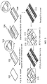
- Figure 3 shows graphically the steps involved in an example embodiment of manufacturing a leadframe.
- Figure 3 shows a base layer 302 of Alloy 42 raw material.
- a mechanical process is used in this example to engrave slots / grooves 304 at locations that will correspond to bond pad positions in the final leadframe.
- the grooves 304 in this example are substantially straight, which can be convenient for manufacture.
- copper strips / inlays 306 are inserted into the grooves 304 and are clad directly to the Alloy 42 material.
- the cladding operation may involve applying pressure to the interface between the base layer 302 and the inlays 306 such that the two different materials then are provided together as a single sheet of leadframe-material 308.
- a carving tool can be installed in a rolling passage of the base layer 302 such that the groove 304 is carved out as the base layer 302 is rolled reel-to-reel.
- a rolling tool can be used to form and shape the groove.
- the inlays 306 can be applied in-line in the rolling passage, to complete the cladded insert in the reel-to-reel leadframe.
- the cladding process can be considerably less expensive than the plating process of figure 1 , and can make more efficient use of materials.
- the base layer may be provided pre-processed with the indentations / groves 304 and therefore an engraving operation may not be required.
- each leadframe-material 308 is then stamped or etched in order to provide a sheet of material that includes a plurality of individual leadframes.
- each leadframe includes three bond pad regions 310, 312, 314 because the corresponding chip will have three leads. It can be seen from figure 3 that each bond pad region 310, 312, 314 corresponds to a location in the leadframe that includes a copper inlay.
- the leadframe is subsequently plated with a layer of copper that is relatively thin. For example, less than 2 ⁇ m, 1 ⁇ m or 0.5 ⁇ m.
- a close up view of a single copper plated leadframe 316 (for a single IC) is shown in figure 3 .
- Figure 4 shows an example embodiment of an integrated circuit (IC) 400 that includes a leadframe 402 that has been manufactured according to figure 3 .
- the IC 400 has three leads / pins, although only a first lead 408a and a second lead 408b can be seen in figure 4 .
- the leadframe 400 includes three components 402a, 402b, 402c, one for each lead, which are shown as separate from each other in figure 4 because the outside of the leadframe shown in figure 3 has been removed.
- a die 404 is shown as attached to a second component 402b of the leadframe.
- the die 404 is attached to a first component 402a of the leadframe by a first bond wire 406a.
- the die 404 is attached to a third component 402c of the leadframe by a third bond wire 406c.
- the die 404 and the bond wires 406a, 406c are attached to each the components 402a, 402b, 402c of the leadframe at bond pad regions of the leadframe. As discussed above with reference to figure 3 , each of these bond pad regions corresponds to a location of the leadframe that has the copper inlay (not visible in figure 4 ).
- the leads of the IC 400 that are outside a plastic casing 410 of the device, are regions of the leadframe 402 that have been plated with tin.
- Figure 5a shows a side view of the IC 400 of figure 4 . Feature of figure 5a that have already been described with reference to figure 4 have been given corresponding reference numbers in the 500 series, and will not necessarily be described again here. In figure 5a , the second lead / pin 508c is also visible.
- Figure 5b shows a close up view of the end of one of the leads of the IC of figures 4 and 5a .
- the view of figure 5b shows the three separate materials that make up this part of the leadframe.
- An outer layer of tin plating 512 is shown.
- a thin layer of copper plating 514 Immediately inside the layer of tin plating 512 is a thin layer of copper plating 514.
- this layer of copper plating 514 may have a thickness of about 1 ⁇ m, and is not included to significantly improve the electrical and thermal conductivity of the leadframe in the bond pad regions.
- the Alloy 42 base layer 516 Inside the thin layer of copper plating 514.
- Figure 6a shows a side view of an IC 600 that has been manufactured according to the method of figure 1 ; that is, one in which a thick layer of copper plating has been used to provide the requisite electrical and thermal conductivity.
- the features of figure 6a will not be described in detail because, externally at least, figure 6a is very similar to figure 5a .
- Figure 6b shows a close up view of the end of one of the leads of the IC 600 of figure 6a .
- the view of figure 6b shows the materials that make up this part of the leadframe, which are the same materials as shown in figure 5b .
- the layer of copper plating 614 is much thicker. This is because this layer of copper plating 614 is also included in the bond pad regions to provide the requisite electrical and thermal conductivity of the leadframe.
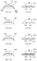
- Figures 7, 8, 9 and 10 illustrate cross-sectional end views of four different ICs. In these views, various dimensions of layers of material have been exaggerated for ease of illustration.
- Figure 7a shows a cross-sectional end view of an IC 700, and shows a die 704, a first and third lead 708a, 708c that are one behind the other, and a second lead 708b.
- the leads 708a, 708b, 708c, which are external to the plastic casing 740 of the IC 700, are plated with tin.
- Figure 7b shows a close up view of the die 704 and a bond pad region 702 of the leadframe.
- the leadframe of the IC of figures 7a and 7b has been manufactured using a full copper plating operation on the entire leadframe, with a copper thickness of about 6 ⁇ m. Therefore, the thickness of the copper plating 714 is consistent around the entire leadframe (both at the bond pad region 702, and at regions outside the bond pad region 702).
- Figure 8a shows a cross-sectional end view of another IC 800, and shows a die 804.
- Figure 8b shows a close up view of the die 804 and a bond pad region 802 of the leadframe.
- the leadframe of the IC has been manufactured using a copper inlay / insert at only the bond pad regions, and copper plating operation has been used. Therefore, the only copper material 814 that is present in the leadframe at the bond pad region 802, which in this example is on a top side of a pad / lead area.
- Figure 9a shows a cross-sectional end view of another IC 900, and shows a die 904.
- Figure 9b shows a close up view of the die 904 and a bond pad region 902 of the leadframe.
- the leadframe of the IC has been manufactured using a copper inlay at the bond pad regions, and also a flash copper plating operation. Therefore, the IC includes an inlay-portion 914 of copper material that is present in the leadframe at the bond pad region 802, as provided by the inlay.
- the IC also includes an outer-portion 915 of copper material over the entire leadframe, with a copper thickness of about 1 ⁇ m, as provided by the flash copper plating operation. It will be appreciated that in other examples, outer-portion 915 of copper material need not necessarily be provided over the entire leadframe; it could be provided over a subset of the external surfaces of the leadframe.
- Figure 10a shows a cross-sectional end view of another IC 1000, and shows a die 1004.
- the base layer of the leadframe comprises a copper alloy
- the inlay comprises Alloy 42. That is, the materials for the base layer and the inlay of figure 9a have generally been reversed.
- Figure 10b shows a close up view of the die 1004 and a bond pad region 1002 of the leadframe.
- the leadframe of the IC has been manufactured using an Alloy 42 inlay at the bond pad regions, and also a flash copper plating operation. Therefore, the IC includes an inlay-portion 1014 of Alloy 42 material that is present in the leadframe at the bond pad region 1002, as provided by the inlay.
- the IC also includes an outer-portion 1015 of copper material over the entire leadframe.
- One or more of the examples disclosed herein include a relatively thick copper layer created on a top area of a leadframe for bonding, instead of uniformly covering all of the leadframe surface with a thick copper layer.
- the leadframe can include a clad metal insert on the functional area and may not require a clad metal sheet on the whole leadframe.
- the set of instructions/method steps described above are implemented as functional and software instructions embodied as a set of executable instructions which are effected on a computer or machine which is programmed with and controlled by said executable instructions. Such instructions are loaded for execution on a processor (such as one or more CPUs).
- processor includes microprocessors, microcontrollers, processor modules or subsystems (including one or more microprocessors or microcontrollers), or other control or computing devices.
- a processor can refer to a single component or to plural components.
- the set of instructions/methods illustrated herein and data and instructions associated therewith are stored in respective storage devices, which are implemented as one or more non-transient machine or computer-readable or computer-usable storage media or mediums.
- Such computer-readable or computer usable storage medium or media is (are) considered to be part of an article (or article of manufacture).
- An article or article of manufacture can refer to any manufactured single component or multiple components.
- the non-transient machine or computer usable media or mediums as defined herein excludes signals, but such media or mediums may be capable of receiving and processing information from signals and/or other transient mediums.
- Example embodiments of the material discussed in this specification can be implemented in whole or in part through network, computer, or data based devices and/or services. These may include cloud, internet, intranet, mobile, desktop, processor, look-up table, microcontroller, consumer equipment, infrastructure, or other enabling devices and services. As may be used herein and in the claims, the following non-exclusive definitions are provided.
- one or more instructions or steps discussed herein are automated.
- the terms automated or automatically mean controlled operation of an apparatus, system, and/or process using computers and/or mechanical/electrical devices without the necessity of human intervention, observation, effort and/or decision.
- any components said to be coupled may be coupled or connected either directly or indirectly.
- additional components may be located between the two components that are said to be coupled.
Landscapes
- Lead Frames For Integrated Circuits (AREA)
Abstract
Description
- The present disclosure relates to leadframes for integrated circuits, and methods of manufacturing leadframes.
- According to a first aspect of the present disclosure there is provided a method of manufacturing a leadframe, comprising:
- inserting an inlay into an indentation in a base layer to provide a leadframe-material, wherein the base layer comprises a first material and the inlay comprises a second material; and
- forming a leadframe from the leadframe-material;
- wherein the first material comprises one of copper and Alloy 42, and the second material comprises the other of copper and Alloy 42.
- Such a method can be economical and efficient.
- In one or more embodiments the first material comprises Alloy 42, and the second material comprises copper.
- In one or more embodiments the second material has a thickness of about 4µm to 20µm.
- In one or more embodiments the first material comprises copper, and the second material comprises Alloy 42.
- In one or more embodiments the copper comprises a copper alloy.
- In one or more embodiments the method further comprises: plating the leadframe with copper-plating. The copper-plating may have a thickness of less than about 2µm. Plating the leadframe with copper-plating may comprise providing copper plating over a subset of the external surfaces of the leadframe.
- In one or more embodiments the indentation in the base layer comprises a groove. The groove may be substantially straight. The method may further comprise: engraving the groove in the second material.
- In one or more embodiments the method further comprises: applying pressure to the leadframe-material before forming the leadframe from the leadframe-material. This may involve applying pressure to the entire leadframe-material.
- There is also provided a leadframe comprising:
- a base layer having an indentation, wherein the base layer comprises a first material;
- an inlay located within the indentation, wherein the inlay comprises a second material;
- wherein the first material comprises one of copper and Alloy 42, and the second material comprises the other of copper and Alloy 42.
- In one or more embodiments, the inlay is located at a bond pad region of the leadframe.
- There is also provided an integrated circuit comprising any leadframe disclosed herein, or comprising a leadframe manufactured according to any method disclosed herein.
- While the disclosure is amenable to various modifications and alternative forms, specifics thereof have been shown by way of example in the drawings and will be described in detail. It should be understood, however, that other embodiments, beyond the particular embodiments described, are possible as well. All modifications, equivalents, and alternative embodiments falling within the spirit and scope of the appended claims are covered as well.
- The above discussion is not intended to represent every example embodiment or every implementation within the scope of the current or future Claim sets. The figures and Detailed Description that follow also exemplify various example embodiments. Various example embodiments may be more completely understood in consideration of the following Detailed Description in connection with the accompanying Drawings.
- One or more embodiments will now be described by way of example only with reference to the accompanying drawings in which:
-
Figure 1 shows schematically a process flow for manufacturing a leadframe; -
Figure 2 shows schematically an example embodiment of a process flow for manufacturing a leadframe; -
Figure 3 shows graphically the steps involved in an example embodiment of manufacturing a leadframe; -
Figure 4 shows an example embodiment of an integrated circuit that includes a leadframe that has been manufactured according tofigure 3 ; -
Figure 5a shows a side view of the IC offigure 4 ; -
Figure 5b shows a close up view of the end of one of the leads of the IC offigures 4 and 5a ; -
Figure 6a shows a side view of an IC that has been manufactured according to the method offigure 1 ; -
Figure 6b shows a close up view of the end of one of the leads of the IC offigure 6a ; and -
Figures 7, 8, 9 and 10 illustrate cross-sectional end views of four different ICs. - As is known in the art, leadframes are metal structures that are inside an integrated circuit package (chip) and carry signals from the die to a package lead, for connecting to the outside world. Bond wires can be used to electrically connect the die to the leadframe.
- High temperature eutectic die bonding is used in some applications for bonding the silicon die to the leadframe. In such examples, the leadframe can include an Alloy 42 base material. Alloy 42 is a known material that comprises 42% nickel content and 58% iron content, and has a low coefficient of thermal expansion (CTE). In this way, the CTE of the leadframe can advantageously be matched with that of the die material. Therefore, when high temperatures are applied for the eutectic die bonding process, the die and the leadframe expand at similar rates and therefore reduce the likelihood of any mechanical difficulties when the materials subsequently cool down or heat up. For example, mechanical stress between the die and the leadframe as they contract.
- When Alloy 42 is used in this way, a copper layer can be located between the die and the Alloy 42. The copper layer should be thick enough to provide good thermal and electrical conductivity performance. The copper layer can be fabricated by a plating process, as discussed below with reference to
figure 1 . -
Figure 1 shows schematically a process flow for manufacturing a leadframe. Atstep 102, an Alloy 42 base raw material is received, which may be provided as a sheet from a roll. As indicated above, use of Alloy 42 can provide good CTE matching with the die. Atstep 104, the Alloy 42 material is stamped into the desired shape of the leadframe. - At
step 106, the stamped Alloy 42 material is plated with copper over its entire outer surface. The copper plate may be about 6µm thick in order to provide good thermal and electrical conductivity performance. However, performing a plating operation for such a thick layer of copper may be disadvantageous in some examples. For example, it may be uneconomical or inefficient. -
Step 108 infigure 1 illustrates that an optional silver plating operation can be performed on the leadframe. Such silver plating can enhance the quality of bonding for subsequent connections to the die. Alternatively, as shown bystep 110, a silver plating operation may not be used. In such examples, a copper wire can be bonded directly onto a copper surface of the leadframe. - One or more example embodiments disclosed herein can use a metal cladding technique to create a thick copper layer only at required locations in the raw material, instead of a plating process such as the one illustrated in
figure 1 . -
Figure 2 shows schematically an example embodiment of a process flow for manufacturing a leadframe. - At
step 202, the method receives anAlloy 42 base raw material, which again may be provided as a sheet from a roll. In this example, theAlloy 42 base material includes an indentation, which can be provided as a groove running continuously along the sheet. Atstep 204, a copper inlay is inserted into indentation in theAlloy 42 material. This provides a leadframe-material that comprises both a base layer that comprises a first material (Alloy 42 in this example) and an inlay that comprises a second material (copper in this example). The copper inlay may have a thickness of about 4µm to 20µm, or about 4µm to 10µm, or about 5µm to 7µm. It will be appreciated that the specific thickness of the copper inlay may depend upon a specific application, and that the copper inlay should be thick enough to provide the leadframe with desired electrical and thermal properties. - It will be appreciated that a material that comprises copper includes copper alloys, and derivatives of copper. Therefore any reference to copper in this document should be construed as covering copper alloys and copper derivatives.
- Advantageously, the indentation in the
Alloy 42 base raw material can be provided only at locations in the eventual leadframe that require the improved electrical and thermal conductivity that is provided by the copper. Such locations can include the position of bond pads in the final leadframe, such as pads for die bonding and wire bonding. Therefore, regions of the leadframe that do not require improved electrical and thermal productivity do not necessarily include a region of copper inlay. The insertion of the inlay may be referred to as a metal cladding operation. - At
step 206, a leadframe is formed from the leadframe-material. In this example, the leadframe is formed by stamping the leadframe-material into the desired shape of the leadframe. Such stamping can remove material that is not required for the leadframe. In this way, a leadframe can be provided that has an appropriate amount / thickness of copper in regions that require electrical and thermal conductivity, whilst retaining a sufficient amount ofAlloy 42 such that the leadframe as a whole has the necessary CTE properties. In other examples, the leadframe can be formed out of the leadframe-material by an etching operation. - Advantageously, use of such an inlay can be convenient for using copper alloys with different properties for the inlay, for different thermal and electrical conductivity applications. The leadframe can also be applied to approaches in which copper wires applied to bare copper bond pads. The leadframe may also not require additional silver plating. Furthermore, eliminating a thick copper plating process can widen the leadframe supply. Further still, use of an inlay can provide an efficient and economical method of manufacturing a leadframe with desired electrical, thermal and CTE properties.
- The method of
figure 2 can apply a metal cladding technique to create a thick copper layer at the required location in the raw material. Upfront design of the raw material may be involved to provide the necessary indentations. The metal cladded raw material can then be used in subsequent leadframe manufacture. - In
figure 2 , atstep 208 the method involves the optional step of performing a copper flash plating operation. Such a plating operation can involve plating the leadframe with a relatively thin copper layer, for example one that is about 1µm thick. In other examples, the relatively thin copper layer may have a thickness of less than about than 2µm or 1µm. The thin copper layer can provide a smooth and consistent finish to the leadframe. Plating a thin copper layer inoptional step 208 offigure 2 may not suffer from the same inefficiencies as occur when plating a thick copper layer, as discussed above with reference tofigure 1 . - In the same way as
figure 1 , the method offigure 2 can include an optionalsilver plating operation 210, or the silver plating operation can be skipped (step 212). - A leadframe manufactured according to the method of
figure 2 can be used in plastic surface-mounted packages, such as SOT23 from NXP™. -
Figure 3 shows graphically the steps involved in an example embodiment of manufacturing a leadframe. -
Figure 3 shows abase layer 302 ofAlloy 42 raw material. A mechanical process is used in this example to engrave slots /grooves 304 at locations that will correspond to bond pad positions in the final leadframe. Thegrooves 304 in this example are substantially straight, which can be convenient for manufacture. Then copper strips /inlays 306 are inserted into thegrooves 304 and are clad directly to theAlloy 42 material. The cladding operation may involve applying pressure to the interface between thebase layer 302 and theinlays 306 such that the two different materials then are provided together as a single sheet of leadframe-material 308. - To create a
narrow groove 304, a carving tool can be installed in a rolling passage of thebase layer 302 such that thegroove 304 is carved out as thebase layer 302 is rolled reel-to-reel. To create a wider groove, a rolling tool can be used to form and shape the groove. Subsequently, theinlays 306 can be applied in-line in the rolling passage, to complete the cladded insert in the reel-to-reel leadframe. The cladding process can be considerably less expensive than the plating process offigure 1 , and can make more efficient use of materials. - In other examples, the base layer may be provided pre-processed with the indentations /
groves 304 and therefore an engraving operation may not be required. - The leadframe-
material 308 is then stamped or etched in order to provide a sheet of material that includes a plurality of individual leadframes. In this example, each leadframe includes threebond pad regions figure 3 that eachbond pad region - In this example, the leadframe is subsequently plated with a layer of copper that is relatively thin. For example, less than 2µm, 1µm or 0.5µm. A close up view of a single copper plated leadframe 316 (for a single IC) is shown in
figure 3 . -
Figure 4 shows an example embodiment of an integrated circuit (IC) 400 that includes aleadframe 402 that has been manufactured according tofigure 3 . TheIC 400 has three leads / pins, although only afirst lead 408a and a second lead 408b can be seen infigure 4 . Theleadframe 400 includes threecomponents figure 4 because the outside of the leadframe shown infigure 3 has been removed. - A
die 404 is shown as attached to asecond component 402b of the leadframe. Thedie 404 is attached to afirst component 402a of the leadframe by afirst bond wire 406a. Thedie 404 is attached to athird component 402c of the leadframe by athird bond wire 406c. Thedie 404 and thebond wires components figure 3 , each of these bond pad regions corresponds to a location of the leadframe that has the copper inlay (not visible infigure 4 ). - In this example, the leads of the
IC 400, that are outside aplastic casing 410 of the device, are regions of theleadframe 402 that have been plated with tin. -
Figure 5a shows a side view of theIC 400 offigure 4 . Feature offigure 5a that have already been described with reference tofigure 4 have been given corresponding reference numbers in the 500 series, and will not necessarily be described again here. Infigure 5a , the second lead /pin 508c is also visible. -
Figure 5b shows a close up view of the end of one of the leads of the IC offigures 4 and 5a . The view offigure 5b shows the three separate materials that make up this part of the leadframe. An outer layer of tin plating 512 is shown. Immediately inside the layer of tin plating 512 is a thin layer ofcopper plating 514. As discussed with reference tofigure 3 , this layer of copper plating 514 may have a thickness of about 1µm, and is not included to significantly improve the electrical and thermal conductivity of the leadframe in the bond pad regions. Inside the thin layer of copper plating 514 is theAlloy 42base layer 516. -
Figure 6a shows a side view of anIC 600 that has been manufactured according to the method offigure 1 ; that is, one in which a thick layer of copper plating has been used to provide the requisite electrical and thermal conductivity. The features offigure 6a will not be described in detail because, externally at least,figure 6a is very similar tofigure 5a . -
Figure 6b shows a close up view of the end of one of the leads of theIC 600 offigure 6a . The view offigure 6b shows the materials that make up this part of the leadframe, which are the same materials as shown infigure 5b . However, in contrast tofigure 5b , infigure 6b , the layer of copper plating 614 is much thicker. This is because this layer of copper plating 614 is also included in the bond pad regions to provide the requisite electrical and thermal conductivity of the leadframe. -
Figures 7, 8, 9 and 10 illustrate cross-sectional end views of four different ICs. In these views, various dimensions of layers of material have been exaggerated for ease of illustration. -
Figure 7a shows a cross-sectional end view of anIC 700, and shows adie 704, a first andthird lead 708a, 708c that are one behind the other, and asecond lead 708b. Theleads IC 700, are plated with tin. -
Figure 7b shows a close up view of thedie 704 and abond pad region 702 of the leadframe. The leadframe of the IC offigures 7a and 7b has been manufactured using a full copper plating operation on the entire leadframe, with a copper thickness of about 6µm. Therefore, the thickness of the copper plating 714 is consistent around the entire leadframe (both at thebond pad region 702, and at regions outside the bond pad region 702). -
Figure 8a shows a cross-sectional end view of anotherIC 800, and shows adie 804.Figure 8b shows a close up view of thedie 804 and abond pad region 802 of the leadframe. In this example, the leadframe of the IC has been manufactured using a copper inlay / insert at only the bond pad regions, and copper plating operation has been used. Therefore, theonly copper material 814 that is present in the leadframe at thebond pad region 802, which in this example is on a top side of a pad / lead area. -
Figure 9a shows a cross-sectional end view of anotherIC 900, and shows adie 904.Figure 9b shows a close up view of thedie 904 and abond pad region 902 of the leadframe. In this example, the leadframe of the IC has been manufactured using a copper inlay at the bond pad regions, and also a flash copper plating operation. Therefore, the IC includes an inlay-portion 914 of copper material that is present in the leadframe at thebond pad region 802, as provided by the inlay. The IC also includes an outer-portion 915 of copper material over the entire leadframe, with a copper thickness of about 1µm, as provided by the flash copper plating operation. It will be appreciated that in other examples, outer-portion 915 of copper material need not necessarily be provided over the entire leadframe; it could be provided over a subset of the external surfaces of the leadframe. -
Figure 10a shows a cross-sectional end view of anotherIC 1000, and shows adie 1004. In this example the base layer of the leadframe comprises a copper alloy, and the inlay comprisesAlloy 42. That is, the materials for the base layer and the inlay offigure 9a have generally been reversed. -
Figure 10b shows a close up view of thedie 1004 and abond pad region 1002 of the leadframe. In this example, the leadframe of the IC has been manufactured using anAlloy 42 inlay at the bond pad regions, and also a flash copper plating operation. Therefore, the IC includes an inlay-portion 1014 ofAlloy 42 material that is present in the leadframe at thebond pad region 1002, as provided by the inlay. The IC also includes an outer-portion 1015 of copper material over the entire leadframe. - One or more of the examples disclosed herein include a relatively thick copper layer created on a top area of a leadframe for bonding, instead of uniformly covering all of the leadframe surface with a thick copper layer. The leadframe can include a clad metal insert on the functional area and may not require a clad metal sheet on the whole leadframe.
- The instructions and/or flowchart steps in the above figures can be executed in any order, unless a specific order is explicitly stated. Also, those skilled in the art will recognize that while one example set of instructions/method has been discussed, the material in this specification can be combined in a variety of ways to yield other examples as well, and are to be understood within a context provided by this detailed description.
- In some example embodiments the set of instructions/method steps described above are implemented as functional and software instructions embodied as a set of executable instructions which are effected on a computer or machine which is programmed with and controlled by said executable instructions. Such instructions are loaded for execution on a processor (such as one or more CPUs). The term processor includes microprocessors, microcontrollers, processor modules or subsystems (including one or more microprocessors or microcontrollers), or other control or computing devices. A processor can refer to a single component or to plural components.
- In other examples, the set of instructions/methods illustrated herein and data and instructions associated therewith are stored in respective storage devices, which are implemented as one or more non-transient machine or computer-readable or computer-usable storage media or mediums. Such computer-readable or computer usable storage medium or media is (are) considered to be part of an article (or article of manufacture). An article or article of manufacture can refer to any manufactured single component or multiple components. The non-transient machine or computer usable media or mediums as defined herein excludes signals, but such media or mediums may be capable of receiving and processing information from signals and/or other transient mediums.
- Example embodiments of the material discussed in this specification can be implemented in whole or in part through network, computer, or data based devices and/or services. These may include cloud, internet, intranet, mobile, desktop, processor, look-up table, microcontroller, consumer equipment, infrastructure, or other enabling devices and services. As may be used herein and in the claims, the following non-exclusive definitions are provided.
- In one example, one or more instructions or steps discussed herein are automated. The terms automated or automatically (and like variations thereof) mean controlled operation of an apparatus, system, and/or process using computers and/or mechanical/electrical devices without the necessity of human intervention, observation, effort and/or decision.
- It will be appreciated that any components said to be coupled may be coupled or connected either directly or indirectly. In the case of indirect coupling, additional components may be located between the two components that are said to be coupled.
- In this specification, example embodiments have been presented in terms of a selected set of details. However, a person of ordinary skill in the art would understand that many other example embodiments may be practiced which include a different selected set of these details. It is intended that the following claims cover all possible example embodiments.
Claims (15)
- A method of manufacturing a leadframe, comprising:inserting an inlay into an indentation in a base layer to provide a leadframe-material, wherein the base layer comprises a first material and the inlay comprises a second material; andforming a leadframe from the leadframe-material;wherein the first material comprises one of copper and Alloy 42, and the second material comprises the other of copper and Alloy 42.
- The method of claim 1, wherein the first material comprises Alloy 42, and the second material comprises copper.
- The method of claim 2, wherein the second material has a thickness of about 4µm to 20µm.
- The method of claim 1, wherein the first material comprises copper, and the second material comprises Alloy 42.
- The method of any preceding claim, wherein the copper comprises a copper alloy.
- The method of any preceding claim, further comprising:plating the leadframe with copper-plating.
- The method of claim 6, wherein the copper-plating has a thickness of less than 2µm.
- The method of claim 6 or claim 7, wherein plating the leadframe with copper-plating comprises providing copper plating over a subset of the external surfaces of the leadframe.
- The method of any preceding claim, wherein the indentation in the base layer comprises a groove.
- The method of claim 9, wherein the groove is substantially straight.
- The method of claim 9 or claim 10, further comprising:engraving the groove in the second material.
- The method of any preceding claim, further comprising:applying pressure to the leadframe-material before forming the leadframe from the leadframe-material.
- A leadframe comprising:a base layer having an indentation, wherein the base layer comprises a first material;an inlay located within the indentation, wherein the inlay comprises a second material;wherein the first material comprises one of copper and Alloy 42, and the second material comprises the other of copper and Alloy 42.
- The leadframe of claim 13, wherein the inlay is located at a bond pad region of the leadframe.
- An integrated circuit comprising the leadframe of any one of claims 13 or 14, or comprising a leadframe manufactured according to the method any one of claims 1 to 12.
Priority Applications (3)
| Application Number | Priority Date | Filing Date | Title |
|---|---|---|---|
| EP15201716.6A EP3185291B1 (en) | 2015-12-21 | 2015-12-21 | A leadframe and a method of manufacturing a leadframe |
| CN202210524391.1A CN114783976A (en) | 2015-12-21 | 2016-12-15 | Lead frame and method of manufacturing lead frame |
| CN201611164034.XA CN107026142A (en) | 2015-12-21 | 2016-12-15 | Lead frame and method of manufacturing lead frame |
Applications Claiming Priority (1)
| Application Number | Priority Date | Filing Date | Title |
|---|---|---|---|
| EP15201716.6A EP3185291B1 (en) | 2015-12-21 | 2015-12-21 | A leadframe and a method of manufacturing a leadframe |
Publications (2)
| Publication Number | Publication Date |
|---|---|
| EP3185291A1 true EP3185291A1 (en) | 2017-06-28 |
| EP3185291B1 EP3185291B1 (en) | 2020-09-23 |
Family
ID=55077357
Family Applications (1)
| Application Number | Title | Priority Date | Filing Date |
|---|---|---|---|
| EP15201716.6A Active EP3185291B1 (en) | 2015-12-21 | 2015-12-21 | A leadframe and a method of manufacturing a leadframe |
Country Status (2)
| Country | Link |
|---|---|
| EP (1) | EP3185291B1 (en) |
| CN (2) | CN114783976A (en) |
Families Citing this family (1)
| Publication number | Priority date | Publication date | Assignee | Title |
|---|---|---|---|---|
| US9978613B1 (en) * | 2017-03-07 | 2018-05-22 | Texas Instruments Incorporated | Method for making lead frames for integrated circuit packages |
Citations (4)
| Publication number | Priority date | Publication date | Assignee | Title |
|---|---|---|---|---|
| JPS60254759A (en) * | 1984-05-31 | 1985-12-16 | Mitsubishi Electric Corp | Compound metal material for lead frame |
| JPS61139050A (en) * | 1984-12-12 | 1986-06-26 | Hitachi Ltd | Lead frame |
| EP0450223A1 (en) * | 1990-04-06 | 1991-10-09 | Sumitomo Special Metals Company Limited | Lead frames for semiconductor resin packages |
| JPH0758274A (en) * | 1993-08-20 | 1995-03-03 | Hitachi Constr Mach Co Ltd | Lead frames, semiconductor devices, and lead frame strips |
-
2015
- 2015-12-21 EP EP15201716.6A patent/EP3185291B1/en active Active
-
2016
- 2016-12-15 CN CN202210524391.1A patent/CN114783976A/en active Pending
- 2016-12-15 CN CN201611164034.XA patent/CN107026142A/en active Pending
Patent Citations (4)
| Publication number | Priority date | Publication date | Assignee | Title |
|---|---|---|---|---|
| JPS60254759A (en) * | 1984-05-31 | 1985-12-16 | Mitsubishi Electric Corp | Compound metal material for lead frame |
| JPS61139050A (en) * | 1984-12-12 | 1986-06-26 | Hitachi Ltd | Lead frame |
| EP0450223A1 (en) * | 1990-04-06 | 1991-10-09 | Sumitomo Special Metals Company Limited | Lead frames for semiconductor resin packages |
| JPH0758274A (en) * | 1993-08-20 | 1995-03-03 | Hitachi Constr Mach Co Ltd | Lead frames, semiconductor devices, and lead frame strips |
Also Published As
| Publication number | Publication date |
|---|---|
| CN107026142A (en) | 2017-08-08 |
| CN114783976A (en) | 2022-07-22 |
| EP3185291B1 (en) | 2020-09-23 |
Similar Documents
| Publication | Publication Date | Title |
|---|---|---|
| CN102165582B (en) | Lead frame substrate, manufacturing method thereof, and semiconductor device | |
| US9673178B2 (en) | Method of forming package structure with dummy pads for bonding | |
| JP2014123722A5 (en) | ||
| KR20120127535A (en) | Press fit terminal and semiconductor device | |
| CN101887877B (en) | The manufacture method of lead frame | |
| CN208159009U (en) | resin multilayer substrate | |
| CN101339907A (en) | Method for mounting electronic components on a substrate and electronic substrate | |
| TWI661509B (en) | A method and a structure for packaging a chip. | |
| US20210066157A1 (en) | Power electronics module and a method of producing a power electronics module | |
| EP3185291B1 (en) | A leadframe and a method of manufacturing a leadframe | |
| TW201110836A (en) | Substrate with embedded device and fabrication method thereof | |
| US20160343466A1 (en) | Multi-layer synthetic graphite conductor | |
| US20160126216A1 (en) | Method of forming an interconnection and arrangement for a direct interconnect chip assembly | |
| US8772912B2 (en) | Electronic device | |
| JP2017208434A (en) | Lead frame manufacturing method | |
| CN103413803A (en) | Hybrid integrated circuit and manufacturing method thereof | |
| CN111354645B (en) | A kind of embedded chip and preparation method thereof | |
| CN208240667U (en) | Semiconductor package | |
| WO2018165234A1 (en) | Method for making lead frames for integrated circuit packages | |
| TWI288970B (en) | Method of making reinforced semiconductor package | |
| JP4462086B2 (en) | Press mold for manufacturing metal plate with adhesive and method for manufacturing metal plate with adhesive using the same | |
| US9786585B2 (en) | Lead-frame | |
| TWI603658B (en) | Magnetic induction coil and soft board carrier structure | |
| JP7548770B2 (en) | Metal circuit pattern and method for producing the same | |
| US8404565B2 (en) | Manufacturing method and structure of a surface-mounting type diode co-constructed from a silicon wafer and a base plate |
Legal Events
| Date | Code | Title | Description |
|---|---|---|---|
| PUAI | Public reference made under article 153(3) epc to a published international application that has entered the european phase |
Free format text: ORIGINAL CODE: 0009012 |
|
| STAA | Information on the status of an ep patent application or granted ep patent |
Free format text: STATUS: THE APPLICATION HAS BEEN PUBLISHED |
|
| AK | Designated contracting states |
Kind code of ref document: A1 Designated state(s): AL AT BE BG CH CY CZ DE DK EE ES FI FR GB GR HR HU IE IS IT LI LT LU LV MC MK MT NL NO PL PT RO RS SE SI SK SM TR |
|
| AX | Request for extension of the european patent |
Extension state: BA ME |
|
| STAA | Information on the status of an ep patent application or granted ep patent |
Free format text: STATUS: REQUEST FOR EXAMINATION WAS MADE |
|
| 17P | Request for examination filed |
Effective date: 20171227 |
|
| RBV | Designated contracting states (corrected) |
Designated state(s): AL AT BE BG CH CY CZ DE DK EE ES FI FR GB GR HR HU IE IS IT LI LT LU LV MC MK MT NL NO PL PT RO RS SE SI SK SM TR |
|
| STAA | Information on the status of an ep patent application or granted ep patent |
Free format text: STATUS: EXAMINATION IS IN PROGRESS |
|
| 17Q | First examination report despatched |
Effective date: 20180625 |
|
| GRAP | Despatch of communication of intention to grant a patent |
Free format text: ORIGINAL CODE: EPIDOSNIGR1 |
|
| STAA | Information on the status of an ep patent application or granted ep patent |
Free format text: STATUS: GRANT OF PATENT IS INTENDED |
|
| INTG | Intention to grant announced |
Effective date: 20200421 |
|
| GRAS | Grant fee paid |
Free format text: ORIGINAL CODE: EPIDOSNIGR3 |
|
| GRAA | (expected) grant |
Free format text: ORIGINAL CODE: 0009210 |
|
| STAA | Information on the status of an ep patent application or granted ep patent |
Free format text: STATUS: THE PATENT HAS BEEN GRANTED |
|
| AK | Designated contracting states |
Kind code of ref document: B1 Designated state(s): AL AT BE BG CH CY CZ DE DK EE ES FI FR GB GR HR HU IE IS IT LI LT LU LV MC MK MT NL NO PL PT RO RS SE SI SK SM TR |
|
| REG | Reference to a national code |
Ref country code: GB Ref legal event code: FG4D |
|
| REG | Reference to a national code |
Ref country code: CH Ref legal event code: EP |
|
| REG | Reference to a national code |
Ref country code: IE Ref legal event code: FG4D |
|
| REG | Reference to a national code |
Ref country code: AT Ref legal event code: REF Ref document number: 1317248 Country of ref document: AT Kind code of ref document: T Effective date: 20201015 Ref country code: DE Ref legal event code: R096 Ref document number: 602015059448 Country of ref document: DE |
|
| PG25 | Lapsed in a contracting state [announced via postgrant information from national office to epo] |
Ref country code: FI Free format text: LAPSE BECAUSE OF FAILURE TO SUBMIT A TRANSLATION OF THE DESCRIPTION OR TO PAY THE FEE WITHIN THE PRESCRIBED TIME-LIMIT Effective date: 20200923 Ref country code: HR Free format text: LAPSE BECAUSE OF FAILURE TO SUBMIT A TRANSLATION OF THE DESCRIPTION OR TO PAY THE FEE WITHIN THE PRESCRIBED TIME-LIMIT Effective date: 20200923 Ref country code: SE Free format text: LAPSE BECAUSE OF FAILURE TO SUBMIT A TRANSLATION OF THE DESCRIPTION OR TO PAY THE FEE WITHIN THE PRESCRIBED TIME-LIMIT Effective date: 20200923 Ref country code: BG Free format text: LAPSE BECAUSE OF FAILURE TO SUBMIT A TRANSLATION OF THE DESCRIPTION OR TO PAY THE FEE WITHIN THE PRESCRIBED TIME-LIMIT Effective date: 20201223 Ref country code: NO Free format text: LAPSE BECAUSE OF FAILURE TO SUBMIT A TRANSLATION OF THE DESCRIPTION OR TO PAY THE FEE WITHIN THE PRESCRIBED TIME-LIMIT Effective date: 20201223 Ref country code: GR Free format text: LAPSE BECAUSE OF FAILURE TO SUBMIT A TRANSLATION OF THE DESCRIPTION OR TO PAY THE FEE WITHIN THE PRESCRIBED TIME-LIMIT Effective date: 20201224 |
|
| REG | Reference to a national code |
Ref country code: AT Ref legal event code: MK05 Ref document number: 1317248 Country of ref document: AT Kind code of ref document: T Effective date: 20200923 |
|
| PG25 | Lapsed in a contracting state [announced via postgrant information from national office to epo] |
Ref country code: LV Free format text: LAPSE BECAUSE OF FAILURE TO SUBMIT A TRANSLATION OF THE DESCRIPTION OR TO PAY THE FEE WITHIN THE PRESCRIBED TIME-LIMIT Effective date: 20200923 Ref country code: RS Free format text: LAPSE BECAUSE OF FAILURE TO SUBMIT A TRANSLATION OF THE DESCRIPTION OR TO PAY THE FEE WITHIN THE PRESCRIBED TIME-LIMIT Effective date: 20200923 |
|
| REG | Reference to a national code |
Ref country code: NL Ref legal event code: MP Effective date: 20200923 |
|
| REG | Reference to a national code |
Ref country code: LT Ref legal event code: MG4D |
|
| PG25 | Lapsed in a contracting state [announced via postgrant information from national office to epo] |
Ref country code: PT Free format text: LAPSE BECAUSE OF FAILURE TO SUBMIT A TRANSLATION OF THE DESCRIPTION OR TO PAY THE FEE WITHIN THE PRESCRIBED TIME-LIMIT Effective date: 20210125 Ref country code: LT Free format text: LAPSE BECAUSE OF FAILURE TO SUBMIT A TRANSLATION OF THE DESCRIPTION OR TO PAY THE FEE WITHIN THE PRESCRIBED TIME-LIMIT Effective date: 20200923 Ref country code: SM Free format text: LAPSE BECAUSE OF FAILURE TO SUBMIT A TRANSLATION OF THE DESCRIPTION OR TO PAY THE FEE WITHIN THE PRESCRIBED TIME-LIMIT Effective date: 20200923 Ref country code: RO Free format text: LAPSE BECAUSE OF FAILURE TO SUBMIT A TRANSLATION OF THE DESCRIPTION OR TO PAY THE FEE WITHIN THE PRESCRIBED TIME-LIMIT Effective date: 20200923 Ref country code: EE Free format text: LAPSE BECAUSE OF FAILURE TO SUBMIT A TRANSLATION OF THE DESCRIPTION OR TO PAY THE FEE WITHIN THE PRESCRIBED TIME-LIMIT Effective date: 20200923 Ref country code: CZ Free format text: LAPSE BECAUSE OF FAILURE TO SUBMIT A TRANSLATION OF THE DESCRIPTION OR TO PAY THE FEE WITHIN THE PRESCRIBED TIME-LIMIT Effective date: 20200923 |
|
| PG25 | Lapsed in a contracting state [announced via postgrant information from national office to epo] |
Ref country code: AL Free format text: LAPSE BECAUSE OF FAILURE TO SUBMIT A TRANSLATION OF THE DESCRIPTION OR TO PAY THE FEE WITHIN THE PRESCRIBED TIME-LIMIT Effective date: 20200923 Ref country code: AT Free format text: LAPSE BECAUSE OF FAILURE TO SUBMIT A TRANSLATION OF THE DESCRIPTION OR TO PAY THE FEE WITHIN THE PRESCRIBED TIME-LIMIT Effective date: 20200923 Ref country code: ES Free format text: LAPSE BECAUSE OF FAILURE TO SUBMIT A TRANSLATION OF THE DESCRIPTION OR TO PAY THE FEE WITHIN THE PRESCRIBED TIME-LIMIT Effective date: 20200923 Ref country code: IS Free format text: LAPSE BECAUSE OF FAILURE TO SUBMIT A TRANSLATION OF THE DESCRIPTION OR TO PAY THE FEE WITHIN THE PRESCRIBED TIME-LIMIT Effective date: 20210123 Ref country code: PL Free format text: LAPSE BECAUSE OF FAILURE TO SUBMIT A TRANSLATION OF THE DESCRIPTION OR TO PAY THE FEE WITHIN THE PRESCRIBED TIME-LIMIT Effective date: 20200923 |
|
| REG | Reference to a national code |
Ref country code: DE Ref legal event code: R097 Ref document number: 602015059448 Country of ref document: DE |
|
| PG25 | Lapsed in a contracting state [announced via postgrant information from national office to epo] |
Ref country code: SK Free format text: LAPSE BECAUSE OF FAILURE TO SUBMIT A TRANSLATION OF THE DESCRIPTION OR TO PAY THE FEE WITHIN THE PRESCRIBED TIME-LIMIT Effective date: 20200923 |
|
| PLBE | No opposition filed within time limit |
Free format text: ORIGINAL CODE: 0009261 |
|
| REG | Reference to a national code |
Ref country code: CH Ref legal event code: PL |
|
| STAA | Information on the status of an ep patent application or granted ep patent |
Free format text: STATUS: NO OPPOSITION FILED WITHIN TIME LIMIT |
|
| GBPC | Gb: european patent ceased through non-payment of renewal fee |
Effective date: 20201223 |
|
| PG25 | Lapsed in a contracting state [announced via postgrant information from national office to epo] |
Ref country code: SI Free format text: LAPSE BECAUSE OF FAILURE TO SUBMIT A TRANSLATION OF THE DESCRIPTION OR TO PAY THE FEE WITHIN THE PRESCRIBED TIME-LIMIT Effective date: 20200923 Ref country code: MC Free format text: LAPSE BECAUSE OF FAILURE TO SUBMIT A TRANSLATION OF THE DESCRIPTION OR TO PAY THE FEE WITHIN THE PRESCRIBED TIME-LIMIT Effective date: 20200923 Ref country code: DK Free format text: LAPSE BECAUSE OF FAILURE TO SUBMIT A TRANSLATION OF THE DESCRIPTION OR TO PAY THE FEE WITHIN THE PRESCRIBED TIME-LIMIT Effective date: 20200923 |
|
| 26N | No opposition filed |
Effective date: 20210624 |
|
| REG | Reference to a national code |
Ref country code: BE Ref legal event code: MM Effective date: 20201231 |
|
| PG25 | Lapsed in a contracting state [announced via postgrant information from national office to epo] |
Ref country code: IE Free format text: LAPSE BECAUSE OF NON-PAYMENT OF DUE FEES Effective date: 20201221 Ref country code: IT Free format text: LAPSE BECAUSE OF FAILURE TO SUBMIT A TRANSLATION OF THE DESCRIPTION OR TO PAY THE FEE WITHIN THE PRESCRIBED TIME-LIMIT Effective date: 20200923 Ref country code: FR Free format text: LAPSE BECAUSE OF NON-PAYMENT OF DUE FEES Effective date: 20201231 Ref country code: LU Free format text: LAPSE BECAUSE OF NON-PAYMENT OF DUE FEES Effective date: 20201221 |
|
| PG25 | Lapsed in a contracting state [announced via postgrant information from national office to epo] |
Ref country code: LI Free format text: LAPSE BECAUSE OF NON-PAYMENT OF DUE FEES Effective date: 20201231 Ref country code: GB Free format text: LAPSE BECAUSE OF NON-PAYMENT OF DUE FEES Effective date: 20201223 Ref country code: CH Free format text: LAPSE BECAUSE OF NON-PAYMENT OF DUE FEES Effective date: 20201231 |
|
| PG25 | Lapsed in a contracting state [announced via postgrant information from national office to epo] |
Ref country code: IS Free format text: LAPSE BECAUSE OF FAILURE TO SUBMIT A TRANSLATION OF THE DESCRIPTION OR TO PAY THE FEE WITHIN THE PRESCRIBED TIME-LIMIT Effective date: 20210123 Ref country code: TR Free format text: LAPSE BECAUSE OF FAILURE TO SUBMIT A TRANSLATION OF THE DESCRIPTION OR TO PAY THE FEE WITHIN THE PRESCRIBED TIME-LIMIT Effective date: 20200923 Ref country code: MT Free format text: LAPSE BECAUSE OF FAILURE TO SUBMIT A TRANSLATION OF THE DESCRIPTION OR TO PAY THE FEE WITHIN THE PRESCRIBED TIME-LIMIT Effective date: 20200923 Ref country code: CY Free format text: LAPSE BECAUSE OF FAILURE TO SUBMIT A TRANSLATION OF THE DESCRIPTION OR TO PAY THE FEE WITHIN THE PRESCRIBED TIME-LIMIT Effective date: 20200923 |
|
| PG25 | Lapsed in a contracting state [announced via postgrant information from national office to epo] |
Ref country code: MK Free format text: LAPSE BECAUSE OF FAILURE TO SUBMIT A TRANSLATION OF THE DESCRIPTION OR TO PAY THE FEE WITHIN THE PRESCRIBED TIME-LIMIT Effective date: 20200923 |
|
| PG25 | Lapsed in a contracting state [announced via postgrant information from national office to epo] |
Ref country code: BE Free format text: LAPSE BECAUSE OF NON-PAYMENT OF DUE FEES Effective date: 20201231 |
|
| PG25 | Lapsed in a contracting state [announced via postgrant information from national office to epo] |
Ref country code: NL Free format text: LAPSE BECAUSE OF NON-PAYMENT OF DUE FEES Effective date: 20200923 |
|
| REG | Reference to a national code |
Ref country code: DE Ref legal event code: R079 Ref document number: 602015059448 Country of ref document: DE Free format text: PREVIOUS MAIN CLASS: H01L0023495000 Ipc: H10W0070400000 |
|
| PGFP | Annual fee paid to national office [announced via postgrant information from national office to epo] |
Ref country code: DE Payment date: 20251229 Year of fee payment: 11 |