EP3184998A1 - Inspektionsvorrichtung und verfahren zum verifizieren eines chipkartenhalbzeugs - Google Patents
Inspektionsvorrichtung und verfahren zum verifizieren eines chipkartenhalbzeugs Download PDFInfo
- Publication number
- EP3184998A1 EP3184998A1 EP16205217.9A EP16205217A EP3184998A1 EP 3184998 A1 EP3184998 A1 EP 3184998A1 EP 16205217 A EP16205217 A EP 16205217A EP 3184998 A1 EP3184998 A1 EP 3184998A1
- Authority
- EP
- European Patent Office
- Prior art keywords
- edge
- light intensity
- processor
- semifinished product
- captured image
- Prior art date
- Legal status (The legal status is an assumption and is not a legal conclusion. Google has not performed a legal analysis and makes no representation as to the accuracy of the status listed.)
- Granted
Links
Images
Classifications
-
- G—PHYSICS
- G01—MEASURING; TESTING
- G01B—MEASURING LENGTH, THICKNESS OR SIMILAR LINEAR DIMENSIONS; MEASURING ANGLES; MEASURING AREAS; MEASURING IRREGULARITIES OF SURFACES OR CONTOURS
- G01B11/00—Measuring arrangements characterised by the use of optical techniques
- G01B11/24—Measuring arrangements characterised by the use of optical techniques for measuring contours or curvatures
-
- G—PHYSICS
- G01—MEASURING; TESTING
- G01N—INVESTIGATING OR ANALYSING MATERIALS BY DETERMINING THEIR CHEMICAL OR PHYSICAL PROPERTIES
- G01N21/00—Investigating or analysing materials by the use of optical means, i.e. using sub-millimetre waves, infrared, visible or ultraviolet light
- G01N21/84—Systems specially adapted for particular applications
- G01N21/88—Investigating the presence of flaws or contamination
- G01N21/95—Investigating the presence of flaws or contamination characterised by the material or shape of the object to be examined
- G01N21/956—Inspecting patterns on the surface of objects
- G01N21/95684—Patterns showing highly reflecting parts, e.g. metallic elements
-
- G—PHYSICS
- G06—COMPUTING OR CALCULATING; COUNTING
- G06T—IMAGE DATA PROCESSING OR GENERATION, IN GENERAL
- G06T7/00—Image analysis
- G06T7/0002—Inspection of images, e.g. flaw detection
- G06T7/0004—Industrial image inspection
- G06T7/0006—Industrial image inspection using a design-rule based approach
-
- G—PHYSICS
- G06—COMPUTING OR CALCULATING; COUNTING
- G06T—IMAGE DATA PROCESSING OR GENERATION, IN GENERAL
- G06T7/00—Image analysis
- G06T7/10—Segmentation; Edge detection
- G06T7/13—Edge detection
-
- G—PHYSICS
- G06—COMPUTING OR CALCULATING; COUNTING
- G06T—IMAGE DATA PROCESSING OR GENERATION, IN GENERAL
- G06T2207/00—Indexing scheme for image analysis or image enhancement
- G06T2207/30—Subject of image; Context of image processing
- G06T2207/30108—Industrial image inspection
- G06T2207/30164—Workpiece; Machine component
Definitions
- the present invention relates to an inspection device and a method for verifying a semifinished product for producing a chip card having a recess bounded by an edge for receiving an electronic circuit in the form of a chip or chip module.
- Modern electronic identification documents for example electronic identity cards, are often in the form of a chip card.
- Smart cards can also be designed as credit cards, bank cards, electronic exchanges, etc., and serve for the cashless processing of transactions, such as for paying a transport charge in local passenger transport or for paying a purchase price for a good or service.
- a chip card generally comprises a card body and an electronic circuit integrated in the card body in the form of a chip or chip module, which is designed for the storage, processing and / or recognition of information that can be exchanged contactlessly and / or contact-wise with a reading device.
- the card body of a chip card consists of several films or layers of plastic.
- exemplary manufacturing methods are known in which a mounted on a carrier film, for example by means of adhesive electronic circuit in the form of a chip or chip module is accurately inserted into a recess which is formed in a so-called compensating film.
- the carrier foil may comprise an antenna structure which is electrically connected to the electronic circuit.
- the recess for receiving the electronic circuit in the compensating sheet is produced by means of laser cutting.
- the recess can also be generated for example by punching.
- one or more further films or layers may be laminated to the top and / or bottom of the semifinished product consisting of carrier film, chip and compensating film, which is also referred to as inlay, in order to form the electronic circuit in the resulting card body embed.
- Errors in the orientation and arrangement of the electronic circuit relative to the recess can lead to the finished chip card from the outset not functioning or loses its functionality after a short time in the field under the normal influences to which a chip card is exposed during use.
- the orientation and / or arrangement of the electronic circuit relative to the cutout of the chip card semi-finished product can be determined particularly well by determining the course of the edge by means of a Laplace image processing filter in an image pickup of the chip card semi-finished product which the recess is limited.
- the invention relates to an inspection device for verifying a semifinished product for producing a chip card having an edge bounded recess for receiving an electronic circuit.
- the inspection device comprises an illumination source which is designed to illuminate the semifinished product with light of a predetermined wavelength, an image camera which is designed to detect an image acquisition of the illuminated semifinished product with the recess delimited by the edge, and a processor which is embodied to capture in the image recording by means of a Laplace filter a course of the edge as a circumferential area and to verify the semi-finished product on the basis of the detected course of the edge.
- This provides an efficient concept for automated verification of a semifinished product for producing a chip card with a recess bounded by an edge Recording an electronic circuit in the form of a chip or chip module created.
- the edge is a laser cutting edge.
- the edge may be a punched edge.
- the processor in the image acquisition by means of the Laplace filter, is designed to detect the course of the edge as a circumferential region with a light intensity that is greater than a light intensity of an area outside the circumferential region in the acquired image acquisition.
- the illumination source is designed to illuminate the semifinished product with UV light
- the image camera is designed to record the image acquisition in UV light
- the advantage is achieved, for example, that the contrast between the surrounding area and adjacent areas in the captured image recording is increased and thus the surrounding area can be better automatically detected.
- the processor is designed to detect pixels within a light intensity range, in particular gray scale range, in the captured image recording in order to detect the surrounding area.
- the advantage is achieved, for example, that the analysis and / or processing of the image acquisition by the processor can be performed more efficiently.
- the processor is configured to replace the light intensity with a first, in particular maximum, light intensity that is greater than the first threshold value before the detection of the circumferential region in the acquired image acquisition for pixels whose light intensity is greater than a first threshold value , and for pixels whose light intensity is less than the first threshold value, replacing the light intensity with a second, in particular minimum, light intensity which is smaller than the first threshold value.
- the advantage is achieved that the surrounding area can be detected more efficiently.
- the processor is configured to detect the light intensity through the second prior to detection of the circumferential area in the captured image pickup at pixels whose light intensity is greater than the first threshold and which form a contiguous area whose area is smaller than a second threshold , in particular minimum, to replace light intensity.
- the advantage is achieved, for example, that noise artifacts in the captured image recording can be removed, which facilitates the detection of the surrounding area in the image recording.
- the processor is configured to replace the light intensity with a minimum light intensity prior to detection of the circumferential area in the captured image pickup for pixels that are in the acquired image pickup within the course of the edge.
- the advantage is achieved that the limited by the edge recess can be hidden in the captured image, which facilitates the detection of the circumferential area in the image acquisition.
- the processor is designed to align or center the course of the edge in the acquired image recording on the basis of a pattern profile.
- the processor can be designed to define the pattern profile on the basis of the profile of the edge of an already verified semifinished product.
- the advantage is achieved, for example, that the surrounding area in the image recording can be detected more efficiently.
- the processor is configured to determine a mid-point of the profile of the edge in the acquired image acquisition on the basis of the detected circumferential region.
- the advantage is achieved, for example, that the analysis and / or processing of the image acquisition by the processor can be performed more efficiently.
- the detected circumferential region is substantially rectangular, and the processor is configured to determine intersections of adjacent edges of the rectangular circumferential region in the captured image acquisition to determine the midpoint of the edge's trajectory.
- the processor in the acquired image acquisition, is configured to advance pixel-by-pixel from the midpoint of the progression of the edge until, after passing through a pixel whose light intensity is greater than a third threshold, the light intensity of a pixel is less than a fourth threshold value ,
- the advantage is achieved, for example, that the size, the arrangement or the orientation of the recess bounded by the edge can be determined in a simple manner, which can be used for the verification of the semifinished product.
- the processor in the acquired image acquisition, is configured to advance from the center of the course of the edge horizontally and vertically in both the positive and the negative direction in pixels until, after one pixel has been passed, its light intensity is greater than a third threshold is, the light intensity of a pixel is less than a fourth threshold.
- the invention relates to a method for verifying a semifinished product with an edge bounded recess for receiving an electronic circuit.
- the method comprises illuminating the semifinished product with light of a predetermined wavelength by means of an illumination source, capturing an image recording of the illuminated semifinished product with the recess bounded by the edge by means of an image camera; detecting a course of the edge by means of a Laplace filter as a circumferential area in the image acquisition and verifying the semifinished product based on the detected course of the edge.
- the inspection device according to the first aspect of the invention is designed to carry out the method according to the second aspect of the invention.
- Other embodiments of the method according to the second aspect of the invention result from the above-described embodiments of the inspection device according to the first aspect of the invention.
- the invention can be implemented in hardware and / or software.
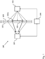
- FIG. 1 shows a diagram in the form of a schematic side view (partially in cross section) of an inspection device 100 for verifying a semifinished product 101 with a limited by an edge 103 a recess.
- the recess is designed, for example, to receive an electronic circuit 104 in the form of a chip or chip module within the scope of smart card production.
- the semifinished product 101 which is also referred to as an inlay, comprises a carrier foil 102 and a compensating foil 103.
- the electronic circuit 104 is fastened to the carrier foil 102 by means of an adhesive, for example.
- the recess bounded by the edge 103a is located in the balance sheet 103 to receive the electronic circuit 104.
- the carrier foil 102 and / or the compensating foil 103 may consist of a plastic material, in particular of PC, PVC, ABS or PET.
- the inspection device 100 shown comprises an illumination source 105, which is designed to illuminate the semifinished product 101 and the edge 103a formed therein with light of a predetermined wavelength, as shown in FIG FIG. 1 is shown schematically.
- the illumination source 105 is designed to illuminate the semifinished product 101 and the edge 103a formed therein with UV light.
- the inspection apparatus 100 further comprises an image camera 107, which is designed to capture an image recording of the illuminated semifinished product 101 with the recess bounded by the edge 103a.
- the semifinished product 101 can be arranged between the illumination source 105 and the image camera 107.
- the illumination source 105 and the image camera 107 can be arranged on the same side of the semifinished product 101.
- the image camera 107 may in particular be a digital image camera. According to one embodiment, the image camera 107 is designed to detect the image recording of the illuminated semifinished product 101 with the recess defined by the edge 103a in the UV light.
- the inspection device 100 further comprises a processor 109, which is designed to detect in the image acquisition by means of a Laplace image processing filter a profile of the edge 103a as a circumferential region and to verify the semifinished product 101 on the basis of the detected profile of the edge 103a.
- a Laplace image processing filter is a discrete approximation of the Laplacian operator.
- the processor 109 may be part of a computer (not shown) which may include a display for displaying the image captured by the imaging camera 107 and optionally further processed by the processor 109.
- the edge 103a is a laser cutting edge.
- the edge 103a may be a punched edge.
- the processor 109 is configured to detect, in the image pickup by the Laplace filter, the shape of the edge 103a as a circumferential area having a light intensity which is larger than a light intensity of an area outside the circumferential area in the captured image pickup ,
- the processor 109 of the inspection device 100 is configured within a light intensity range, in particular gray scale range, Detecting pixels in the captured image to capture the surrounding area.
- the processor 109 is configured to replace the light intensity preferably by the maximum light intensity (eg to the normalized maximum light intensity 1) before the detection of the circumferential area in the captured image pickup for pixels whose light intensity is greater than a first threshold value, and for pixels whose light intensity is less than the first threshold, it is preferable to replace the light intensity with the minimum light intensity (eg, normalized minimum light intensity 0).
- the minimum light intensity eg, normalized minimum light intensity 0
- the processor 109 is formed prior to detection of the circumferential area in the captured image pickup at pixels whose light intensity is greater than the first threshold and the one contiguous area form, the area of which is smaller than a second threshold, preferably to replace the light intensity by the minimum light intensity (eg by the normalized minimum light intensity 0).
- the processor 109 is configured to detect, prior to the detection of the circumferential area in the captured image pick-up, pixels within the detected image area within the detected circumferential area, i. within the course of the edge 103a, the light intensity is replaced by the minimum light intensity (e.g., by the normalized minimum light intensity 0).
- the minimum light intensity e.g., by the normalized minimum light intensity 0.
- the processor 109 may be configured to perform a contrast enhancement in the acquired image acquisition.
- the processor 109 may be formed, prior to the detection of the circumferential area in the captured image recording at adjacent pixels whose light intensities are more as a predefined threshold, to replace the light intensities preferably by maximum light intensities.
- the processor 109 is designed to align or center the circulating region or the course of the laser cutting edge 103 in the acquired image recording on the basis of a pattern profile.
- the processor 109 may be configured to define the pattern profile on the basis of the course of the laser cutting edge of a card body already verified by the inspection device 100.
- the processor 109 is embodied in accordance with one embodiment detected image acquisition based on the detected circumferential area to determine a center of the detected circumferential area or the course of the edge 103 a.
- the detected circumferential area in the captured image pickup is substantially rectangular, wherein the processor 109 is further configured to determine edge intersections of adjacent edges of the rectangular circumferential area in the captured image pickup, around the midpoint of the rectangular circumferential area to determine the edge 103a.
- the center point of the rectangular peripheral area or the course of the edge 103a can be determined by determining the intersection of the diagonals connecting the edge intersections.
- the processor 109 may be configured to advance in the captured image capture from the midpoint of the edge 103a, preferably pixel by pixel, ie, pixel by pixel, preferably horizontally and vertically in both the positive and negative directions until after If a pixel has been passed whose light intensity is greater than a predefined third threshold, the light intensity of the corresponding pixel of the captured image capture is less than a predefined fourth threshold, the third threshold being greater than the fourth threshold.
- Hiertig can be determined very accurately the outer edge of the peripheral region of higher light intensity in the captured image recording.
- this algorithm ends in the captured image capture at the latest at the "noisy" compensating film 103, which surrounds the edge 103, whereby the resulting measurement error can be minimized.
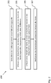
- FIG. 2 shows a schematic diagram of a method 200 for verifying a card body 101 having a limited by a laser cutting edge 103 recess for receiving an electronic circuit.
- the method 200 includes illuminating 201 of the card body 101 with light of a predetermined wavelength by means of a lighting source 105; detecting 203 an image capture of the illuminated card body 101 with the limited by the edge 103 recess by means of an image camera 107; detecting 205 a circumferential area having a light intensity in the captured image pickup which is greater than a light intensity of a region outside the circumferential area in the captured image pickup to determine the shape of the edge 103 in the captured image pickup; and verifying 207 the map body 101 based on the course of the edge 103.
Landscapes
- Engineering & Computer Science (AREA)
- General Physics & Mathematics (AREA)
- Physics & Mathematics (AREA)
- Theoretical Computer Science (AREA)
- Computer Vision & Pattern Recognition (AREA)
- Analytical Chemistry (AREA)
- General Health & Medical Sciences (AREA)
- Biochemistry (AREA)
- Immunology (AREA)
- Pathology (AREA)
- Chemical & Material Sciences (AREA)
- Quality & Reliability (AREA)
- Life Sciences & Earth Sciences (AREA)
- Health & Medical Sciences (AREA)
- Image Analysis (AREA)
- Investigating Materials By The Use Of Optical Means Adapted For Particular Applications (AREA)
Abstract
Description
- Die vorliegende Erfindung betrifft eine Inspektionsvorrichtung und ein Verfahren zum Verifizieren eines Halbzeugs zum Herstellen einer Chipkarte mit einer durch eine Kante begrenzten Aussparung zur Aufnahme eines elektronischen Schaltkreises in Form eines Chips oder Chipmoduls.
- Moderne elektronische Identifikationsdokumente, beispielsweise elektronische Personalausweise, sind oftmals in Form einer Chipkarte ausgebildet. Chipkarten können ferner als Kreditkarten, Bankkarten, elektronische Börsen usw. ausgebildet sein und zur bargeldlosen Abwicklung von Transaktionen, wie beispielsweise zum Entrichten eines Beförderungsentgelts im Personennahverkehr oder zum Bezahlen eines Kaufpreises für eine Ware oder Dienstleistung, dienen.
- Eine Chipkarte umfasst in der Regel einen Kartenkörper und einen in den Kartenkörper integrierten elektronischen Schaltkreis in Form eines Chips oder Chipmoduls, der zur Speicherung, Verarbeitung und/oder Erkennung von Informationen ausgebildet ist, die kontaktlos und/oder kontaktbehaftet mit einem Lesegerät ausgetauscht werden können.
- Üblicherweise besteht der Kartenkörper einer Chipkarte aus mehreren Folien oder Lagen aus Kunststoff. Aus der
WO2011/003518 und derDE102011001722 sind beispielhafte Herstellungsverfahren bekannt, bei denen ein auf einer Trägerfolie beispielsweise mittels Klebstoff befestigter elektronischer Schaltkreis in Form eines Chips oder Chipmoduls passgenau in eine Aussparung eingebracht wird, die in einer sogenannten Ausgleichsfolie ausgebildet ist. Dabei kann insbesondere bei Chipkarten, die kontaktlos mit einem Lesegerät kommunizieren, die Trägerfolie eine Antennenstruktur umfassen, die mit dem elektronischen Schaltkreis elektrisch verbunden ist. - Oftmals wird die Aussparung zur Aufnahme des elektronischen Schaltkreises in der Ausgleichsfolie mittels Laserschneiden erzeugt. Die Aussparung kann jedoch auch beispielsweise durch ein Ausstanzen erzeugt werden. Zur Fertigstellung einer Chipkarte können eine oder mehrere weitere Folien bzw. Lagen auf die Ober- und/oder Unterseite des aus Trägerfolie, Chip und Ausgleichsfolie bestehenden Halbzeugs, das auch als Inlay bezeichnet wird, laminiert werden, um den elektronischen Schaltkreis in den dadurch entstehenden Kartenkörper einzubetten.
- Fehler bei der Ausrichtung und Anordnung des elektronischen Schaltkreises relativ zu der Aussparung können dazu führen, dass die fertiggestellte Chipkarte von vornherein nicht funktionsfähig ist oder unter den normalen Einflüssen, denen eine Chipkarte beim Einsatz ausgesetzt ist, nach kurzer Zeit im Feld ihre Funktionsfähigkeit verliert.
- Daher besteht eine Aufgabe der vorliegenden Erfindung darin, ein Konzept zum automatisierten Verifizieren eines Chipkartenhalbzeugs mit einer Aussparung zur Aufnahme eines elektronischen Schaltkreises in Form eines Chips oder Chipmoduls zu schaffen, um insbesondere die vorstehend beschriebenen Probleme bei der Herstellung von Chipkarten vermeiden zu können.
- Diese Aufgabe wird durch die Merkmale der unabhängigen Ansprüche gelöst. Vorteilhafte Ausbildungsformen sind Gegenstand der abhängigen Patentansprüche, der Beschreibung sowie der Figuren.
- Überraschenderweise hat sich herausgestellt, dass sich bei einem Chipkartenhalbzeug die Ausrichtung und/oder Anordnung des elektronischen Schaltkreises relativ zu der Aussparung des Chipkartenhalbzeugs besonders gut dadurch bestimmen lässt, dass mittels eines Laplace-Bildverarbeitungsfilters in einer Bildaufnahme des Chipkartenhalbzeugs der Verlauf der Kante bestimmt wird, durch welche die Aussparung begrenzt wird.
- Somit betrifft die Erfindung gemäß einem ersten Aspekt eine Inspektionsvorrichtung zum Verifizieren eines Halbzeugs zum Herstellen einer Chipkarte mit einer durch eine Kante begrenzten Aussparung zur Aufnahme eines elektronischen Schaltkreises. Die Inspektionsvorrichtung umfasst eine Beleuchtungsquelle, welche ausgebildet ist, das Halbzeug mit Licht einer vorbestimmten Wellenlänge zu beleuchten, eine Bildkamera, welche ausgebildet ist, eine Bildaufnahme des beleuchteten Halbzeugs mit der durch die Kante begrenzten Aussparung zu erfassen, und einen Prozessor, welcher ausgebildet ist, in der Bildaufnahme mittels eines Laplace-Filters einen Verlauf der Kante als einen umlaufenden Bereich zu erfassen und das Halbzeug auf der Grundlage des erfassten Verlaufs der Kante zu verifizieren.
- Dadurch wird ein effizientes Konzept zum automatisierten Verifizieren eines Halbzeugs zum Herstellen einer Chipkarte mit einer durch eine Kante begrenzten Aussparung zur Aufnahme eines elektronischen Schaltkreises in Form eines Chips oder Chipmoduls geschaffen.
- Gemäß einer Ausführungsform handelt es sich bei der Kante um eine Laserschneidkante. Alternativ kann die Kante eine ausgestanzte Kante sein.
- Gemäß einer Ausführungsform ist der Prozessor ausgebildet, in der Bildaufnahme mittels des Laplace-Filters den Verlauf der Kante als einen umlaufenden Bereich mit einer Lichtintensität zu erfassen, welche größer als eine Lichtintensität eines in der erfassten Bildaufnahme außerhalb des umlaufenden Bereichs liegenden Bereichs ist.
- Gemäß einer Ausführungsform ist die Beleuchtungsquelle ausgebildet, das Halbzeug mit UV-Licht zu beleuchten, oder die Bildkamera ausgebildet, die Bildaufnahme im UV-Licht zu erfassen.
- Dadurch wird beispielsweise der Vorteil erreicht, dass der Kontrast zwischen dem umlaufenden Bereich und benachbarten Bereichen in der erfassten Bildaufnahme verstärkt wird und sich somit der umlaufende Bereich besser automatisiert erfassen lässt.
- Gemäß einer Ausführungsform ist der Prozessor ausgebildet, innerhalb eines Lichtintensitätsbereichs, insbesondere Graustufenbereichs, liegende Pixel in der erfassten Bildaufnahme zu erfassen, um den umlaufenden Bereich zu erfassen.
- Dadurch wird beispielsweise der Vorteil erreicht, dass die Analyse und/oder Verarbeitung der Bildaufnahme durch den Prozessor effizienter durchgeführt werden kann.
- Gemäß einer Ausführungsform ist der Prozessor ausgebildet, vor der Erfassung des umlaufenden Bereichs in der erfassten Bildaufnahme bei Pixeln, deren Lichtintensität größer als ein erster Schwellenwert ist, die Lichtintensität durch einen erste, insbesondere maximale, Lichtintensität zu ersetzen, die größer als der erste Schwellenwert ist, und bei Pixeln, deren Lichtintensität kleiner als der erste Schwellenwert ist, die Lichtintensität durch eine zweite, insbesondere minimale, Lichtintensität zu ersetzen, die kleiner als der erste Schwellenwert ist.
- Durch eine derartige Binarisierung der erfassten Bildaufnahme wird beispielsweise der Vorteil erreicht, dass der umlaufende Bereich effizienter erfasst werden kann.
- Gemäß einer Ausführungsform ist der Prozessor ausgebildet, vor der Erfassung des umlaufenden Bereichs in der erfassten Bildaufnahme bei Pixeln, deren Lichtintensität größer als der erste Schwellenwert ist und die einen zusammenhängenden Bereich ausbilden, dessen Fläche kleiner als ein zweiter Schwellenwert ist, die Lichtintensität durch die zweite, insbesondere minimale, Lichtintensität zu ersetzen.
- Dadurch wird beispielsweise der Vorteil erreicht, dass Rauschartefakte in der erfassten Bildaufnahme entfernt werden können, was das Erfassen des umlaufenden Bereichs in der Bildaufnahme erleichtert.
- Gemäß einer Ausführungsform ist der Prozessor ausgebildet, vor der Erfassung des umlaufenden Bereichs in der erfassten Bildaufnahme bei Pixeln, die in der erfassten Bildaufnahme innerhalb des Verlaufs der Kante liegen, die Lichtintensität durch eine minimale Lichtintensität zu ersetzen.
- Dadurch wird beispielsweise der Vorteil erreicht, dass die durch die Kante begrenzte Aussparung in der erfassten Bildaufnahme ausgeblendet werden kann, was das Erfassen des umlaufenden Bereichs in der Bildaufnahme erleichtert.
- Gemäß einer Ausführungsform ist der Prozessor ausgebildet, in der erfassten Bildaufnahme den Verlauf der Kante anhand eines Musterverlaufs auszurichten oder zu zentrieren.
- Dabei kann der Prozessor ausgebildet sein, den Musterverlauf auf der Grundlage des Verlaufs der Kante eines bereits verifizierten Halbzeugs zu definieren. Dadurch wird beispielsweise der Vorteil erreicht, dass der umlaufende Bereich in der Bildaufnahme effizienter erfasst werden kann.
- Gemäß einer Ausführungsform ist der Prozessor ausgebildet, in der erfassten Bildaufnahme auf der Grundlage des erfassten umlaufenden Bereichs einen Mittelpunkt des Verlaufs der Kante zu bestimmen.
- Dadurch wird beispielsweise der Vorteil erreicht, dass die Analyse und/oder Verarbeitung der Bildaufnahme durch den Prozessor effizienter durchgeführt werden kann.
- Gemäß einer Ausführungsform ist in der erfassten Bildaufnahme der erfasste umlaufende Bereich im Wesentlichen rechteckig und der Prozessor ist ausgebildet, in der erfassten Bildaufnahme Schnittpunkte von benachbarten Kanten des rechteckigen umlaufenden Bereichs zu bestimmen, um den Mittelpunkt des Verlaufs der Kante zu bestimmen.
- Gemäß einer Ausführungsform ist der Prozessor ausgebildet, in der erfassten Bildaufnahme vom Mittelpunkt des Verlaufs der Kante solange pixelweise voranzuschreiten, bis, nachdem ein Pixel passiert worden ist, dessen Lichtintensität größer als ein dritter Schwellenwert ist, die Lichtintensität eines Pixels kleiner als ein vierter Schwellenwert ist. Dadurch wird beispielsweise der Vorteil erreicht, dass sich auf einfache Art und Weise die Größe, die Anordnung oder die Ausrichtung der durch die Kante begrenzten Aussparung bestimmen lässt, die zur Verifizierung des Halbzeugs herangezogen werden können.
- Gemäß einer Ausführungsform ist der Prozessor ausgebildet, in der erfassten Bildaufnahme vom Mittelpunkt des Verlaufs der Kante horizontal und vertikal sowohl in positiver als auch in negativer Richtung solange pixelweise voranzuschreiten, bis, nachdem jeweils ein Pixel passiert worden ist, dessen Lichtintensität größer als ein dritter Schwellenwert ist, die Lichtintensität eines Pixels kleiner als ein vierter Schwellenwert ist. Dadurch wird beispielsweise der Vorteil erreicht, dass sich auf einfache Art und Weise die Größe, die Anordnung oder die Ausrichtung der durch die Kante begrenzten Aussparung bestimmen lässt, die zur Verifizierung des Halbzeugs herangezogen werden können.
- Gemäß einem zweiten Aspekt betrifft die Erfindung ein Verfahren zum Verifizieren eines Halbzeugs mit einer durch eine Kante begrenzten Aussparung zur Aufnahme eines elektronischen Schaltkreises. Dabei umfasst das Verfahren das Beleuchten des Halbzeugs mit Licht einer vorbestimmten Wellenlänge mittels einer Beleuchtungsquelle, das Erfassen einer Bildaufnahme des beleuchteten Halbzeugs mit der durch die Kante begrenzten Aussparung mittels einer Bildkamera; das Erfassen eines Verlaufs der Kante mittels eines Laplace-Filters als einen umlaufenden Bereich in der Bildaufnahme und das Verifizieren des Halbzeugs auf der Grundlage des erfassten Verlaufs der Kante.
- Die Inspektionsvorrichtung gemäß dem ersten Aspekt der Erfindung ist dazu ausgebildet, das Verfahren gemäß dem zweiten Aspekt der Erfindung auszuführen. Weitere Ausführungsformen des Verfahrens gemäß dem zweiten Aspekt der Erfindung ergeben sich aus den vorstehend beschriebenen Ausführungsformen der Inspektionsvorrichtung gemäß dem ersten Aspekt der Erfindung.
- Die Erfindung kann in Hardware und/oder Software realisiert werden.
- Weitere Ausführungsbeispiele werden Bezug nehmend auf die beiliegenden Figuren näher erläutert. Es zeigen:
- Fig. 1
- ein schematisches Diagramm einer Inspektionsvorrichtung zum Verifizieren eines Chipkartenhalbzeugs mit einer Aussparung zur Aufnahme eines elektronischen Schaltkreises gemäß einer Ausführungsform; und
- Fig. 2
- ein Diagramm mit den Schritten eines Verfahrens zum Verifizieren eines Kartenkörpers mit einer Aussparung zur Aufnahme eines elektronischen Schaltkreises gemäß einer Ausführungsform.
-
Figur 1 zeigt ein Diagramm in Form einer schematischen Seitenansicht (teilweise im Querschnitt) einer Inspektionsvorrichtung 100 zum Verifizieren eines Halbzeugs 101 mit einer durch eine Kante 103a begrenzten Aussparung. Die Aussparung ist dazu ausgebildet, beispielsweise im Rahmen der Chipkartenherstellung einen elektronischen Schaltkreis 104 in Form eines Chips oder Chipmoduls aufzunehmen. - Bei der in
Figur 1 gezeigten Ausführungsform umfasst das Halbzeug 101, das auch als Inlay bezeichnet wird, eine Trägerfolie 102 und eine Ausgleichsfolie 103. Der elektronische Schaltkreis 104 ist beispielsweise mittels eines Klebstoffs auf der Trägerfolie 102 befestigt. Die durch die Kante 103a begrenzte Aussparung befindet sich in der Ausgleichsfolie 103, um den elektronischen Schaltkreis 104 aufzunehmen. Die Trägerfolie 102 und/oder die Ausgleichsfolie 103 können aus einem Kunststoffmaterial, insbesondere aus PC, PVC, ABS oder PET, bestehen. - Die in
Figur 1 dargestellte Inspektionsvorrichtung 100 umfasst eine Beleuchtungsquelle 105, welche ausgebildet ist, das Halbzeug 101 und die darin ausgebildete Kante 103a mit Licht einer vorbestimmten Wellenlänge zu beleuchten, wie dies inFigur 1 schematisch dargestellt ist. Gemäß einer Ausführungsform ist die Beleuchtungsquelle 105 ausgebildet, das Halbzeug 101 sowie die darin ausgebildete Kante 103a mit UV-Licht zu beleuchten. Die Inspektionsvorrichtung 100 umfasst ferner eine Bildkamera 107, welche ausgebildet ist, eine Bildaufnahme des beleuchteten Halbzeugs 101 mit der durch die Kante 103a begrenzten Aussparung zu erfassen. Hierzu kann das Halbzeug 101 zwischen der Beleuchtungsquelle 105 und der Bildkamera 107 angeordnet sein. Ebenso können die Beleuchtungsquelle 105 und die Bildkamera 107 auf derselben Seite des Halbzeugs 101 angeordnet sein. - Bei der Bildkamera 107 kann es sich insbesondere um eine Digitalbildkamera handeln. Gemäß einer Ausführungsform ist die Bildkamera 107 ausgebildet, die Bildaufnahme des beleuchteten Halbzeugs 101 mit der durch die Kante 103a begrenzten Aussparung im UV-Licht zu erfassen.
- Die Inspektionsvorrichtung 100 umfasst ferner einen Prozessor 109, welcher ausgebildet ist, in der Bildaufnahme mittels eines Laplace-Bildverarbeitungsfilters einen Verlauf der Kante 103a als einen umlaufenden Bereich zu erfassen und das Halbzeug 101 auf der Grundlage des erfassten Verlaufs der Kante 103a zu verifizieren. Ein Laplace-Bildverarbeitungsfilter ist eine diskrete Approximation des Laplace-Operators.
- Der Prozessor 109 kann Teil eines Computers (nicht dargestellt) sein, der ein Display zur Anzeige der von der Bildkamera 107 erfassten und vom Prozessor 109 gegebenenfalls weiter verarbeiteten Bildaufnahme umfassen kann.
- Gemäß einer Ausführungsform handelt es sich bei der Kante 103a um eine Laserschneidkante. Alternativ kann die Kante 103a eine ausgestanzte Kante sein. Insbesondere im Fall einer Laserschneidkante 103a hat es sich gezeigt, dass bei der Bestrahlung des Halbzeugs 101 mittels der Beleuchtungsquelle 105 mit UV-Licht und der entsprechenden Erfassung der Bildaufnahme des Halbzeugs mittels der Bildkamera 107 im UV-Licht, die Kante 103a als umlaufender Bereich erhöhter Lichtintensität deutlich hervortritt. Dementsprechend ist der Prozessor 109 gemäß einer Ausführungsform ausgebildet, in der Bildaufnahme mittels des Laplace-Filters den Verlauf der Kante 103a als einen umlaufenden Bereich mit einer Lichtintensität zu erfassen, welche größer als eine Lichtintensität eines in der erfassten Bildaufnahme außerhalb des umlaufenden Bereichs liegenden Bereichs ist.
- Gemäß einer Ausführungsform ist der Prozessor 109 der Inspektionsvorrichtung 100 ausgebildet, innerhalb eines Lichtintensitätsbereichs, insbesondere Graustufenbereichs, liegende Pixel in der erfassten Bildaufnahme zu erfassen, um den umlaufenden Bereich zu erfassen.
- Gemäß einer Ausführungsform ist der Prozessor 109 ausgebildet, vor der Erfassung des umlaufenden Bereichs in der erfassten Bildaufnahme bei Pixeln, deren Lichtintensität größer als ein erster Schwellenwert ist, die Lichtintensität vorzugsweise durch die maximale Lichtintensität zu ersetzen (z.B. auf die normierte maximale Lichtintensität 1), und bei Pixeln, deren Lichtintensität kleiner als der erste Schwellenwert ist, die Lichtintensität vorzugsweise durch die minimale Lichtintensität (z.B. auf die normierte minimale Lichtintensität 0) zu ersetzen. Mittels einer derartigen "Binarisierung" der Bildaufnahme durch den Prozessor 109, kann der umlaufende Bereich in der binarisierten Bildaufnahme effizienter erfasst werden.
- Zur Verminderung von Rauschartefakten in der Bildaufnahme außerhalb der durch die Kante 103 begrenzten Aussparung ist gemäß einer Ausführungsform der Prozessor 109 ausgebildet, vor der Erfassung des umlaufenden Bereichs in der erfassten Bildaufnahme bei Pixeln, deren Lichtintensität größer als der erste Schwellenwert ist und die einen zusammenhängenden Bereich ausbilden, dessen Fläche kleiner als ein zweiter Schwellenwert ist, die Lichtintensität vorzugsweise durch die minimale Lichtintensität (z.B. durch die normierte minimale Lichtintensität 0) zu ersetzen.
- Zur Ausblendung der durch die Kante 103a begrenzten Aussparung in der erfassten Bildaufnahme ist gemäß einer Ausführungsform der Prozessor 109 ausgebildet, vor der Erfassung des umlaufenden Bereichs in der erfassten Bildaufnahme bei Pixeln, die in der erfassten Bildaufnahme innerhalb des erfassten umlaufenden Bereichs liegen, d.h. innerhalb des Verlaufs der Kante 103a liegen, die Lichtintensität durch die minimale Lichtintensität (z.B. durch die normierte minimale Lichtintensität 0) zu ersetzen. Durch die Ausblendung der durch die Kante 103a begrenzten Aussparung in der erfassten Bildaufnahme kann das Erfassen des umlaufenden Bereichs in der Bildaufnahme erleichtert werden.
- Ferner kann gemäß einer Ausführungsform der Prozessor 109 ausgebildet sein, in der erfassten Bildaufnahme eine Kontrastverstärkung durchzuführen. Hierzu kann der Prozessor 109 ausgebildet sein, vor der Erfassung des umlaufenden Bereichs in der erfassten Bildaufnahme bei benachbarten Pixeln, deren Lichtintensitäten sich um mehr als einen vordefinierten Schwellenwert unterscheiden, die Lichtintensitäten vorzugsweise durch maximale Lichtintensitäten zu ersetzen.
- Gemäß einer Ausführungsform ist der Prozessor 109 ausgebildet, in der erfassten Bildaufnahme den umlaufenden Bereich bzw. den Verlauf der Laserschneidkante 103 anhand eines Musterverlaufs auszurichten oder zu zentrieren. Dabei kann der Prozessor 109 ausgebildet sein, den Musterverlauf auf der Grundlage des Verlaufs der Laserschneidkante eines bereits durch die Inspektionsvorrichtung 100 verifizierten Kartenkörpers zu definieren.
- Zur genauen Bestimmung der Größe, Anordnung und/oder Ausrichtung des umlaufenden Bereichs bzw. der durch die Kante 103a begrenzten Aussparung in der erfassten Bildaufnahme, die ebenfalls zur Verifizierung des Halbzeugs 101 herangezogen werden kann, ist gemäß einer Ausführungsform der Prozessor 109 ausgebildet, in der erfassten Bildaufnahme auf der Grundlage des erfassten umlaufenden Bereichs einen Mittelpunkt des erfassten umlaufenden Bereichs bzw. des Verlaufs der Kante 103a zu bestimmen. Gemäß einer Ausführungsform ist der erfasste umlaufende Bereich in der erfassten Bildaufnahme im Wesentlichen rechteckig, wobei der Prozessor 109 ferner ausgebildet ist, in der erfassten Bildaufnahme Kantenschnittpunkte von benachbarten Kanten des rechteckigen umlaufenden Bereichs zu bestimmen, um den Mittelpunkt des rechteckigen umlaufenden Bereichs bzw. des Verlaufs der Kante 103a zu bestimmen. Der Mittelpunkt des rechteckigen umlaufenden Bereichs bzw. des Verlaufs der Kante 103a lässt sich beispielsweise bestimmen, indem der Schnittpunkt der Diagonalen bestimmt wird, welche die Kantenschnittpunkte miteinander verbinden.
- Ferner kann der Prozessor 109 ausgebildet sein, in der erfassten Bildaufnahme vom Mittelpunkt des Verlaufs der Kante 103a solange vorzugsweise pixelweise, d.h. Pixel für Pixel, voranzuschreiten, und zwar vorzugsweise horizontal und vertikal sowohl in positiver als auch in negativer Richtung, bis, nachdem auf diese Weise ein Pixel passiert worden ist, dessen Lichtintensität größer als ein vordefinierter dritter Schwellenwert ist, die Lichtintensität des entsprechenden Pixels der erfassten Bildaufnahme kleiner als ein vordefinierter vierter Schwellenwert ist, wobei der dritte Schwellenwert größer als der vierte Schwellenwert ist. Hierdruck kann sehr genau der äußere Rand des umlaufenden Bereichs höherer Lichtintensität in der erfassten Bildaufnahme bestimmt werden. Für den Fall, dass der äußere Rand des umlaufenden Bereichs höherer Lichtintensität in der erfassten Bildaufnahme nicht gut zu erkennen ist, endet dieser Algorithmus in der erfassten Bildaufnahme spätestens bei dem "verrauschten" Ausgleichsfolie 103, welche die Kante 103 umgibt, wodurch der entstehende Messfehler auf ein Mindestmaß beschränkt werden kann.
-
Figur 2 zeigt ein schematisches Diagramm eines Verfahrens 200 zum Verifizieren eines Kartenkörpers 101 mit einer durch eine Laserschneidkante 103 begrenzten Aussparung zur Aufnahme eines elektronischen Schaltkreises. Dabei umfasst das Verfahren 200 das Beleuchten 201 des Kartenkörpers 101 mit Licht einer vorbestimmten Wellenlänge mittels einer Beleuchtungsquelle 105; das Erfassen 203 einer Bildaufnahme des beleuchteten Kartenkörpers 101 mit der durch die Kante 103 begrenzten Aussparung mittels einer Bildkamera 107; das Erfassen 205 eines umlaufenden Bereichs mit einer Lichtintensität in der erfassten Bildaufnahme, welche größer als eine Lichtintensität eines in der erfassten Bildaufnahme außerhalb des umlaufenden Bereichs liegenden Bereichs ist, um den Verlauf der Kante 103 in der erfassten Bildaufnahme zu bestimmen; und das Verifizieren 207 des Kartenkörpers 101 auf der Grundlage des Verlaufs der Kante 103. -
- 100
- Inspektionsvorrichtung
- 101
- Halbzeug
- 102
- Trägerfolie
- 103
- Ausgleichsfolie
- 103a
- Aussparungskante
- 104
- elektronischer Schaltkreis
- 105
- Beleuchtungsquelle
- 107
- Bildkamera
- 109
- Prozessor
- 200
- Verfahren zum Verifizieren eines Halbzeugs
- 201
- Beleuchten des Halbzeugs
- 203
- Erfassen einer Bildaufnahme des Halbzeugs
- 205
- Erfassen eines Verlaufs einer Aussparungskante
- 207
- Verifizieren des Halbzeugs
Claims (15)
- Inspektionsvorrichtung (100) zum Verifizieren eines Halbzeugs (101) zum Herstellen einer Chipkarte mit einer durch eine Kante (103a) begrenzten Aussparung zur Aufnahme eines elektronischen Schaltkreises (104) mit:einer Beleuchtungsquelle (105), welche ausgebildet ist, das Halbzeug (101) mit Licht einer vorbestimmten Wellenlänge zu beleuchten;einer Bildkamera (107), welche ausgebildet ist, eine Bildaufnahme des beleuchteten Halbzeugs (101) mit der durch die Kante (103a) begrenzten Aussparung zu erfassen; undeinem Prozessor (109), welcher ausgebildet ist, mittels eines Laplace-Filters einen Verlauf der Kante (103a) in der Bildaufnahme als einen umlaufenden Bereich zu erfassen und das Halbzeug (101) auf der Grundlage des erfassten Verlaufs der Kante (103a) zu verifizieren.
- Inspektionsvorrichtung (100) nach Anspruch 1, wobei die Kante (103a) eine Laserschneidkante ist.
- Inspektionsvorrichtung (100) nach Anspruch 2, wobei der Prozessor (109) ausgebildet ist, in der Bildaufnahme mittels des Laplace-Filters den Verlauf der Kante (103a) als einen umlaufenden Bereich mit einer Lichtintensität zu erfassen, welche größer als eine Lichtintensität eines in der erfassten Bildaufnahme außerhalb des umlaufenden Bereichs liegenden Bereichs ist.
- Inspektionsvorrichtung (100) nach Anspruch 3, wobei die Beleuchtungsquelle (105) ausgebildet ist, das Halbzeug (101) mit UV-Licht zu beleuchten, oder die Bildkamera (107) ausgebildet ist, die Bildaufnahme im UV-Licht zu erfassen.
- Inspektionsvorrichtung (100) nach einem der vorstehenden Ansprüche, wobei der Prozessor (109) ausgebildet ist, innerhalb eines Lichtintensitätsbereichs, insbesondere Graustufenbereichs, liegende Pixel in der erfassten Bildaufnahme zu erfassen, um den umlaufenden Bereich zu erfassen.
- Inspektionsvorrichtung (100) nach einem der vorstehenden Ansprüche, wobei der Prozessor (109) ausgebildet ist, vor der Erfassung des umlaufenden Bereichs in der erfassten Bildaufnahme bei Pixeln, deren Lichtintensität größer als ein erster Schwellenwert ist, die Lichtintensität durch einen erste, insbesondere maximale, Lichtintensität zu ersetzen, die größer als der erste Schwellenwert ist, und bei Pixeln, deren Lichtintensität kleiner als der erste Schwellenwert ist, die Lichtintensität durch eine zweite, insbesondere minimale, Lichtintensität zu ersetzen, die kleiner als der erste Schwellenwert ist.
- Inspektionsvorrichtung (100) nach Anspruch 6, wobei der Prozessor (109) ausgebildet ist, vor der Erfassung des umlaufenden Bereichs in der erfassten Bildaufnahme bei Pixeln, deren Lichtintensität größer als der erste Schwellenwert ist und die einen zusammenhängenden Bereich ausbilden, dessen Fläche kleiner als ein zweiter Schwellenwert ist, die Lichtintensität durch die zweite, insbesondere minimale, Lichtintensität zu ersetzen.
- Inspektionsvorrichtung (100) nach einem der vorstehenden Ansprüche, wobei der Prozessor (109) ausgebildet ist, vor der Erfassung des umlaufenden Bereichs in der erfassten Bildaufnahme bei Pixeln, die in der erfassten Bildaufnahme innerhalb des Verlaufs der Kante (103a) liegen, die Lichtintensität durch eine minimale Lichtintensität zu ersetzen.
- Inspektionsvorrichtung (100) nach einem der vorstehenden Ansprüche, wobei der Prozessor (109) ausgebildet ist, in der erfassten Bildaufnahme den Verlauf der Kante (103a) anhand eines Musterverlaufs auszurichten oder zu zentrieren.
- Inspektionsvorrichtung (100) nach einem der vorstehenden Ansprüche, wobei der Prozessor (109) ausgebildet ist, in der erfassten Bildaufnahme auf der Grundlage des erfassten umlaufenden Bereichs einen Mittelpunkt des Verlaufs der Kante (103a) zu bestimmen.
- Inspektionsvorrichtung (100) nach Anspruch 10, wobei in der erfassten Bildaufnahme der erfasste umlaufende Bereich im Wesentlichen rechteckig ist und wobei der Prozessor (109) ausgebildet ist, in der erfassten Bildaufnahme Schnittpunkte von benachbarten Kanten des rechteckigen umlaufenden Bereichs zu bestimmen, um den Mittelpunkt des Verlaufs der Kante (103a) zu bestimmen.
- Inspektionsvorrichtung (100) nach Anspruch 10 oder 11, wobei der Prozessor (109) ausgebildet ist, in der erfassten Bildaufnahme vom Mittelpunkt des Verlaufs der Kante (103a) solange pixelweise voranzuschreiten, bis, nachdem ein Pixel passiert worden ist, dessen Lichtintensität größer als ein dritter Schwellenwert ist, die Lichtintensität eines Pixels kleiner als ein vierter Schwellenwert ist.
- Inspektionsvorrichtung (100) nach Anspruch 12, wobei der Prozessor (109) ausgebildet ist, in der erfassten Bildaufnahme vom Mittelpunkt des Verlaufs der Kante horizontal und vertikal in positiver und negativer Richtung solange pixelweise voranzuschreiten, bis, nachdem jeweils ein Pixel passiert worden ist, dessen Lichtintensität größer als ein dritter Schwellenwert ist, die Lichtintensität eines Pixels kleiner als ein vierter Schwellenwert ist.
- Verfahren (200) zum Verifizieren eines Halbzeugs (101) mit einer durch eine Kante (103a) begrenzten Aussparung zur Aufnahme eines elektronischen Schaltkreises (104) mit:Beleuchten (201) des Halbzeugs (101) mit Licht einer vorbestimmten Wellenlänge mittels einer Beleuchtungsquelle (105);Erfassen (203) einer Bildaufnahme des beleuchteten Halbzeugs (101) mit der durch die Kante (103a) begrenzten Aussparung mittels einer Bildkamera (107);Erfassen (205) eines Verlaufs der Kante (103a) mittels eines Laplace-Filters als einen umlaufenden Bereich in der Bildaufnahme; undVerifizieren (207) des Halbzeugs (101) auf der Grundlage des erfassten Verlaufs der Kante (103a).
- Computerprogramm mit einem Programmcode zum Ausführen des Verfahrens (200) nach Anspruch 14, wenn das Computerprogramm auf einem Computer ausgeführt wird.
Applications Claiming Priority (1)
| Application Number | Priority Date | Filing Date | Title |
|---|---|---|---|
| DE102015122729.0A DE102015122729B4 (de) | 2015-12-23 | 2015-12-23 | Inspektionsvorrichtung und Verfahren zum Verifizieren eines Chipkartenhalbzeugs |
Publications (2)
| Publication Number | Publication Date |
|---|---|
| EP3184998A1 true EP3184998A1 (de) | 2017-06-28 |
| EP3184998B1 EP3184998B1 (de) | 2021-01-27 |
Family
ID=57570777
Family Applications (1)
| Application Number | Title | Priority Date | Filing Date |
|---|---|---|---|
| EP16205217.9A Active EP3184998B1 (de) | 2015-12-23 | 2016-12-20 | Inspektionsvorrichtung und verfahren zum verifizieren eines chipkartenhalbzeugs |
Country Status (2)
| Country | Link |
|---|---|
| EP (1) | EP3184998B1 (de) |
| DE (1) | DE102015122729B4 (de) |
Citations (5)
| Publication number | Priority date | Publication date | Assignee | Title |
|---|---|---|---|---|
| US4390955A (en) * | 1978-09-28 | 1983-06-28 | Tokyo Shibaura Denki Kabushiki Kaisha | Position detecting system |
| CN1761286A (zh) * | 2005-11-03 | 2006-04-19 | 上海交通大学 | 用边缘检测、运动检测和中值滤波去除蚊式噪声的方法 |
| WO2011003518A1 (de) | 2009-07-09 | 2011-01-13 | Bundesdruckerei Gmbh | Verfahren und vorrichtung zur herstellung eines inlays für einen folienverbund sowie folienverbund mit inlay |
| DE102011001722A1 (de) | 2011-04-01 | 2012-10-04 | Bundesdruckerei Gmbh | Halbzeug zur Herstellung eines Chipkartenmoduls, Verfahren zur Herstellung des Halbzeuges sowie Verfahren zur Herstellung einer Chipkarte |
| EP2583826A1 (de) * | 2011-10-19 | 2013-04-24 | Giesecke & Devrient GmbH | Herstellung eines Inlays mit integriertem Regelkreis |
Family Cites Families (3)
| Publication number | Priority date | Publication date | Assignee | Title |
|---|---|---|---|---|
| DE19705170A1 (de) | 1997-02-11 | 1998-08-20 | Orga Kartensysteme Gmbh | Taschenfräsanlage für Chipkarten |
| DE19833103C1 (de) | 1998-07-23 | 1999-08-26 | Orga Kartensysteme Gmbh | Chipkarten, Verfahren zur Herstellung derselben, Zwischenerzeugnis sowie System zur Prüfung der Echtheit derart hergestellter Chipkarten |
| EP1598861A1 (de) * | 2004-05-19 | 2005-11-23 | Axalto S.A. | Methode und Apparatur zu Kalibrierung und Steuerung des Bestückens einer Chipkarte mit einem Chip |
-
2015
- 2015-12-23 DE DE102015122729.0A patent/DE102015122729B4/de not_active Withdrawn - After Issue
-
2016
- 2016-12-20 EP EP16205217.9A patent/EP3184998B1/de active Active
Patent Citations (5)
| Publication number | Priority date | Publication date | Assignee | Title |
|---|---|---|---|---|
| US4390955A (en) * | 1978-09-28 | 1983-06-28 | Tokyo Shibaura Denki Kabushiki Kaisha | Position detecting system |
| CN1761286A (zh) * | 2005-11-03 | 2006-04-19 | 上海交通大学 | 用边缘检测、运动检测和中值滤波去除蚊式噪声的方法 |
| WO2011003518A1 (de) | 2009-07-09 | 2011-01-13 | Bundesdruckerei Gmbh | Verfahren und vorrichtung zur herstellung eines inlays für einen folienverbund sowie folienverbund mit inlay |
| DE102011001722A1 (de) | 2011-04-01 | 2012-10-04 | Bundesdruckerei Gmbh | Halbzeug zur Herstellung eines Chipkartenmoduls, Verfahren zur Herstellung des Halbzeuges sowie Verfahren zur Herstellung einer Chipkarte |
| EP2583826A1 (de) * | 2011-10-19 | 2013-04-24 | Giesecke & Devrient GmbH | Herstellung eines Inlays mit integriertem Regelkreis |
Non-Patent Citations (1)
| Title |
|---|
| XIAODONG XIE ET AL: "An Adaptive Image Enhancement Technique Based on Image Characteristic", IMAGE AND SIGNAL PROCESSING, 2009. CISP '09. 2ND INTERNATIONAL CONGRESS ON, IEEE, PISCATAWAY, NJ, USA, 17 October 2009 (2009-10-17), pages 1 - 5, XP031553169, ISBN: 978-1-4244-4129-7 * |
Also Published As
| Publication number | Publication date |
|---|---|
| DE102015122729A1 (de) | 2017-06-29 |
| DE102015122729B4 (de) | 2018-09-13 |
| EP3184998B1 (de) | 2021-01-27 |
Similar Documents
| Publication | Publication Date | Title |
|---|---|---|
| WO2014080031A1 (de) | Vorrichtung zum auslesen einer magnetstreifen- und/oder chipkarte mit einer kamera zur detektion von eingeschobenen skimmingmodulen | |
| EP2577620A1 (de) | Vorrichtung zur echtheitsprüfung von wertdokumenten | |
| DE102020120887B4 (de) | Verfahren zum erfassen einer einhängeposition eines auflagestegs und flachbettwerkzeugmaschine | |
| EP4306322A1 (de) | Verfahren zur prüfung von tiefdruckzylindern und tiefdruckplatten | |
| EP3357043B1 (de) | Dokument und verfahren zum verifizieren eines dokuments | |
| EP3184997B1 (de) | Inspektionsvorrichtung und verfahren zum verifizieren eines chipkartenhalbzeugs | |
| DE102015122729B4 (de) | Inspektionsvorrichtung und Verfahren zum Verifizieren eines Chipkartenhalbzeugs | |
| EP3184999B1 (de) | Inspektionsvorrichtung und verfahren zum verifizieren einer klebstoffverbindung | |
| EP1845336A1 (de) | Verfahren zur optischen Erfassung von bewegten Objekten und Vorrichtung | |
| EP3184996B1 (de) | Inspektionsvorrichtung und verfahren zum verifizieren eines chipkartenhalbzeugs | |
| WO2012113864A2 (de) | Identifikationsvorrichtung und identifikationsausweis | |
| EP1897067B1 (de) | Verfahren und vorrichtung zur erkennung einer münze unter verwendung ihres prägebildes | |
| EP2394250B1 (de) | Verfahren und vorrichtung zum verifizieren von dokumenten unter verwendung einer wavelet-transformation | |
| EP4070294B1 (de) | Vorrichtung und verfahren zur bearbeitung von wertdokumenten, insbesondere banknoten, sowie wertdokumentbearbeitungssystem | |
| DE102017127318A1 (de) | Vorrichtung und Verfahren zum Lochen von Kraftfahrzeug-Kennzeichenschildern | |
| EP1567991B1 (de) | Verfahren und vorrichtung zur prüfung von wertdokumenten | |
| DE102013002375A1 (de) | Verfahren zur Kalibrierung einer Kamera eines Kraftfahrzeugs | |
| DE102023131282B3 (de) | Verfahren und Vorrichtung zum Prüfen eines Sicherheitselements für ein Sicherheitsdokument | |
| EP2899699B1 (de) | Verfahren zum Überprüfen der Echtheit eines Identifikationsdokumentes | |
| DE102021001256B3 (de) | Verfahren zum Erkennen eines Objekts in einem Suchbild, und Verwendung eines Verfahrens zur Bestimmung einer Position und/oder Orientierung eines Sicherheitselements einer Banknote | |
| WO2012150211A1 (de) | Verfahren und vorrichtung zum erkennen eines zeichens | |
| WO2013024161A1 (de) | Verfahren, vorrichtung und computerprogramm zur wiedererkennung dreidimensionaler objekte | |
| DE102020215826A1 (de) | Verfahren und System zum Identifizieren von Bauteilen anhand von an den Bauteilen angebrachten Codes | |
| DE102012017398A1 (de) | Sicherheitsetikett mit einem Zufallsmuster und einer Repräsentation des Zufallsmusters | |
| DE102022210130A1 (de) | Verfahren und Ausleseeinrichtung zum Auslesen eines Datensatzes aus einem Daten-Matrix-Code |
Legal Events
| Date | Code | Title | Description |
|---|---|---|---|
| PUAI | Public reference made under article 153(3) epc to a published international application that has entered the european phase |
Free format text: ORIGINAL CODE: 0009012 |
|
| STAA | Information on the status of an ep patent application or granted ep patent |
Free format text: STATUS: THE APPLICATION HAS BEEN PUBLISHED |
|
| AK | Designated contracting states |
Kind code of ref document: A1 Designated state(s): AL AT BE BG CH CY CZ DE DK EE ES FI FR GB GR HR HU IE IS IT LI LT LU LV MC MK MT NL NO PL PT RO RS SE SI SK SM TR |
|
| AX | Request for extension of the european patent |
Extension state: BA ME |
|
| STAA | Information on the status of an ep patent application or granted ep patent |
Free format text: STATUS: REQUEST FOR EXAMINATION WAS MADE |
|
| 17P | Request for examination filed |
Effective date: 20171218 |
|
| RBV | Designated contracting states (corrected) |
Designated state(s): AL AT BE BG CH CY CZ DE DK EE ES FI FR GB GR HR HU IE IS IT LI LT LU LV MC MK MT NL NO PL PT RO RS SE SI SK SM TR |
|
| STAA | Information on the status of an ep patent application or granted ep patent |
Free format text: STATUS: EXAMINATION IS IN PROGRESS |
|
| 17Q | First examination report despatched |
Effective date: 20180712 |
|
| GRAP | Despatch of communication of intention to grant a patent |
Free format text: ORIGINAL CODE: EPIDOSNIGR1 |
|
| STAA | Information on the status of an ep patent application or granted ep patent |
Free format text: STATUS: GRANT OF PATENT IS INTENDED |
|
| INTG | Intention to grant announced |
Effective date: 20201027 |
|
| GRAS | Grant fee paid |
Free format text: ORIGINAL CODE: EPIDOSNIGR3 |
|
| GRAA | (expected) grant |
Free format text: ORIGINAL CODE: 0009210 |
|
| STAA | Information on the status of an ep patent application or granted ep patent |
Free format text: STATUS: THE PATENT HAS BEEN GRANTED |
|
| AK | Designated contracting states |
Kind code of ref document: B1 Designated state(s): AL AT BE BG CH CY CZ DE DK EE ES FI FR GB GR HR HU IE IS IT LI LT LU LV MC MK MT NL NO PL PT RO RS SE SI SK SM TR |
|
| REG | Reference to a national code |
Ref country code: GB Ref legal event code: FG4D Free format text: NOT ENGLISH |
|
| REG | Reference to a national code |
Ref country code: CH Ref legal event code: EP |
|
| REG | Reference to a national code |
Ref country code: AT Ref legal event code: REF Ref document number: 1358817 Country of ref document: AT Kind code of ref document: T Effective date: 20210215 |
|
| REG | Reference to a national code |
Ref country code: IE Ref legal event code: FG4D Free format text: LANGUAGE OF EP DOCUMENT: GERMAN |
|
| REG | Reference to a national code |
Ref country code: DE Ref legal event code: R096 Ref document number: 502016012300 Country of ref document: DE |
|
| REG | Reference to a national code |
Ref country code: NL Ref legal event code: MP Effective date: 20210127 |
|
| REG | Reference to a national code |
Ref country code: LT Ref legal event code: MG9D |
|
| PG25 | Lapsed in a contracting state [announced via postgrant information from national office to epo] |
Ref country code: PT Free format text: LAPSE BECAUSE OF FAILURE TO SUBMIT A TRANSLATION OF THE DESCRIPTION OR TO PAY THE FEE WITHIN THE PRESCRIBED TIME-LIMIT Effective date: 20210527 Ref country code: NO Free format text: LAPSE BECAUSE OF FAILURE TO SUBMIT A TRANSLATION OF THE DESCRIPTION OR TO PAY THE FEE WITHIN THE PRESCRIBED TIME-LIMIT Effective date: 20210427 Ref country code: FI Free format text: LAPSE BECAUSE OF FAILURE TO SUBMIT A TRANSLATION OF THE DESCRIPTION OR TO PAY THE FEE WITHIN THE PRESCRIBED TIME-LIMIT Effective date: 20210127 Ref country code: HR Free format text: LAPSE BECAUSE OF FAILURE TO SUBMIT A TRANSLATION OF THE DESCRIPTION OR TO PAY THE FEE WITHIN THE PRESCRIBED TIME-LIMIT Effective date: 20210127 Ref country code: GR Free format text: LAPSE BECAUSE OF FAILURE TO SUBMIT A TRANSLATION OF THE DESCRIPTION OR TO PAY THE FEE WITHIN THE PRESCRIBED TIME-LIMIT Effective date: 20210428 Ref country code: LT Free format text: LAPSE BECAUSE OF FAILURE TO SUBMIT A TRANSLATION OF THE DESCRIPTION OR TO PAY THE FEE WITHIN THE PRESCRIBED TIME-LIMIT Effective date: 20210127 Ref country code: BG Free format text: LAPSE BECAUSE OF FAILURE TO SUBMIT A TRANSLATION OF THE DESCRIPTION OR TO PAY THE FEE WITHIN THE PRESCRIBED TIME-LIMIT Effective date: 20210427 Ref country code: NL Free format text: LAPSE BECAUSE OF FAILURE TO SUBMIT A TRANSLATION OF THE DESCRIPTION OR TO PAY THE FEE WITHIN THE PRESCRIBED TIME-LIMIT Effective date: 20210127 |
|
| PG25 | Lapsed in a contracting state [announced via postgrant information from national office to epo] |
Ref country code: SE Free format text: LAPSE BECAUSE OF FAILURE TO SUBMIT A TRANSLATION OF THE DESCRIPTION OR TO PAY THE FEE WITHIN THE PRESCRIBED TIME-LIMIT Effective date: 20210127 Ref country code: LV Free format text: LAPSE BECAUSE OF FAILURE TO SUBMIT A TRANSLATION OF THE DESCRIPTION OR TO PAY THE FEE WITHIN THE PRESCRIBED TIME-LIMIT Effective date: 20210127 Ref country code: PL Free format text: LAPSE BECAUSE OF FAILURE TO SUBMIT A TRANSLATION OF THE DESCRIPTION OR TO PAY THE FEE WITHIN THE PRESCRIBED TIME-LIMIT Effective date: 20210127 Ref country code: RS Free format text: LAPSE BECAUSE OF FAILURE TO SUBMIT A TRANSLATION OF THE DESCRIPTION OR TO PAY THE FEE WITHIN THE PRESCRIBED TIME-LIMIT Effective date: 20210127 |
|
| PG25 | Lapsed in a contracting state [announced via postgrant information from national office to epo] |
Ref country code: IS Free format text: LAPSE BECAUSE OF FAILURE TO SUBMIT A TRANSLATION OF THE DESCRIPTION OR TO PAY THE FEE WITHIN THE PRESCRIBED TIME-LIMIT Effective date: 20210527 |
|
| REG | Reference to a national code |
Ref country code: DE Ref legal event code: R097 Ref document number: 502016012300 Country of ref document: DE |
|
| PG25 | Lapsed in a contracting state [announced via postgrant information from national office to epo] |
Ref country code: SM Free format text: LAPSE BECAUSE OF FAILURE TO SUBMIT A TRANSLATION OF THE DESCRIPTION OR TO PAY THE FEE WITHIN THE PRESCRIBED TIME-LIMIT Effective date: 20210127 Ref country code: CZ Free format text: LAPSE BECAUSE OF FAILURE TO SUBMIT A TRANSLATION OF THE DESCRIPTION OR TO PAY THE FEE WITHIN THE PRESCRIBED TIME-LIMIT Effective date: 20210127 Ref country code: EE Free format text: LAPSE BECAUSE OF FAILURE TO SUBMIT A TRANSLATION OF THE DESCRIPTION OR TO PAY THE FEE WITHIN THE PRESCRIBED TIME-LIMIT Effective date: 20210127 |
|
| PG25 | Lapsed in a contracting state [announced via postgrant information from national office to epo] |
Ref country code: RO Free format text: LAPSE BECAUSE OF FAILURE TO SUBMIT A TRANSLATION OF THE DESCRIPTION OR TO PAY THE FEE WITHIN THE PRESCRIBED TIME-LIMIT Effective date: 20210127 Ref country code: SK Free format text: LAPSE BECAUSE OF FAILURE TO SUBMIT A TRANSLATION OF THE DESCRIPTION OR TO PAY THE FEE WITHIN THE PRESCRIBED TIME-LIMIT Effective date: 20210127 Ref country code: DK Free format text: LAPSE BECAUSE OF FAILURE TO SUBMIT A TRANSLATION OF THE DESCRIPTION OR TO PAY THE FEE WITHIN THE PRESCRIBED TIME-LIMIT Effective date: 20210127 |
|
| PLBE | No opposition filed within time limit |
Free format text: ORIGINAL CODE: 0009261 |
|
| STAA | Information on the status of an ep patent application or granted ep patent |
Free format text: STATUS: NO OPPOSITION FILED WITHIN TIME LIMIT |
|
| 26N | No opposition filed |
Effective date: 20211028 |
|
| PG25 | Lapsed in a contracting state [announced via postgrant information from national office to epo] |
Ref country code: AL Free format text: LAPSE BECAUSE OF FAILURE TO SUBMIT A TRANSLATION OF THE DESCRIPTION OR TO PAY THE FEE WITHIN THE PRESCRIBED TIME-LIMIT Effective date: 20210127 Ref country code: ES Free format text: LAPSE BECAUSE OF FAILURE TO SUBMIT A TRANSLATION OF THE DESCRIPTION OR TO PAY THE FEE WITHIN THE PRESCRIBED TIME-LIMIT Effective date: 20210127 |
|
| PG25 | Lapsed in a contracting state [announced via postgrant information from national office to epo] |
Ref country code: SI Free format text: LAPSE BECAUSE OF FAILURE TO SUBMIT A TRANSLATION OF THE DESCRIPTION OR TO PAY THE FEE WITHIN THE PRESCRIBED TIME-LIMIT Effective date: 20210127 |
|
| PG25 | Lapsed in a contracting state [announced via postgrant information from national office to epo] |
Ref country code: IT Free format text: LAPSE BECAUSE OF FAILURE TO SUBMIT A TRANSLATION OF THE DESCRIPTION OR TO PAY THE FEE WITHIN THE PRESCRIBED TIME-LIMIT Effective date: 20210127 |
|
| PG25 | Lapsed in a contracting state [announced via postgrant information from national office to epo] |
Ref country code: IS Free format text: LAPSE BECAUSE OF FAILURE TO SUBMIT A TRANSLATION OF THE DESCRIPTION OR TO PAY THE FEE WITHIN THE PRESCRIBED TIME-LIMIT Effective date: 20210527 |
|
| PG25 | Lapsed in a contracting state [announced via postgrant information from national office to epo] |
Ref country code: MC Free format text: LAPSE BECAUSE OF FAILURE TO SUBMIT A TRANSLATION OF THE DESCRIPTION OR TO PAY THE FEE WITHIN THE PRESCRIBED TIME-LIMIT Effective date: 20210127 |
|
| REG | Reference to a national code |
Ref country code: CH Ref legal event code: PL |
|
| REG | Reference to a national code |
Ref country code: BE Ref legal event code: MM Effective date: 20211231 |
|
| PG25 | Lapsed in a contracting state [announced via postgrant information from national office to epo] |
Ref country code: LU Free format text: LAPSE BECAUSE OF NON-PAYMENT OF DUE FEES Effective date: 20211220 Ref country code: IE Free format text: LAPSE BECAUSE OF NON-PAYMENT OF DUE FEES Effective date: 20211220 |
|
| PG25 | Lapsed in a contracting state [announced via postgrant information from national office to epo] |
Ref country code: BE Free format text: LAPSE BECAUSE OF NON-PAYMENT OF DUE FEES Effective date: 20211231 |
|
| PG25 | Lapsed in a contracting state [announced via postgrant information from national office to epo] |
Ref country code: LI Free format text: LAPSE BECAUSE OF NON-PAYMENT OF DUE FEES Effective date: 20211231 Ref country code: CH Free format text: LAPSE BECAUSE OF NON-PAYMENT OF DUE FEES Effective date: 20211231 |
|
| REG | Reference to a national code |
Ref country code: AT Ref legal event code: MM01 Ref document number: 1358817 Country of ref document: AT Kind code of ref document: T Effective date: 20211220 |
|
| PG25 | Lapsed in a contracting state [announced via postgrant information from national office to epo] |
Ref country code: AT Free format text: LAPSE BECAUSE OF NON-PAYMENT OF DUE FEES Effective date: 20211220 |
|
| PG25 | Lapsed in a contracting state [announced via postgrant information from national office to epo] |
Ref country code: HU Free format text: LAPSE BECAUSE OF FAILURE TO SUBMIT A TRANSLATION OF THE DESCRIPTION OR TO PAY THE FEE WITHIN THE PRESCRIBED TIME-LIMIT; INVALID AB INITIO Effective date: 20161220 |
|
| PG25 | Lapsed in a contracting state [announced via postgrant information from national office to epo] |
Ref country code: CY Free format text: LAPSE BECAUSE OF FAILURE TO SUBMIT A TRANSLATION OF THE DESCRIPTION OR TO PAY THE FEE WITHIN THE PRESCRIBED TIME-LIMIT Effective date: 20210127 |
|
| P01 | Opt-out of the competence of the unified patent court (upc) registered |
Effective date: 20230526 |
|
| PG25 | Lapsed in a contracting state [announced via postgrant information from national office to epo] |
Ref country code: MK Free format text: LAPSE BECAUSE OF FAILURE TO SUBMIT A TRANSLATION OF THE DESCRIPTION OR TO PAY THE FEE WITHIN THE PRESCRIBED TIME-LIMIT Effective date: 20210127 |
|
| PG25 | Lapsed in a contracting state [announced via postgrant information from national office to epo] |
Ref country code: MT Free format text: LAPSE BECAUSE OF FAILURE TO SUBMIT A TRANSLATION OF THE DESCRIPTION OR TO PAY THE FEE WITHIN THE PRESCRIBED TIME-LIMIT Effective date: 20210127 |
|
| PG25 | Lapsed in a contracting state [announced via postgrant information from national office to epo] |
Ref country code: TR Free format text: LAPSE BECAUSE OF FAILURE TO SUBMIT A TRANSLATION OF THE DESCRIPTION OR TO PAY THE FEE WITHIN THE PRESCRIBED TIME-LIMIT Effective date: 20210127 |
|
| PGFP | Annual fee paid to national office [announced via postgrant information from national office to epo] |
Ref country code: GB Payment date: 20251218 Year of fee payment: 10 |
|
| PGFP | Annual fee paid to national office [announced via postgrant information from national office to epo] |
Ref country code: FR Payment date: 20251218 Year of fee payment: 10 |
|
| PGFP | Annual fee paid to national office [announced via postgrant information from national office to epo] |
Ref country code: DE Payment date: 20251222 Year of fee payment: 10 |