EP3184997A1 - Inspection device and method for verifying a semifinished chip card product - Google Patents
Inspection device and method for verifying a semifinished chip card product Download PDFInfo
- Publication number
- EP3184997A1 EP3184997A1 EP16205209.6A EP16205209A EP3184997A1 EP 3184997 A1 EP3184997 A1 EP 3184997A1 EP 16205209 A EP16205209 A EP 16205209A EP 3184997 A1 EP3184997 A1 EP 3184997A1
- Authority
- EP
- European Patent Office
- Prior art keywords
- electronic circuit
- contour
- semifinished product
- image
- image recording
- Prior art date
- Legal status (The legal status is an assumption and is not a legal conclusion. Google has not performed a legal analysis and makes no representation as to the accuracy of the status listed.)
- Granted
Links
- 238000007689 inspection Methods 0.000 title claims abstract description 21
- 238000000034 method Methods 0.000 title claims description 18
- 239000011265 semifinished product Substances 0.000 claims abstract description 79
- 238000005286 illumination Methods 0.000 claims abstract description 24
- 238000003708 edge detection Methods 0.000 claims description 6
- 238000003909 pattern recognition Methods 0.000 claims description 6
- 238000004590 computer program Methods 0.000 claims 2
- 238000010586 diagram Methods 0.000 description 4
- 239000011888 foil Substances 0.000 description 4
- 238000004519 manufacturing process Methods 0.000 description 3
- 239000000853 adhesive Substances 0.000 description 2
- 230000001070 adhesive effect Effects 0.000 description 2
- 238000004458 analytical method Methods 0.000 description 2
- 238000001514 detection method Methods 0.000 description 2
- 238000011156 evaluation Methods 0.000 description 2
- 238000003384 imaging method Methods 0.000 description 2
- 230000001419 dependent effect Effects 0.000 description 1
- 238000003698 laser cutting Methods 0.000 description 1
- 239000000463 material Substances 0.000 description 1
- 238000004080 punching Methods 0.000 description 1
- 229920006395 saturated elastomer Polymers 0.000 description 1
- 238000003860 storage Methods 0.000 description 1
- 238000012795 verification Methods 0.000 description 1
Images

Classifications
-
- G—PHYSICS
- G01—MEASURING; TESTING
- G01B—MEASURING LENGTH, THICKNESS OR SIMILAR LINEAR DIMENSIONS; MEASURING ANGLES; MEASURING AREAS; MEASURING IRREGULARITIES OF SURFACES OR CONTOURS
- G01B11/00—Measuring arrangements characterised by the use of optical techniques
- G01B11/24—Measuring arrangements characterised by the use of optical techniques for measuring contours or curvatures
-
- G—PHYSICS
- G01—MEASURING; TESTING
- G01N—INVESTIGATING OR ANALYSING MATERIALS BY DETERMINING THEIR CHEMICAL OR PHYSICAL PROPERTIES
- G01N21/00—Investigating or analysing materials by the use of optical means, i.e. using sub-millimetre waves, infrared, visible or ultraviolet light
- G01N21/84—Systems specially adapted for particular applications
- G01N21/88—Investigating the presence of flaws or contamination
- G01N21/95—Investigating the presence of flaws or contamination characterised by the material or shape of the object to be examined
- G01N21/956—Inspecting patterns on the surface of objects
- G01N21/95684—Patterns showing highly reflecting parts, e.g. metallic elements
-
- G—PHYSICS
- G06—COMPUTING; CALCULATING OR COUNTING
- G06T—IMAGE DATA PROCESSING OR GENERATION, IN GENERAL
- G06T7/00—Image analysis
- G06T7/0002—Inspection of images, e.g. flaw detection
- G06T7/0004—Industrial image inspection
-
- G—PHYSICS
- G06—COMPUTING; CALCULATING OR COUNTING
- G06T—IMAGE DATA PROCESSING OR GENERATION, IN GENERAL
- G06T2207/00—Indexing scheme for image analysis or image enhancement
- G06T2207/30—Subject of image; Context of image processing
- G06T2207/30108—Industrial image inspection
- G06T2207/30148—Semiconductor; IC; Wafer
Abstract
Die Erfindung betrifft eine Inspektionsvorrichtung (100) zum Verifizieren eines Halbzeugs (101) zum Herstellen einer Chipkarte mit einem elektronischen Schaltkreis (104) mit einer Beleuchtungsquelle (105), welche ausgebildet ist, das Halbzeug (101) mit Licht einer vorbestimmten Wellenlänge zu beleuchten, einer Bildkamera (107), welche ausgebildet ist, eine Bildaufnahme des beleuchteten Halbzeugs (101) mit dem elektronischen Schaltkreis (104) zu erfassen, und einem Prozessor (109), welcher ausgebildet ist, in der Bildaufnahme eine Kontur des elektronischen Schaltkreises (104) zu erfassen und auf der Grundlage der erfassten Kontur des elektronischen Schaltkreises (104) das Halbzeug (101) zu verifizieren.The invention relates to an inspection device (100) for verifying a semifinished product (101) for producing a chip card with an electronic circuit (104) having an illumination source (105) which is designed to illuminate the semifinished product (101) with light of a predetermined wavelength, an image camera (107), which is designed to detect an image recording of the illuminated semifinished product (101) with the electronic circuit (104), and a processor (109), which is designed to record in the image recording a contour of the electronic circuit (104) and to verify the semifinished product (101) based on the detected contour of the electronic circuit (104).
Description
Die vorliegende Erfindung betrifft eine Inspektionsvorrichtung und ein Verfahren zum Verifizieren eines Halbzeugs zum Herstellen einer Chipkarte mit einem elektronischen Schaltkreis in Form eines Chips oder Chipmoduls.The present invention relates to an inspection device and a method for verifying a semifinished product for producing a chip card with an electronic circuit in the form of a chip or chip module.
Moderne elektronische Identifikationsdokumente, beispielsweise elektronische Personalausweise, sind oftmals in Form einer Chipkarte ausgebildet. Chipkarten können ferner als Kreditkarten, Bankkarten, elektronische Börsen usw. ausgebildet sein und zur bargeldlosen Abwicklung von Transaktionen, wie beispielsweise zum Entrichten eines Beförderungsentgelts im Personennahverkehr oder zum Bezahlen eines Kaufpreises für eine Ware oder Dienstleistung, dienen.Modern electronic identification documents, for example electronic identity cards, are often in the form of a chip card. Smart cards can also be designed as credit cards, bank cards, electronic exchanges, etc., and serve for the cashless processing of transactions, such as for paying a transport charge in local passenger transport or for paying a purchase price for a good or service.
Eine Chipkarte umfasst in der Regel einen Kartenkörper und einen in den Kartenkörper integrierten elektronischen Schaltkreis in Form eines Chips oder Chipmoduls, der zur Speicherung, Verarbeitung und/oder Erkennung von Informationen ausgebildet ist, die kontaktlos und/oder kontaktbehaftet mit einem Lesegerät ausgetauscht werden können.A chip card generally comprises a card body and an electronic circuit integrated in the card body in the form of a chip or chip module, which is designed for the storage, processing and / or recognition of information that can be exchanged contactlessly and / or contact-wise with a reading device.
Üblicherweise besteht der Kartenkörper einer Chipkarte aus mehreren Folien oder Lagen aus Kunststoff. Aus der
Treten im Rahmen der Chipkartenherstellung bei einem Halbzeug Fehler hinsichtlich der Ausrichtung und/oder Anordnung des elektronischen Schaltkreises relativ zu der Aussparung in der Ausgleichsfolie oder Beschädigungen des elektronischen Schaltkreises auf, so kann dies dazu führen, dass die fertiggestellte Chipkarte von vornherein nicht funktionsfähig ist oder unter den normalen Einflüssen, denen eine Chipkarte beim Einsatz ausgesetzt ist, nach kurzer Zeit im Feld ihre Funktionsfähigkeit verliert.Occur as part of the smart card manufacturing in a semi-finished error with respect to the orientation and / or arrangement of the electronic circuit relative to the recess in the compensating foil or damage to the electronic circuit This can lead to the finished chip card not being able to function in the first place or becoming unusable in the field after a short time under the normal influences to which a chip card is exposed during use.
Daher besteht eine Aufgabe der vorliegenden Erfindung darin, ein Konzept zum automatisierten Verifizieren eines Chipkartenhalbzeugs mit einem elektronischen Schaltkreis in Form eines Chips oder Chipmoduls zu schaffen, um insbesondere die vorstehend beschriebenen Probleme bei der Herstellung von Chipkarten vermeiden zu können.It is therefore an object of the present invention to provide a concept for the automated verification of a chip card semi-finished product with an electronic circuit in the form of a chip or chip module, in particular in order to avoid the problems described above in the production of chip cards.
Diese Aufgabe wird durch die Merkmale der unabhängigen Ansprüche gelöst. Vorteilhafte Ausbildungsformen sind Gegenstand der abhängigen Patentansprüche, der Beschreibung sowie der Figuren.This object is solved by the features of the independent claims. Advantageous embodiments are the subject of the dependent claims, the description and the figures.
Gemäß einem ersten Aspekt betrifft die Erfindung eine Inspektionsvorrichtung zum Verifizieren eines Chipkartenhalbzeugs mit einem elektronischen Schaltkreis. Die Inspektionsvorrichtung umfasst eine Beleuchtungsquelle, welche ausgebildet ist, das Halbzeug mit Licht einer vorbestimmten Wellenlänge zu beleuchten, eine Bildkamera, welche ausgebildet ist, eine Bildaufnahme des beleuchteten Halbzeugs mit dem elektronischen Schaltkreis zu erfassen, und einen Prozessor, welcher ausgebildet ist, in der Bildaufnahme eine Kontur des elektronischen Schaltkreises zu erfassen und auf der Grundlage der erfassten Kontur des elektronischen Schaltkreises das Halbzeug zu verifizieren.According to a first aspect, the invention relates to an inspection device for verifying a chip card semi-finished product with an electronic circuit. The inspection device comprises an illumination source, which is designed to illuminate the semifinished product with light of a predetermined wavelength, an image camera, which is designed to detect an image acquisition of the illuminated semifinished product with the electronic circuit, and a processor which is formed in the image acquisition to detect a contour of the electronic circuit and to verify the semifinished product on the basis of the detected contour of the electronic circuit.
Dadurch wird ein effizientes Konzept zum automatisierten Verifizieren eines Chipkartenhalbzeugs mit einem elektronischen Schaltkreis in Form eines Chips oder Chipmoduls geschaffen.This provides an efficient concept for automatically verifying a chip card semi-finished product with an electronic circuit in the form of a chip or chip module.
Gemäß einer Ausführungsform ist der Prozessor ausgebildet, die Größe der von der Kontur des elektronischen Schaltkreises in der Bildaufnahme begrenzten Fläche zu bestimmen und das Halbzeug auf der Grundlage der von der Kontur in der Bildaufnahme begrenzten Fläche zu verifizieren. Dadurch wird beispielsweise der Vorteil erreicht, dass automatisiert überprüft werden kann, ob der elektronische Schaltkreis eines Halbzeugs möglicherweise beschädigt, beispielsweise gebrochen ist.According to one embodiment, the processor is designed to determine the size of the area bounded by the contour of the electronic circuit in the image recording and to verify the semifinished product on the basis of the area bounded by the contour in the image recording. As a result, for example, the advantage is achieved that can be automatically checked whether the electronic circuit of a semi-finished product may be damaged, such as broken.
Gemäß einer Ausführungsform ist der Prozessor ausgebildet, in der Bildaufnahme innerhalb der Kontur des elektronischen Schaltkreises zusammenhängende Pixel zu bestimmen, deren Lichtintensität kleiner als ein erster Schwellenwert ist, um die Größe der von der Kontur des elektronischen Schaltkreises begrenzten Fläche zu bestimmen. Dadurch wird beispielsweise der Vorteil erreicht, dass sich die durch die Kontur des elektronischen Schaltkreises in der Bildaufnahme begrenzte Fläche effizient automatisiert bestimmen lässt.According to one embodiment, the processor is configured to determine in the image acquisition within the contour of the electronic circuit contiguous pixels whose light intensity is smaller than a first threshold value in order to determine the size of the area bounded by the contour of the electronic circuit. As a result, the advantage is achieved, for example, that the area delimited by the contour of the electronic circuit in the image recording can be efficiently determined automatically.
Gemäß einer Ausführungsform ist der Prozessor ausgebildet, die Kontur des elektronischen Schaltkreises, insbesondere durch Kantenerkennung oder Mustererkennung, zu erfassen. Dadurch wird beispielsweise der Vorteil erreicht, dass die Analyse und/der Verarbeitung der Bildaufnahme durch den Prozessor effizienter durchgeführt werden kann.According to one embodiment, the processor is designed to detect the contour of the electronic circuit, in particular by edge detection or pattern recognition. As a result, the advantage is achieved, for example, that the analysis and / or the processing of the image acquisition by the processor can be carried out more efficiently.
Gemäß einer Ausführungsform ist die Bildkamera ausgebildet, die Bildaufnahme zu überbelichten, um in der Bildaufnahme Bereiche außerhalb der Kontur des elektronischen Schaltkreises auszublenden. Dadurch wird beispielsweise der Vorteil erreicht, dass z.B. eine in dem Halbzeug ausgebildete Antennenstruktur, die in der Bildaufnahme außerhalb der Kontur des elektronischen Schaltkreises erscheinen würde, ausgeblendet werden kann und somit das Erfassen der Kontur des elektronischen Schaltkreises nicht stört.According to one embodiment, the image camera is designed to overexpose the image recording in order to hide in the image recording areas outside the contour of the electronic circuit. Thereby, for example, the advantage is achieved that e.g. a trained in the semi-finished antenna structure that would appear in the image recording outside the contour of the electronic circuit, can be hidden and thus does not interfere with the detection of the contour of the electronic circuit.
Gemäß einer Ausführungsform ist die Beleuchtungsquelle ausgebildet, das Halbzeug mit Licht einer vorbestimmten Intensität zu überbelichten, um in der Bildaufnahme Bereiche außerhalb der Kontur des elektronischen Schaltkreises auszublenden. Dadurch wird beispielsweise der Vorteil erreicht, dass z.B. eine in dem Halbzeug ausgebildete Antennenstruktur, die in der Bildaufnahme außerhalb der Kontur des elektronischen Schaltkreises erscheinen würde, ausgeblendet werden kann und somit das Erfassen der Kontur des elektronischen Schaltkreises nicht stört.According to one embodiment, the illumination source is designed to overexpose the semifinished product with light of a predetermined intensity in order to hide regions outside the contour of the electronic circuit in the image recording. Thereby, for example, the advantage is achieved that e.g. a trained in the semi-finished antenna structure that would appear in the image recording outside the contour of the electronic circuit, can be hidden and thus does not interfere with the detection of the contour of the electronic circuit.
Gemäß einer Ausführungsform ist die Beleuchtungsquelle ausgebildet, das Halbzeug mit UV-Licht zu beleuchten, oder die Bildkamera ausgebildet, die Bildaufnahme im UV-Licht zu erfassen.According to one embodiment, the illumination source is designed to illuminate the semifinished product with UV light, or the image camera is designed to record the image acquisition in UV light.
Gemäß einem zweiten Aspekt betrifft die Erfindung ein Verfahren zum Verifizieren eines Halbzeugs zum Herstellen einer Chipkarte mit einem elektronischen Schaltkreis. Das Verfahren umfasst die folgenden Schritte: das Beleuchten des Halbzeugs mittels einer Beleuchtungsquelle; das Erfassen einer Bildaufnahme des beleuchteten Halbzeugs mit dem elektronischen Schaltkreis mittels einer Bildkamera; das Erfassen einer Kontur des elektronischen Schaltkreises in der Bildaufnahme; und das Verifizieren des Halbzeugs auf der Grundlage der erfassten Kontur des elektronischen Schaltkreises.According to a second aspect, the invention relates to a method for verifying a semifinished product for producing a chip card with an electronic circuit. The method comprises the following steps: illuminating the semifinished product by means of a Illumination source; detecting an image of the illuminated semi-finished product with the electronic circuit by means of an image camera; detecting a contour of the electronic circuit in the image pickup; and verifying the semifinished product based on the detected contour of the electronic circuit.
Gemäß einer Ausführungsform umfasst der Schritt des Erfassens der Kontur des elektronischen Schaltkreises das Bestimmen der Größe der von der Kontur des elektronischen Schaltkreises in der Bildaufnahme begrenzten Fläche und der Schritt des Verifizierens des Halbzeugs umfasst das Verifizieren des Halbzeugs auf der Grundlage der von der Kontur in der Bildaufnahme begrenzten Fläche.According to one embodiment, the step of detecting the contour of the electronic circuit comprises determining the size of the area delimited by the contour of the electronic circuit in the image pickup, and the step of verifying the semifinished product comprises verifying the semifinished product based on that of the contour in the image Image capture limited area.
Gemäß einer Ausführungsform wird die Größe der von der Kontur des elektronischen Schaltkreises begrenzten Fläche in der Bildaufnahme bestimmt, indem in der Bildaufnahme innerhalb der Kontur des elektronischen Schaltkreises zusammenhängende Pixel bestimmt werden, deren Lichtintensität kleiner als ein erster Schwellenwert ist.According to one embodiment, the size of the area bounded by the contour of the electronic circuit in the image acquisition is determined by determining in the image recording within the contour of the electronic circuit contiguous pixels whose light intensity is smaller than a first threshold value.
Gemäß einer Ausführungsform wird die Kontur des elektronischen Schaltkreises in der Bildaufnahme, insbesondere durch Kantenerkennung oder Mustererkennung, erfasst.According to one embodiment, the contour of the electronic circuit is detected in the image recording, in particular by edge detection or pattern recognition.
Gemäß einer Ausführungsform wird die Bildaufnahme durch die Bildkamera überbelichtet, um in der Bildaufnahme Bereiche außerhalb der Kontur des elektronischen Schaltkreises auszublenden.According to one embodiment, the image recording is overexposed by the image camera in order to hide in the image recording areas outside the contour of the electronic circuit.
Gemäß einer Ausführungsform wird das Halbzeug mittels der Beleuchtungsquelle mit Licht einer vorbestimmten Intensität überbelichtet, um in der Bildaufnahme Bereiche außerhalb der Kontur des elektronischen Schaltkreises auszublenden.According to one embodiment, the semifinished product is overexposed by means of the illumination source with light of a predetermined intensity in order to hide in the image recording areas outside the contour of the electronic circuit.
Gemäß einer Ausführungsform umfasst der Schritt des Beleuchtens des Halbzeugs mittels der Beleuchtungsquelle das Beleuchten des Halbzeugs mit UV-Licht oder der Schritt des Erfassens der Bildaufnahme des beleuchteten Halbzeugs mit dem elektronischen Schaltkreis mittels der Bildkamera umfasst das Erfassen der Bildaufnahme im UV-Licht.According to one embodiment, the step of illuminating the semifinished product by means of the illumination source comprises illuminating the semifinished product with UV light or the step of capturing the image acquisition of the illuminated semifinished product with the electronic circuit by means of the image camera comprises detecting the image acquisition in the UV light.
Die Inspektionsvorrichtung gemäß dem ersten Aspekt der Erfindung ist dazu ausgebildet, das Verfahren gemäß dem zweiten Aspekt der Erfindung auszuführen. Weitere Ausführungsformen des Verfahrens gemäß dem zweiten Aspekt der Erfindung ergeben sich aus den vorstehend und nachstehend beschriebenen Ausführungsformen der Inspektionsvorrichtung gemäß dem ersten Aspekt der Erfindung.The inspection device according to the first aspect of the invention is designed to carry out the method according to the second aspect of the invention. Other embodiments of the method according to the second aspect of the invention result from the embodiments of the inspection device according to the first aspect of the invention described above and below.
Die Erfindung kann in Hardware und/oder Software realisiert werden.The invention can be implemented in hardware and / or software.
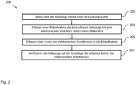
Weitere Ausführungsbeispiele werden Bezug nehmend auf die beiliegenden Figuren näher erläutert. Es zeigen:
- Fig. 1
- ein schematisches Diagramm einer Inspektionsvorrichtung zum Verifizieren eines Chipkartenhalbzeugs mit einem elektronischen Schaltkreis gemäß einer Ausführungsform; und
- Fig. 2
- ein Diagramm mit den Schritten eines Verfahrens zum Verifizieren eines Chipkartenhalbzeugs gemäß einer Ausführungsform.
- Fig. 1
- a schematic diagram of an inspection device for verifying a chip card semi-finished with an electronic circuit according to one embodiment; and
- Fig. 2
- a diagram showing the steps of a method for verifying a chip card semi-finished product according to an embodiment.
Bei der in
Die in
Die Inspektionsvorrichtung 100 umfasst ferner eine Bildkamera 107, welche ausgebildet ist, eine Bildaufnahme des beleuchteten Halbzeugs 101 mit dem elektronischen Schaltkreis 104 zu erfassen. Hierzu kann das Halbzeug 101 zwischen der Beleuchtungsquelle 105 und der Bildkamera 107 angeordnet sein. In dem Fall einer Beleuchtungsquelle 105 in Form einer Punktlichtquelle kann die Punktlichtquelle relativ zu der Bildkamera 107 von dem elektronischen Schaltkreis 104 verdeckt werden. Ebenso können die Beleuchtungsquelle 105 und die Bildkamera 107 auf derselben Seite des Halbzeugs 101 angeordnet sein. Bei der Bildkamera 107 kann es sich insbesondere um eine Digitalbildkamera handeln. Gemäß einer Ausführungsform ist die Bildkamera 107 ausgebildet, die Bildaufnahme des beleuchteten Halbzeugs 101 mit dem elektronischen Schaltkreis 104 im UV-Licht zu erfassen.The
Die Inspektionsvorrichtung 100 umfasst ferner einen Prozessor 109, welcher ausgebildet ist, in der Bildaufnahme eine Kontur des elektronischen Schaltkreises 104 zu erfassen und auf der Grundlage der erfassten Kontur des elektronischen Schaltkreises 104 das Halbzeug 101 zu verifizieren. Gemäß einer Ausführungsform ist der Prozessor 109 ausgebildet, die Kontur des elektronischen Schaltkreises 104, insbesondere durch Kantenerkennung oder Mustererkennung, zu erfassen.The
Gemäß einer Ausführungsform kann ein Verifizieren des Halbzeugs 101 auf der Grundlage der erfassten Kontur des elektronischen Schaltkreises 104 durch den Prozessor 109 beispielsweise eine Bewertung durch den Prozessor 109 umfassen, ob das Halbzeug 101 fehlerfrei ist oder möglicherweise einen Fehler aufweist und daher näher untersucht und/oder aussortiert werden sollte.According to one embodiment, verifying the
Der Prozessor 109 kann Teil eines Computers (nicht dargestellt) sein, der ein Display zur Anzeige der von der Bildkamera 107 erfassten und vom Prozessor 109 gegebenenfalls weiter verarbeiteten Bildaufnahme umfassen kann.The
Gemäß einer Ausführungsform kann der Prozessor 109 ausgebildet sein, auf der Grundlage der erfassten Kontur des elektronischen Schaltkreises 104 zu bestimmen, ob das Halbzeug 101 überhaupt mit einem elektronischen Schaltkreis bestückt ist, d.h. ob überhaupt ein elektronischer Schaltkreis in der Bildaufnahme vorhanden ist (Chip vorhanden ja/nein?) und/oder ob die Anordnung/Lage und oder die Orientierung des elektronischen Schaltkreises 104 relativ zu dem Halbzeug 101 stimmt.According to one embodiment, the
Gemäß einer Ausführungsform ist der Prozessor 109 ausgebildet, die Größe der von der Kontur des elektronischen Schaltkreises begrenzten Fläche in der Bildaufnahme zu bestimmen und das Halbzeug 101 auf der Grundlage der Größe der von der Kontur begrenzten Fläche zu verifizieren.According to one embodiment, the
Gemäß einer Ausführungsform kann der Prozessor 109 ausgebildet sein, auf der Grundlage der Größe der von der Kontur begrenzten Fläche zu bestimmen, ob der elektronische Schaltkreis 104 die korrekten Abmessungen aufweist (Chip korrekte Abmessungen / Chip gebrochen?). Beispielsweise könnte der Prozessor 109 ein Halbzeug 101 verwerfen, falls die Größe der von der Kontur des elektronischen Schaltkreises 104 begrenzten Fläche kleiner als ein erster Flächenschwellenwert ist, da ein Bruch des elektronischen Schaltkreises 104 eine Ursache für die kleinere Fläche der Kontur des elektronischen Schaltkreises 104 sein könnte. Ebenso könnte der Prozessor 109 ausgebildet sein, ein Halbzeug 101 zu verwerfen, falls die Größe der von der Kontur des elektronischen Schaltkreises 104 begrenzten Fläche größer als ein zweiter Flächenschwellenwert ist, der größer als der erste Flächenschwellenwert ist, da dies dafür sprechen könnte, dass versehentlich das Halbzeug 101 mit mehr als einem elektronischen Schaltkreis 104 bestückt worden ist.According to one embodiment, the
Gemäß einer Ausführungsform ist der Prozessor 109 ausgebildet, in der Bildaufnahme innerhalb der Kontur des elektronischen Schaltkreises 104 die Anzahl der zusammenhängenden Pixel zu bestimmen, deren Lichtintensität kleiner als ein erster Intensitätsschwellenwert ist, um die Größe der von der Kontur des elektronischen Schaltkreises 104 begrenzten Fläche zu bestimmen. Ein beispielhafter erster Intensitätsschwellenwert kann 1%, 5% oder 10% der in der Bildaufnahme auftretenden Maximalintensität betragen.According to one embodiment, the
Gemäß einer Ausführungsform ist die Bildkamera 107 ausgebildet, die Bildaufnahme zu überbelichten, um in der Bildaufnahme Bereiche außerhalb der Kontur des elektronischen Schaltkreises 104 auszublenden. Alternativ oder zusätzlich ist die Beleuchtungsquelle 105 ausgebildet ist, das Halbzeug 101 mit Licht einer vorbestimmten Intensität zu überbelichten, um in der Bildaufnahme Bereiche außerhalb der Kontur des elektronischen Schaltkreises 104 auszublenden.According to one embodiment, the
Mittels einer solchen Überbelichtung durch eine geeignete Ansteuerung der Beleuchtungsquelle 105 (z.B. über die Intensität der Beleuchtungsquelle 105) und/oder der Bildkamera 107 (z.B. über die Belichtungszeit) durch den Prozessor 109 kann die Analyse und Verarbeitung der Bildaufnahme durch den Prozessor 109 effizienter durchgeführt werden. Beispielsweise führt bei der in
Gemäß einer Ausführungsform umfasst der Schritt 205 des Erfassens der Kontur des elektronischen Schaltkreises 104 das Bestimmen der Größe der von der Kontur des elektronischen Schaltkreises 104 begrenzten Fläche und der Schritt 207 des Verifizierens des Halbzeugs 101 das Verifizieren des Halbzeugs 101 auf der Grundlage der Größe der von der Kontur begrenzten Fläche.According to an embodiment, the
Gemäß einer Ausführungsform wird die Größe der von der Kontur des elektronischen Schaltkreises 104 begrenzten Fläche bestimmt, indem in der Bildaufnahme innerhalb der Kontur des elektronischen Schaltkreises 104 die Anzahl der zusammenhängenden Pixel bestimmt wird, deren Lichtintensität kleiner als ein erster Intensitätsschwellenwert ist. Gemäß einer Ausführungsform kann die Kontur des elektronischen Schaltkreises 104, insbesondere durch Kantenerkennung oder Mustererkennung, erfasst werden.According to one embodiment, the size of the area bounded by the contour of the
Gemäß einer Ausführungsform kann die Bildaufnahme durch die Bildkamera 107 überbelichtet werden, um in der Bildaufnahme Bereiche außerhalb der Kontur des elektronischen Schaltkreises auszublenden.According to one embodiment, the image capture by the
Gemäß einer Ausführungsform kann das Halbzeug 101 mittels der Beleuchtungsquelle 105 mit Licht einer vorbestimmten Intensität überbelichtet werden, um in der Bildaufnahme Bereiche außerhalb der Kontur des elektronischen Schaltkreises 104 auszublenden.According to one embodiment, the
Gemäß einer Ausführungsform umfasst der Schritt 201 des Beleuchtens des Halbzeugs 101 mittels der Beleuchtungsquelle 105 das Beleuchten des Halbzeugs 101 mit UV-Licht und/oder der Schritt 203 des Erfassens der Bildaufnahme des beleuchteten Halbzeugs 101 mit dem elektronischen Schaltkreis 104 mittels der Bildkamera 107 umfasst das Erfassen der Bildaufnahme im UV-Licht.According to one embodiment, the
- 100100
- Inspektionsvorrichtunginspection device
- 101101
- HalbzeugWorkpiece
- 102102
- Trägerfoliesupport film
- 103103
- Ausgleichsfoliebalance sheet
- 104104
- elektronischer Schaltkreiselectronic circuit
- 105105
- Beleuchtungsquellelighting source
- 107107
- Bildkameracamera
- 109109
- Prozessorprocessor
- 200200
- Verfahren zum Verifizieren eines Halbzeugs mit einem elektronischen SchaltkreisMethod for verifying a semifinished product with an electronic circuit
- 201201
- Beleuchten des HalbzeugsIlluminate the semi-finished product
- 203203
- Erfassen einer Bildaufnahme des HalbzeugsCapture an image of the semifinished product
- 205205
- Erfassen einer Kontur des elektronischen SchaltkreisesDetecting a contour of the electronic circuit
- 207207
- Verifizieren des Halbzeugs anhand der KonturVerifying the semifinished product based on the contour
Claims (15)
Applications Claiming Priority (1)
| Application Number | Priority Date | Filing Date | Title |
|---|---|---|---|
| DE102015122726.6A DE102015122726A1 (en) | 2015-12-23 | 2015-12-23 | Inspection device and method for verifying a chip card semi-finished product |
Publications (2)
| Publication Number | Publication Date |
|---|---|
| EP3184997A1 true EP3184997A1 (en) | 2017-06-28 |
| EP3184997B1 EP3184997B1 (en) | 2020-09-16 |
Family
ID=57570775
Family Applications (1)
| Application Number | Title | Priority Date | Filing Date |
|---|---|---|---|
| EP16205209.6A Active EP3184997B1 (en) | 2015-12-23 | 2016-12-20 | Inspection device and method for verifying a semifinished chip card product |
Country Status (2)
| Country | Link |
|---|---|
| EP (1) | EP3184997B1 (en) |
| DE (1) | DE102015122726A1 (en) |
Families Citing this family (1)
| Publication number | Priority date | Publication date | Assignee | Title |
|---|---|---|---|---|
| CN105513991B (en) * | 2015-12-14 | 2018-07-20 | 重庆远创光电科技有限公司 | The control method of chip image is obtained using chip motion camera sleep mode |
Citations (6)
| Publication number | Priority date | Publication date | Assignee | Title |
|---|---|---|---|---|
| US4390955A (en) * | 1978-09-28 | 1983-06-28 | Tokyo Shibaura Denki Kabushiki Kaisha | Position detecting system |
| JPH0587546A (en) * | 1990-04-28 | 1993-04-06 | Seiwa Sangyo Kk | Method and device for inspecting appearance |
| WO2011003518A1 (en) | 2009-07-09 | 2011-01-13 | Bundesdruckerei Gmbh | Method and apparatus for producing an inlay for a film composite, and film composite with inlay |
| DE102011001722A1 (en) | 2011-04-01 | 2012-10-04 | Bundesdruckerei Gmbh | Semi-finished product for the production of a chip card module, method for producing the semifinished product and method for producing a chip card |
| EP2583826A1 (en) * | 2011-10-19 | 2013-04-24 | Giesecke & Devrient GmbH | Production of an inlay with integrated control circuit |
| DE102012223472A1 (en) * | 2012-12-17 | 2014-06-18 | Bundesdruckerei Gmbh | Method and device for producing a value and / or security document with an antenna structure |
Family Cites Families (2)
| Publication number | Priority date | Publication date | Assignee | Title |
|---|---|---|---|---|
| WO2005069082A1 (en) * | 2003-12-19 | 2005-07-28 | International Business Machines Corporation | Differential critical dimension and overlay metrology apparatus and measurement method |
| US7561022B2 (en) * | 2004-01-13 | 2009-07-14 | George Schmitt & Company, Inc. | System and method for validating radio frequency identification tags |
-
2015
- 2015-12-23 DE DE102015122726.6A patent/DE102015122726A1/en not_active Withdrawn
-
2016
- 2016-12-20 EP EP16205209.6A patent/EP3184997B1/en active Active
Patent Citations (6)
| Publication number | Priority date | Publication date | Assignee | Title |
|---|---|---|---|---|
| US4390955A (en) * | 1978-09-28 | 1983-06-28 | Tokyo Shibaura Denki Kabushiki Kaisha | Position detecting system |
| JPH0587546A (en) * | 1990-04-28 | 1993-04-06 | Seiwa Sangyo Kk | Method and device for inspecting appearance |
| WO2011003518A1 (en) | 2009-07-09 | 2011-01-13 | Bundesdruckerei Gmbh | Method and apparatus for producing an inlay for a film composite, and film composite with inlay |
| DE102011001722A1 (en) | 2011-04-01 | 2012-10-04 | Bundesdruckerei Gmbh | Semi-finished product for the production of a chip card module, method for producing the semifinished product and method for producing a chip card |
| EP2583826A1 (en) * | 2011-10-19 | 2013-04-24 | Giesecke & Devrient GmbH | Production of an inlay with integrated control circuit |
| DE102012223472A1 (en) * | 2012-12-17 | 2014-06-18 | Bundesdruckerei Gmbh | Method and device for producing a value and / or security document with an antenna structure |
Also Published As
| Publication number | Publication date |
|---|---|
| EP3184997B1 (en) | 2020-09-16 |
| DE102015122726A1 (en) | 2017-06-29 |
Similar Documents
| Publication | Publication Date | Title |
|---|---|---|
| EP2956915B1 (en) | Method for authenticating an identification document | |
| EP2736026B1 (en) | Device for reading out a magnetic strip and/or chip card with a camera for detecting inserted skimming modules | |
| EP2414240B1 (en) | Transport bin identification | |
| DE102015108330A1 (en) | Electronic access control procedure | |
| DE202008007564U1 (en) | Device for personalizing a chip card | |
| EP2932439B1 (en) | Method and device for producing a value document and/or a security document having an antenna structure | |
| EP3184997B1 (en) | Inspection device and method for verifying a semifinished chip card product | |
| EP3184999B1 (en) | Inspection device and method for verifying an adhesive connection | |
| EP3357043B1 (en) | Document and process for verifying a document | |
| EP3024666B1 (en) | Method for verifying the authenticity of a document | |
| DE102015122729B4 (en) | Inspection device and method for verifying a chip card semi-finished product | |
| EP3184996B1 (en) | Inspection device and method for verifying a semifinished chip card product | |
| EP2394250B1 (en) | Method and device for verifying document using a wavelet transformation | |
| EP2899699B1 (en) | Method for assessing the authenticity of an identification document | |
| DE102011087637A1 (en) | Identification document with a machine-readable zone and document reader | |
| DE202008011224U1 (en) | Testing device for electronic components | |
| DE102005040852A1 (en) | Scanner for scanning transponder-containing documents e.g. passports has optical reflecting metal layer that is provided on mirror and is divided into mirror segments | |
| WO2017129460A1 (en) | Authentication device, authentication document, and method for authenticating a person | |
| DE102013002375A1 (en) | Method for calibrating camera of motor car in parking aid, involves detecting reference object in image using camera, and processing image, in order to recognize parameter stored in reference pattern of camera | |
| DE102020120962B4 (en) | Recognition method and recognition system for clearly recognizing an object | |
| EP3499865B1 (en) | Device and method for measuring image data | |
| EP3338254B1 (en) | Authenticating device for a document | |
| EP2926323B1 (en) | Method and device for testing a laser marking produced in accordance with an angle on a document surface | |
| EP4320603A1 (en) | Device and method for checking a marking of a product | |
| DE102016101607A1 (en) | Authentication device for authenticating a person |
Legal Events
| Date | Code | Title | Description |
|---|---|---|---|
| PUAI | Public reference made under article 153(3) epc to a published international application that has entered the european phase |
Free format text: ORIGINAL CODE: 0009012 |
|
| STAA | Information on the status of an ep patent application or granted ep patent |
Free format text: STATUS: THE APPLICATION HAS BEEN PUBLISHED |
|
| AK | Designated contracting states |
Kind code of ref document: A1 Designated state(s): AL AT BE BG CH CY CZ DE DK EE ES FI FR GB GR HR HU IE IS IT LI LT LU LV MC MK MT NL NO PL PT RO RS SE SI SK SM TR |
|
| AX | Request for extension of the european patent |
Extension state: BA ME |
|
| STAA | Information on the status of an ep patent application or granted ep patent |
Free format text: STATUS: REQUEST FOR EXAMINATION WAS MADE |
|
| 17P | Request for examination filed |
Effective date: 20171212 |
|
| RBV | Designated contracting states (corrected) |
Designated state(s): AL AT BE BG CH CY CZ DE DK EE ES FI FR GB GR HR HU IE IS IT LI LT LU LV MC MK MT NL NO PL PT RO RS SE SI SK SM TR |
|
| STAA | Information on the status of an ep patent application or granted ep patent |
Free format text: STATUS: EXAMINATION IS IN PROGRESS |
|
| 17Q | First examination report despatched |
Effective date: 20180717 |
|
| GRAP | Despatch of communication of intention to grant a patent |
Free format text: ORIGINAL CODE: EPIDOSNIGR1 |
|
| STAA | Information on the status of an ep patent application or granted ep patent |
Free format text: STATUS: GRANT OF PATENT IS INTENDED |
|
| INTG | Intention to grant announced |
Effective date: 20200626 |
|
| GRAS | Grant fee paid |
Free format text: ORIGINAL CODE: EPIDOSNIGR3 |
|
| GRAA | (expected) grant |
Free format text: ORIGINAL CODE: 0009210 |
|
| STAA | Information on the status of an ep patent application or granted ep patent |
Free format text: STATUS: THE PATENT HAS BEEN GRANTED |
|
| AK | Designated contracting states |
Kind code of ref document: B1 Designated state(s): AL AT BE BG CH CY CZ DE DK EE ES FI FR GB GR HR HU IE IS IT LI LT LU LV MC MK MT NL NO PL PT RO RS SE SI SK SM TR |
|
| REG | Reference to a national code |
Ref country code: GB Ref legal event code: FG4D Free format text: NOT ENGLISH |
|
| REG | Reference to a national code |
Ref country code: CH Ref legal event code: EP |
|
| REG | Reference to a national code |
Ref country code: DE Ref legal event code: R096 Ref document number: 502016011173 Country of ref document: DE |
|
| REG | Reference to a national code |
Ref country code: IE Ref legal event code: FG4D Free format text: LANGUAGE OF EP DOCUMENT: GERMAN |
|
| REG | Reference to a national code |
Ref country code: AT Ref legal event code: REF Ref document number: 1314603 Country of ref document: AT Kind code of ref document: T Effective date: 20201015 |
|
| PG25 | Lapsed in a contracting state [announced via postgrant information from national office to epo] |
Ref country code: SE Free format text: LAPSE BECAUSE OF FAILURE TO SUBMIT A TRANSLATION OF THE DESCRIPTION OR TO PAY THE FEE WITHIN THE PRESCRIBED TIME-LIMIT Effective date: 20200916 Ref country code: HR Free format text: LAPSE BECAUSE OF FAILURE TO SUBMIT A TRANSLATION OF THE DESCRIPTION OR TO PAY THE FEE WITHIN THE PRESCRIBED TIME-LIMIT Effective date: 20200916 Ref country code: GR Free format text: LAPSE BECAUSE OF FAILURE TO SUBMIT A TRANSLATION OF THE DESCRIPTION OR TO PAY THE FEE WITHIN THE PRESCRIBED TIME-LIMIT Effective date: 20201217 Ref country code: NO Free format text: LAPSE BECAUSE OF FAILURE TO SUBMIT A TRANSLATION OF THE DESCRIPTION OR TO PAY THE FEE WITHIN THE PRESCRIBED TIME-LIMIT Effective date: 20201216 Ref country code: BG Free format text: LAPSE BECAUSE OF FAILURE TO SUBMIT A TRANSLATION OF THE DESCRIPTION OR TO PAY THE FEE WITHIN THE PRESCRIBED TIME-LIMIT Effective date: 20201216 Ref country code: FI Free format text: LAPSE BECAUSE OF FAILURE TO SUBMIT A TRANSLATION OF THE DESCRIPTION OR TO PAY THE FEE WITHIN THE PRESCRIBED TIME-LIMIT Effective date: 20200916 |
|
| REG | Reference to a national code |
Ref country code: NL Ref legal event code: MP Effective date: 20200916 |
|
| PG25 | Lapsed in a contracting state [announced via postgrant information from national office to epo] |
Ref country code: RS Free format text: LAPSE BECAUSE OF FAILURE TO SUBMIT A TRANSLATION OF THE DESCRIPTION OR TO PAY THE FEE WITHIN THE PRESCRIBED TIME-LIMIT Effective date: 20200916 Ref country code: LV Free format text: LAPSE BECAUSE OF FAILURE TO SUBMIT A TRANSLATION OF THE DESCRIPTION OR TO PAY THE FEE WITHIN THE PRESCRIBED TIME-LIMIT Effective date: 20200916 |
|
| REG | Reference to a national code |
Ref country code: LT Ref legal event code: MG4D |
|
| PG25 | Lapsed in a contracting state [announced via postgrant information from national office to epo] |
Ref country code: LT Free format text: LAPSE BECAUSE OF FAILURE TO SUBMIT A TRANSLATION OF THE DESCRIPTION OR TO PAY THE FEE WITHIN THE PRESCRIBED TIME-LIMIT Effective date: 20200916 Ref country code: PT Free format text: LAPSE BECAUSE OF FAILURE TO SUBMIT A TRANSLATION OF THE DESCRIPTION OR TO PAY THE FEE WITHIN THE PRESCRIBED TIME-LIMIT Effective date: 20210118 Ref country code: SM Free format text: LAPSE BECAUSE OF FAILURE TO SUBMIT A TRANSLATION OF THE DESCRIPTION OR TO PAY THE FEE WITHIN THE PRESCRIBED TIME-LIMIT Effective date: 20200916 Ref country code: RO Free format text: LAPSE BECAUSE OF FAILURE TO SUBMIT A TRANSLATION OF THE DESCRIPTION OR TO PAY THE FEE WITHIN THE PRESCRIBED TIME-LIMIT Effective date: 20200916 Ref country code: CZ Free format text: LAPSE BECAUSE OF FAILURE TO SUBMIT A TRANSLATION OF THE DESCRIPTION OR TO PAY THE FEE WITHIN THE PRESCRIBED TIME-LIMIT Effective date: 20200916 Ref country code: EE Free format text: LAPSE BECAUSE OF FAILURE TO SUBMIT A TRANSLATION OF THE DESCRIPTION OR TO PAY THE FEE WITHIN THE PRESCRIBED TIME-LIMIT Effective date: 20200916 |
|
| PG25 | Lapsed in a contracting state [announced via postgrant information from national office to epo] |
Ref country code: AL Free format text: LAPSE BECAUSE OF FAILURE TO SUBMIT A TRANSLATION OF THE DESCRIPTION OR TO PAY THE FEE WITHIN THE PRESCRIBED TIME-LIMIT Effective date: 20200916 Ref country code: ES Free format text: LAPSE BECAUSE OF FAILURE TO SUBMIT A TRANSLATION OF THE DESCRIPTION OR TO PAY THE FEE WITHIN THE PRESCRIBED TIME-LIMIT Effective date: 20200916 Ref country code: IS Free format text: LAPSE BECAUSE OF FAILURE TO SUBMIT A TRANSLATION OF THE DESCRIPTION OR TO PAY THE FEE WITHIN THE PRESCRIBED TIME-LIMIT Effective date: 20210116 Ref country code: PL Free format text: LAPSE BECAUSE OF FAILURE TO SUBMIT A TRANSLATION OF THE DESCRIPTION OR TO PAY THE FEE WITHIN THE PRESCRIBED TIME-LIMIT Effective date: 20200916 |
|
| REG | Reference to a national code |
Ref country code: DE Ref legal event code: R097 Ref document number: 502016011173 Country of ref document: DE |
|
| PG25 | Lapsed in a contracting state [announced via postgrant information from national office to epo] |
Ref country code: SK Free format text: LAPSE BECAUSE OF FAILURE TO SUBMIT A TRANSLATION OF THE DESCRIPTION OR TO PAY THE FEE WITHIN THE PRESCRIBED TIME-LIMIT Effective date: 20200916 |
|
| PLBE | No opposition filed within time limit |
Free format text: ORIGINAL CODE: 0009261 |
|
| STAA | Information on the status of an ep patent application or granted ep patent |
Free format text: STATUS: NO OPPOSITION FILED WITHIN TIME LIMIT |
|
| REG | Reference to a national code |
Ref country code: CH Ref legal event code: PL |
|
| 26N | No opposition filed |
Effective date: 20210617 |
|
| PG25 | Lapsed in a contracting state [announced via postgrant information from national office to epo] |
Ref country code: MC Free format text: LAPSE BECAUSE OF FAILURE TO SUBMIT A TRANSLATION OF THE DESCRIPTION OR TO PAY THE FEE WITHIN THE PRESCRIBED TIME-LIMIT Effective date: 20200916 Ref country code: DK Free format text: LAPSE BECAUSE OF FAILURE TO SUBMIT A TRANSLATION OF THE DESCRIPTION OR TO PAY THE FEE WITHIN THE PRESCRIBED TIME-LIMIT Effective date: 20200916 Ref country code: SI Free format text: LAPSE BECAUSE OF FAILURE TO SUBMIT A TRANSLATION OF THE DESCRIPTION OR TO PAY THE FEE WITHIN THE PRESCRIBED TIME-LIMIT Effective date: 20200916 |
|
| REG | Reference to a national code |
Ref country code: BE Ref legal event code: MM Effective date: 20201231 |
|
| PG25 | Lapsed in a contracting state [announced via postgrant information from national office to epo] |
Ref country code: IT Free format text: LAPSE BECAUSE OF FAILURE TO SUBMIT A TRANSLATION OF THE DESCRIPTION OR TO PAY THE FEE WITHIN THE PRESCRIBED TIME-LIMIT Effective date: 20200916 Ref country code: IE Free format text: LAPSE BECAUSE OF NON-PAYMENT OF DUE FEES Effective date: 20201220 Ref country code: LU Free format text: LAPSE BECAUSE OF NON-PAYMENT OF DUE FEES Effective date: 20201220 |
|
| PG25 | Lapsed in a contracting state [announced via postgrant information from national office to epo] |
Ref country code: LI Free format text: LAPSE BECAUSE OF NON-PAYMENT OF DUE FEES Effective date: 20201231 Ref country code: CH Free format text: LAPSE BECAUSE OF NON-PAYMENT OF DUE FEES Effective date: 20201231 |
|
| PG25 | Lapsed in a contracting state [announced via postgrant information from national office to epo] |
Ref country code: TR Free format text: LAPSE BECAUSE OF FAILURE TO SUBMIT A TRANSLATION OF THE DESCRIPTION OR TO PAY THE FEE WITHIN THE PRESCRIBED TIME-LIMIT Effective date: 20200916 Ref country code: MT Free format text: LAPSE BECAUSE OF FAILURE TO SUBMIT A TRANSLATION OF THE DESCRIPTION OR TO PAY THE FEE WITHIN THE PRESCRIBED TIME-LIMIT Effective date: 20200916 Ref country code: CY Free format text: LAPSE BECAUSE OF FAILURE TO SUBMIT A TRANSLATION OF THE DESCRIPTION OR TO PAY THE FEE WITHIN THE PRESCRIBED TIME-LIMIT Effective date: 20200916 |
|
| PG25 | Lapsed in a contracting state [announced via postgrant information from national office to epo] |
Ref country code: MK Free format text: LAPSE BECAUSE OF FAILURE TO SUBMIT A TRANSLATION OF THE DESCRIPTION OR TO PAY THE FEE WITHIN THE PRESCRIBED TIME-LIMIT Effective date: 20200916 |
|
| PG25 | Lapsed in a contracting state [announced via postgrant information from national office to epo] |
Ref country code: BE Free format text: LAPSE BECAUSE OF NON-PAYMENT OF DUE FEES Effective date: 20201231 |
|
| REG | Reference to a national code |
Ref country code: AT Ref legal event code: MM01 Ref document number: 1314603 Country of ref document: AT Kind code of ref document: T Effective date: 20211220 |
|
| PG25 | Lapsed in a contracting state [announced via postgrant information from national office to epo] |
Ref country code: AT Free format text: LAPSE BECAUSE OF NON-PAYMENT OF DUE FEES Effective date: 20211220 |
|
| PG25 | Lapsed in a contracting state [announced via postgrant information from national office to epo] |
Ref country code: NL Free format text: LAPSE BECAUSE OF NON-PAYMENT OF DUE FEES Effective date: 20200923 |
|
| P01 | Opt-out of the competence of the unified patent court (upc) registered |
Effective date: 20230526 |
|
| PGFP | Annual fee paid to national office [announced via postgrant information from national office to epo] |
Ref country code: GB Payment date: 20231220 Year of fee payment: 8 |
|
| PGFP | Annual fee paid to national office [announced via postgrant information from national office to epo] |
Ref country code: FR Payment date: 20231219 Year of fee payment: 8 Ref country code: DE Payment date: 20231214 Year of fee payment: 8 |