EP3183091B1 - Sapphire collector for reducing mechanical damage during die level laser lift-off - Google Patents
Sapphire collector for reducing mechanical damage during die level laser lift-off Download PDFInfo
- Publication number
- EP3183091B1 EP3183091B1 EP15760269.9A EP15760269A EP3183091B1 EP 3183091 B1 EP3183091 B1 EP 3183091B1 EP 15760269 A EP15760269 A EP 15760269A EP 3183091 B1 EP3183091 B1 EP 3183091B1
- Authority
- EP
- European Patent Office
- Prior art keywords
- cavity
- opening
- chips
- collection system
- chip
- Prior art date
- Legal status (The legal status is an assumption and is not a legal conclusion. Google has not performed a legal analysis and makes no representation as to the accuracy of the status listed.)
- Active
Links
Images

Classifications
-
- B—PERFORMING OPERATIONS; TRANSPORTING
- B23—MACHINE TOOLS; METAL-WORKING NOT OTHERWISE PROVIDED FOR
- B23K—SOLDERING OR UNSOLDERING; WELDING; CLADDING OR PLATING BY SOLDERING OR WELDING; CUTTING BY APPLYING HEAT LOCALLY, e.g. FLAME CUTTING; WORKING BY LASER BEAM
- B23K26/00—Working by laser beam, e.g. welding, cutting or boring
- B23K26/14—Working by laser beam, e.g. welding, cutting or boring using a fluid stream, e.g. a jet of gas, in conjunction with the laser beam; Nozzles therefor
- B23K26/142—Working by laser beam, e.g. welding, cutting or boring using a fluid stream, e.g. a jet of gas, in conjunction with the laser beam; Nozzles therefor for the removal of by-products
-
- B—PERFORMING OPERATIONS; TRANSPORTING
- B23—MACHINE TOOLS; METAL-WORKING NOT OTHERWISE PROVIDED FOR
- B23K—SOLDERING OR UNSOLDERING; WELDING; CLADDING OR PLATING BY SOLDERING OR WELDING; CUTTING BY APPLYING HEAT LOCALLY, e.g. FLAME CUTTING; WORKING BY LASER BEAM
- B23K26/00—Working by laser beam, e.g. welding, cutting or boring
- B23K26/0006—Working by laser beam, e.g. welding, cutting or boring taking account of the properties of the material involved
-
- B—PERFORMING OPERATIONS; TRANSPORTING
- B23—MACHINE TOOLS; METAL-WORKING NOT OTHERWISE PROVIDED FOR
- B23K—SOLDERING OR UNSOLDERING; WELDING; CLADDING OR PLATING BY SOLDERING OR WELDING; CUTTING BY APPLYING HEAT LOCALLY, e.g. FLAME CUTTING; WORKING BY LASER BEAM
- B23K26/00—Working by laser beam, e.g. welding, cutting or boring
- B23K26/02—Positioning or observing the workpiece, e.g. with respect to the point of impact; Aligning, aiming or focusing the laser beam
- B23K26/06—Shaping the laser beam, e.g. by masks or multi-focusing
- B23K26/062—Shaping the laser beam, e.g. by masks or multi-focusing by direct control of the laser beam
- B23K26/0622—Shaping the laser beam, e.g. by masks or multi-focusing by direct control of the laser beam by shaping pulses
-
- B—PERFORMING OPERATIONS; TRANSPORTING
- B23—MACHINE TOOLS; METAL-WORKING NOT OTHERWISE PROVIDED FOR
- B23K—SOLDERING OR UNSOLDERING; WELDING; CLADDING OR PLATING BY SOLDERING OR WELDING; CUTTING BY APPLYING HEAT LOCALLY, e.g. FLAME CUTTING; WORKING BY LASER BEAM
- B23K26/00—Working by laser beam, e.g. welding, cutting or boring
- B23K26/352—Working by laser beam, e.g. welding, cutting or boring for surface treatment
- B23K26/356—Working by laser beam, e.g. welding, cutting or boring for surface treatment by shock processing
-
- H—ELECTRICITY
- H10—SEMICONDUCTOR DEVICES; ELECTRIC SOLID-STATE DEVICES NOT OTHERWISE PROVIDED FOR
- H10H—INORGANIC LIGHT-EMITTING SEMICONDUCTOR DEVICES HAVING POTENTIAL BARRIERS
- H10H20/00—Individual inorganic light-emitting semiconductor devices having potential barriers, e.g. light-emitting diodes [LED]
- H10H20/01—Manufacture or treatment
- H10H20/011—Manufacture or treatment of bodies, e.g. forming semiconductor layers
- H10H20/018—Bonding of wafers
-
- B—PERFORMING OPERATIONS; TRANSPORTING
- B23—MACHINE TOOLS; METAL-WORKING NOT OTHERWISE PROVIDED FOR
- B23K—SOLDERING OR UNSOLDERING; WELDING; CLADDING OR PLATING BY SOLDERING OR WELDING; CUTTING BY APPLYING HEAT LOCALLY, e.g. FLAME CUTTING; WORKING BY LASER BEAM
- B23K2101/00—Articles made by soldering, welding or cutting
- B23K2101/36—Electric or electronic devices
- B23K2101/40—Semiconductor devices
-
- B—PERFORMING OPERATIONS; TRANSPORTING
- B23—MACHINE TOOLS; METAL-WORKING NOT OTHERWISE PROVIDED FOR
- B23K—SOLDERING OR UNSOLDERING; WELDING; CLADDING OR PLATING BY SOLDERING OR WELDING; CUTTING BY APPLYING HEAT LOCALLY, e.g. FLAME CUTTING; WORKING BY LASER BEAM
- B23K2101/00—Articles made by soldering, welding or cutting
- B23K2101/36—Electric or electronic devices
- B23K2101/42—Printed circuits
-
- B—PERFORMING OPERATIONS; TRANSPORTING
- B23—MACHINE TOOLS; METAL-WORKING NOT OTHERWISE PROVIDED FOR
- B23K—SOLDERING OR UNSOLDERING; WELDING; CLADDING OR PLATING BY SOLDERING OR WELDING; CUTTING BY APPLYING HEAT LOCALLY, e.g. FLAME CUTTING; WORKING BY LASER BEAM
- B23K2103/00—Materials to be soldered, welded or cut
- B23K2103/16—Composite materials
- B23K2103/166—Multilayered materials
- B23K2103/172—Multilayered materials wherein at least one of the layers is non-metallic
-
- B—PERFORMING OPERATIONS; TRANSPORTING
- B23—MACHINE TOOLS; METAL-WORKING NOT OTHERWISE PROVIDED FOR
- B23K—SOLDERING OR UNSOLDERING; WELDING; CLADDING OR PLATING BY SOLDERING OR WELDING; CUTTING BY APPLYING HEAT LOCALLY, e.g. FLAME CUTTING; WORKING BY LASER BEAM
- B23K2103/00—Materials to be soldered, welded or cut
- B23K2103/50—Inorganic materials other than metals or composite materials
Definitions
- a barrier 280 may be placed around the pickup opening 222, forming a trench wherein the chips 170 are contained. Means may be provided for periodically removing the captured chips 170 from the trench formed by the barrier 280.
- the submount 150 or the SC 220 is moved quickly to place each next semiconductor 160 with chip 170 beneath the opening 222.
- the submount 150 travels at a varying velocity Vs due to acceleration and deceleration of stage movement, and the laser is activated when the semiconductor 160 with chip 170 is staged beneath the opening 222.
- the resulting velocity of the chip upon liftoff will be equal to the vector sum of the staging velocity Vs and the velocity induced by the vacuum Vv, including the initial velocity due to the laser separation of the chip 170 from the semiconductor 160.
- this vector sum Vvs must point into the opening 222.
Landscapes
- Physics & Mathematics (AREA)
- Optics & Photonics (AREA)
- Engineering & Computer Science (AREA)
- Plasma & Fusion (AREA)
- Mechanical Engineering (AREA)
- Laser Beam Processing (AREA)
- Semiconductor Lasers (AREA)
- Led Devices (AREA)
- Dicing (AREA)
- Die Bonding (AREA)
Description
- This invention relates to the field of light emitting devices, and in particular to a system that reduces damage to the light emitting devices during laser lift-off of the sapphire substrate upon which the light emitting element is grown.
- Semiconductor devices, including semiconductor light emitting elements, are formed/grown on a substrate, sapphire wafer substrates being common. In the example of a light emitting element, a GaN nucleation layer may be formed on a sapphire substrate, followed by one or more n-type layers, one or more active layers, and one or more p-type layers. Metallic conductors may be formed through and upon the layers to provide coupling of the n-type and p-type layers to an external source of power to activate the active layer(s) of the light emitting element, via contact pads above the uppermost (p-type) layer.
- Because the metallic contact pads are generally opaque or reflective, the light emitting element is designed to emit lights from the surface opposite the contact pads and through the substrate. To improve light extraction efficiency, the substrate may be removed, exposing the semiconductor surface. The semiconductor surface may be processed to further enhance the light extraction efficiency. In some cases one or more contact pads may be placed on the light emitting side of the device.
- Laser lift-off is a process that is commonly used to remove the sapphire substrate from the light emitting element. A laser pulse is projected through the sapphire substrate and is absorbed by the semiconductor layer at the Sapphire-semiconductor interface, producing a localized explosive shockwave, due to the instant thermal decomposition of the semiconductor layer at the interface.
- If the laser lift-off (LLO) is performed at the wafer level, the wafer-size sapphire substrate is removed after the whole wafer has been processed. If, on the other hand, the laser lift-off is performed for each individual die, the dies are flip-chip mounted on a submount tile, with the sapphire facing upward. The laser is applied to each die, and the die-size sapphire chips pop up into a "Sapphire Collector", or "Confetti Catcher" immediately after the laser is incident on each die, leaving the semiconductor structure on the submount tile. The sub-mount tile is subsequently processed to create, for example, lens elements over each die, then sliced/diced to provide the individual light emitting devices.
- Between the time that the sapphire is removed and the dies are covered, the relatively fragile semiconductor surface is exposed, and susceptible to mechanical damage. During an example set of production runs, the yield lost to such mechanical damage has been measured to be about 0.236%.
- It would be advantageous to reduce the likelihood of mechanical damage to a light emitting element after laser lift-off.
- To better address this concern, in an embodiment of this invention, one or more features, both structural and parametric, are included in a Sapphire Collector (SC) for capturing the die-size sapphire chips that are removed from a semiconductor structure during die-level laser lift-off (LLO). These features are designed to increase the likelihood that each sapphire chip is securely captured by the Sapphire Collector immediately after it is released from the semiconductor structure. The Sapphire Collector includes a vacuum-enhance collector with a pickup element that lifts each released chip into the collector, and air pushers that direct the chips further into the collection tunnel leading to a discard bin.
- In embodiments of this invention, the features that enhance the likelihood of a released sapphire chip being securely captured by the Sapphire Collector include one or more of the following.
- To reduce the likelihood of the chip striking a top surface of the collector and bouncing back exiting the pickup element, an angled air pusher may be situated near the top of the collector to direct the chips away from the top surface and farther into the collection tunnel. At the same time, a complementary angled air pusher may be situated near the bottom of the collector to also direct the picked-up chips farther into the collection tunnel, and further direct any ricocheted chips away from the pickup element. To further enhance the efficiency of these air pushers, the air pushers may be shaped as air knives with high velocity, low volume output.
- The entry to the collection tunnel may be flared to maximize the collection cross-section area, and to reduce the likelihood of a chip ricocheting back toward the pickup area. A trench may be created around the interior of the pickup element, to prevent any chips that manage to slide out of the flared tunnel opening, or otherwise coming near to the pickup element from exiting the pickup element.
- The exterior surface of the collector facing the dies on the sub-mount may be chamfered, to reduce the likelihood of a 'wild chip' ricocheting repeatedly between the sub-mount and the lower surface of the collector. The pickup element, and the provided vacuum may also be designed to optimize the likelihood that a released chip will be forced to enter the collector.
- In an example embodiment of this invention, the yield loss due to mechanical damage after laser lift-off was reduced by an order of magnitude, from 0.236% to 0.023%.
- The invention is explained in further detail, and by way of example, with reference to the accompanying drawings wherein:
-
FIG. 1A illustrates an example prior art Sapphire Collector. -
FIGs. 1B and 1C illustrate examples of adverse travel of a sapphire chip in the prior art Sapphire Collector ofFIG. 1A . -
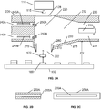
FIGs. 2A-2C illustrate an example embodiment of a Sapphire Collector that substantially reduces the likelihood of mechanical damage to the light emitting element after laser lift-off. -
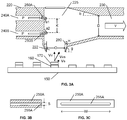
FIGs. 3A-3C illustrates example dimensions of the Sapphire Collector ofFIG. 2 . - Throughout the drawings, the same reference numerals indicate similar or corresponding features or functions. The drawings are included for illustrative purposes and are not intended to limit the scope of the invention.
- In the following description, for purposes of explanation rather than limitation, specific details are set forth such as the particular architecture, interfaces, techniques, etc., in order to provide a thorough understanding of the concepts of the invention. However, it will be apparent to those skilled in the art that the present invention may be practiced in other embodiments, which depart from these specific details. In like manner, the text of this description is directed to the example embodiments as illustrated in the Figures, and is not intended to limit the invention as defined by the appended claims beyond the limits expressly included in the claims. For purposes of simplicity and clarity, detailed descriptions of well-known devices, circuits, and methods are omitted so as not to obscure the description of the present invention with unnecessary detail.
-
FIG. 1A illustrates an example prior art Sapphire Collector (SC) 120. The SC 120 includes acollection cavity 125 that is open to twotunnels vacuum flows tunnels input pipes cavity 125 that providespressure flows pipes - A
laser element 110 provides apulsed laser beam 115 that enters SC 120 via agate 128. Thegate 128 is designed so as not to block thelaser beam 115, but to prevent the escape of anysapphire chips 170 after they enter thecavity 125. Thegate 128 may be, for example, a lens element, or simply a grate. - Below the
SC 120, a plurality oflight emitting elements 160 with attachedsapphire substrate chips 170 are mounted on asubmount 150. During laser lift-off, theSC 120 is situated over alight emitting element 160 with an attachedsapphire chip 170, either by movingSC 120 relative to thesubmount 150, or moving thesubmount 150 relative to theopening 122 to thecavity 125 ofSC 120. - With the
light emitting element 160 andchip 170 situated beneath theopening 122, thepulsed laser beam 115 is applied, causing thechip 170 to be explosively released from thelight emitting element 160. The upward force causes the releasedchip 170 to enter theopening 122 and the vacuum flows 135A and 13B causes it to travel toward thetunnels pipes chip 170 toward the tunnels 130. - Depending upon the initial liftoff trajectory direction and velocity of the
chip 170 relative to the vacuum 130 and pressurized air 145, thechip 170 may enter one of the vacuum tunnels 130 directly, or after a few ricochets. Ideally, even if thechip 170 ricochets around within thecavity 125, thechip 170 will eventually enter one of thetunnels vacuums pressurized air flows - The inventors have recorded the laser lift-off operation with respect to the
submount 150 and theopening 122 using a high speed camera, and have observed that somechips 170 exit theopening 122 and cause damage. - In some cases, the
chips 170 are hovering below theopening 122 and are eventually sucked back into thecavity 125, causing no adverse effects. In other cases, however, thechips 170 are traveling at a sufficient downward speed that the vacuum flows 135A, 135B andpressurized air flows opening 122 and strikes thesubmount 150, as illustrated inFIG. 1B . The likely cause of this downward travel is a ricochet of thechip 170 off the walls or top surface of thecavity 125. Most ricochetingchips 170 are likely to eventually be sucked into thetunnels chips 170 escape through theopening 122 and strike the sub-mount 150 with mountedlight emitting elements 160. - If the exiting
chip 170 strikes thesubmount 150 at a location where thelight emitting element 160 is situated without an attached sapphire chip 170 (i.e.elements 160 withchips 170 laser removed), even at a low speed, the fragile nature of the semiconductor surface will likely result in the ruin of theelement 160. -
FIG. 1C illustrates an observed failure mechanism wherein the exitingchip 170 ricochets repeatedly between thelower exterior surface 126 ofSC 120 and thesubmount 150, causing substantial damage, often tomultiple elements 160 on thesubmount 150. - As noted above, the yield loss due to mechanical damage after laser lift-off has been observed in one set of production runs to amount to 0.236%; and, as subsequently been determined, most (90%) of this lost yield is due to the damage that exiting
chips 170 inflict. It was also observed that a substantial majority of damage was produced due to the repeated ricochets illustrated inFIG. 1C . -
FIG. 2A illustrates an example embodiment of a Sapphire Collector (SC) 220 that substantially reduces the likelihood of mechanical damage to the light emitting element after laser lift-off. - Of particular note,
SC 220 includes asingle tunnel 230, with atubular portion 231 and a flaredportion 232. A narrow end of the flaredportion 232 is connected totubular portion 231 and a wide end is connected to acavity 225. Flaredportion 232 may be a conic section, such as a cone shape with a pointed end removed. Both the flaredportion 232 and thetubular portion 231 may have a circular cross section, or the shapes may be more complex. For example, flaredportion 232 may have a rectangular cross section at its wide end, where it opens into thecavity 225, and a circular cross section at its narrow end, where it couples to thetubular portion 231. In the alternative, the cross sections for the either the flaredportion 232 or thetubular portion 231 may have any suitable cross section e.g. square, triangular, elliptical. Likewisecavity 225 may have a rectangular cross section, a round cross section or any suitable cross section. The cross section ofcavity 225 may be the same along its entire height or it may differ. - The
tunnel 230 is held at negative pressure, resulting in a vacuum force orvacuum flow 235. Although thiswider tunnel 230 may require agreater vacuum force 235 than thenarrower tunnels FIG. 1 , features that reduce the loss of the created vacuum may be provided, as detailed further below. - A
laser element 110 provides apulsed laser beam 115 that entersSC 220 via agate 128. Thegate 128 is designed so as not to block thelaser beam 115, but to prevent the escape of anysapphire chips 170 after they enter thecavity 225. Thegate 128 may be, for example, a lens element, or simply a grate. - Below the
SC 220, a plurality oflight emitting elements 160 with attachedsapphire substrate chips 170 are mounted on asubmount 150. During laser lift-off, theSC 220 is situated over alight emitting element 160 with an attachedsapphire chip 170, either by movingSC 220 relative to thesubmount 150, or moving thesubmount 150 relative to theopening 222 to thecavity 225 ofSC 220. - With the
light emitting element 160 andchip 170 situated beneath theopening 222, thepulsed laser beam 115 is applied fromlaser source 110, causing thechip 170 to be explosively released from thelight emitting element 160. - Although
cavity 225 is shown as having a single side connected totunnel 230 and a flat side opposite the connection totunnel 230, other configurations are contemplated and are included within the scope of the invention.Cavity 225 may have a circular cross section or any other suitable cross section e.g. square, triangular, eliptical.Cavity 225 may be formed of any suitable combination of cross sections e.g. a cylindrical portion next to thelaser 110 and a square cross section nearwafer 150.. -
SC 220 includes two angled nozzles, orair pushers pipes cavity 225, and may protrude into thecavity 225. Thesepipes cavity 225 via theair pushers air pushers 250A is situated near the top of thecavity 225, and is angled downward i.e. toward theopening 222, to reduce the likelihood that the releasedchip 170 will strike and ricochet from a top surface of thecavity 225 and/or reduce the likelihood that ricocheting chips will be directed toward thepickup opening 222. Anotherair pusher 250B is situated near the bottom of thecavity 225, and is angled upward i.e. away from opening 222, to direct thechip 170, or any ricochetingchips 170 into the flaredportion 232, further reducing the likelihood that ricochetingchips 170 will be directed toward thepickup opening 222. - The
air pushers FIG. 2A ) into thecavity 225, as illustrated inFIG. 2B (side view, cross-section of 250A), andFIG. 2C (front view of 250A). The air knives may extend across the inner surface of thecavity 225, and direct theflows narrow slits 255A, 255B toward the flaredportion 232, thereby creating high velocity laminar air flows in thecavity 225. These laminar flows of air create shearing layers that minimizes the likelihood of achip 170 passing through the shearing layers, and in particular, the likelihood of ricochetingchips 170 passing through both shearing layers without being directed toward the flaredportion 232. Thethin openings 255A, 255B of theair knives cavity 225, thereby reducing loss ofvacuum pressure 235 within thecavity 225, and increasing the vacuum force at thepickup opening 222 ofSC 220. Although this example air knife has a rectangular cross section with a slit shaped as a milled rectangle, other suitable shapes for the air knife and the slit are contemplated, such as a plurality of orifices arranged in a line, and are included within the scope of the invention. - Because of the air knife shape of the
air pushers chips 170 will generally enter the flaredportion 232, particularly ricochetingchips 170 whose speed continually decrease with each ricochet. However, somechips 170 may land on thesloped wall 233. Because thesechips 170 are out of the primary airflow into thetunnel 230, there may not be enough of a vacuum force to pull thechips 170 up the slopedwall 233, and some of thechips 170 may slide down toward thepickup opening 222. To prevent these chips from falling out of thepickup opening 222, abarrier 280 may be placed around thepickup opening 222, forming a trench wherein thechips 170 are contained. Means may be provided for periodically removing the capturedchips 170 from the trench formed by thebarrier 280. - The exterior of
SC 220 may be shaped to reduce the likelihood of extensive damage due to aricocheting chip 170, such as illustrated inFIG. 1C . Of particular note, thepickup opening 222 may be formed by slopedwalls 270 that serve to substantially deflect aricocheting chip 170, minimizing the chance of the repetitious ricochet pattern ofFIG. 1C . In like manner, thelower structure 275 may be sloped to further prevent a repetitious ricochet pattern. - In an embodiment of this invention, the amount of
vacuum force 235 and pressure force 245 may be adjustable to provide an optimal air flow for the particular size and shape of thesapphire chips 170 that are being lifted off. In like manner theheight 272 ofSC 220 above thesubstrate 150 may be adjustable to optimize the airflow into theopening 222, while at the same time being as high as practical over thesubmount 150, to avoid damage bychips 170 that exit theopening 222 at low velocity and are sucked back into theopening 222 before they strike an exposedsemiconductor 160. This elevated height also serves to reduce the force with which a fallingchip 170 may strike thesubmount 150, by increasing the time that the fallingchip 170 is exposed to the vacuum forces in the opposite direction. -
FIG. 3 illustrates example dimensions of the Sapphire Collector ofFIG. 2 , and Table 1 illustrates example values for each parameter or dimension.TABLE 1. Feature Parameter Example Value Air Pushers 250 Angles a1, a2 ≤ 90°, adjustable Number of Pushers ≥ 1 Slit thickness, S 75µm ± 25µm Slit width, W ≥ 10x chip size Flared Vacuum Tunnel 230Taper angle, b ≤ 45° Tunnel diameter, D ≥ O; ≥ K Position aligned with pushers 250 Pickup Opening 222Opening width, O as small as practical without blocking laser beam Opening shape Square or rectangular Trench height, H 1x ≤ H ≤ 3x chip size Air Flow Vacuum, V < -6kPa Pressure, P >0.6MPa Exterior Chamfer angle, g > 45° Wall thickness at tip < 1x chip size Velocity vacuum velocity, Vv Vector sum must point inside opening 222 staging velocity, Vs - As illustrated, the number of
air pushers air pusher 250A is provided, it may be situated near the top of thecavity 225, to prevent chips from ricocheting off the top of thecavity 225. If more than twoair pushers - Although the position of the tunnel is aligned with the
pushers air pushers tunnel 230. For example, if the vacuum force is great, so that most chips enter thetunnel 230 without an assist from theair pushers air pushers cavity 225, their function being primarily to redirect those chips that have a high vertical velocity toward the horizontal and into thetunnel 230. - To optimize production time, the
submount 150 or theSC 220 is moved quickly to place eachnext semiconductor 160 withchip 170 beneath theopening 222. In some embodiments, thesubmount 150 travels at a varying velocity Vs due to acceleration and deceleration of stage movement, and the laser is activated when thesemiconductor 160 withchip 170 is staged beneath theopening 222. The resulting velocity of the chip upon liftoff will be equal to the vector sum of the staging velocity Vs and the velocity induced by the vacuum Vv, including the initial velocity due to the laser separation of thechip 170 from thesemiconductor 160. When the laser is activated, this vector sum Vvs must point into theopening 222. Accordingly, theopening 222 may be elongated (rectangular) to accommodate the offset produced by the lateral staging velocity Vs. In like manner, ifSC 220 travels at velocity Vs and thesubmount 150 is held stationary, theopening 222 may also be elongated to accommodate the movement ofSC 220. In some embodiments, thesubmount 150 is moved to place thenext semiconductor 160 withchip 170 beneath the opening and stopped completely before the laser is activated. - The other parameters and dimensions in TABLE 1 are self explanatory to one of skill in the art and need no further details.
- As noted above, high speed camera recordings have provided evidence that the yield loss using the aspects of this invention has been reduced by an order of magnitude, in one example, from 0.236% to 0.023%. Additionally, the rate of fallout (the number of chips that exit the pickup opening per the number of chips processed) has been reduced by well over an order of magnitude, from an average of 4.31% (25/580) to 0.24% (1.4/580).
- While the invention has been illustrated and described in detail in the drawings and foregoing description, such illustration and description are to be considered illustrative or exemplary and not restrictive; the invention is not limited to the disclosed embodiments. Other variations to the disclosed embodiments can be understood and effected by those skilled in the art in practicing the claimed invention, which is defined by the appended claims. In the claims, the word "comprising" does not exclude other elements or steps, and the indefinite article "a" or "an" does not exclude a plurality. The mere fact that certain measures are recited in mutually different dependent claims does not indicate that a combination of these measures cannot be used to advantage. Any reference signs in the claims should not be construed as limiting the scope.
Claims (6)
- A collection system (220) comprising:a cavity (225) that receives chips that are released from a submount via laser lift-off through an opening (222) situated above the chips to be collected;a tunnel (230), coupled to the cavity (225), that provides a vacuum to the cavity (225) and removes the chips from the cavity (225);a first pipe (240A) and a second pipe (240B) that provide air pressure into the cavity via, respectively, a first air knife (250A) and a second air knife (250B);wherein the first air knife (250A), extended into the cavity (225), provides an air flow into the cavity (225), the first air knife (250A) being located in an upper half of the cavity (225) opposite the tunnel (230) and is oriented toward a lower half of the cavity (225); and the second air knife (250B), extended into the cavity (225), provides a second air flow into the cavity (225), the second air knife (250B) being located in the lower half of the cavity (225) opposite the tunnel and is oriented toward the upper half of the cavity (225).
- The collection system (220) of claim 1, wherein the tunnel (230) includes a tubular portion (231) and a flared portion (232), wherein the flared portion (232) is coupled with its wide end to the cavity (225), and wherein a narrow end of the flared portion (232) is connected to the tubular portion (231).
- The collection system (220) of claim 1, including a chamfered pickup element, coupled to the cavity (225), that extends from an underside of the collection system (220) and includes sloped walls (270) forming an opening (222) in the underside of the collection system (220) through which the chips enter the cavity (225), the sloped walls angling with respect to a plane comprising the opening (222) such that a chip ricocheting with the sloped walls (270) is deflected in a way that a chance of repetitious ricochet pattern is reduced in comparison to walls having a surface parallel to the plane of the opening (222).
- The collection system (220) of claim 3, including a barrier (280) that surrounds the opening (222) and prevents chips that have entered the cavity (225) from exiting the opening (222).
- The collection system (220) of claim 3, wherein the chamfered pickup element has a chamfer angle g of at least 45 degrees with respect to the plane of the opening (222).
- The collection system (220) of claim 3, wherein the underside of the collection system (220) is sloped with respect to the plane of the opening (222).
Applications Claiming Priority (2)
| Application Number | Priority Date | Filing Date | Title |
|---|---|---|---|
| US201462038988P | 2014-08-19 | 2014-08-19 | |
| PCT/IB2015/055712 WO2016027186A1 (en) | 2014-08-19 | 2015-07-29 | Sapphire collector for reducing mechanical damage during die level laser lift-off |
Publications (3)
| Publication Number | Publication Date |
|---|---|
| EP3183091A1 EP3183091A1 (en) | 2017-06-28 |
| EP3183091B1 true EP3183091B1 (en) | 2018-05-16 |
| EP3183091B8 EP3183091B8 (en) | 2018-09-05 |
Family
ID=54065409
Family Applications (1)
| Application Number | Title | Priority Date | Filing Date |
|---|---|---|---|
| EP15760269.9A Active EP3183091B8 (en) | 2014-08-19 | 2015-07-29 | Sapphire collector for reducing mechanical damage during die level laser lift-off |
Country Status (7)
| Country | Link |
|---|---|
| US (1) | US11311967B2 (en) |
| EP (1) | EP3183091B8 (en) |
| JP (1) | JP7071118B2 (en) |
| KR (1) | KR102410997B1 (en) |
| CN (2) | CN111496379B (en) |
| TW (1) | TWI680520B (en) |
| WO (1) | WO2016027186A1 (en) |
Families Citing this family (7)
| Publication number | Priority date | Publication date | Assignee | Title |
|---|---|---|---|---|
| CN111496379B (en) | 2014-08-19 | 2022-08-26 | 亮锐控股有限公司 | Sapphire collector for reducing mechanical damage sustained during die-level laser lift-off |
| EP3295479B1 (en) | 2015-05-13 | 2018-09-26 | Lumileds Holding B.V. | Sapphire collector for reducing mechanical damage during die level laser lift-off |
| JP6516624B2 (en) * | 2015-08-11 | 2019-05-22 | 株式会社ディスコ | Laser processing equipment |
| JP7272921B2 (en) * | 2019-09-25 | 2023-05-12 | ファナック株式会社 | Deburring device |
| KR20210088027A (en) * | 2020-01-03 | 2021-07-14 | 삼성디스플레이 주식회사 | Cutting device and manufacturing method of display device using it |
| JP7431601B2 (en) * | 2020-02-10 | 2024-02-15 | 株式会社ディスコ | laser processing equipment |
| CN215880324U (en) * | 2021-09-26 | 2022-02-22 | 宁德时代新能源科技股份有限公司 | Laser welding copper nozzle, laser welding auxiliary device and laser welding equipment |
Family Cites Families (141)
| Publication number | Priority date | Publication date | Assignee | Title |
|---|---|---|---|---|
| US3482755A (en) * | 1967-09-25 | 1969-12-09 | Gen Electric | Automatic wave soldering machine |
| US3626141A (en) * | 1970-04-30 | 1971-12-07 | Quantronix Corp | Laser scribing apparatus |
| US3866398A (en) * | 1973-12-20 | 1975-02-18 | Texas Instruments Inc | In-situ gas-phase reaction for removal of laser-scribe debris |
| US4166761A (en) * | 1978-02-07 | 1979-09-04 | Harry Aloupis | Fusion chamber |
| DE3005860A1 (en) * | 1980-02-16 | 1981-09-03 | Robert Bosch Gmbh, 7000 Stuttgart | HAND MACHINE TOOL, ESPECIALLY TIN BEARING |
| US4315133A (en) * | 1980-05-12 | 1982-02-09 | Gte Automatic Electric Laboratories, Inc. | Apparatus protecting a lens from airborne particulates |
| US4439012A (en) * | 1982-01-11 | 1984-03-27 | The United States Of America As Represented By The Secretary Of The Army | Dual-secondary mirror cassegrain optical system |
| US4837443A (en) * | 1987-10-15 | 1989-06-06 | The Perkin-Elmer Corporation | Guard ring for a differentially pumped seal apparatus |
| US4897520A (en) * | 1988-10-31 | 1990-01-30 | American Telephone And Telegraph Company, At&T Technologies, Inc. | Laser debris vacuum scoop |
| JPH03216287A (en) * | 1990-01-19 | 1991-09-24 | Fanuc Ltd | Laser beam cutting method |
| US5981901A (en) * | 1991-11-29 | 1999-11-09 | La Rocca; Aldo Vittorio | Method and device for gas shielding laser processed work pieces |
| JPH05190941A (en) * | 1992-01-14 | 1993-07-30 | Mitsubishi Electric Corp | Laser oscillator |
| JPH0697080A (en) * | 1992-09-10 | 1994-04-08 | Mitsubishi Electric Corp | Reaction chamber for chemical vapor deposition apparatus and chemical vapor deposition apparatus using the reaction chamber |
| JPH06218565A (en) * | 1993-01-20 | 1994-08-09 | Mitsubishi Electric Corp | Laser processing equipment |
| US5359176A (en) * | 1993-04-02 | 1994-10-25 | International Business Machines Corporation | Optics and environmental protection device for laser processing applications |
| US5504301A (en) * | 1994-03-21 | 1996-04-02 | Laser Cut Images International, Inc. | Apparatus and method for laser engraving thin sheet-like materials |
| JP3397501B2 (en) * | 1994-07-12 | 2003-04-14 | 株式会社東芝 | Abrasive and polishing method |
| US5598965A (en) * | 1994-11-03 | 1997-02-04 | Scheu; William E. | Integrated circuit, electronic component chip removal and replacement system |
| US5662762A (en) * | 1995-07-07 | 1997-09-02 | Clover Industries, Inc. | Laser-based system and method for stripping coatings from substrates |
| US5780806A (en) * | 1995-07-25 | 1998-07-14 | Lockheed Idaho Technologies Company | Laser ablation system, and method of decontaminating surfaces |
| GB9516099D0 (en) * | 1995-08-05 | 1995-10-04 | Boc Group Plc | Laser cutting of materials |
| US5925024A (en) * | 1996-02-16 | 1999-07-20 | Joffe; Michael A | Suction device with jet boost |
| JPH10113786A (en) * | 1996-10-09 | 1998-05-06 | Hitachi Seiko Ltd | Working head of laser beam machine |
| US6100146A (en) * | 1996-10-30 | 2000-08-08 | Advanced Micro Devices, Inc. | Method of forming trench transistor with insulative spacers |
| US5973764A (en) * | 1997-06-19 | 1999-10-26 | Svg Lithography Systems, Inc. | Vacuum assisted debris removal system |
| JPH11154774A (en) * | 1997-08-05 | 1999-06-08 | Canon Inc | Method for manufacturing surface-emitting semiconductor device, surface-emitting semiconductor device manufactured by this method, and display device using this device |
| US5906760A (en) * | 1997-11-04 | 1999-05-25 | Robb; David K. | Exhaust system for a laser cutting device |
| JP3268248B2 (en) * | 1997-11-25 | 2002-03-25 | 三菱重工業株式会社 | Composite welding head |
| US5920769A (en) * | 1997-12-12 | 1999-07-06 | Micron Technology, Inc. | Method and apparatus for processing a planar structure |
| AT408632B (en) * | 1998-01-29 | 2002-01-25 | Trodat Gmbh | MACHINING HEAD FOR A LASER ENGRAVING OR cutting apparatus |
| US6194742B1 (en) * | 1998-06-05 | 2001-02-27 | Lumileds Lighting, U.S., Llc | Strain engineered and impurity controlled III-V nitride semiconductor films and optoelectronic devices |
| JP3664904B2 (en) * | 1999-01-14 | 2005-06-29 | 三菱重工業株式会社 | Laser processing head |
| US6133589A (en) * | 1999-06-08 | 2000-10-17 | Lumileds Lighting, U.S., Llc | AlGaInN-based LED having thick epitaxial layer for improved light extraction |
| US6491204B1 (en) * | 1999-11-30 | 2002-12-10 | Gunter Erdmann | Stencil wiping device |
| US6440254B1 (en) * | 2000-01-03 | 2002-08-27 | Hallmark Cards, Incorporated | Method of bonding a layer of material to a substrate |
| DE60125935T2 (en) * | 2000-01-28 | 2007-08-02 | Hitachi Tokyo Electronics Co. Ltd., Ome | WAFER CHUCK, EXPOSURE SYSTEM AND METHOD FOR PRODUCING A SEMICONDUCTOR CONSTRUCTION ELEMENT |
| US6631557B2 (en) * | 2000-01-31 | 2003-10-14 | Shibaura Mechatronics Corporation | Method and apparatus for mounting electronic device |
| JP2001269862A (en) * | 2000-03-27 | 2001-10-02 | Toshiba Corp | Polishing pad, polishing apparatus and polishing method |
| JP2001276988A (en) * | 2000-03-30 | 2001-10-09 | Mitsubishi Heavy Ind Ltd | Laser processing apparatus |
| JP2001321979A (en) * | 2000-05-12 | 2001-11-20 | Matsushita Electric Ind Co Ltd | Dust collection device for laser drilling machine |
| US6494965B1 (en) * | 2000-05-30 | 2002-12-17 | Creo Products Inc. | Method and apparatus for removal of laser ablation byproducts |
| JP3479833B2 (en) * | 2000-08-22 | 2003-12-15 | 日本電気株式会社 | Laser correction method and apparatus |
| JP4178741B2 (en) * | 2000-11-02 | 2008-11-12 | 株式会社日立製作所 | Charged particle beam apparatus and sample preparation apparatus |
| US6638363B2 (en) * | 2000-11-22 | 2003-10-28 | Gunter Erdmann | Method of cleaning solder paste |
| FR2817782B1 (en) * | 2000-12-13 | 2003-02-28 | Air Liquide | LASER CUTTING PROCESS AND INSTALLATION WITH DOUBLE-FLOW CUTTING HEAD AND DOUBLE FIREPLACE |
| JP2002237515A (en) * | 2001-02-07 | 2002-08-23 | Mitsubishi Gas Chem Co Inc | Apparatus and method for peeling thinned semiconductor substrate |
| US20020130115A1 (en) * | 2001-03-13 | 2002-09-19 | Lawson William E. | Debris removal apparatus for use in laser ablation |
| US20020192059A1 (en) * | 2001-06-15 | 2002-12-19 | Foster James E. | Methods and apparatus for transferring electrical components |
| DE10136951B4 (en) * | 2001-07-28 | 2005-05-04 | Mtu Aero Engines Gmbh | Method for laser-plasma hybrid welding |
| FR2830478B1 (en) * | 2001-10-05 | 2003-12-05 | Commissariat Energie Atomique | LASER CUTTING DEVICE |
| DE10305258A1 (en) * | 2002-02-08 | 2003-08-21 | Creo Inc | Optical element protection device for laser imaging e.g. on lithographic plates, has flow collimation element arranged in path of fluid source |
| US20030168174A1 (en) * | 2002-03-08 | 2003-09-11 | Foree Michael Todd | Gas cushion susceptor system |
| JP2003294900A (en) * | 2002-03-29 | 2003-10-15 | National Institute Of Advanced Industrial & Technology | X-ray microscope |
| US7018268B2 (en) * | 2002-04-09 | 2006-03-28 | Strasbaugh | Protection of work piece during surface processing |
| JP2004047691A (en) * | 2002-07-11 | 2004-02-12 | Seiko Epson Corp | Semiconductor device manufacturing method, electro-optical device, and electronic apparatus |
| US6621045B1 (en) * | 2002-07-25 | 2003-09-16 | Matsushita Electric Industrial Co., Ltd. | Workpiece stabilization with gas flow |
| JP4459514B2 (en) * | 2002-09-05 | 2010-04-28 | 株式会社半導体エネルギー研究所 | Laser marking device |
| US7138293B2 (en) * | 2002-10-04 | 2006-11-21 | Dalsa Semiconductor Inc. | Wafer level packaging technique for microdevices |
| US6683277B1 (en) * | 2002-12-20 | 2004-01-27 | Osram Opto Semiconductors | Laser ablation nozzle assembly |
| DE10261666A1 (en) * | 2002-12-23 | 2004-07-01 | Maschinenfabrik Spaichingen Gmbh | Method and device for laser cutting |
| JP2004223542A (en) * | 2003-01-21 | 2004-08-12 | Disco Abrasive Syst Ltd | Laser processing method and laser processing apparatus |
| US20050064137A1 (en) * | 2003-01-29 | 2005-03-24 | Hunt Alan J. | Method for forming nanoscale features and structures produced thereby |
| US7230636B2 (en) * | 2003-03-10 | 2007-06-12 | Dainippon Screen Mfg. Co., Ltd. | Image recording apparatus with jet and suction |
| US6880646B2 (en) * | 2003-04-16 | 2005-04-19 | Gas Technology Institute | Laser wellbore completion apparatus and method |
| JP4205486B2 (en) * | 2003-05-16 | 2009-01-07 | 株式会社ディスコ | Laser processing equipment |
| US20050061378A1 (en) * | 2003-08-01 | 2005-03-24 | Foret Todd L. | Multi-stage eductor apparatus |
| TWI246783B (en) * | 2003-09-24 | 2006-01-01 | Matsushita Electric Works Ltd | Light-emitting device and its manufacturing method |
| DE10355996A1 (en) * | 2003-11-27 | 2005-06-30 | Stork Prints Austria Gmbh | Process for the production of flexographic printing plates by means of laser engraving as well as suitable apparatus |
| US7361938B2 (en) * | 2004-06-03 | 2008-04-22 | Philips Lumileds Lighting Company Llc | Luminescent ceramic for a light emitting device |
| GB2414954B (en) * | 2004-06-11 | 2008-02-06 | Exitech Ltd | Process and apparatus for ablation |
| US7256483B2 (en) | 2004-10-28 | 2007-08-14 | Philips Lumileds Lighting Company, Llc | Package-integrated thin film LED |
| US7344902B2 (en) * | 2004-11-15 | 2008-03-18 | Philips Lumileds Lighting Company, Llc | Overmolded lens over LED die |
| US7798801B2 (en) * | 2005-01-31 | 2010-09-21 | Molecular Imprints, Inc. | Chucking system for nano-manufacturing |
| US7636999B2 (en) * | 2005-01-31 | 2009-12-29 | Molecular Imprints, Inc. | Method of retaining a substrate to a wafer chuck |
| US7125734B2 (en) * | 2005-03-09 | 2006-10-24 | Gelcore, Llc | Increased light extraction from a nitride LED |
| KR101047683B1 (en) | 2005-05-17 | 2011-07-08 | 엘지이노텍 주식회사 | Light emitting device packaging method that does not require wire bonding |
| US7754507B2 (en) * | 2005-06-09 | 2010-07-13 | Philips Lumileds Lighting Company, Llc | Method of removing the growth substrate of a semiconductor light emitting device |
| JP4844715B2 (en) * | 2005-08-25 | 2011-12-28 | 澁谷工業株式会社 | Hybrid laser processing equipment |
| JP5008849B2 (en) * | 2005-09-08 | 2012-08-22 | ソニーモバイルディスプレイ株式会社 | Laser processing method and manufacturing method of display device having transparent resin layer |
| US7718449B2 (en) * | 2005-10-28 | 2010-05-18 | Lumination Llc | Wafer level package for very small footprint and low profile white LED devices |
| JP4580327B2 (en) * | 2005-11-21 | 2010-11-10 | 東京エレクトロン株式会社 | Method of taking out object to be processed, program storage medium, and mounting mechanism |
| US7863542B2 (en) * | 2005-12-22 | 2011-01-04 | Sony Corporation | Laser processing apparatus and laser processing method as well as debris extraction mechanism and debris extraction method |
| JP5165203B2 (en) * | 2006-03-07 | 2013-03-21 | ソニー株式会社 | Laser processing apparatus and laser processing method |
| US9018562B2 (en) * | 2006-04-10 | 2015-04-28 | Board Of Trustees Of Michigan State University | Laser material processing system |
| JP4642787B2 (en) * | 2006-05-09 | 2011-03-02 | 東京エレクトロン株式会社 | Substrate transfer device and vertical heat treatment device |
| US20080067160A1 (en) * | 2006-09-14 | 2008-03-20 | Jouni Suutarinen | Systems and methods for laser cutting of materials |
| US20080213978A1 (en) * | 2007-03-03 | 2008-09-04 | Dynatex | Debris management for wafer singulation |
| US7300337B1 (en) * | 2006-10-25 | 2007-11-27 | Storm Pneumtic Tool Co., Ltd. | Grinding machine with a dust collector |
| JP4404085B2 (en) * | 2006-11-02 | 2010-01-27 | ソニー株式会社 | Laser processing apparatus, laser processing head, and laser processing method |
| WO2008087831A1 (en) * | 2007-01-15 | 2008-07-24 | Japan Unix Co., Ltd. | Laser soldering device |
| US8198565B2 (en) * | 2007-04-11 | 2012-06-12 | Chrysler Group Llc | Laser-welding apparatus and method |
| US7506792B1 (en) * | 2007-05-04 | 2009-03-24 | Manfroy John V | Solder sphere placement apparatus |
| JP2009006350A (en) * | 2007-06-27 | 2009-01-15 | Sony Corp | Laser processing apparatus and processing method thereof, debris recovery mechanism and recovery method, and display panel manufacturing method |
| US8274735B2 (en) * | 2007-09-14 | 2012-09-25 | Fry Robert C | Analytical laser ablation of solid samples for ICP, ICP-MS, and FAG-MS analysis |
| EP2062679B1 (en) * | 2007-11-26 | 2015-01-07 | Bystronic Laser AG | Processing head of a laser processing machine with a gas supply and a compensation system for balancing the forces exerted by the supplied gas |
| CN101909808B (en) * | 2008-01-17 | 2014-04-30 | 本田技研工业株式会社 | Laser processing device and laser processing method |
| KR100953686B1 (en) | 2008-02-18 | 2010-04-19 | 에이피시스템 주식회사 | Laser processing equipment |
| US7947919B2 (en) * | 2008-03-04 | 2011-05-24 | Universal Laser Systems, Inc. | Laser-based material processing exhaust systems and methods for using such systems |
| US20090230409A1 (en) | 2008-03-17 | 2009-09-17 | Philips Lumileds Lighting Company, Llc | Underfill process for flip-chip leds |
| JP5012651B2 (en) * | 2008-05-14 | 2012-08-29 | 東京エレクトロン株式会社 | Coating device, coating method, coating, developing device and storage medium |
| US8207472B2 (en) * | 2008-06-18 | 2012-06-26 | Electro Scientific Industries, Inc. | Debris capture and removal for laser micromachining |
| US8336188B2 (en) * | 2008-07-17 | 2012-12-25 | Formfactor, Inc. | Thin wafer chuck |
| US8226796B2 (en) * | 2009-01-14 | 2012-07-24 | Asm Assembly Automation Ltd | Flanged collet for die pick-up tool |
| US20120031147A1 (en) * | 2009-03-03 | 2012-02-09 | Hitachi Via Mechanics, Ltd. | Method and Apparatus for Machining Thin-Film Layer of Workpiece |
| KR100928674B1 (en) * | 2009-04-07 | 2009-11-27 | 삼성코닝정밀유리 주식회사 | Non-contact suction gripping device and non-contact suction gripping frame |
| US8366873B2 (en) * | 2010-04-15 | 2013-02-05 | Suss Microtec Lithography, Gmbh | Debonding equipment and methods for debonding temporary bonded wafers |
| US20100269853A1 (en) * | 2009-04-27 | 2010-10-28 | Applied Materials, Inc. | Debris-extraction exhaust system |
| US8238042B2 (en) * | 2009-06-05 | 2012-08-07 | CVI Melles Griot, Inc. | Reflective axicon systems and methods |
| KR101862234B1 (en) * | 2009-08-20 | 2018-05-29 | 가부시키가이샤 니콘 | Object processing apparatus, exposure apparatus and exposure method, and device manufacturing method |
| US8699001B2 (en) * | 2009-08-20 | 2014-04-15 | Nikon Corporation | Object moving apparatus, object processing apparatus, exposure apparatus, object inspecting apparatus and device manufacturing method |
| US20110042874A1 (en) * | 2009-08-20 | 2011-02-24 | Nikon Corporation | Object processing apparatus, exposure apparatus and exposure method, and device manufacturing method |
| US9691650B2 (en) * | 2009-09-29 | 2017-06-27 | Applied Materials, Inc. | Substrate transfer robot with chamber and substrate monitoring capability |
| US8630326B2 (en) * | 2009-10-13 | 2014-01-14 | Skorpios Technologies, Inc. | Method and system of heterogeneous substrate bonding for photonic integration |
| WO2011120174A1 (en) * | 2010-04-01 | 2011-10-06 | Topcon 3D Inspection Laboratories, Inc. | Wafer flattening apparatus and method |
| WO2012014448A1 (en) * | 2010-07-30 | 2012-02-02 | Dowaエレクトロニクス株式会社 | Semiconductor element and method for manufacturing semiconductor element |
| KR20130128420A (en) * | 2010-11-18 | 2013-11-26 | 쓰리엠 이노베이티브 프로퍼티즈 컴파니 | Light emitting diode component comprising polysilazane bonding layer |
| WO2012071326A2 (en) * | 2010-11-24 | 2012-05-31 | University Of Pittsburgh - Of The Commonwealth System Of Higher Education | Gas sensing system employing raman scattering |
| JP2012148312A (en) * | 2011-01-19 | 2012-08-09 | Keyence Corp | Laser beam machining apparatus |
| US20120225568A1 (en) * | 2011-03-03 | 2012-09-06 | Tokyo Electron Limited | Annealing method and annealing apparatus |
| JP5712700B2 (en) | 2011-03-14 | 2015-05-07 | ウシオ電機株式会社 | Laser lift-off device |
| JP5758662B2 (en) * | 2011-03-23 | 2015-08-05 | 国立大学法人大阪大学 | Extreme ultraviolet light generation apparatus and extreme ultraviolet light generation method |
| KR101933549B1 (en) * | 2011-07-06 | 2018-12-28 | 삼성전자주식회사 | apparatus for removing semiconductor chip using the laser and removal method of the same |
| US9669488B2 (en) * | 2011-11-04 | 2017-06-06 | Eco-A Co., Ltd. | Current diffusion bonding apparatus and current diffusion bonding method |
| US8573469B2 (en) * | 2011-11-18 | 2013-11-05 | LuxVue Technology Corporation | Method of forming a micro LED structure and array of micro LED structures with an electrically insulating layer |
| US8794501B2 (en) * | 2011-11-18 | 2014-08-05 | LuxVue Technology Corporation | Method of transferring a light emitting diode |
| JP5996381B2 (en) * | 2011-12-28 | 2016-09-21 | 東京エレクトロン株式会社 | Substrate processing apparatus and substrate processing method |
| JP6004675B2 (en) * | 2012-03-07 | 2016-10-12 | 株式会社ディスコ | Laser processing equipment |
| JP2012121073A (en) * | 2012-03-28 | 2012-06-28 | Nitto Denko Corp | Laser machining method and laser-machined article |
| US8777284B2 (en) * | 2012-04-20 | 2014-07-15 | Varian Semiconductor Equipment Associates, Inc. | Venturi assisted gripper |
| CN103474522B (en) * | 2012-06-07 | 2016-04-13 | 清华大学 | The preparation method of light-emitting diode |
| JP6090837B2 (en) * | 2012-06-13 | 2017-03-08 | 株式会社Screenホールディングス | Substrate processing apparatus and substrate processing method |
| US9259802B2 (en) * | 2012-07-26 | 2016-02-16 | Electro Scientific Industries, Inc. | Method and apparatus for collecting material produced by processing workpieces |
| KR102096048B1 (en) * | 2012-10-10 | 2020-04-02 | 삼성디스플레이 주식회사 | Laser Processing apparatus |
| JP2014121718A (en) | 2012-12-21 | 2014-07-03 | Disco Abrasive Syst Ltd | Laser machining apparatus |
| JP2014124648A (en) * | 2012-12-25 | 2014-07-07 | Disco Abrasive Syst Ltd | Laser machining device |
| KR102093335B1 (en) * | 2013-03-12 | 2020-03-26 | 삼성디스플레이 주식회사 | Coating device, method of manufacturing display substrate using the same and display substrate manufactured using the same |
| US9035279B2 (en) * | 2013-07-08 | 2015-05-19 | LuxVue Technology Corporation | Micro device with stabilization post |
| US9099573B2 (en) * | 2013-10-31 | 2015-08-04 | Samsung Electronics Co., Ltd. | Nano-structure semiconductor light emitting device |
| JP6008210B2 (en) | 2014-04-08 | 2016-10-19 | ウシオ電機株式会社 | Laser lift-off device |
| CN111496379B (en) * | 2014-08-19 | 2022-08-26 | 亮锐控股有限公司 | Sapphire collector for reducing mechanical damage sustained during die-level laser lift-off |
| EP3295479B1 (en) * | 2015-05-13 | 2018-09-26 | Lumileds Holding B.V. | Sapphire collector for reducing mechanical damage during die level laser lift-off |
-
2015
- 2015-07-29 CN CN202010119947.XA patent/CN111496379B/en active Active
- 2015-07-29 EP EP15760269.9A patent/EP3183091B8/en active Active
- 2015-07-29 US US15/504,796 patent/US11311967B2/en active Active
- 2015-07-29 WO PCT/IB2015/055712 patent/WO2016027186A1/en not_active Ceased
- 2015-07-29 CN CN201580056846.XA patent/CN107073644B/en active Active
- 2015-07-29 JP JP2017509634A patent/JP7071118B2/en active Active
- 2015-07-29 KR KR1020177007393A patent/KR102410997B1/en active Active
- 2015-08-17 TW TW104126743A patent/TWI680520B/en active
Non-Patent Citations (1)
| Title |
|---|
| None * |
Also Published As
| Publication number | Publication date |
|---|---|
| EP3183091B8 (en) | 2018-09-05 |
| TW201616590A (en) | 2016-05-01 |
| EP3183091A1 (en) | 2017-06-28 |
| JP2017532766A (en) | 2017-11-02 |
| KR102410997B1 (en) | 2022-06-22 |
| CN111496379A (en) | 2020-08-07 |
| US11311967B2 (en) | 2022-04-26 |
| TWI680520B (en) | 2019-12-21 |
| CN107073644A (en) | 2017-08-18 |
| CN111496379B (en) | 2022-08-26 |
| WO2016027186A1 (en) | 2016-02-25 |
| KR20170042760A (en) | 2017-04-19 |
| CN107073644B (en) | 2020-03-13 |
| US20170274474A1 (en) | 2017-09-28 |
| JP7071118B2 (en) | 2022-05-18 |
Similar Documents
| Publication | Publication Date | Title |
|---|---|---|
| US11311967B2 (en) | Sapphire collector for reducing mechanical damage during die level laser lift-off | |
| US11342478B2 (en) | Sapphire collector for reducing mechanical damage during die level laser lift-off | |
| CN102024886B (en) | Wafer processing method | |
| CN104972231A (en) | Laser lift-off device | |
| US7446022B2 (en) | Wafer laser processing method | |
| CN108206150B (en) | Chip bonding machine | |
| JP7121414B2 (en) | Assembly and method for placing solder balls on a substrate | |
| JP2015199094A (en) | Laser lift-off apparatus | |
| JP7173228B2 (en) | Device array manufacturing method and specific device removal method | |
| TW201529267A (en) | Optical device and optical device processing method | |
| KR20160108183A (en) | Method of manufacturing device chips | |
| US9111984B2 (en) | Devices and methods of operation for separating semiconductor die from adhesive tape | |
| US9947716B2 (en) | Chip package and manufacturing method thereof | |
| CN112447883B (en) | Separation method for separating a semiconductor wafer comprising a plurality of solar cell stacks | |
| US20200215809A1 (en) | Apparatus for manufacturing element array and apparatus for removing specific element | |
| JP2015162565A (en) | Substrate with led pattern, method for manufacturing the same, and method for manufacturing led element | |
| CN209715768U (en) | A kind of identification of coloured particle and sorting equipment | |
| CN116207030A (en) | High-precision chip taking device | |
| CN107008670A (en) | A kind of coloured particle identification and sorting equipment | |
| JPH09232343A (en) | Chip mounter | |
| KR20030050075A (en) | Alignment device for laser diode bar | |
| JP2016022484A (en) | Laser processing device |
Legal Events
| Date | Code | Title | Description |
|---|---|---|---|
| STAA | Information on the status of an ep patent application or granted ep patent |
Free format text: STATUS: THE INTERNATIONAL PUBLICATION HAS BEEN MADE |
|
| PUAI | Public reference made under article 153(3) epc to a published international application that has entered the european phase |
Free format text: ORIGINAL CODE: 0009012 |
|
| STAA | Information on the status of an ep patent application or granted ep patent |
Free format text: STATUS: REQUEST FOR EXAMINATION WAS MADE |
|
| 17P | Request for examination filed |
Effective date: 20170320 |
|
| AK | Designated contracting states |
Kind code of ref document: A1 Designated state(s): AL AT BE BG CH CY CZ DE DK EE ES FI FR GB GR HR HU IE IS IT LI LT LU LV MC MK MT NL NO PL PT RO RS SE SI SK SM TR |
|
| AX | Request for extension of the european patent |
Extension state: BA ME |
|
| STAA | Information on the status of an ep patent application or granted ep patent |
Free format text: STATUS: EXAMINATION IS IN PROGRESS |
|
| 17Q | First examination report despatched |
Effective date: 20171004 |
|
| DAV | Request for validation of the european patent (deleted) | ||
| DAX | Request for extension of the european patent (deleted) | ||
| GRAP | Despatch of communication of intention to grant a patent |
Free format text: ORIGINAL CODE: EPIDOSNIGR1 |
|
| STAA | Information on the status of an ep patent application or granted ep patent |
Free format text: STATUS: GRANT OF PATENT IS INTENDED |
|
| RIC1 | Information provided on ipc code assigned before grant |
Ipc: B23K 26/00 20140101AFI20180215BHEP Ipc: B23K 26/142 20140101ALI20180215BHEP Ipc: B23K 101/40 20060101ALN20180215BHEP Ipc: B23K 101/42 20060101ALN20180215BHEP Ipc: B23K 103/00 20060101ALN20180215BHEP Ipc: B23K 26/0622 20140101ALI20180215BHEP Ipc: B23K 103/16 20060101ALN20180215BHEP Ipc: H01L 33/00 20100101ALN20180215BHEP |
|
| INTG | Intention to grant announced |
Effective date: 20180227 |
|
| GRAS | Grant fee paid |
Free format text: ORIGINAL CODE: EPIDOSNIGR3 |
|
| GRAA | (expected) grant |
Free format text: ORIGINAL CODE: 0009210 |
|
| STAA | Information on the status of an ep patent application or granted ep patent |
Free format text: STATUS: THE PATENT HAS BEEN GRANTED |
|
| AK | Designated contracting states |
Kind code of ref document: B1 Designated state(s): AL AT BE BG CH CY CZ DE DK EE ES FI FR GB GR HR HU IE IS IT LI LT LU LV MC MK MT NL NO PL PT RO RS SE SI SK SM TR |
|
| REG | Reference to a national code |
Ref country code: GB Ref legal event code: FG4D |
|
| REG | Reference to a national code |
Ref country code: CH Ref legal event code: EP |
|
| REG | Reference to a national code |
Ref country code: IE Ref legal event code: FG4D |
|
| REG | Reference to a national code |
Ref country code: DE Ref legal event code: R096 Ref document number: 602015011277 Country of ref document: DE |
|
| REG | Reference to a national code |
Ref country code: AT Ref legal event code: REF Ref document number: 999093 Country of ref document: AT Kind code of ref document: T Effective date: 20180615 |
|
| REG | Reference to a national code |
Ref country code: FR Ref legal event code: PLFP Year of fee payment: 4 |
|
| RAP2 | Party data changed (patent owner data changed or rights of a patent transferred) |
Owner name: LUMILEDS HOLDING B.V. |
|
| REG | Reference to a national code |
Ref country code: CH Ref legal event code: PK Free format text: BERICHTIGUNG B8 |
|
| REG | Reference to a national code |
Ref country code: NL Ref legal event code: MP Effective date: 20180516 |
|
| REG | Reference to a national code |
Ref country code: LT Ref legal event code: MG4D |
|
| PG25 | Lapsed in a contracting state [announced via postgrant information from national office to epo] |
Ref country code: LT Free format text: LAPSE BECAUSE OF FAILURE TO SUBMIT A TRANSLATION OF THE DESCRIPTION OR TO PAY THE FEE WITHIN THE PRESCRIBED TIME-LIMIT Effective date: 20180516 Ref country code: SE Free format text: LAPSE BECAUSE OF FAILURE TO SUBMIT A TRANSLATION OF THE DESCRIPTION OR TO PAY THE FEE WITHIN THE PRESCRIBED TIME-LIMIT Effective date: 20180516 Ref country code: NO Free format text: LAPSE BECAUSE OF FAILURE TO SUBMIT A TRANSLATION OF THE DESCRIPTION OR TO PAY THE FEE WITHIN THE PRESCRIBED TIME-LIMIT Effective date: 20180816 Ref country code: BG Free format text: LAPSE BECAUSE OF FAILURE TO SUBMIT A TRANSLATION OF THE DESCRIPTION OR TO PAY THE FEE WITHIN THE PRESCRIBED TIME-LIMIT Effective date: 20180816 Ref country code: FI Free format text: LAPSE BECAUSE OF FAILURE TO SUBMIT A TRANSLATION OF THE DESCRIPTION OR TO PAY THE FEE WITHIN THE PRESCRIBED TIME-LIMIT Effective date: 20180516 Ref country code: ES Free format text: LAPSE BECAUSE OF FAILURE TO SUBMIT A TRANSLATION OF THE DESCRIPTION OR TO PAY THE FEE WITHIN THE PRESCRIBED TIME-LIMIT Effective date: 20180516 |
|
| PG25 | Lapsed in a contracting state [announced via postgrant information from national office to epo] |
Ref country code: NL Free format text: LAPSE BECAUSE OF FAILURE TO SUBMIT A TRANSLATION OF THE DESCRIPTION OR TO PAY THE FEE WITHIN THE PRESCRIBED TIME-LIMIT Effective date: 20180516 Ref country code: HR Free format text: LAPSE BECAUSE OF FAILURE TO SUBMIT A TRANSLATION OF THE DESCRIPTION OR TO PAY THE FEE WITHIN THE PRESCRIBED TIME-LIMIT Effective date: 20180516 Ref country code: GR Free format text: LAPSE BECAUSE OF FAILURE TO SUBMIT A TRANSLATION OF THE DESCRIPTION OR TO PAY THE FEE WITHIN THE PRESCRIBED TIME-LIMIT Effective date: 20180817 Ref country code: LV Free format text: LAPSE BECAUSE OF FAILURE TO SUBMIT A TRANSLATION OF THE DESCRIPTION OR TO PAY THE FEE WITHIN THE PRESCRIBED TIME-LIMIT Effective date: 20180516 Ref country code: RS Free format text: LAPSE BECAUSE OF FAILURE TO SUBMIT A TRANSLATION OF THE DESCRIPTION OR TO PAY THE FEE WITHIN THE PRESCRIBED TIME-LIMIT Effective date: 20180516 |
|
| REG | Reference to a national code |
Ref country code: AT Ref legal event code: MK05 Ref document number: 999093 Country of ref document: AT Kind code of ref document: T Effective date: 20180516 |
|
| PG25 | Lapsed in a contracting state [announced via postgrant information from national office to epo] |
Ref country code: AT Free format text: LAPSE BECAUSE OF FAILURE TO SUBMIT A TRANSLATION OF THE DESCRIPTION OR TO PAY THE FEE WITHIN THE PRESCRIBED TIME-LIMIT Effective date: 20180516 Ref country code: DK Free format text: LAPSE BECAUSE OF FAILURE TO SUBMIT A TRANSLATION OF THE DESCRIPTION OR TO PAY THE FEE WITHIN THE PRESCRIBED TIME-LIMIT Effective date: 20180516 Ref country code: EE Free format text: LAPSE BECAUSE OF FAILURE TO SUBMIT A TRANSLATION OF THE DESCRIPTION OR TO PAY THE FEE WITHIN THE PRESCRIBED TIME-LIMIT Effective date: 20180516 Ref country code: CZ Free format text: LAPSE BECAUSE OF FAILURE TO SUBMIT A TRANSLATION OF THE DESCRIPTION OR TO PAY THE FEE WITHIN THE PRESCRIBED TIME-LIMIT Effective date: 20180516 Ref country code: RO Free format text: LAPSE BECAUSE OF FAILURE TO SUBMIT A TRANSLATION OF THE DESCRIPTION OR TO PAY THE FEE WITHIN THE PRESCRIBED TIME-LIMIT Effective date: 20180516 Ref country code: PL Free format text: LAPSE BECAUSE OF FAILURE TO SUBMIT A TRANSLATION OF THE DESCRIPTION OR TO PAY THE FEE WITHIN THE PRESCRIBED TIME-LIMIT Effective date: 20180516 Ref country code: SK Free format text: LAPSE BECAUSE OF FAILURE TO SUBMIT A TRANSLATION OF THE DESCRIPTION OR TO PAY THE FEE WITHIN THE PRESCRIBED TIME-LIMIT Effective date: 20180516 |
|
| REG | Reference to a national code |
Ref country code: CH Ref legal event code: PCOW Free format text: NEW ADDRESS: THE BASE, TOWER B5 UNIT 107 EVERT VAN DE BEEKSTRAAT 1, 1118 CL SCHIPHOL (NL) |
|
| REG | Reference to a national code |
Ref country code: DE Ref legal event code: R097 Ref document number: 602015011277 Country of ref document: DE |
|
| RAP2 | Party data changed (patent owner data changed or rights of a patent transferred) |
Owner name: LUMILEDS HOLDING B.V. |
|
| PG25 | Lapsed in a contracting state [announced via postgrant information from national office to epo] |
Ref country code: IT Free format text: LAPSE BECAUSE OF FAILURE TO SUBMIT A TRANSLATION OF THE DESCRIPTION OR TO PAY THE FEE WITHIN THE PRESCRIBED TIME-LIMIT Effective date: 20180516 Ref country code: SM Free format text: LAPSE BECAUSE OF FAILURE TO SUBMIT A TRANSLATION OF THE DESCRIPTION OR TO PAY THE FEE WITHIN THE PRESCRIBED TIME-LIMIT Effective date: 20180516 |
|
| REG | Reference to a national code |
Ref country code: CH Ref legal event code: PL |
|
| PLBE | No opposition filed within time limit |
Free format text: ORIGINAL CODE: 0009261 |
|
| STAA | Information on the status of an ep patent application or granted ep patent |
Free format text: STATUS: NO OPPOSITION FILED WITHIN TIME LIMIT |
|
| PG25 | Lapsed in a contracting state [announced via postgrant information from national office to epo] |
Ref country code: MC Free format text: LAPSE BECAUSE OF FAILURE TO SUBMIT A TRANSLATION OF THE DESCRIPTION OR TO PAY THE FEE WITHIN THE PRESCRIBED TIME-LIMIT Effective date: 20180516 Ref country code: LU Free format text: LAPSE BECAUSE OF NON-PAYMENT OF DUE FEES Effective date: 20180729 |
|
| REG | Reference to a national code |
Ref country code: BE Ref legal event code: MM Effective date: 20180731 |
|
| 26N | No opposition filed |
Effective date: 20190219 |
|
| PG25 | Lapsed in a contracting state [announced via postgrant information from national office to epo] |
Ref country code: CH Free format text: LAPSE BECAUSE OF NON-PAYMENT OF DUE FEES Effective date: 20180731 Ref country code: LI Free format text: LAPSE BECAUSE OF NON-PAYMENT OF DUE FEES Effective date: 20180731 |
|
| REG | Reference to a national code |
Ref country code: IE Ref legal event code: MM4A |
|
| PG25 | Lapsed in a contracting state [announced via postgrant information from national office to epo] |
Ref country code: SI Free format text: LAPSE BECAUSE OF FAILURE TO SUBMIT A TRANSLATION OF THE DESCRIPTION OR TO PAY THE FEE WITHIN THE PRESCRIBED TIME-LIMIT Effective date: 20180516 Ref country code: BE Free format text: LAPSE BECAUSE OF NON-PAYMENT OF DUE FEES Effective date: 20180731 |
|
| PG25 | Lapsed in a contracting state [announced via postgrant information from national office to epo] |
Ref country code: IE Free format text: LAPSE BECAUSE OF NON-PAYMENT OF DUE FEES Effective date: 20180729 |
|
| PG25 | Lapsed in a contracting state [announced via postgrant information from national office to epo] |
Ref country code: AL Free format text: LAPSE BECAUSE OF FAILURE TO SUBMIT A TRANSLATION OF THE DESCRIPTION OR TO PAY THE FEE WITHIN THE PRESCRIBED TIME-LIMIT Effective date: 20180516 |
|
| PG25 | Lapsed in a contracting state [announced via postgrant information from national office to epo] |
Ref country code: MT Free format text: LAPSE BECAUSE OF NON-PAYMENT OF DUE FEES Effective date: 20180729 |
|
| PG25 | Lapsed in a contracting state [announced via postgrant information from national office to epo] |
Ref country code: TR Free format text: LAPSE BECAUSE OF FAILURE TO SUBMIT A TRANSLATION OF THE DESCRIPTION OR TO PAY THE FEE WITHIN THE PRESCRIBED TIME-LIMIT Effective date: 20180516 |
|
| PG25 | Lapsed in a contracting state [announced via postgrant information from national office to epo] |
Ref country code: PT Free format text: LAPSE BECAUSE OF FAILURE TO SUBMIT A TRANSLATION OF THE DESCRIPTION OR TO PAY THE FEE WITHIN THE PRESCRIBED TIME-LIMIT Effective date: 20180516 |
|
| PG25 | Lapsed in a contracting state [announced via postgrant information from national office to epo] |
Ref country code: MK Free format text: LAPSE BECAUSE OF NON-PAYMENT OF DUE FEES Effective date: 20180516 Ref country code: CY Free format text: LAPSE BECAUSE OF FAILURE TO SUBMIT A TRANSLATION OF THE DESCRIPTION OR TO PAY THE FEE WITHIN THE PRESCRIBED TIME-LIMIT Effective date: 20180516 Ref country code: HU Free format text: LAPSE BECAUSE OF FAILURE TO SUBMIT A TRANSLATION OF THE DESCRIPTION OR TO PAY THE FEE WITHIN THE PRESCRIBED TIME-LIMIT; INVALID AB INITIO Effective date: 20150729 |
|
| PG25 | Lapsed in a contracting state [announced via postgrant information from national office to epo] |
Ref country code: IS Free format text: LAPSE BECAUSE OF FAILURE TO SUBMIT A TRANSLATION OF THE DESCRIPTION OR TO PAY THE FEE WITHIN THE PRESCRIBED TIME-LIMIT Effective date: 20180916 |
|
| P01 | Opt-out of the competence of the unified patent court (upc) registered |
Effective date: 20230530 |
|
| PGFP | Annual fee paid to national office [announced via postgrant information from national office to epo] |
Ref country code: DE Payment date: 20250728 Year of fee payment: 11 |
|
| PGFP | Annual fee paid to national office [announced via postgrant information from national office to epo] |
Ref country code: GB Payment date: 20250722 Year of fee payment: 11 |
|
| PGFP | Annual fee paid to national office [announced via postgrant information from national office to epo] |
Ref country code: FR Payment date: 20250725 Year of fee payment: 11 |