EP3182449A1 - Semiconductor package - Google Patents
Semiconductor package Download PDFInfo
- Publication number
- EP3182449A1 EP3182449A1 EP16201345.2A EP16201345A EP3182449A1 EP 3182449 A1 EP3182449 A1 EP 3182449A1 EP 16201345 A EP16201345 A EP 16201345A EP 3182449 A1 EP3182449 A1 EP 3182449A1
- Authority
- EP
- European Patent Office
- Prior art keywords
- circuit board
- semiconductor chip
- semiconductor package
- holes
- semiconductor
- Prior art date
- Legal status (The legal status is an assumption and is not a legal conclusion. Google has not performed a legal analysis and makes no representation as to the accuracy of the status listed.)
- Withdrawn
Links
Images


Classifications
-
- H—ELECTRICITY
- H10—SEMICONDUCTOR DEVICES; ELECTRIC SOLID-STATE DEVICES NOT OTHERWISE PROVIDED FOR
- H10W—GENERIC PACKAGES, INTERCONNECTIONS, CONNECTORS OR OTHER CONSTRUCTIONAL DETAILS OF DEVICES COVERED BY CLASS H10
- H10W70/00—Package substrates; Interposers; Redistribution layers [RDL]
- H10W70/60—Insulating or insulated package substrates; Interposers; Redistribution layers
- H10W70/62—Insulating or insulated package substrates; Interposers; Redistribution layers characterised by their interconnections
- H10W70/65—Shapes or dispositions of interconnections
-
- H—ELECTRICITY
- H10—SEMICONDUCTOR DEVICES; ELECTRIC SOLID-STATE DEVICES NOT OTHERWISE PROVIDED FOR
- H10W—GENERIC PACKAGES, INTERCONNECTIONS, CONNECTORS OR OTHER CONSTRUCTIONAL DETAILS OF DEVICES COVERED BY CLASS H10
- H10W70/00—Package substrates; Interposers; Redistribution layers [RDL]
- H10W70/60—Insulating or insulated package substrates; Interposers; Redistribution layers
- H10W70/62—Insulating or insulated package substrates; Interposers; Redistribution layers characterised by their interconnections
- H10W70/63—Vias, e.g. via plugs
- H10W70/635—Through-vias
-
- H—ELECTRICITY
- H05—ELECTRIC TECHNIQUES NOT OTHERWISE PROVIDED FOR
- H05K—PRINTED CIRCUITS; CASINGS OR CONSTRUCTIONAL DETAILS OF ELECTRIC APPARATUS; MANUFACTURE OF ASSEMBLAGES OF ELECTRICAL COMPONENTS
- H05K1/00—Printed circuits
- H05K1/18—Printed circuits structurally associated with non-printed electric components
- H05K1/182—Printed circuits structurally associated with non-printed electric components associated with components mounted in printed circuit boards [PCB], e.g. insert-mounted components [IMC]
- H05K1/184—Printed circuits structurally associated with non-printed electric components associated with components mounted in printed circuit boards [PCB], e.g. insert-mounted components [IMC] associated with components inserted in holes through the PCBs and wherein terminals of the components are connected to printed contacts on the walls of the holes or at the edges thereof or protruding over or into the holes
-
- H—ELECTRICITY
- H10—SEMICONDUCTOR DEVICES; ELECTRIC SOLID-STATE DEVICES NOT OTHERWISE PROVIDED FOR
- H10W—GENERIC PACKAGES, INTERCONNECTIONS, CONNECTORS OR OTHER CONSTRUCTIONAL DETAILS OF DEVICES COVERED BY CLASS H10
- H10W40/00—Arrangements for thermal protection or thermal control
- H10W40/20—Arrangements for cooling
- H10W40/22—Arrangements for cooling characterised by their shape, e.g. having conical or cylindrical projections
-
- H—ELECTRICITY
- H10—SEMICONDUCTOR DEVICES; ELECTRIC SOLID-STATE DEVICES NOT OTHERWISE PROVIDED FOR
- H10W—GENERIC PACKAGES, INTERCONNECTIONS, CONNECTORS OR OTHER CONSTRUCTIONAL DETAILS OF DEVICES COVERED BY CLASS H10
- H10W40/00—Arrangements for thermal protection or thermal control
- H10W40/20—Arrangements for cooling
- H10W40/25—Arrangements for cooling characterised by their materials
- H10W40/258—Metallic materials
-
- H—ELECTRICITY
- H10—SEMICONDUCTOR DEVICES; ELECTRIC SOLID-STATE DEVICES NOT OTHERWISE PROVIDED FOR
- H10W—GENERIC PACKAGES, INTERCONNECTIONS, CONNECTORS OR OTHER CONSTRUCTIONAL DETAILS OF DEVICES COVERED BY CLASS H10
- H10W40/00—Arrangements for thermal protection or thermal control
- H10W40/70—Fillings or auxiliary members in containers or in encapsulations for thermal protection or control
- H10W40/77—Auxiliary members characterised by their shape
- H10W40/778—Auxiliary members characterised by their shape in encapsulations
-
- H—ELECTRICITY
- H10—SEMICONDUCTOR DEVICES; ELECTRIC SOLID-STATE DEVICES NOT OTHERWISE PROVIDED FOR
- H10W—GENERIC PACKAGES, INTERCONNECTIONS, CONNECTORS OR OTHER CONSTRUCTIONAL DETAILS OF DEVICES COVERED BY CLASS H10
- H10W70/00—Package substrates; Interposers; Redistribution layers [RDL]
- H10W70/60—Insulating or insulated package substrates; Interposers; Redistribution layers
- H10W70/67—Insulating or insulated package substrates; Interposers; Redistribution layers characterised by their insulating layers or insulating parts
- H10W70/68—Shapes or dispositions thereof
-
- H—ELECTRICITY
- H10—SEMICONDUCTOR DEVICES; ELECTRIC SOLID-STATE DEVICES NOT OTHERWISE PROVIDED FOR
- H10W—GENERIC PACKAGES, INTERCONNECTIONS, CONNECTORS OR OTHER CONSTRUCTIONAL DETAILS OF DEVICES COVERED BY CLASS H10
- H10W74/00—Encapsulations, e.g. protective coatings
- H10W74/10—Encapsulations, e.g. protective coatings characterised by their shape or disposition
- H10W74/111—Encapsulations, e.g. protective coatings characterised by their shape or disposition the semiconductor body being completely enclosed
- H10W74/114—Encapsulations, e.g. protective coatings characterised by their shape or disposition the semiconductor body being completely enclosed by a substrate and the encapsulations
- H10W74/117—Encapsulations, e.g. protective coatings characterised by their shape or disposition the semiconductor body being completely enclosed by a substrate and the encapsulations the substrate having spherical bumps for external connection
-
- H—ELECTRICITY
- H10—SEMICONDUCTOR DEVICES; ELECTRIC SOLID-STATE DEVICES NOT OTHERWISE PROVIDED FOR
- H10W—GENERIC PACKAGES, INTERCONNECTIONS, CONNECTORS OR OTHER CONSTRUCTIONAL DETAILS OF DEVICES COVERED BY CLASS H10
- H10W74/00—Encapsulations, e.g. protective coatings
- H10W74/10—Encapsulations, e.g. protective coatings characterised by their shape or disposition
- H10W74/131—Encapsulations, e.g. protective coatings characterised by their shape or disposition the semiconductor body being only partially enclosed
-
- H—ELECTRICITY
- H05—ELECTRIC TECHNIQUES NOT OTHERWISE PROVIDED FOR
- H05K—PRINTED CIRCUITS; CASINGS OR CONSTRUCTIONAL DETAILS OF ELECTRIC APPARATUS; MANUFACTURE OF ASSEMBLAGES OF ELECTRICAL COMPONENTS
- H05K2201/00—Indexing scheme relating to printed circuits covered by H05K1/00
- H05K2201/10—Details of components or other objects attached to or integrated in a printed circuit board
- H05K2201/10613—Details of electrical connections of non-printed components, e.g. special leads
- H05K2201/10621—Components characterised by their electrical contacts
- H05K2201/10712—Via grid array, e.g. via grid array capacitor
-
- H—ELECTRICITY
- H10—SEMICONDUCTOR DEVICES; ELECTRIC SOLID-STATE DEVICES NOT OTHERWISE PROVIDED FOR
- H10W—GENERIC PACKAGES, INTERCONNECTIONS, CONNECTORS OR OTHER CONSTRUCTIONAL DETAILS OF DEVICES COVERED BY CLASS H10
- H10W70/00—Package substrates; Interposers; Redistribution layers [RDL]
- H10W70/60—Insulating or insulated package substrates; Interposers; Redistribution layers
- H10W70/67—Insulating or insulated package substrates; Interposers; Redistribution layers characterised by their insulating layers or insulating parts
- H10W70/68—Shapes or dispositions thereof
- H10W70/681—Shapes or dispositions thereof comprising holes not having chips therein, e.g. for outgassing, underfilling or bond wire passage
-
- H—ELECTRICITY
- H10—SEMICONDUCTOR DEVICES; ELECTRIC SOLID-STATE DEVICES NOT OTHERWISE PROVIDED FOR
- H10W—GENERIC PACKAGES, INTERCONNECTIONS, CONNECTORS OR OTHER CONSTRUCTIONAL DETAILS OF DEVICES COVERED BY CLASS H10
- H10W72/00—Interconnections or connectors in packages
- H10W72/071—Connecting or disconnecting
- H10W72/075—Connecting or disconnecting of bond wires
- H10W72/07551—Connecting or disconnecting of bond wires characterised by changes in properties of the bond wires during the connecting
- H10W72/07552—Connecting or disconnecting of bond wires characterised by changes in properties of the bond wires during the connecting changes in structures or sizes
-
- H—ELECTRICITY
- H10—SEMICONDUCTOR DEVICES; ELECTRIC SOLID-STATE DEVICES NOT OTHERWISE PROVIDED FOR
- H10W—GENERIC PACKAGES, INTERCONNECTIONS, CONNECTORS OR OTHER CONSTRUCTIONAL DETAILS OF DEVICES COVERED BY CLASS H10
- H10W72/00—Interconnections or connectors in packages
- H10W72/071—Connecting or disconnecting
- H10W72/075—Connecting or disconnecting of bond wires
- H10W72/07551—Connecting or disconnecting of bond wires characterised by changes in properties of the bond wires during the connecting
- H10W72/07554—Connecting or disconnecting of bond wires characterised by changes in properties of the bond wires during the connecting changes in dispositions
-
- H—ELECTRICITY
- H10—SEMICONDUCTOR DEVICES; ELECTRIC SOLID-STATE DEVICES NOT OTHERWISE PROVIDED FOR
- H10W—GENERIC PACKAGES, INTERCONNECTIONS, CONNECTORS OR OTHER CONSTRUCTIONAL DETAILS OF DEVICES COVERED BY CLASS H10
- H10W72/00—Interconnections or connectors in packages
- H10W72/30—Die-attach connectors
- H10W72/351—Materials of die-attach connectors
- H10W72/353—Materials of die-attach connectors not comprising solid metals or solid metalloids, e.g. ceramics
- H10W72/354—Materials of die-attach connectors not comprising solid metals or solid metalloids, e.g. ceramics comprising polymers
-
- H—ELECTRICITY
- H10—SEMICONDUCTOR DEVICES; ELECTRIC SOLID-STATE DEVICES NOT OTHERWISE PROVIDED FOR
- H10W—GENERIC PACKAGES, INTERCONNECTIONS, CONNECTORS OR OTHER CONSTRUCTIONAL DETAILS OF DEVICES COVERED BY CLASS H10
- H10W72/00—Interconnections or connectors in packages
- H10W72/50—Bond wires
- H10W72/521—Structures or relative sizes of bond wires
-
- H—ELECTRICITY
- H10—SEMICONDUCTOR DEVICES; ELECTRIC SOLID-STATE DEVICES NOT OTHERWISE PROVIDED FOR
- H10W—GENERIC PACKAGES, INTERCONNECTIONS, CONNECTORS OR OTHER CONSTRUCTIONAL DETAILS OF DEVICES COVERED BY CLASS H10
- H10W72/00—Interconnections or connectors in packages
- H10W72/50—Bond wires
- H10W72/541—Dispositions of bond wires
- H10W72/547—Dispositions of multiple bond wires
-
- H—ELECTRICITY
- H10—SEMICONDUCTOR DEVICES; ELECTRIC SOLID-STATE DEVICES NOT OTHERWISE PROVIDED FOR
- H10W—GENERIC PACKAGES, INTERCONNECTIONS, CONNECTORS OR OTHER CONSTRUCTIONAL DETAILS OF DEVICES COVERED BY CLASS H10
- H10W72/00—Interconnections or connectors in packages
- H10W72/50—Bond wires
- H10W72/551—Materials of bond wires
- H10W72/552—Materials of bond wires comprising metals or metalloids, e.g. silver
- H10W72/5522—Materials of bond wires comprising metals or metalloids, e.g. silver comprising gold [Au]
-
- H—ELECTRICITY
- H10—SEMICONDUCTOR DEVICES; ELECTRIC SOLID-STATE DEVICES NOT OTHERWISE PROVIDED FOR
- H10W—GENERIC PACKAGES, INTERCONNECTIONS, CONNECTORS OR OTHER CONSTRUCTIONAL DETAILS OF DEVICES COVERED BY CLASS H10
- H10W72/00—Interconnections or connectors in packages
- H10W72/50—Bond wires
- H10W72/551—Materials of bond wires
- H10W72/552—Materials of bond wires comprising metals or metalloids, e.g. silver
- H10W72/5524—Materials of bond wires comprising metals or metalloids, e.g. silver comprising aluminium [Al]
-
- H—ELECTRICITY
- H10—SEMICONDUCTOR DEVICES; ELECTRIC SOLID-STATE DEVICES NOT OTHERWISE PROVIDED FOR
- H10W—GENERIC PACKAGES, INTERCONNECTIONS, CONNECTORS OR OTHER CONSTRUCTIONAL DETAILS OF DEVICES COVERED BY CLASS H10
- H10W72/00—Interconnections or connectors in packages
- H10W72/851—Dispositions of multiple connectors or interconnections
- H10W72/853—On the same surface
- H10W72/865—Die-attach connectors and bond wires
-
- H—ELECTRICITY
- H10—SEMICONDUCTOR DEVICES; ELECTRIC SOLID-STATE DEVICES NOT OTHERWISE PROVIDED FOR
- H10W—GENERIC PACKAGES, INTERCONNECTIONS, CONNECTORS OR OTHER CONSTRUCTIONAL DETAILS OF DEVICES COVERED BY CLASS H10
- H10W90/00—Package configurations
- H10W90/701—Package configurations characterised by the relative positions of pads or connectors relative to package parts
-
- H—ELECTRICITY
- H10—SEMICONDUCTOR DEVICES; ELECTRIC SOLID-STATE DEVICES NOT OTHERWISE PROVIDED FOR
- H10W—GENERIC PACKAGES, INTERCONNECTIONS, CONNECTORS OR OTHER CONSTRUCTIONAL DETAILS OF DEVICES COVERED BY CLASS H10
- H10W90/00—Package configurations
- H10W90/701—Package configurations characterised by the relative positions of pads or connectors relative to package parts
- H10W90/731—Package configurations characterised by the relative positions of pads or connectors relative to package parts of die-attach connectors
- H10W90/734—Package configurations characterised by the relative positions of pads or connectors relative to package parts of die-attach connectors between a chip and a stacked insulating package substrate, interposer or RDL
Definitions
- the present invention relates to integrated circuit (IC) devices, and particularly to a semiconductor package with reduced IR drop effects and more flexible bond-pad designs.
- IC integrated circuit
- a typical ball grid array (BGA) semiconductor package includes a semiconductor chip mounted on the upper surface of an insulating printed circuit board substrate.
- the substrate may be made of a glass-fiber filled organic laminate, such as an FR4 board, FR5 board, or BT board, and have interconnected conductive circuit patterns on the upper and lower surfaces thereof.
- a hardened encapsulating material covers the chip, the upper surface of the substrate, and electrical conductors, such as bond wires, that extend between the chip and the circuit patterns on the upper surface of the substrate.
- Conductive balls or other input/output terminals are formed on the circuit patterns of the lower surface of the substrate.
- An exemplary semiconductor package comprises a circuit board, a semiconductor chip, a heat spreading layer, an encapsulant layer, a plurality of conductive connections , and a plurality of solder balls.
- the circuit board comprises opposite first and second surfaces and a plurality of through holes.
- the semiconductor chip is formed over a center portion of the first surface of the circuit board, having an active surface facing the circuit board.
- the heat spreading layer is formed over the semiconductor chip.
- the encapsulant layer is formed over the circuit board, covering heat spreading layer, the semiconductor chip, and the circuit board.
- the plurality of conductive connections respectively pass through the through holes and electrically connecting the semiconductor chip with the circuit board.
- the plurality of solder balls are formed over the second surface of the circuit board.
- FIG. 1 shows a schematic cross section of an exemplary semiconductor package 10, comprising a circuit board 12, a semiconductor chip 20, a spacer 28, an encapsulant layer 30, a heat spreading layer 32, and a plurality of conductive elements 36.
- the semiconductor chip 20 is, for example, a functional chip such as a microprocessor chip, a memory chip, a logic chip or other functional chips, and has an active first surface 22 and an inactive second surface 24.
- the first surface 22 of the semiconductor chip 20 comprises a plurality of input/output pads A located adjacent to the peripheral edges of first surface 22.
- the semiconductor chip 20 may be thinned by polishing the second surface 24. In one embodiment, the semiconductor chip 20 may have a thickness of about 4-8 mil.
- the semiconductor chip 20 is mounted over a center portion of the circuit board 12 through a first adhesive layer 18.
- the circuit board 12 has opposing first and second surfaces 14 and 16, and the first adhesive layer 18 and the semiconductor chip 20 are sequentially formed over the center portion of the first surface 14 of the circuit board 12.
- the circuit board 12 is mainly composed of a resin layer (not shown) formed from BT (bismaleimide triazine) board, FR 4 board, FR 5 board, or some other glass-fiber filled organic (e.g., epoxy) laminate of the type used to make printed circuit board substrates for semiconductor packages.
- conductive traces and conductive interconnects are also formed in the circuit board 12, thereby providing suitable electrical connections between the semiconductor chip 20 and the conductive elements 36.
- the first adhesive layer 18 may comprise epoxy or the like.
- a plurality of bonding pads B and electrically conductive circuit patterns are formed on the first surface 14 of the circuit board 12, and the conductive elements 36 are formed on the second surface 16 of the circuit board 12.
- Each input/output pad A of the semiconductor chip 20 is electrically connected to one of the bonding pads B by a conductive connection 34, which spans between the semiconductor chip 20 and the bonding pads.
- the conductive connection 34 may be a bond wire formed of gold or aluminum.
- the spacer 28 is mounted over a center portion of the first surface 22 of the semiconductor chip 20 through a second adhesive layer 26.
- the spacer 28, for example, is a rectangular non-functional chip made of a blank semiconductor wafer, and may comprise a semiconductor material which is the same as that of the semiconductor layer (not shown) of the semiconductor chip 20.
- the spacer 28 is formed with a cross-sectional dimension, for example a width W1 that is smaller than that of the cross-sectional dimension, or a width W2 of the semiconductor chip 20. In one embodiment, the spacer 28 is formed with a thickness of about 4-10 mil.
- the encapsulant layer 30 covers the first surface 22 of the semiconductor chip 20, portions of the first surface 14 of the circuit board 12, and portions of the heat spreading layer 32, so that a portion of the top surface of the heat spreading layer 32 over the spacer 26 and the semiconductor chip 20 is exposed.
- the encapsulant layer 30 also fills the space between the heat spreading layer 32 and the spacer 26 and the heat spreading layer 32.
- the encapsulant layer 30 may be formed by molding and curing a resin material (e.g., epoxy), or by pouring and curing a liquid resin material (e.g., epoxy).
- the heat spreading layer 32 can be formed with, for example, the ⁇ -like shape shown in FIG. 1 having portions contacting the circuit board 12 and may be formed of copper, aluminum, or another metal alloy.
- the conductive elements 36 are made of lead tin solder or some other metal, and serve as input/output (I/O) terminals for the semiconductor package 10.
- the conductive elements 36 are each electrically connected to a respective input/output pad A of the semiconductor chip 20 through the connective connections 34, the bonding pad B formed over the circuit board 12, and the conductive traces and conductive interconnects (both not shown) formed in the circuit board 12.
- the conductive elements 36 allow the semiconductor package 10 to be mounted on a motherboard (not shown). Other configurations of input/output terminals are possible.
- FIG. 2 shows a schematic top view of the semiconductor package 10 shown in FIG. 1, and FIG. 1 shows the schematic cross section taken along line 1-1 in FIG. 2 .
- the heat spreading layer 32 and the encapsulant layer 30 are not shown, and the circuit board 12, the semiconductor chip 20, the spacer 28 and the connective connections 34 are illustrated, for the purpose of simplicity.
- the connective connections 34 are provided on the first surface 22 of the semiconductor chip 20 for electrically connecting the input/output pads A formed around the peripheral edges of the semiconductor chip 20 with the bonding pads B formed over the first surface 12 of the package substrate 12.
- the semiconductor chip 20 will be provided with a larger size for accommodating more input/output pads A of the semiconductor chip 20 and preventing short-circuits between the adjacent conductive connections 34, as the trend for increasing the number of active or passive components within the semiconductor chip 20.
- the semiconductor chip 20 needs to be formed with even more complex interconnect structures to link active or passive components located at, for example, a central portion of the semiconductor chip 20 with the input/output pads A, meaning that fabrication of the semiconductor chip 20 will become more complex and the length of the path between the active or passive components formed in the semiconductor chip 20 and the input/output pad A around the peripheral edges of the first surface 22 of the semiconductor chip 20 may be too long. Therefore, undesired IR drop effects may happen to the active or passive components located at, for example, the central portion in the semiconductor chip 20 of semiconductor package 10 and performances of the semiconductor package 10 is thus affected.
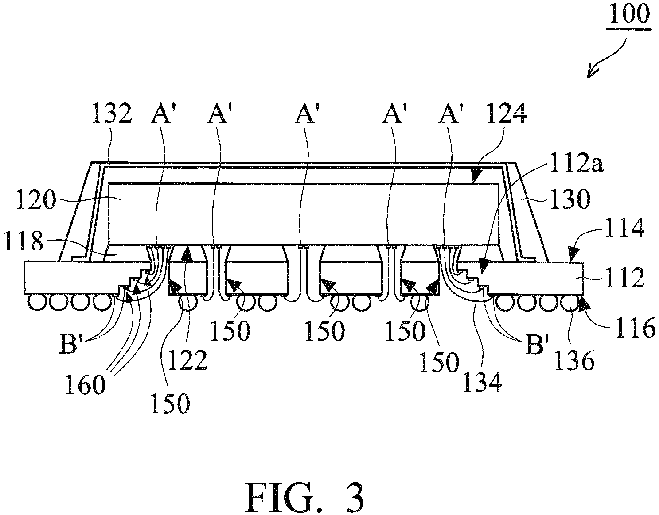
- FIG. 3 shows an exemplary semiconductor package 100 with reduced IR drop effects, comprising a circuit board 112, a semiconductor chip 120, an encapsulant layer 130, a heat spreading layer 132, and a plurality of conductive elements 136.
- the semiconductor chip 120 is, for example, a functional chip such as a microprocessor chip, a memory chip, a logic chip or other functional chips, and has an active first surface 122 and an inactive second surface 124.
- the first surface 122 of the semiconductor chip 120 comprises a plurality of input/output pads A' located adjacent to the peripheral edges of first surface 122.
- the semiconductor chip 120 may be thinned by polishing the second surface 124. In one embodiment, the semiconductor chip 120 may have a thickness of about 4-18 mil.
- the circuit board 112 has opposing first and second surfaces 114 and 116, and the adhesive layer 118 and the semiconductor chip 120 are sequentially formed over the center portion of the first surface 114 of the circuit board 112.
- the circuit board 112 is mainly composed of a resin layer (not shown) formed from BT (bismaleimide triazine) board, FR 4 board, FR 5 board, or some other glass-fiber filled organic (e.g., epoxy) laminate of the type used to make printed circuit board substrates for semiconductor packages.
- BT bismaleimide triazine
- FR 4 board FR 4 board
- FR 5 board or some other glass-fiber filled organic (e.g., epoxy) laminate of the type used to make printed circuit board substrates for semiconductor packages.
- multiple layers of conductive traces and conductive interconnects are also formed in the circuit board 112, thereby providing suitable electrical connections between the semiconductor chip 120 and the conductive elements 136.
- the first adhesive layer 118 may comprise epoxy or the like.
- the semiconductor chip 120 is mounted over a center portion of the circuit board 112 through the first adhesive layer 118, and the first surface 122 of the semiconductor chip 120 faces the circuit board 112.
- the first surface 122 of the semiconductor chip 120 comprises a plurality of input/output pads A' located not only at the peripheral edges of first surface 122 but also at a central portion of the first surface 122.
- a plurality of through holes 150 is provided in the circuit board 112 to form through both center and peripheral portions of the circuit board 112.
- the through holes 150 also form through a portion of the first adhesive layer 118 to expose a plurality of the input/output pads A' formed on the first surface 122 of the semiconductor chip 120.
- the peripheral portion of the circuit board 112 which is close to the peripheral edge of the first surface 122 of the semiconductor chip 120, is designed to include a stair-like portion 112a.
- the stair-like portion 112a has a plurality of sub-layers 160 formed vertically between the first surface 114 and the second surface 116 and exposed by the through hole 150.
- the sub-layers 160 of the stair-like portion 112a are not coplanar with the first surface 114 and the second surface 116 of the circuit board 112.
- the through holes 150 may also expose conductive traces and conductive interconnects (both not shown) formed in the plurality of sub-layers 160 of the circuit board 120, and a plurality of bonding pads B' can be formed on the conductive traces and conductive interconnects (both not shown) formed in each of the plurality of sub-layers 160 of the circuit board 120 exposed by the through holes 150.
- the conductive elements 136 are formed on the second surface 116 of the circuit board 112.
- one or more conductive connections 134 may be provided within the through holes 150 and spans between the input/output pads A' and the bonding pads B' to electrically connect the semiconductor chip 120 with the circuit board 112. As shown in FIG. 3 , the conductive connections 134 may be a bond wire formed of gold or aluminum.
- the encapsulant layer 130 covers the second surface 124 of the semiconductor chip 120 and portions of the heat spreading layer 132, so that a portion of the top surface of the heat spreading layer 132 over the semiconductor chip 20 is exposed.
- the encapsulant layer 130 also fills the space between the heat spreading layer 132 and the heat spreading layer 132.
- the encapsulant layer 130 also fills the through holes 150 and covers the conductive connections 134, the bonding pads B', and the input/output pads A' exposed by the through holes 150.
- the encapsulant layer 130 may be formed by molding and curing a resin material (e.g., epoxy), or by pouring and curing a liquid resin material (e.g., epoxy).
- the heat spreading layer 132 can be formed with, for example, the ⁇ -like shape as shown in FIG. 3 having portions contacting the circuit board 112 and may be formed of copper, aluminum, or another metal alloy.
- the semiconductor chip 120 is mounted over the circuit board 112 by facing the active first surface 122 toward the circuit board 112, so that the heat spreader layer 132 can be directly disposed over the inactive surface 124 of the semiconductor chip 132 without an additional thermal conductive spacer formed therebetween. Accordingly, the thickness of the semiconductor package 100 can be reduced.
- the conductive elements 136 for example, are made of lead tin solder or some other metal, and serve as input/output terminals for the semiconductor package 110.
- the conductive elements 136 are each electrically connected to a respective input/output pad A' of the semiconductor chip 120 through the connective connections 134, and the bonding pads B' formed on the conductive traces and conductive interconnects (both not shown) formed in the sub-layers 160 of the stair-like portion 112a of the circuit board 112 exposed by the through holes 150.
- the conductive elements 136 allow the semiconductor package 110 to be mounted on a motherboard (not shown). Other configurations of input/output terminals are possible.
- IR drop effect in the semiconductor chip 120 can be reduced since additional input/output pad A are provided on at least the central portion of first surface 122, so that connective connections 134 such as bonding wires can be provided between the input/output pad A' of the semiconductor chip 120 on both central and peripheral portions of first surface 122 of the second semiconductor chip 120 and the sub-layers 160 of the stair-like portion 112a of the circuit board 112 exposed by the through holes 150.
- the input/output pad A' are located on both central and peripheral portions of first surface 122 of the semiconductor chip 120, so that interconnect structures provided in the semiconductor chip 120 can be designed with a relatively simple routing structure to link the active or passive components located at the central portion semiconductor chip 120 with the input/output pad A'. Therefore, fabrication of the semiconductor chip 120 can be simplified and the number of input/output pads A' around the peripheral edges of first surface 122 of the semiconductor chip 120 can be decreased even as the trend for forming a more impact of the semiconductor chip 120.
- FIG. 4 shows a schematic plane view of the first surface 122 of the semiconductor chip 120 shown in FIG. 3 . As shown in FIG. 4 , only the input/output pads A' formed on the first surface 122 of the semiconductor chip 120 are illustrated, for the purpose of simplicity.
- loose connective connections 134 can be provided around the peripheral edges of first surface 122 of the semiconductor chip 120 to connect the input/output pads A' of the semiconductor chip 120 with the bonding pads B' formed over the package substrate 112.
- additional input/output pads A' are provided over the central portion of the first surface 122 of the semiconductor chip 120. Therefore, the size of the package 100 can be reduced to accommodate more connections between input/output pads A' and the bonding pads B', which is desired as the trend for shrinking a size of the semiconductor package 100.
- configuration of the input/output pads A' shown in FIGs. 3-4 allows shorter wire loop and IR drop effects can be reduced, so that more flexible IC designs for input/output pads can be achieved.
- FIGs. 5-7 are various embodiments showing the layout of through holes formed in the circuit boards 112, and a second surface 116 of the circuit boards 112 having the bumps 136 formed thereon is illustrated.
- one of the through holes 150 having a rectangular shape is provided as the center of the circuit board 112, and the other through holes 150 form a continuous rectangular trench surrounding the through hole 150 with the rectangular shape and are apart from the through hole 150 with the rectangular shape.
- the through holes 150 are provided as a crisscross configuration on the second surface 116 of the circuit board 112.
- the through holes 150 are provided as a plurality of parallel trenches isolated from each other by the circuit boards 112. As shown in FIG. 7 , one of the through holes 150 can be formed as a first trench and the other through holes can be formed as second trenches at opposite side of the first trench.
- configurations of the through holes 150 can be adjusted further and can be other shapes according to various designs of the input/output pads A' of the semiconductor chip 120, and are not limited by those shown in FIGs. 5-7 .
- a semiconductor package comprising: a circuit board comprising opposite first and second surfaces and a plurality of through holes; a semiconductor chip formed over a center portion of the first surface of the circuit board, having an active surface facing the circuit board; a heat spreading layer formed over the semiconductor chip; an encapsulant layer formed over the circuit board, covering heat spreading layer, the semiconductor chip, and the circuit board; a plurality of conductive connections respectively passing through the through holes and electrically connecting the semiconductor chip with the circuit board; and a plurality of conductive elements formed over the second surface of the circuit board.
- a semiconductor package comprising: a circuit board comprising opposite first and second surfaces and a plurality of through holes; a semiconductor chip formed over a center portion of the first surface of the circuit board, having an active surface facing the circuit board; a heat spreading layer formed over the semiconductor chip; an encapsulant layer formed over the circuit board, covering heat spreading layer, the semiconductor chip, and the circuit board; a plurality of conductive connections respectively passing through the through holes and electrically connecting the semiconductor chip with the circuit board, wherein the circuit board comprises a stair-like portion, wherein the stair-like portion has a plurality of sub-layers formed vertically between the first surface and the second surface of the circuit board and exposed by one the plurality of through holes.
- a semiconductor package comprising: a circuit board comprising opposite first and second surfaces and a plurality of through holes; a semiconductor chip formed over a center portion of the first surface of the circuit board, having an active surface facing the circuit board; a plurality of conductive connections respectively passing through the through holes and electrically connecting the semiconductor chip with the circuit board, wherein the circuit board comprises a stair-like portion, wherein the stair-like portion has a plurality of sub-layers formed vertically between the first surface and the second surface of the circuit board and exposed by one the plurality of through holes, and wherein one of the plurality of conductive connections electrically connects a bonding pad disposed on one of the plurality of sub-layers.
Landscapes
- Engineering & Computer Science (AREA)
- Microelectronics & Electronic Packaging (AREA)
- Structures Or Materials For Encapsulating Or Coating Semiconductor Devices Or Solid State Devices (AREA)
- Physics & Mathematics (AREA)
- Geometry (AREA)
- Chemical & Material Sciences (AREA)
- Materials Engineering (AREA)
- Internal Circuitry In Semiconductor Integrated Circuit Devices (AREA)
- Cooling Or The Like Of Semiconductors Or Solid State Devices (AREA)
Abstract

Description
- This application claims the benefit of
U.S. Provisional Application No. 62/268,624, filed on December 17, 2015 - The present invention relates to integrated circuit (IC) devices, and particularly to a semiconductor package with reduced IR drop effects and more flexible bond-pad designs.
- A typical ball grid array (BGA) semiconductor package includes a semiconductor chip mounted on the upper surface of an insulating printed circuit board substrate. The substrate may be made of a glass-fiber filled organic laminate, such as an FR4 board, FR5 board, or BT board, and have interconnected conductive circuit patterns on the upper and lower surfaces thereof. A hardened encapsulating material covers the chip, the upper surface of the substrate, and electrical conductors, such as bond wires, that extend between the chip and the circuit patterns on the upper surface of the substrate. Conductive balls or other input/output terminals are formed on the circuit patterns of the lower surface of the substrate.
- However, while existing BGA semiconductor packages have been generally adequate for their intended purposes, they have not been entirely satisfactory in every respect.
- An exemplary semiconductor package comprises a circuit board, a semiconductor chip, a heat spreading layer, an encapsulant layer, a plurality of conductive connections , and a plurality of solder balls. The circuit board comprises opposite first and second surfaces and a plurality of through holes. The semiconductor chip is formed over a center portion of the first surface of the circuit board, having an active surface facing the circuit board. The heat spreading layer is formed over the semiconductor chip. The encapsulant layer is formed over the circuit board, covering heat spreading layer, the semiconductor chip, and the circuit board. The plurality of conductive connections respectively pass through the through holes and electrically connecting the semiconductor chip with the circuit board. The plurality of solder balls are formed over the second surface of the circuit board.
- A detailed description is given in the following embodiments with reference to the accompanying drawings.
- The invention can be more fully understood by reading the subsequent detailed description and examples with references made to the accompanying drawings, wherein:
-
FIG. 1 is a schematic cross section of a semiconductor package in accordance with an embodiment of the present invention; -
FIG. 2 is a schematic top view of the semiconductor package shown inFIG. 1 ; -
FIG. 3 is a schematic cross section of a semiconductor package in accordance with another embodiment of the present invention; -
FIG. 4 is a schematic plane view of the semiconductor chip shown inFIG. 4 ; and -
FIGs. 5-7 are schematic bottom views of the circuit board shown inFIG. 3 . - The following description is of the best-contemplated mode of carrying out the invention. This description is made for the purpose of illustrating the general principles of the invention and should not be taken in a limiting sense. The scope of the invention is best determined by reference to the appended claims.
-
FIG. 1 shows a schematic cross section of anexemplary semiconductor package 10, comprising acircuit board 12, asemiconductor chip 20, aspacer 28, anencapsulant layer 30, aheat spreading layer 32, and a plurality ofconductive elements 36. - As shown in
FIG. 1 , thesemiconductor chip 20 is, for example, a functional chip such as a microprocessor chip, a memory chip, a logic chip or other functional chips, and has an activefirst surface 22 and an inactivesecond surface 24. Thefirst surface 22 of thesemiconductor chip 20 comprises a plurality of input/output pads A located adjacent to the peripheral edges offirst surface 22. Thesemiconductor chip 20 may be thinned by polishing thesecond surface 24. In one embodiment, thesemiconductor chip 20 may have a thickness of about 4-8 mil. - The
semiconductor chip 20 is mounted over a center portion of thecircuit board 12 through a firstadhesive layer 18. Thecircuit board 12 has opposing first andsecond surfaces adhesive layer 18 and thesemiconductor chip 20 are sequentially formed over the center portion of thefirst surface 14 of thecircuit board 12. Thecircuit board 12 is mainly composed of a resin layer (not shown) formed from BT (bismaleimide triazine) board, FR 4 board, FR 5 board, or some other glass-fiber filled organic (e.g., epoxy) laminate of the type used to make printed circuit board substrates for semiconductor packages. In addition, conductive traces and conductive interconnects (both not shown) are also formed in thecircuit board 12, thereby providing suitable electrical connections between thesemiconductor chip 20 and theconductive elements 36. The firstadhesive layer 18 may comprise epoxy or the like. - As shown in
FIG. 1 , a plurality of bonding pads B and electrically conductive circuit patterns (not shown) are formed on thefirst surface 14 of thecircuit board 12, and theconductive elements 36 are formed on thesecond surface 16 of thecircuit board 12. Each input/output pad A of thesemiconductor chip 20 is electrically connected to one of the bonding pads B by aconductive connection 34, which spans between thesemiconductor chip 20 and the bonding pads. As shown inFIG. 1 , theconductive connection 34 may be a bond wire formed of gold or aluminum. - In addition, the
spacer 28 is mounted over a center portion of thefirst surface 22 of thesemiconductor chip 20 through a second adhesive layer 26. Thespacer 28, for example, is a rectangular non-functional chip made of a blank semiconductor wafer, and may comprise a semiconductor material which is the same as that of the semiconductor layer (not shown) of thesemiconductor chip 20. Thespacer 28 is formed with a cross-sectional dimension, for example a width W1 that is smaller than that of the cross-sectional dimension, or a width W2 of thesemiconductor chip 20. In one embodiment, thespacer 28 is formed with a thickness of about 4-10 mil. - The
encapsulant layer 30 covers thefirst surface 22 of thesemiconductor chip 20, portions of thefirst surface 14 of thecircuit board 12, and portions of theheat spreading layer 32, so that a portion of the top surface of theheat spreading layer 32 over the spacer 26 and thesemiconductor chip 20 is exposed. Theencapsulant layer 30 also fills the space between theheat spreading layer 32 and the spacer 26 and theheat spreading layer 32. Theencapsulant layer 30 may be formed by molding and curing a resin material (e.g., epoxy), or by pouring and curing a liquid resin material (e.g., epoxy). Theheat spreading layer 32 can be formed with, for example, the Ω-like shape shown inFIG. 1 having portions contacting thecircuit board 12 and may be formed of copper, aluminum, or another metal alloy. - The
conductive elements 36, for example, are made of lead tin solder or some other metal, and serve as input/output (I/O) terminals for thesemiconductor package 10. Theconductive elements 36 are each electrically connected to a respective input/output pad A of thesemiconductor chip 20 through theconnective connections 34, the bonding pad B formed over thecircuit board 12, and the conductive traces and conductive interconnects (both not shown) formed in thecircuit board 12. Theconductive elements 36 allow thesemiconductor package 10 to be mounted on a motherboard (not shown). Other configurations of input/output terminals are possible. -
FIG. 2 shows a schematic top view of thesemiconductor package 10 shown inFIG. 1, and FIG. 1 shows the schematic cross section taken along line 1-1 inFIG. 2 . InFIG. 2 , theheat spreading layer 32 and theencapsulant layer 30 are not shown, and thecircuit board 12, thesemiconductor chip 20, thespacer 28 and theconnective connections 34 are illustrated, for the purpose of simplicity. - As shown in
FIG. 2 , theconnective connections 34 are provided on thefirst surface 22 of thesemiconductor chip 20 for electrically connecting the input/output pads A formed around the peripheral edges of thesemiconductor chip 20 with the bonding pads B formed over thefirst surface 12 of thepackage substrate 12. - In the
exemplary semiconductor package 10 shown inFIGs. 1-2 , since the input/output pads A are all located on thefirst surface 22 of thesemiconductor chip 20 around the peripheral edges thereof, so that theconductive connections 34 will be provided between the input/output pads A of thesemiconductor chip 20 and the bonding pads B formed over thepackage substrate 12 in a dense configuration. Therefore, thesemiconductor chip 20 will be provided with a larger size for accommodating more input/output pads A of thesemiconductor chip 20 and preventing short-circuits between the adjacentconductive connections 34, as the trend for increasing the number of active or passive components within thesemiconductor chip 20. - In addition, since all the input/output pads A are on the
first surface 22 of thesemiconductor chip 20 around the peripheral edges thereof, thesemiconductor chip 20 needs to be formed with even more complex interconnect structures to link active or passive components located at, for example, a central portion of thesemiconductor chip 20 with the input/output pads A, meaning that fabrication of thesemiconductor chip 20 will become more complex and the length of the path between the active or passive components formed in thesemiconductor chip 20 and the input/output pad A around the peripheral edges of thefirst surface 22 of thesemiconductor chip 20 may be too long. Therefore, undesired IR drop effects may happen to the active or passive components located at, for example, the central portion in thesemiconductor chip 20 ofsemiconductor package 10 and performances of thesemiconductor package 10 is thus affected. - Thus, an improved semiconductor package with reduced IR drop effects is needed.
-
FIG. 3 shows anexemplary semiconductor package 100 with reduced IR drop effects, comprising acircuit board 112, asemiconductor chip 120, anencapsulant layer 130, aheat spreading layer 132, and a plurality ofconductive elements 136. - As shown in
FIG. 3 , thesemiconductor chip 120 is, for example, a functional chip such as a microprocessor chip, a memory chip, a logic chip or other functional chips, and has an activefirst surface 122 and an inactivesecond surface 124. Thefirst surface 122 of thesemiconductor chip 120 comprises a plurality of input/output pads A' located adjacent to the peripheral edges offirst surface 122. Thesemiconductor chip 120 may be thinned by polishing thesecond surface 124. In one embodiment, thesemiconductor chip 120 may have a thickness of about 4-18 mil. - The
circuit board 112 has opposing first andsecond surfaces adhesive layer 118 and thesemiconductor chip 120 are sequentially formed over the center portion of thefirst surface 114 of thecircuit board 112. Thecircuit board 112 is mainly composed of a resin layer (not shown) formed from BT (bismaleimide triazine) board, FR 4 board, FR 5 board, or some other glass-fiber filled organic (e.g., epoxy) laminate of the type used to make printed circuit board substrates for semiconductor packages. In addition, multiple layers of conductive traces and conductive interconnects (both not shown) are also formed in thecircuit board 112, thereby providing suitable electrical connections between thesemiconductor chip 120 and theconductive elements 136. The firstadhesive layer 118 may comprise epoxy or the like. - As shown in
FIG. 3 , thesemiconductor chip 120 is mounted over a center portion of thecircuit board 112 through the firstadhesive layer 118, and thefirst surface 122 of thesemiconductor chip 120 faces thecircuit board 112. Thefirst surface 122 of thesemiconductor chip 120 comprises a plurality of input/output pads A' located not only at the peripheral edges offirst surface 122 but also at a central portion of thefirst surface 122. - In addition, a plurality of through
holes 150 is provided in thecircuit board 112 to form through both center and peripheral portions of thecircuit board 112. In addition, the throughholes 150 also form through a portion of the firstadhesive layer 118 to expose a plurality of the input/output pads A' formed on thefirst surface 122 of thesemiconductor chip 120. As shown inFIG. 3 , the peripheral portion of thecircuit board 112, which is close to the peripheral edge of thefirst surface 122 of thesemiconductor chip 120, is designed to include a stair-like portion 112a. The stair-like portion 112a has a plurality ofsub-layers 160 formed vertically between thefirst surface 114 and thesecond surface 116 and exposed by the throughhole 150. Also, thesub-layers 160 of the stair-like portion 112a are not coplanar with thefirst surface 114 and thesecond surface 116 of thecircuit board 112. The throughholes 150 may also expose conductive traces and conductive interconnects (both not shown) formed in the plurality ofsub-layers 160 of thecircuit board 120, and a plurality of bonding pads B' can be formed on the conductive traces and conductive interconnects (both not shown) formed in each of the plurality ofsub-layers 160 of thecircuit board 120 exposed by the throughholes 150. Theconductive elements 136 are formed on thesecond surface 116 of thecircuit board 112. - Moreover, one or more
conductive connections 134 may be provided within the throughholes 150 and spans between the input/output pads A' and the bonding pads B' to electrically connect thesemiconductor chip 120 with thecircuit board 112. As shown inFIG. 3 , theconductive connections 134 may be a bond wire formed of gold or aluminum. - In addition, the
encapsulant layer 130 covers thesecond surface 124 of thesemiconductor chip 120 and portions of theheat spreading layer 132, so that a portion of the top surface of theheat spreading layer 132 over thesemiconductor chip 20 is exposed. Theencapsulant layer 130 also fills the space between theheat spreading layer 132 and theheat spreading layer 132. In addition, theencapsulant layer 130 also fills the throughholes 150 and covers theconductive connections 134, the bonding pads B', and the input/output pads A' exposed by the throughholes 150. Theencapsulant layer 130 may be formed by molding and curing a resin material (e.g., epoxy), or by pouring and curing a liquid resin material (e.g., epoxy). Theheat spreading layer 132 can be formed with, for example, the Ω-like shape as shown inFIG. 3 having portions contacting thecircuit board 112 and may be formed of copper, aluminum, or another metal alloy. - As shown in
FIG. 3 , since thesemiconductor chip 120 is mounted over thecircuit board 112 by facing the activefirst surface 122 toward thecircuit board 112, so that theheat spreader layer 132 can be directly disposed over theinactive surface 124 of thesemiconductor chip 132 without an additional thermal conductive spacer formed therebetween. Accordingly, the thickness of thesemiconductor package 100 can be reduced. In addition, theconductive elements 136, for example, are made of lead tin solder or some other metal, and serve as input/output terminals for the semiconductor package 110. Theconductive elements 136 are each electrically connected to a respective input/output pad A' of thesemiconductor chip 120 through theconnective connections 134, and the bonding pads B' formed on the conductive traces and conductive interconnects (both not shown) formed in thesub-layers 160 of the stair-like portion 112a of thecircuit board 112 exposed by the throughholes 150. Theconductive elements 136 allow the semiconductor package 110 to be mounted on a motherboard (not shown). Other configurations of input/output terminals are possible. - In the
exemplary semiconductor package 100 shown inFIG. 3 , IR drop effect in thesemiconductor chip 120 can be reduced since additional input/output pad A are provided on at least the central portion offirst surface 122, so thatconnective connections 134 such as bonding wires can be provided between the input/output pad A' of thesemiconductor chip 120 on both central and peripheral portions offirst surface 122 of thesecond semiconductor chip 120 and thesub-layers 160 of the stair-like portion 112a of thecircuit board 112 exposed by the throughholes 150. - Moreover, since the input/output pad A' are located on both central and peripheral portions of
first surface 122 of thesemiconductor chip 120, so that interconnect structures provided in thesemiconductor chip 120 can be designed with a relatively simple routing structure to link the active or passive components located at the centralportion semiconductor chip 120 with the input/output pad A'. Therefore, fabrication of thesemiconductor chip 120 can be simplified and the number of input/output pads A' around the peripheral edges offirst surface 122 of thesemiconductor chip 120 can be decreased even as the trend for forming a more impact of thesemiconductor chip 120. -
FIG. 4 shows a schematic plane view of thefirst surface 122 of thesemiconductor chip 120 shown inFIG. 3 . As shown inFIG. 4 , only the input/output pads A' formed on thefirst surface 122 of thesemiconductor chip 120 are illustrated, for the purpose of simplicity. - As shown in
FIG. 4 , loose connective connections 134 (seeFIG. 3 ) can be provided around the peripheral edges offirst surface 122 of thesemiconductor chip 120 to connect the input/output pads A' of thesemiconductor chip 120 with the bonding pads B' formed over thepackage substrate 112. In addition, since additional input/output pads A' are provided over the central portion of thefirst surface 122 of thesemiconductor chip 120. Therefore, the size of thepackage 100 can be reduced to accommodate more connections between input/output pads A' and the bonding pads B', which is desired as the trend for shrinking a size of thesemiconductor package 100. - Moreover, in the
semiconductor package 100, configuration of the input/output pads A' shown inFIGs. 3-4 allows shorter wire loop and IR drop effects can be reduced, so that more flexible IC designs for input/output pads can be achieved. -
FIGs. 5-7 are various embodiments showing the layout of through holes formed in thecircuit boards 112, and asecond surface 116 of thecircuit boards 112 having thebumps 136 formed thereon is illustrated. - As shown in
FIG. 5 , one of the throughholes 150 having a rectangular shape is provided as the center of thecircuit board 112, and the other throughholes 150 form a continuous rectangular trench surrounding the throughhole 150 with the rectangular shape and are apart from the throughhole 150 with the rectangular shape. - In addition, as shown in
FIG. 6 , the throughholes 150 are provided as a crisscross configuration on thesecond surface 116 of thecircuit board 112. - Moreover, as shown in
FIG. 7 , the throughholes 150 are provided as a plurality of parallel trenches isolated from each other by thecircuit boards 112. As shown inFIG. 7 , one of the throughholes 150 can be formed as a first trench and the other through holes can be formed as second trenches at opposite side of the first trench. - In other embodiments, configurations of the through
holes 150 can be adjusted further and can be other shapes according to various designs of the input/output pads A' of thesemiconductor chip 120, and are not limited by those shown inFIGs. 5-7 . - While the invention has been described by way of example and in terms of the preferred embodiments, it is to be understood that the invention is not limited to the disclosed embodiments. On the contrary, it is intended to cover various modifications and similar arrangements (as would be apparent to those skilled in the art). Therefore, the scope of the appended claims should be accorded the broadest interpretation so as to encompass all such modifications and similar arrangements.
- For example, a semiconductor package can be provided, the semiconductor package comprising: a circuit board comprising opposite first and second surfaces and a plurality of through holes; a semiconductor chip formed over a center portion of the first surface of the circuit board, having an active surface facing the circuit board; a heat spreading layer formed over the semiconductor chip; an encapsulant layer formed over the circuit board, covering heat spreading layer, the semiconductor chip, and the circuit board; a plurality of conductive connections respectively passing through the through holes and electrically connecting the semiconductor chip with the circuit board; and a plurality of conductive elements formed over the second surface of the circuit board.
- According to another example, a semiconductor package can be provided, the semiconductor package comprising: a circuit board comprising opposite first and second surfaces and a plurality of through holes; a semiconductor chip formed over a center portion of the first surface of the circuit board, having an active surface facing the circuit board; a heat spreading layer formed over the semiconductor chip; an encapsulant layer formed over the circuit board, covering heat spreading layer, the semiconductor chip, and the circuit board; a plurality of conductive connections respectively passing through the through holes and electrically connecting the semiconductor chip with the circuit board, wherein the circuit board comprises a stair-like portion, wherein the stair-like portion has a plurality of sub-layers formed vertically between the first surface and the second surface of the circuit board and exposed by one the plurality of through holes.
- According to further example, a semiconductor package can be provided, the semiconductor package comprising: a circuit board comprising opposite first and second surfaces and a plurality of through holes; a semiconductor chip formed over a center portion of the first surface of the circuit board, having an active surface facing the circuit board; a plurality of conductive connections respectively passing through the through holes and electrically connecting the semiconductor chip with the circuit board, wherein the circuit board comprises a stair-like portion, wherein the stair-like portion has a plurality of sub-layers formed vertically between the first surface and the second surface of the circuit board and exposed by one the plurality of through holes, and wherein one of the plurality of conductive connections electrically connects a bonding pad disposed on one of the plurality of sub-layers.
Claims (15)
- A semiconductor package, comprising:a circuit board comprising opposite first and second surfaces and a plurality of through holes;a semiconductor chip formed over a center portion of the first surface of the circuit board, having an active surface facing the circuit board;a heat spreading layer formed over the semiconductor chip;an encapsulant layer formed over the circuit board, covering heat spreading layer, the semiconductor chip, and the circuit board;a plurality of conductive connections respectively passing through the through holes and electrically connecting the semiconductor chip with the circuit board;
anda plurality of conductive elements formed over the second surface of the circuit board. - The semiconductor package as claimed in claim 1, wherein the encapsulant layer does not physically contact the active surface of semiconductor chip.
- The semiconductor package as claimed in claim 1 or claim 2, further comprising a first adhesive layer formed between the first surface of the circuit board and the active surface of the semiconductor chip.
- The semiconductor package as claimed in one of the preceding claims, wherein the encapsulant layer is further formed between the heat spreading layer and the semiconductor chip.
- The semiconductor package as claimed in one of the preceding claims, wherein the semiconductor chip is a functional chip.
- The semiconductor package as claimed in one of the preceding claims, wherein the heat spreading layer comprises copper or aluminum.
- The semiconductor package as claimed in one of the preceding claims, wherein the encapsulant layer comprises resin material.
- The semiconductor package as claimed in one of the preceding claims, further comprising another encapsulant layer fills the through holes and covers the conductive connections.
- The semiconductor package as claimed in one of the preceding claims, wherein the through holes comprise a first through hole exposing a center portion of the active surface of the semiconductor chip and a plurality of second through holes exposing a peripheral portion of the active surface of the semiconductor chip.
- The semiconductor package as claimed in claim 9, wherein the circuit board comprises a stair-like portion, wherein the stair-like portion has a plurality of sub-layers formed vertically between the first surface and the second surface of the circuit board and exposed by one of the plurality of second through holes.
- The semiconductor package as claimed in claim 10, wherein the stair-like portion is positioned in a peripheral portion of the circuit board, which is close to the peripheral portion of the active surface of the semiconductor chip.
- The semiconductor package as claimed in one of the claims 9 to 11, wherein the second through holes are formed at a side of the first through hole; and/or
wherein the first through hole is formed as a first trench and the second through holes are formed as second trenches at opposite sides of the first trench on the second surface of the circuit board;
wherein the first and second through holes are formed with a crisscross configuration on the second surface of the circuit board;
wherein the first through hole comprises a rectangular through hole and the second through hole forms a continuous rectangular trench surrounding the first through hole on the second surface of the circuit board. - The semiconductor package as claimed in one of the claims 9 to 12, wherein the plurality of sub-layers of the stair-like portion is exposed by one of the plurality of second through holes.
- The semiconductor package as claimed in one of the claims 9 to 13,
wherein the sub-layers of the stair-like portion are not coplanar with the first surface and the second surface of the circuit board. - The semiconductor package as claimed in one of the claims 9 to 14,
wherein one of the plurality of conductive connections electrically connects a bonding pad disposed on one of the plurality of sub-layers.
Applications Claiming Priority (2)
| Application Number | Priority Date | Filing Date | Title |
|---|---|---|---|
| US201562268624P | 2015-12-17 | 2015-12-17 | |
| US15/349,113 US10008441B2 (en) | 2015-12-17 | 2016-11-11 | Semiconductor package |
Publications (1)
| Publication Number | Publication Date |
|---|---|
| EP3182449A1 true EP3182449A1 (en) | 2017-06-21 |
Family
ID=57442546
Family Applications (1)
| Application Number | Title | Priority Date | Filing Date |
|---|---|---|---|
| EP16201345.2A Withdrawn EP3182449A1 (en) | 2015-12-17 | 2016-11-30 | Semiconductor package |
Country Status (4)
| Country | Link |
|---|---|
| US (1) | US10008441B2 (en) |
| EP (1) | EP3182449A1 (en) |
| CN (1) | CN107039390A (en) |
| TW (1) | TWI613771B (en) |
Cited By (1)
| Publication number | Priority date | Publication date | Assignee | Title |
|---|---|---|---|---|
| IT201900009660A1 (en) * | 2019-06-20 | 2020-12-20 | St Microelectronics Srl | SEMICONDUCTOR INTEGRATED DEVICE AND PROCEDURE FOR MANUFACTURING AN INTEGRATED SEMICONDUCTOR DEVICE |
Families Citing this family (2)
| Publication number | Priority date | Publication date | Assignee | Title |
|---|---|---|---|---|
| KR102600154B1 (en) * | 2019-06-12 | 2023-11-07 | 삼성전자주식회사 | Semiconductor package |
| US11945714B2 (en) * | 2020-07-30 | 2024-04-02 | Stmicroelectronics S.R.L. | Electronic device and corresponding method |
Citations (6)
| Publication number | Priority date | Publication date | Assignee | Title |
|---|---|---|---|---|
| JPS61137335A (en) * | 1984-12-10 | 1986-06-25 | Toshiba Corp | Semiconductor device |
| JPH11297738A (en) * | 1998-04-06 | 1999-10-29 | Denso Corp | Semiconductor chip mounting structure |
| US6445594B1 (en) * | 2000-02-10 | 2002-09-03 | Mitsubishi Denki Kabushiki Kaisha | Semiconductor device having stacked semiconductor elements |
| US20070080466A1 (en) * | 2005-10-07 | 2007-04-12 | Shih-Wen Chou | Universal chip package structure |
| JP2009231296A (en) * | 2008-03-19 | 2009-10-08 | Powertech Technology Inc | Heat radiation type multiple hole semiconductor package |
| KR20100053189A (en) * | 2008-11-12 | 2010-05-20 | 삼성테크윈 주식회사 | Semiconductor package |
Family Cites Families (4)
| Publication number | Priority date | Publication date | Assignee | Title |
|---|---|---|---|---|
| CN100490131C (en) * | 2006-12-21 | 2009-05-20 | 力成科技股份有限公司 | Ball grid array package structure for preventing glue overflow |
| US9252092B2 (en) * | 2013-07-24 | 2016-02-02 | Stats Chippac, Ltd. | Semiconductor device and method of forming through mold hole with alignment and dimension control |
| KR101546575B1 (en) * | 2013-08-12 | 2015-08-21 | 앰코 테크놀로지 코리아 주식회사 | Semiconductor Package And Fabricating Method Thereof |
| US9881861B2 (en) * | 2014-05-28 | 2018-01-30 | Ngk Spark Plug Co., Ltd. | Wiring substrate |
-
2016
- 2016-11-11 US US15/349,113 patent/US10008441B2/en active Active
- 2016-11-15 CN CN201611032531.4A patent/CN107039390A/en active Pending
- 2016-11-30 EP EP16201345.2A patent/EP3182449A1/en not_active Withdrawn
- 2016-12-16 TW TW105141745A patent/TWI613771B/en not_active IP Right Cessation
Patent Citations (6)
| Publication number | Priority date | Publication date | Assignee | Title |
|---|---|---|---|---|
| JPS61137335A (en) * | 1984-12-10 | 1986-06-25 | Toshiba Corp | Semiconductor device |
| JPH11297738A (en) * | 1998-04-06 | 1999-10-29 | Denso Corp | Semiconductor chip mounting structure |
| US6445594B1 (en) * | 2000-02-10 | 2002-09-03 | Mitsubishi Denki Kabushiki Kaisha | Semiconductor device having stacked semiconductor elements |
| US20070080466A1 (en) * | 2005-10-07 | 2007-04-12 | Shih-Wen Chou | Universal chip package structure |
| JP2009231296A (en) * | 2008-03-19 | 2009-10-08 | Powertech Technology Inc | Heat radiation type multiple hole semiconductor package |
| KR20100053189A (en) * | 2008-11-12 | 2010-05-20 | 삼성테크윈 주식회사 | Semiconductor package |
Cited By (2)
| Publication number | Priority date | Publication date | Assignee | Title |
|---|---|---|---|---|
| IT201900009660A1 (en) * | 2019-06-20 | 2020-12-20 | St Microelectronics Srl | SEMICONDUCTOR INTEGRATED DEVICE AND PROCEDURE FOR MANUFACTURING AN INTEGRATED SEMICONDUCTOR DEVICE |
| US11069587B2 (en) | 2019-06-20 | 2021-07-20 | Stmicroelectronics S.R.L. | Integrated semiconductor device and process for manufacturing an integrated semiconductor device |
Also Published As
| Publication number | Publication date |
|---|---|
| US20170179017A1 (en) | 2017-06-22 |
| TW201733048A (en) | 2017-09-16 |
| US10008441B2 (en) | 2018-06-26 |
| TWI613771B (en) | 2018-02-01 |
| CN107039390A (en) | 2017-08-11 |
Similar Documents
| Publication | Publication Date | Title |
|---|---|---|
| US12057366B2 (en) | Semiconductor devices including a lower semiconductor package, an upper semiconductor package on the lower semiconductor package, and a connection pattern between the lower semiconductor package and the upper semiconductor package | |
| KR102734944B1 (en) | Semiconductor package | |
| US10734367B2 (en) | Semiconductor package and method of fabricating the same | |
| US7687899B1 (en) | Dual laminate package structure with embedded elements | |
| KR100626618B1 (en) | Semiconductor chip stack package and manufacturing method | |
| US8269323B2 (en) | Integrated circuit package with etched leadframe for package-on-package interconnects | |
| US7763964B2 (en) | Semiconductor device and semiconductor module using the same | |
| US6812567B2 (en) | Semiconductor package and package stack made thereof | |
| US10923428B2 (en) | Semiconductor package having second pad electrically connected through the interposer chip to the first pad | |
| KR102587976B1 (en) | Semiconductor packages | |
| KR20070054553A (en) | Semiconductor package and manufacturing method thereof | |
| US10008441B2 (en) | Semiconductor package | |
| KR102387541B1 (en) | Semiconductor chip, and flip chip package and wafer level package including the same | |
| US20080164620A1 (en) | Multi-chip package and method of fabricating the same | |
| US11670574B2 (en) | Semiconductor device | |
| CN117936500A (en) | Electronic package and manufacturing method thereof and substrate structure | |
| TWI423405B (en) | Package structure with carrier | |
| KR20120126365A (en) | Unit package and stack package having the same | |
| KR102549402B1 (en) | Semiconductor package and method for fabricating the same | |
| US20250349699A1 (en) | Wiring substrate and semiconductor package including the same | |
| JP2013110264A (en) | Semiconductor device and semiconductor device manufacturing method | |
| KR101001638B1 (en) | Semiconductor package | |
| KR20100050981A (en) | Semiconductor package and stack package using the same | |
| KR100813621B1 (en) | Stacked Semiconductor Device Package |
Legal Events
| Date | Code | Title | Description |
|---|---|---|---|
| PUAI | Public reference made under article 153(3) epc to a published international application that has entered the european phase |
Free format text: ORIGINAL CODE: 0009012 |
|
| STAA | Information on the status of an ep patent application or granted ep patent |
Free format text: STATUS: THE APPLICATION HAS BEEN PUBLISHED |
|
| AK | Designated contracting states |
Kind code of ref document: A1 Designated state(s): AL AT BE BG CH CY CZ DE DK EE ES FI FR GB GR HR HU IE IS IT LI LT LU LV MC MK MT NL NO PL PT RO RS SE SI SK SM TR |
|
| AX | Request for extension of the european patent |
Extension state: BA ME |
|
| STAA | Information on the status of an ep patent application or granted ep patent |
Free format text: STATUS: REQUEST FOR EXAMINATION WAS MADE |
|
| 17P | Request for examination filed |
Effective date: 20171215 |
|
| RBV | Designated contracting states (corrected) |
Designated state(s): AL AT BE BG CH CY CZ DE DK EE ES FI FR GB GR HR HU IE IS IT LI LT LU LV MC MK MT NL NO PL PT RO RS SE SI SK SM TR |
|
| STAA | Information on the status of an ep patent application or granted ep patent |
Free format text: STATUS: EXAMINATION IS IN PROGRESS |
|
| 17Q | First examination report despatched |
Effective date: 20200304 |
|
| P01 | Opt-out of the competence of the unified patent court (upc) registered |
Effective date: 20230607 |
|
| STAA | Information on the status of an ep patent application or granted ep patent |
Free format text: STATUS: THE APPLICATION IS DEEMED TO BE WITHDRAWN |
|
| 18D | Application deemed to be withdrawn |
Effective date: 20240103 |