EP3179530A2 - Display device and fabricating method thereof - Google Patents
Display device and fabricating method thereof Download PDFInfo
- Publication number
- EP3179530A2 EP3179530A2 EP16201360.1A EP16201360A EP3179530A2 EP 3179530 A2 EP3179530 A2 EP 3179530A2 EP 16201360 A EP16201360 A EP 16201360A EP 3179530 A2 EP3179530 A2 EP 3179530A2
- Authority
- EP
- European Patent Office
- Prior art keywords
- film
- pads
- layer
- display device
- film layer
- Prior art date
- Legal status (The legal status is an assumption and is not a legal conclusion. Google has not performed a legal analysis and makes no representation as to the accuracy of the status listed.)
- Granted
Links
Images





Classifications
-
- H—ELECTRICITY
- H10—SEMICONDUCTOR DEVICES; ELECTRIC SOLID-STATE DEVICES NOT OTHERWISE PROVIDED FOR
- H10K—ORGANIC ELECTRIC SOLID-STATE DEVICES
- H10K59/00—Integrated devices, or assemblies of multiple devices, comprising at least one organic light-emitting element covered by group H10K50/00
- H10K59/10—OLED displays
- H10K59/12—Active-matrix OLED [AMOLED] displays
- H10K59/131—Interconnections, e.g. wiring lines or terminals
-
- H—ELECTRICITY
- H10—SEMICONDUCTOR DEVICES; ELECTRIC SOLID-STATE DEVICES NOT OTHERWISE PROVIDED FOR
- H10K—ORGANIC ELECTRIC SOLID-STATE DEVICES
- H10K50/00—Organic light-emitting devices
- H10K50/80—Constructional details
- H10K50/84—Passivation; Containers; Encapsulations
- H10K50/844—Encapsulations
-
- H—ELECTRICITY
- H10—SEMICONDUCTOR DEVICES; ELECTRIC SOLID-STATE DEVICES NOT OTHERWISE PROVIDED FOR
- H10K—ORGANIC ELECTRIC SOLID-STATE DEVICES
- H10K59/00—Integrated devices, or assemblies of multiple devices, comprising at least one organic light-emitting element covered by group H10K50/00
- H10K59/10—OLED displays
- H10K59/12—Active-matrix OLED [AMOLED] displays
-
- H—ELECTRICITY
- H10—SEMICONDUCTOR DEVICES; ELECTRIC SOLID-STATE DEVICES NOT OTHERWISE PROVIDED FOR
- H10K—ORGANIC ELECTRIC SOLID-STATE DEVICES
- H10K59/00—Integrated devices, or assemblies of multiple devices, comprising at least one organic light-emitting element covered by group H10K50/00
- H10K59/10—OLED displays
- H10K59/12—Active-matrix OLED [AMOLED] displays
- H10K59/123—Connection of the pixel electrodes to the thin film transistors [TFT]
-
- H—ELECTRICITY
- H10—SEMICONDUCTOR DEVICES; ELECTRIC SOLID-STATE DEVICES NOT OTHERWISE PROVIDED FOR
- H10K—ORGANIC ELECTRIC SOLID-STATE DEVICES
- H10K59/00—Integrated devices, or assemblies of multiple devices, comprising at least one organic light-emitting element covered by group H10K50/00
- H10K59/80—Constructional details
- H10K59/87—Passivation; Containers; Encapsulations
- H10K59/873—Encapsulations
-
- H—ELECTRICITY
- H10—SEMICONDUCTOR DEVICES; ELECTRIC SOLID-STATE DEVICES NOT OTHERWISE PROVIDED FOR
- H10K—ORGANIC ELECTRIC SOLID-STATE DEVICES
- H10K71/00—Manufacture or treatment specially adapted for the organic devices covered by this subclass
-
- H—ELECTRICITY
- H10—SEMICONDUCTOR DEVICES; ELECTRIC SOLID-STATE DEVICES NOT OTHERWISE PROVIDED FOR
- H10K—ORGANIC ELECTRIC SOLID-STATE DEVICES
- H10K59/00—Integrated devices, or assemblies of multiple devices, comprising at least one organic light-emitting element covered by group H10K50/00
- H10K59/10—OLED displays
- H10K59/12—Active-matrix OLED [AMOLED] displays
- H10K59/1201—Manufacture or treatment
Definitions
- the present invention relates to a display device and a fabricating method thereof.
- LCD liquid crystal display
- PDP plasma display panel
- organic light emitting display device With the advancement of an information society, a demand for a display device for displaying an image has increased in various forms. Recently, various flat panel display devices such as a liquid crystal display (LCD), a plasma display panel (PDP), and an organic light emitting display device have been used.
- LCD liquid crystal display
- PDP plasma display panel
- organic light emitting display device an organic light emitting display device
- the display device includes a display panel and a data driver.
- the display panel includes a display area and a non-display area.
- the display area includes data lines, gate lines, and a plurality of pixels formed at crossing portions between the data lines and the gate lines and supplied with data voltages of the data lines when gate signals are supplied to the gate lines.
- the pixels emit light with a predetermined brightness in accordance with the data voltages, and an encapsulation layer for protecting the pixels from oxygen and water may be formed above the display area.
- the non-display area is formed in the periphery of the display area.
- the data driver may include a plurality of source drive integrated circuits (hereinafter, referred to as "ICs"). Each of the source drive ICs may be fabricated of a driving chip. Each of the source drive ICs may be packaged in a flexible film. Each of source flexible films may be embodied in a tape carrier package or chip on film (COF), and may be bent or curved.
- ICs source drive integrated circuits
- Each of the flexible films may be attached to pads formed on the non-display area by using an anisotropic conductive film (ACF). Since the pads are electrically connected with the data lines, the source drive ICs may be connected with the data lines.
- ACF anisotropic conductive film
- the anisotropic conductive film when the anisotropic conductive film is attached to the pads, the anisotropic conductive film cannot be attached to the pads if the encapsulation layer is formed on the pads. Therefore, the encapsulation layer is formed on a light emitting layer only using a mask, and is patterned so as not to be formed on the pads.
- the pads may be opened through dry-etching, or may be opened by laser ablation for the area where the pads are formed.
- EPL etching protection layer
- the present invention is directed to a display device and a fabricating method thereof, which substantially obviate one or more problems due to limitations and disadvantages of the related art.
- An advantage of the present invention is to provide a display device and a fabricating method thereof, in which an organic-inorganic composite film is patterned without a mask by using an anti-film layer, whereby the cost may be reduced.
- a display device comprises a lower substrate; pixels arranged on a display area of the lower substrate; pads arranged on a non-display area of the lower substrate; an encapsulation layer arranged on the pixels; and an anti-film layer arranged on the pads as a molecular layer having a thickness of a single molecule.
- a fabricating method of a display device comprises the steps of forming pads on a non-display area of a lower substrate and forming pixels on a display area; and forming an anti-film layer on the pixels as a molecular layer having a thickness of a single molecule.
- one or more portions may be arranged between two other portions unless 'just' or 'direct' is used.
- X-axis direction should not be construed by a geometric relation only of a mutual vertical relation, and may have broader directionality within the range that elements of the present disclosure may act functionally.
- At least one should be understood as including any and all combinations of one or more of the associated listed items.
- the meaning of "at least one of a first item, a second item, and a third item” denotes the combination of all items proposed from two or more of the first item, the second item, and the third item as well as the first item, the second item, or the third item.
- X-axis direction indicates a direction parallel with a gate line
- Y-axis indicates a direction parallel with a data line
- Z-axis indicates a height direction of the display device.
- the display device has been described based on an organic light emitting display device, the display device may be realized as a liquid crystal display device or an electrophoresis display device.
- the display device includes a display panel 10, a gate driver 20, a source drive integrated circuit (hereinafter, referred to as "IC") 30, a flexible film 40, a circuit board 50, and a timing controller 60.
- IC source drive integrated circuit
- the display panel 10 includes a lower substrate 100 and an upper substrate 190.
- the lower substrate 100 serves as a support substrate.
- the upper substrate 190 serves as an encapsulation substrate.
- the display panel 10 transmits incident light or displays an image.
- Gate lines and data lines may be formed on a display area DA of the display panel 10, and pixels may be formed on crossing areas where the gate lines cross the data lines.
- the pixels of the display area DA may display an image.
- the gate driver 20 supplies gate signals to the gate lines in accordance with a gate control signal input from the timing controller 60.
- the gate driver 20 is formed, but not limited to, outside one side of the display area DA of the display panel 10 in a gate driver in panel (GIP) mode. That is, the gate driver 20 may be formed outside both sides of the display area DA of the display panel 10 in a GIP mode, or may be fabricated of a driving chip, packaged in a flexible film and attached to the display panel 10 in a tape automated bonding (TAB) mode.
- GIP gate driver in panel
- the source drive IC 30 receives digital video data and a source control signal from the timing controller 60.
- the source drive IC 30 converts the digital video data to analog data voltages in accordance with the source control signal and supplies the analog data voltages to the data lines. If the source drive IC 30 is fabricated of a driving chip, the source drive IC 30 may be packaged in the flexible film 40 in a chip on film (COF) or chip on plastic (COP) mode.
- COF chip on film
- COP chip on plastic
- Pads such as data pads are provided in a part of the lower substrate 100. Lines which connect the pads with the source drive IC 30 and lines which connect the pads with lines of the circuit board 50 may be formed in the flexible film 40.
- the flexible film 40 is attached on the pads by using an anisotropic conductive film, whereby the pads may be connected with the lines of the flexible film 40.
- the circuit board 50 may be attached to the flexible films 40.
- a plurality of circuits comprised of driving chips may be packaged in the circuit board 50.
- the timing controller 60 may be packaged in the circuit board 50.
- the circuit board 50 may be a printed circuit board or a flexible printed circuit board.
- the timing controller 60 receives digital video data and a timing signal from an external system board (not shown).
- the timing controller 60 generates a gate control signal for controlling an operation timing of the gate driver 20 and a source control signal for controlling the source drive ICs 30 on the basis of the timing signal.
- the timing controller 60 supplies the gate control signal to the gate driver 20, and supplies the source control signal to the source drive ICs 30.
- FIG. 2 is a front view illustrating a display device.
- a display area DA a display area DA, a non-display area NDA, a pad area PAD, pads 200, and an anti-film layer 300 are shown.
- the display area DA indicates an area where an image is displayed. Pixels are formed on the display area DA. A detailed description of the pixels will be described later with reference to FIG. 3 .
- the non-display area NDA is formed outside the display area DA.
- the non-display area NDA may include pads 200 for supplying a gate voltage and a data voltage to the pixels arranged within the display area DA.
- the pad area PAD where the pads 200 are formed is formed on a part of the non-display area NDA.
- the pad area PAD is formed below the non-display area NDA.
- the pads 200 are formed on the pad area PAD of the lower substrate 100.
- the pads 200 shown in FIG. 2 supply a data voltage to the display area DA.
- the anti-film layer 300 is formed on the pads 200.
- the anti-film layer 300 may be formed above the pads 200 and on the pad area PAD.
- the anti-film layer 300 may be arranged above all the pads 200.
- the anti-film layer 300 may prevent an inorganic protection film or an inorganic-organic composite film from being formed on the pads 200.
- the inorganic protection film or the inorganic-organic composite film is formed to protect the device from an external environment, especially water and oxygen.
- the pads 200 which should be electrically connected with an external circuit should be maintained in a state that the inorganic protection film or the inorganic-organic composite film is not formed, that is, should be opened.
- the anti-film layer 300 may be used instead of the mask in the present disclosure such that the inorganic protection film or the inorganic-organic composite film may not be formed above the pads 200.
- the pads 200 may be fabricated to be electrically connected with each other even in a device in which a mask is not used, among inorganic film devices, and the pads 200 may be fabricated to be electrically connected with each other without a mask even in a device in which a mask may be used, whereby the mask cost and management cost may be reduced.
- FIG. 3 is a cross-sectional view illustrating a display device.
- FIG. 3 illustrates a cross-sectional view taken along line I-I' of FIG. 2 .
- the display device according to the first embodiment of the present disclosure has been described based on an organic light emitting display device in FIG. 3
- the display device may be realized as a liquid crystal display device or an electrophoresis display device. A part of the display area DA and the pad area PAD are shown in FIG. 3 .
- Pixels P are formed on the display area DA.
- a cross-section of one of the pixels P is shown in FIG. 3 .
- the pixel P indicates an area that includes an anode electrode 151 exposed between banks 154, an organic light emitting layer 153 provided on the anode electrode 151, and a thin film transistor 110 of which drain electrode 114 is connected with the anode electrode 151.
- Each of the thin film transistors 110 includes a semiconductor layer 111, a gate electrode 112, a source electrode 113, and a drain electrode 114.
- the semiconductor layers 111 are provided on the lower substrate 100.
- a buffer film may be provided between the lower substrate 100 and the semiconductor layers 111.
- An inter layer dielectric 120 may be provided on the semiconductor layers 111.
- a gate electrode 112 may be provided on the inter layer dielectric 120.
- a gate insulating film 130 may be provided on the gate electrodes 112.
- the source electrodes 113 and the drain electrodes 114 may be provided on the gate insulating film 130. Each of the source electrodes 113 and the drain electrodes 114 may be connected to the semiconductor layer 111 through a contact hole that passes through the inter layer dielectric 120 and the gate insulating film 130.
- a planarization film 140 is provided on the thin film transistor 110 to arrange the pixels P, which are partitioned by banks 154, with planarization.
- Anode electrodes 151, organic light emitting layers 153, a cathode electrode 152, and the banks 154 are provided on the planarization film 140.
- the anode electrodes 151 and the organic light emitting layers 153 may be provided on the display area DA, and the cathode electrode 152 and the banks 154 may be provided on the display area DA and the non-display area NDA.
- Each of the anode electrodes 151 is connected to the drain electrode 114 through a contact hole that passes through the planarization film 140.
- the organic light emitting layers 153 are provided on the anode electrodes 151 exposed between the banks 154 on the display area DA. Since each of the banks 154 is higher than each of the organic light emitting layers 153, the organic light emitting layers 153 are partitioned by the banks 154. That is, each of the organic light emitting layers 153 is arranged between the banks 154.
- the cathode electrode 152 is provided on the organic light emitting layers 153 and the banks 154 in the display area DA to cover the organic light emitting layers 153 and the banks 154.
- An encapsulation layer 170 is provided on the cathode electrode 152.
- the encapsulation layer 170 serves to prevent oxygen or water from being permeated into the organic light emitting layers 153 and the cathode electrode 152.
- the encapsulation layer 170 includes a first inorganic film 171, an organic film 172, and a second inorganic film 173.
- the first inorganic film 171 is provided on the cathode electrode 152 to cover the cathode electrode 152.
- the organic film 172 is provided on the first inorganic film 171 to prevent water and oxygen from being permeated into the organic light emitting layer 153 and the cathode electrode 152 by passing through the first inorganic film 171.
- the second inorganic film 173 is provided on the organic film 172 to cover the organic film 172.
- Each of the first and second inorganic films 171 and 173 may be formed of silicon nitride, aluminum nitride, titanium nitride, silicon oxide, aluminum oxide or titanium oxide.
- each of the first and second inorganic films 171 and 173 may be formed SiNx, SiO 2 , Al 2 O 3 , or TiO 2 .
- FIG. 4 is an enlarged view illustrating pads 200, an anti-film material 300, an anisotropic conductive film ACF 400 and a flexible film 40.
- the pads 200 are provided on a part of the lower substrate 100.
- the pads 200 may be gate pads supplying the gate control signal to the gate driver, data pads supplying the data voltage to the data lines, or power pads supplying a power voltage to a power line.
- the pads 200 are arranged on the pad area PAD of the lower substrate 100 as shown in FIGS. 3 and 4 .
- the pads 200 may be arranged on the gate insulating film 130 formed on the lower substrate 100.
- the pads 200 may be arranged to be connected with a conductive line formed on the lower substrate 100 by passing through the gate insulating film 130.
- the anti-film material 310 is a material for forming the anti-film layer 300.
- the anti-film material 310 is arranged above the pads 200 and the pad area PAD.
- the anti-film material 310 may be a self-assembled monolayer (SAM) of which molecules are self-aligned in accordance with affinity of its adjacent material.
- the anti-film layer 300 may have a thickness the same as a length of one molecule of the anti-film material 310.
- the anisotropic conductive film ACF 400 may allow the flexible film 40 to be connected with the pad 200.
- the anisotropic conductive film ACF 400 may have a plurality of conductive balls 401 having high electrical conductivity.
- the conductive ball 401 may be formed between the anti-film materials 310 or may be formed to pass through the anti-film layer 300. Therefore, the pad 200 may electrically be connected with the flexible film 40 through the conductive ball 401 even in the case that the anti-film layer 300 is formed.
- the flexible film 40 is attached onto the pads 200 by using the anisotropic conductive film ACF 400.
- the lines connecting the pads 200 with the source drive IC and the lines connecting the pads 200 with the lines of the circuit board may be formed in the flexible film 40.
- the pads 200 may be connected with the source drive IC or the circuit board through the lines formed in the flexible film 40.
- the flexible film 40 may package the source drive IC in a chip on film (COF) mode.
- COF chip on film
- FIG. 5 is a structural view illustrating a molecule of an anti-film material 310.
- the anti-film material 310 includes a head part 311, a chain 312, and a tail part 313.
- the head part 311 is bonded to an upper surface of the pads 200.
- the head part 311 is made of thiol, silane, or phosphonic acid, which may easily be bonded (by a covalent or ionic bond, or other bonding mechanism) or otherwise adsorbed or bound, to a conductive metal formed on the upper surface of the pads 200.
- the chain 312 is extended from one side of the head part 311.
- the chain 312 is made of hydrocarbon as a main material. If a reaction of hydrocarbon that forms the chain 312 is controlled to adjust a length of the chain 312, a length of the anti-film layer 310 may be adjusted.
- the anti-film layer 300 is a molecular layer having a thickness of a single molecule. Since the anti-film layer 300 forms a layer using one of molecules of the anti-film material 310, the length of the chain 312 may be adjusted to adjust the thickness of the anti-film layer 300.
- the tail part 313 is connected to an end at one side of the chain 312.
- the tail part 313 is formed at an opposite side of the head part 311 to prevent the first inorganic film 171, the organic film 172 and the second inorganic film 173 from being formed on the pads 200.
- the tail part 313 is made of methyl which is not reacted with the first inorganic film 171, the organic film 172 and the second inorganic film 173.
- the anti-film layer 300 is formed on the pads 200, whereby the encapsulation layer 170 is not formed. For this reason, a separate mask for removing the encapsulation layer 170 formed on the pads 200 may not be used. Therefore, the mask cost and the cost for performing a patterning process using a mask may be reduced.
- the anti-film layer 300 remains on the pads 200. For this reason, water and oxygen may be prevented from being permeated into the pads 200 during the process.
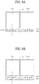
- FIGS. 6A and 6B A display area DA, a non-display area NDA, a pad area PAD, pads 200, and an anti-film layer 300 are shown in FIGS. 6A and 6B . Pixels are formed on the display area DA of the display device. Since the display area DA, the pixels, the non-display area NDA, the pad area PAD, and the pads 200 according to the second embodiment are the same as those of the display device according to the first embodiment, their detailed description will be omitted.
- the anti-film layer 300 according to the second embodiment of the present invention may be arranged to cover the non-display area NDA without being formed to be limited to the pad area PAD of the pads 200.
- the anti-film layer 300 may be arranged to cover the whole non-display area NDA.
- the first inorganic film 171, the organic film 172, and the second inorganic film 173 are formed in the display area DA only. Therefore, the encapsulation layer 170 is formed separately per display panel 10.
- the encapsulation layer 170 is uniformly arranged on a plurality of display panels 10. Therefore, after the encapsulation layer 170 is arranged, the encapsulation layer 170 is cut during a scribing (S) process for cutting per display panel 10.
- the deposition structure of the first inorganic film 171, the organic film 172 and the second inorganic film 173, which are formed at the edge of each display panel 10 and constitute the encapsulation layer 170 may be distorted, or the encapsulation layer 170 may be peeled away. Oxygen and water may be permeated into the display panel 10, in which the deposition structure of the encapsulation layer 170 is distorted or peeled away, through the edge of the display panel 10.
- the encapsulation layer 170 is not formed on the non-display area NDA. That is, the encapsulation layer 170 is formed separately per display panel 10, and is not formed on the cross-section where the scribing (S) is performed as shown in FIG. 6B . Therefore, the deposition structure of the first inorganic film 171, the organic film 172 and the second inorganic film 173, which are arranged within the encapsulation layer 170 formed on the display panel 10, may be neither distorted nor peeled away, whereby oxygen and water are not permeated into the edge of the display panel 10.
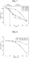
- the principle and effect of the anti-film layer 300 may be noted through a resultant graph of FIG. 7 .
- FIG. 7 is a resultant graph of an experiment that measures a contact angle to measure anti-film property of aluminum oxide (Al 2 O 3 ). It is noted that aluminum oxide is deposited on the surface of the anti-film layer 300 if the contact angle becomes small. The contact angle becomes small if a process cycle is continued. On the contrary, an anti-film prevention effect is continued if the contact angle becomes great.
- ODPA Oxydiphthalic Anhydride
- ODTS Oxctadecyltrichlorosilane
- ODPA of which the chain 312 is formed of 18 carbon atoms has an anti-film prevention effect superior to that of DDPA (Dimethy-diphenylphosphinamide) of which the chain 312 is formed of 12 carbon atoms.
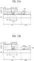
- FIGS. 12 and 13A to 13D a fabricating method of a display device will be described with reference to FIGS. 12 and 13A to 13D .
- the pads 200 are formed on the non-display area NDA of the lower substrate 100.
- the thin film transistors 110, the inter layer dielectric 120 and the gate insulating film 130 may be formed on the lower substrate 100 before the pads 200 are formed on the non-display area NDA.
- the anode electrodes 151 and the banks 154 may be formed on the thin film transistor (TFT) 110 before, after or at the same time when the pads 200 are formed. (S101 of FIG. 12 )
- the anti-film layer 300 is formed on the pads 200 as a molecular layer having a thickness of a single molecule.
- the anti-film material 310 may be dipped on the pad area PAD or stamped on the pads 200. Afterwards, the anti-film material 310 may be dried.
- the anti-film material 310 may be dipped on the pad area PAD or stamped on the pads 200 such that the anti-film layer 300 may only be formed above the pads and on the pad area PAD. (S102 of FIG. 12 )
- the anti-film material 310 may be sprayed onto the entire non-display area NDA, whereby the anti-film layer 300 may be formed to cover the non-display area NDA. That is, since the anti-film layer 300 may be formed on a desired area without using a mask, the process cost required to use the mask may be reduced. (S102 of FIG. 12 )
- the organic light emitting layer 153 and the cathode electrode 152 are formed.
- the organic light emitting layers 153 are formed on the anode electrode 151 exposed between the banks 154 on the display area DA.
- the cathode electrode 152 is formed on the organic light emitting layers 153 and the banks 154 on the display area DA to cover the organic light emitting layers 153 and the banks 154. (S103 of FIG. 12 ).
- the first inorganic film 171, the organic film 172 and the second inorganic film 173 are covered.
- the first inorganic film 172 is formed on the cathode electrode 152 of the display area DA and the bank 154 of the non-display area NDA.
- the organic film 172 is formed on the first inorganic film 171 of the display area DA to prevent water and oxygen from being permeated into the organic light emitting layer 153 and the cathode electrode 152 by passing through the first inorganic film 171.
- the second inorganic film 173 is formed on the organic film 172.
- the second inorganic film 173 may cover the first inorganic film 171 and the organic film 172.
- a process method for forming the encapsulation layer 170 according to the fabricating method of the display device is atomic layer deposition (ALD).
- the atomic layer deposition includes spraying a precursor, which may be deposited through a chemical reaction, to be deposited on the display panel 100 in an atomic unit and removing the other precursors, which are not deposited in an atomic unit through a chemical reaction, that is, precursors physically attached onto the display panel, through a purge process.
- the encapsulation layer 170 may be formed on the display panel 100 in an atomic unit by spraying a reactant. Residual materials which are not deposited in an atomic unit are removed again through a purge process.
- Examples of factors that the inorganic protection film or the inorganic-organic composite film is not formed on the anti-film layer 300 even without using a mask may include a material type and thickness of the anti-film layer 300, a pressure that may enable a chemical deposition of a precursor, and a pressure of a purge process for removing materials physically deposited after being reacted with a reactant.
- FIG. 8 is a resultant graph illustrating an anti-film effect measured per pressure of a precursor.
- a TMA pressure shown in FIG. 8 is the pressure that the precursor is sprayed onto the display panel 100 to form an aluminum oxide inorganic layer.
- the anti-film layer 300 formed on the pads 200 may prevent the precursor from being deposited, if the precursor is deposited at high pressure, the precursor is formed even on the anti-film layer 300, and a reactant is formed on the precursor, whereby a problem occurs in that the encapsulation layer 170 is formed on an area where the encapsulation layer 170 should not be formed. Therefore, it is preferable that the precursor is formed at a pressure that allows the precursor not to be formed on the anti-film layer 300.
- FIG. 9 is a resultant graph illustrating an anti-film effect measured per pressure of a purge process for removing materials where deposition is generated.
- the purge process is performed using an inert gas such as argon (Ar). Residual precursors and reactant may be removed efficiently such that the purge process may be performed at high pressure.
- FIGS. 10 and 11 are graphs illustrating a pressure when a precursor is formed and anti-film efficiency based on a pressure during a purge process. (S104 of FIG. 12 )
- each of the pads 200 is connected with the flexible film 40.
- the flexible film 40 may be a chip on film (COF).
- COF chip on film
- Each of the pads 200 is connected with the flexible film 40 in a state that the anti-film layer 300 is arranged above the pads 200.
- the anisotropic conductive film ACF 400 is used to electrically connect the flexible film 40 with the each of the pads 200.
- the anti-film layer 300 remains on the pads 200 in the range of 100nm or less. Since the conductive balls 401 within the anisotropic conductive film 400 are arranged to partially pass through the anti-film layer 300, the pads 200 may electrically be connected with the flexible film 40 in a state that the anti-film layer 300 is arranged between the pads 200. (S105 of FIG. 12 )
- the display device and the fabricating method thereof may obtain the following advantages as follows.
- the anti-film layer is formed on the pads, whereby the encapsulation layer is not formed. For this reason, a separate mask for removing the encapsulation layer formed on the pads may not be used. Therefore, the mask cost and the cost for performing a patterning process using a mask may be reduced.
- the anti-film layer remains on the pads. For this reason, water and oxygen may be prevented from being permeated into the pads during the process.
- the deposition structure of the first inorganic film, the organic film and the second inorganic film, which are formed at the edge of the display panel may be neither distorted nor peeled away even though the scribing process is performed, whereby oxygen and water may be prevented from being permeated into the edge of the display panel.
- the anti-film layer is formed on the pads such that the protection layer is not formed for electric connection of the pads, whereby the inorganic film made of aluminum oxide (AlOx) may be prevented from being formed. Therefore, in a semiconductor equipment and the fabricating method of the display device, atomic layer deposition may be performed using aluminum oxide to prevent the inorganic film made of aluminum oxide from being formed.
- a pressure is adjusted such that a precursor is not formed on the anti-film layer during an integrated circuit and semiconductor process based on atomic layer deposition.
- a purge process for removing the precursor or a reactant is performed at a pressure stronger than that applied when the precursor is formed to remove materials which are deposited. Therefore, when the integrated circuit and semiconductor process based on atomic layer deposition is performed, since a mask for preventing the protection layer from being formed for electric connection on the circuit is not required, the process cost may be reduced.
- a display device comprising: a lower substrate; pixels arranged on a display area of the lower substrate; pads arranged on a non-display area of the lower substrate; an encapsulation layer arranged on the pixels; and an anti-film layer arranged on the pads as a single molecular layer.
- Clause 3 The display device of clause 1, wherein the anti-film layer is arranged to cover the non-display area.
- each of the pads is electrically connected with an anisotropic conductive film arranged on the anti-film layer.
- an anti-film material constituting the anti-film layer includes: a head part bonded to a surface of the pads; a chain extended from one side of the head part; and a tail part connected to an end at one side of the chain, the head part is made of thiol, silane or phosphonic acid, and the tail part is made of methyl.
- a fabricating method of a display device comprising the steps of: forming pads on a non-display area of a lower substrate and forming pixels on a display area; and forming an anti-film layer on the pixels as a single molecular layer.
- Clause 7 The fabricating method of clause 6, wherein the step of forming the anti-film layer includes: dipping an anti-film material on the pads or stamping the anti-film material on the pads; and drying the anti-film material.
- Clause 8 The fabricating method of clause 6, further comprising the step of forming an encapsulation layer on a display panel on which the anti-film layer is formed, without a mask, wherein the encapsulation layer is not formed on the anti-film layer, and is formed using atomic layer deposition, and the atomic layer deposition includes forming an inorganic material at a first pressure, and purging the other inorganic material except an inorganic material deposited in an atomic unit, at a second pressure higher than the first pressure.
- Clause 10 The fabricating method of clause 6, wherein the step of forming the anti-film layer includes forming the anti-film layer on the pads in the range of 100nm or less.
Landscapes
- Engineering & Computer Science (AREA)
- Microelectronics & Electronic Packaging (AREA)
- Manufacturing & Machinery (AREA)
- Physics & Mathematics (AREA)
- Optics & Photonics (AREA)
- Electroluminescent Light Sources (AREA)
- Devices For Indicating Variable Information By Combining Individual Elements (AREA)
Abstract
Description
- This application claims the priority benefit of the
Korean Patent Application No. 10-2015-0168701, filed on November 30, 2015 - The present invention relates to a display device and a fabricating method thereof.
- With the advancement of an information society, a demand for a display device for displaying an image has increased in various forms. Recently, various flat panel display devices such as a liquid crystal display (LCD), a plasma display panel (PDP), and an organic light emitting display device have been used.
- The display device includes a display panel and a data driver. The display panel includes a display area and a non-display area. The display area includes data lines, gate lines, and a plurality of pixels formed at crossing portions between the data lines and the gate lines and supplied with data voltages of the data lines when gate signals are supplied to the gate lines. The pixels emit light with a predetermined brightness in accordance with the data voltages, and an encapsulation layer for protecting the pixels from oxygen and water may be formed above the display area. The non-display area is formed in the periphery of the display area.
- The data driver may include a plurality of source drive integrated circuits (hereinafter, referred to as "ICs"). Each of the source drive ICs may be fabricated of a driving chip. Each of the source drive ICs may be packaged in a flexible film. Each of source flexible films may be embodied in a tape carrier package or chip on film (COF), and may be bent or curved.
- Each of the flexible films may be attached to pads formed on the non-display area by using an anisotropic conductive film (ACF). Since the pads are electrically connected with the data lines, the source drive ICs may be connected with the data lines.
- Meanwhile, when the anisotropic conductive film is attached to the pads, the anisotropic conductive film cannot be attached to the pads if the encapsulation layer is formed on the pads. Therefore, the encapsulation layer is formed on a light emitting layer only using a mask, and is patterned so as not to be formed on the pads.
- Alternatively, if the mask is not used, after an etching protection layer (EPL) is formed on an area except the area where the pads are formed, the pads may be opened through dry-etching, or may be opened by laser ablation for the area where the pads are formed.
- It takes additional cost as the mask process is increased if the mask is used. And it takes additional cost for forming the etching protection layer even when the mask is not used.
- Accordingly, the present invention is directed to a display device and a fabricating method thereof, which substantially obviate one or more problems due to limitations and disadvantages of the related art.
- An advantage of the present invention is to provide a display device and a fabricating method thereof, in which an organic-inorganic composite film is patterned without a mask by using an anti-film layer, whereby the cost may be reduced.
- Additional advantages and features of the invention will be set forth in part in the description which follows and in part will become apparent to those having ordinary skill in the art upon examination of the following or may be learned from practice of the invention. The objectives and other advantages of the invention may be realized and attained by the structure particularly pointed out in the written description and claims hereof as well as the appended drawings.
- To achieve these objects and other advantages and in accordance with the purpose of the invention, as embodied and broadly described herein, a display device according to the embodiment of the present invention comprises a lower substrate; pixels arranged on a display area of the lower substrate; pads arranged on a non-display area of the lower substrate; an encapsulation layer arranged on the pixels; and an anti-film layer arranged on the pads as a molecular layer having a thickness of a single molecule.
- In another aspect of the present invention, a fabricating method of a display device according to the embodiment of the present invention comprises the steps of forming pads on a non-display area of a lower substrate and forming pixels on a display area; and forming an anti-film layer on the pixels as a molecular layer having a thickness of a single molecule.
- It is to be understood that both the foregoing general description and the following detailed description of the present invention are exemplary and explanatory and are intended to provide further explanation of the invention as claimed.
- The accompanying drawings, which are included to provide a further understanding of the disclosure and are incorporated in and constitute a part of this application, illustrate embodiment(s) of the invention and together with the description serve to explain the principle of the disclosure. In the drawings:
-
FIG. 1 is a plane view illustrating a display panel, a gate driver, a source drive IC, a flexible film, a circuit board and a timing controller of a display device; -
FIG. 2 is a plane view illustrating an encapsulation layer, pads and an anti-film layer of a display device; -
FIG. 3 is a cross-sectional view taken along line I-I' ofFIG. 2 ; -
FIG. 4 is an enlarged view illustrating pads, an anti-film material, an anisotropic conductive film and a flexible film; -
FIG. 5 is a structural view illustrating a molecule of an anti-film material ofFIG. 4 ; -
FIGS. 6A and 6B are plane views illustrating an encapsulation layer, pads and an anti-film layer prior to cutting of a display device; -
FIG. 7 is a graph illustrating the principle and effect of an anti-film layer of a display device; -
FIGS. 8 to 11 are graphs illustrating an effect based on variables of a fabricating method of a display device; -
FIG. 12 is a flow chart illustrating a fabricating method of a display device; and -
FIGS. 13A to 13D are cross-sectional views illustrating a fabricating method of a display device. - Advantages and features of the present invention, and implementation methods thereof will be clarified through following embodiments described with reference to the accompanying drawings. The present invention may, however, be embodied in different forms and should not be construed as limited to the embodiments set forth herein. Rather, these embodiments are provided so that this disclosure will be thorough and complete, and will fully convey the scope of the present invention to those skilled in the art. Further, the present invention is defined by the scope of the claims.
- A shape, a size, a ratio, an angle, and a number disclosed in the drawings are merely an example, and thus, the present disclosure is not limited to the illustrated details. Like reference numerals refer to like elements throughout the specification. In the following description, when the detailed description of the relevant known function or configuration is determined to unnecessarily obscure the important point of the present disclosure, the detailed description will be omitted.
- In a case where 'comprise', 'have', and 'include' described in the present specification are used, another part may be added unless 'only∼' is used. The terms of a singular form may include plural forms unless referred to the contrary.
- In construing an element, the element is construed as including an error range although there is no explicit description.
- In describing a position relationship, for example, when the position relationship is described as 'upon∼', 'above∼', 'below∼', and 'next to∼', one or more portions may be arranged between two other portions unless 'just' or 'direct' is used.
- In describing a time relationship, for example, when the temporal order is described as 'after∼', 'subsequent∼', 'next∼', and 'before∼', a case which is not continuous may be included unless 'just' or 'direct' is used.
- It will be understood that, although the terms "first", "second", etc. may be used herein to describe various elements, these elements should not be limited by these terms. These terms are only used to distinguish one element from another element. Therefore, a first element could be termed a second element, and, similarly, a second element could be termed a first element, without departing from the scope of the present disclosure.
- "X-axis direction", "Y-axis direction" and "Z-axis direction" should not be construed by a geometric relation only of a mutual vertical relation, and may have broader directionality within the range that elements of the present disclosure may act functionally.
- The term "at least one" should be understood as including any and all combinations of one or more of the associated listed items. For example, the meaning of "at least one of a first item, a second item, and a third item" denotes the combination of all items proposed from two or more of the first item, the second item, and the third item as well as the first item, the second item, or the third item.
- Features may be partially or overall coupled to or combined with each other, and may be variously inter-operated with each other and driven technically as those skilled in the art can sufficiently understand. The embodiments may be carried out independently from each other, or may be carried out together in co-dependent relationship.
- Hereinafter, the embodiments will be described in detail with reference to the accompanying drawings.
- Hereinafter, a display device will be described in detail with reference to
FIGS. 1 to 7 . For convenience of description inFIGS. 1 to 7 , X-axis direction indicates a direction parallel with a gate line, Y-axis indicates a direction parallel with a data line, and Z-axis indicates a height direction of the display device. - Although the display device according to the embodiment of the present disclosure has been described based on an organic light emitting display device, the display device may be realized as a liquid crystal display device or an electrophoresis display device.
- Referring to
FIG. 1 , the display device includes adisplay panel 10, agate driver 20, a source drive integrated circuit (hereinafter, referred to as "IC") 30, aflexible film 40, acircuit board 50, and atiming controller 60. - The
display panel 10 includes alower substrate 100 and anupper substrate 190. Thelower substrate 100 serves as a support substrate. Theupper substrate 190 serves as an encapsulation substrate. - The
display panel 10 transmits incident light or displays an image. Gate lines and data lines may be formed on a display area DA of thedisplay panel 10, and pixels may be formed on crossing areas where the gate lines cross the data lines. The pixels of the display area DA may display an image. - The
gate driver 20 supplies gate signals to the gate lines in accordance with a gate control signal input from thetiming controller 60. InFIG. 1 , thegate driver 20 is formed, but not limited to, outside one side of the display area DA of thedisplay panel 10 in a gate driver in panel (GIP) mode. That is, thegate driver 20 may be formed outside both sides of the display area DA of thedisplay panel 10 in a GIP mode, or may be fabricated of a driving chip, packaged in a flexible film and attached to thedisplay panel 10 in a tape automated bonding (TAB) mode. - The source drive
IC 30 receives digital video data and a source control signal from thetiming controller 60. Thesource drive IC 30 converts the digital video data to analog data voltages in accordance with the source control signal and supplies the analog data voltages to the data lines. If the source driveIC 30 is fabricated of a driving chip, thesource drive IC 30 may be packaged in theflexible film 40 in a chip on film (COF) or chip on plastic (COP) mode. - Pads such as data pads are provided in a part of the
lower substrate 100. Lines which connect the pads with thesource drive IC 30 and lines which connect the pads with lines of thecircuit board 50 may be formed in theflexible film 40. Theflexible film 40 is attached on the pads by using an anisotropic conductive film, whereby the pads may be connected with the lines of theflexible film 40. - The
circuit board 50 may be attached to theflexible films 40. A plurality of circuits comprised of driving chips may be packaged in thecircuit board 50. For example, thetiming controller 60 may be packaged in thecircuit board 50. Thecircuit board 50 may be a printed circuit board or a flexible printed circuit board. - The
timing controller 60 receives digital video data and a timing signal from an external system board (not shown). Thetiming controller 60 generates a gate control signal for controlling an operation timing of thegate driver 20 and a source control signal for controlling the source driveICs 30 on the basis of the timing signal. Thetiming controller 60 supplies the gate control signal to thegate driver 20, and supplies the source control signal to the source driveICs 30. - Hereinafter, a display will be described with reference to
FIGS. 2 to 5 . -
FIG. 2 is a front view illustrating a display device. InFIG. 2 , a display area DA, a non-display area NDA, a pad area PAD,pads 200, and ananti-film layer 300 are shown. - The display area DA indicates an area where an image is displayed. Pixels are formed on the display area DA. A detailed description of the pixels will be described later with reference to
FIG. 3 . - The non-display area NDA is formed outside the display area DA. The non-display area NDA may include
pads 200 for supplying a gate voltage and a data voltage to the pixels arranged within the display area DA. - The pad area PAD where the
pads 200 are formed is formed on a part of the non-display area NDA. InFIG. 2 , the pad area PAD is formed below the non-display area NDA. Thepads 200 are formed on the pad area PAD of thelower substrate 100. Thepads 200 shown inFIG. 2 supply a data voltage to the display area DA. - The
anti-film layer 300 is formed on thepads 200. In the display device, theanti-film layer 300 may be formed above thepads 200 and on the pad area PAD. Theanti-film layer 300 may be arranged above all thepads 200. Theanti-film layer 300 may prevent an inorganic protection film or an inorganic-organic composite film from being formed on thepads 200. - The inorganic protection film or the inorganic-organic composite film is formed to protect the device from an external environment, especially water and oxygen. However, the
pads 200 which should be electrically connected with an external circuit should be maintained in a state that the inorganic protection film or the inorganic-organic composite film is not formed, that is, should be opened. - Although a mask has been conventionally used to open the inorganic protection film or the inorganic-organic composite film, the
anti-film layer 300 may be used instead of the mask in the present disclosure such that the inorganic protection film or the inorganic-organic composite film may not be formed above thepads 200. - Therefore, the
pads 200 may be fabricated to be electrically connected with each other even in a device in which a mask is not used, among inorganic film devices, and thepads 200 may be fabricated to be electrically connected with each other without a mask even in a device in which a mask may be used, whereby the mask cost and management cost may be reduced. -
FIG. 3 is a cross-sectional view illustrating a display device.FIG. 3 illustrates a cross-sectional view taken along line I-I' ofFIG. 2 . Although the display device according to the first embodiment of the present disclosure has been described based on an organic light emitting display device inFIG. 3 , the display device may be realized as a liquid crystal display device or an electrophoresis display device. A part of the display area DA and the pad area PAD are shown inFIG. 3 . - Pixels P are formed on the display area DA. A cross-section of one of the pixels P is shown in
FIG. 3 . As shown inFIG. 3 , the pixel P indicates an area that includes ananode electrode 151 exposed betweenbanks 154, an organiclight emitting layer 153 provided on theanode electrode 151, and athin film transistor 110 of which drainelectrode 114 is connected with theanode electrode 151. Each of thethin film transistors 110 includes asemiconductor layer 111, agate electrode 112, asource electrode 113, and adrain electrode 114. - The semiconductor layers 111 are provided on the
lower substrate 100. A buffer film may be provided between thelower substrate 100 and the semiconductor layers 111. Aninter layer dielectric 120 may be provided on the semiconductor layers 111. Agate electrode 112 may be provided on theinter layer dielectric 120. Agate insulating film 130 may be provided on thegate electrodes 112. Thesource electrodes 113 and thedrain electrodes 114 may be provided on thegate insulating film 130. Each of thesource electrodes 113 and thedrain electrodes 114 may be connected to thesemiconductor layer 111 through a contact hole that passes through theinter layer dielectric 120 and thegate insulating film 130. - A
planarization film 140 is provided on thethin film transistor 110 to arrange the pixels P, which are partitioned bybanks 154, with planarization. -
Anode electrodes 151, organiclight emitting layers 153, acathode electrode 152, and thebanks 154 are provided on theplanarization film 140. Theanode electrodes 151 and the organiclight emitting layers 153 may be provided on the display area DA, and thecathode electrode 152 and thebanks 154 may be provided on the display area DA and the non-display area NDA. - Each of the
anode electrodes 151 is connected to thedrain electrode 114 through a contact hole that passes through theplanarization film 140. - The organic
light emitting layers 153 are provided on theanode electrodes 151 exposed between thebanks 154 on the display area DA. Since each of thebanks 154 is higher than each of the organiclight emitting layers 153, the organiclight emitting layers 153 are partitioned by thebanks 154. That is, each of the organiclight emitting layers 153 is arranged between thebanks 154. - The
cathode electrode 152 is provided on the organiclight emitting layers 153 and thebanks 154 in the display area DA to cover the organiclight emitting layers 153 and thebanks 154. - An
encapsulation layer 170 is provided on thecathode electrode 152. Theencapsulation layer 170 serves to prevent oxygen or water from being permeated into the organiclight emitting layers 153 and thecathode electrode 152. Theencapsulation layer 170 includes a firstinorganic film 171, anorganic film 172, and a secondinorganic film 173. - The first
inorganic film 171 is provided on thecathode electrode 152 to cover thecathode electrode 152. Theorganic film 172 is provided on the firstinorganic film 171 to prevent water and oxygen from being permeated into the organiclight emitting layer 153 and thecathode electrode 152 by passing through the firstinorganic film 171. The secondinorganic film 173 is provided on theorganic film 172 to cover theorganic film 172. - Each of the first and second
inorganic films inorganic films -
FIG. 4 is an enlargedview illustrating pads 200, ananti-film material 300, an anisotropicconductive film ACF 400 and aflexible film 40. - The
pads 200 are provided on a part of thelower substrate 100. Thepads 200 may be gate pads supplying the gate control signal to the gate driver, data pads supplying the data voltage to the data lines, or power pads supplying a power voltage to a power line. Thepads 200 are arranged on the pad area PAD of thelower substrate 100 as shown inFIGS. 3 and 4 . Thepads 200 may be arranged on thegate insulating film 130 formed on thelower substrate 100. Thepads 200 may be arranged to be connected with a conductive line formed on thelower substrate 100 by passing through thegate insulating film 130. - The anti-film material 310 is a material for forming the
anti-film layer 300. The anti-film material 310 is arranged above thepads 200 and the pad area PAD. The anti-film material 310 may be a self-assembled monolayer (SAM) of which molecules are self-aligned in accordance with affinity of its adjacent material. In this case, theanti-film layer 300 may have a thickness the same as a length of one molecule of the anti-film material 310. - The anisotropic
conductive film ACF 400 may allow theflexible film 40 to be connected with thepad 200. The anisotropicconductive film ACF 400 may have a plurality ofconductive balls 401 having high electrical conductivity. Theconductive ball 401 may be formed between the anti-film materials 310 or may be formed to pass through theanti-film layer 300. Therefore, thepad 200 may electrically be connected with theflexible film 40 through theconductive ball 401 even in the case that theanti-film layer 300 is formed. - The
flexible film 40 is attached onto thepads 200 by using the anisotropicconductive film ACF 400. The lines connecting thepads 200 with the source drive IC and the lines connecting thepads 200 with the lines of the circuit board may be formed in theflexible film 40. Thepads 200 may be connected with the source drive IC or the circuit board through the lines formed in theflexible film 40. Alternatively, theflexible film 40 may package the source drive IC in a chip on film (COF) mode. -
FIG. 5 is a structural view illustrating a molecule of an anti-film material 310. The anti-film material 310 includes ahead part 311, a chain 312, and a tail part 313. - The
head part 311 is bonded to an upper surface of thepads 200. Thehead part 311 is made of thiol, silane, or phosphonic acid, which may easily be bonded (by a covalent or ionic bond, or other bonding mechanism) or otherwise adsorbed or bound, to a conductive metal formed on the upper surface of thepads 200. - The chain 312 is extended from one side of the
head part 311. The chain 312 is made of hydrocarbon as a main material. If a reaction of hydrocarbon that forms the chain 312 is controlled to adjust a length of the chain 312, a length of the anti-film layer 310 may be adjusted. Theanti-film layer 300 is a molecular layer having a thickness of a single molecule. Since theanti-film layer 300 forms a layer using one of molecules of the anti-film material 310, the length of the chain 312 may be adjusted to adjust the thickness of theanti-film layer 300. - The tail part 313 is connected to an end at one side of the chain 312. The tail part 313 is formed at an opposite side of the
head part 311 to prevent the firstinorganic film 171, theorganic film 172 and the secondinorganic film 173 from being formed on thepads 200. To this end, the tail part 313 is made of methyl which is not reacted with the firstinorganic film 171, theorganic film 172 and the secondinorganic film 173. - In the display device, the
anti-film layer 300 is formed on thepads 200, whereby theencapsulation layer 170 is not formed. For this reason, a separate mask for removing theencapsulation layer 170 formed on thepads 200 may not be used. Therefore, the mask cost and the cost for performing a patterning process using a mask may be reduced. - Also, in the display device, the
anti-film layer 300 remains on thepads 200. For this reason, water and oxygen may be prevented from being permeated into thepads 200 during the process. - Hereinafter, a display device according to the second embodiment will be described with reference to
FIGS. 6A and 6B . A display area DA, a non-display area NDA, a pad area PAD,pads 200, and ananti-film layer 300 are shown inFIGS. 6A and 6B . Pixels are formed on the display area DA of the display device. Since the display area DA, the pixels, the non-display area NDA, the pad area PAD, and thepads 200 according to the second embodiment are the same as those of the display device according to the first embodiment, their detailed description will be omitted. - The
anti-film layer 300 according to the second embodiment of the present invention may be arranged to cover the non-display area NDA without being formed to be limited to the pad area PAD of thepads 200. Theanti-film layer 300 may be arranged to cover the whole non-display area NDA. In this case, the firstinorganic film 171, theorganic film 172, and the secondinorganic film 173 are formed in the display area DA only. Therefore, theencapsulation layer 170 is formed separately perdisplay panel 10. - Since the
anti-film layer 300 is not formed on the non-display area NDA in the conventional display device unlikeFIG. 6A , theencapsulation layer 170 is uniformly arranged on a plurality ofdisplay panels 10. Therefore, after theencapsulation layer 170 is arranged, theencapsulation layer 170 is cut during a scribing (S) process for cutting perdisplay panel 10. In this case, the deposition structure of the firstinorganic film 171, theorganic film 172 and the secondinorganic film 173, which are formed at the edge of eachdisplay panel 10 and constitute theencapsulation layer 170, may be distorted, or theencapsulation layer 170 may be peeled away. Oxygen and water may be permeated into thedisplay panel 10, in which the deposition structure of theencapsulation layer 170 is distorted or peeled away, through the edge of thedisplay panel 10. - On the contrary, in the display device according to the second embodiment, since the
anti-film layer 300 is formed on the entire non-display area NDA, theencapsulation layer 170 is not formed on the non-display area NDA. That is, theencapsulation layer 170 is formed separately perdisplay panel 10, and is not formed on the cross-section where the scribing (S) is performed as shown inFIG. 6B . Therefore, the deposition structure of the firstinorganic film 171, theorganic film 172 and the secondinorganic film 173, which are arranged within theencapsulation layer 170 formed on thedisplay panel 10, may be neither distorted nor peeled away, whereby oxygen and water are not permeated into the edge of thedisplay panel 10. - Since the elements and action of the
anti-film layer 300 according to the second embodiment are the same as those of theanti-film layer 300 according to the first embodiment, their detailed description will be omitted. - The principle and effect of the
anti-film layer 300 may be noted through a resultant graph ofFIG. 7 . -
FIG. 7 is a resultant graph of an experiment that measures a contact angle to measure anti-film property of aluminum oxide (Al2O3). It is noted that aluminum oxide is deposited on the surface of theanti-film layer 300 if the contact angle becomes small. The contact angle becomes small if a process cycle is continued. On the contrary, an anti-film prevention effect is continued if the contact angle becomes great. According to the result of the experiment, ODPA (Oxydiphthalic Anhydride) of which thehead part 311 is phosphonic acid has an anti-film prevention effect superior to that of ODTS (Octadecyltrichlorosilane) of which the head part is silane. Also, ODPA of which the chain 312 is formed of 18 carbon atoms has an anti-film prevention effect superior to that of DDPA (Dimethy-diphenylphosphinamide) of which the chain 312 is formed of 12 carbon atoms. - Hereinafter, a fabricating method of a display device will be described with reference to
FIGS. 12 and13A to 13D . - First of all, the
pads 200 are formed on the non-display area NDA of thelower substrate 100. As shown inFIG. 13A , thethin film transistors 110, theinter layer dielectric 120 and thegate insulating film 130 may be formed on thelower substrate 100 before thepads 200 are formed on the non-display area NDA. Theanode electrodes 151 and thebanks 154 may be formed on the thin film transistor (TFT) 110 before, after or at the same time when thepads 200 are formed. (S101 ofFIG. 12 ) - Secondly, as shown in
FIG. 13B , theanti-film layer 300 is formed on thepads 200 as a molecular layer having a thickness of a single molecule. To form theanti-film layer 300, the anti-film material 310 may be dipped on the pad area PAD or stamped on thepads 200. Afterwards, the anti-film material 310 may be dried. - To fabricate the display device according to the first embodiment, the anti-film material 310 may be dipped on the pad area PAD or stamped on the
pads 200 such that theanti-film layer 300 may only be formed above the pads and on the pad area PAD. (S102 ofFIG. 12 ) - To fabricate the display device according to the second embodiment, the anti-film material 310 may be sprayed onto the entire non-display area NDA, whereby the
anti-film layer 300 may be formed to cover the non-display area NDA. That is, since theanti-film layer 300 may be formed on a desired area without using a mask, the process cost required to use the mask may be reduced. (S102 ofFIG. 12 ) - Thirdly, as shown in
FIG. 13C , the organiclight emitting layer 153 and thecathode electrode 152 are formed. The organiclight emitting layers 153 are formed on theanode electrode 151 exposed between thebanks 154 on the display area DA. Thecathode electrode 152 is formed on the organiclight emitting layers 153 and thebanks 154 on the display area DA to cover the organiclight emitting layers 153 and thebanks 154. (S103 ofFIG. 12 ). - Fourthly, as shown in
FIG. 13C , the firstinorganic film 171, theorganic film 172 and the secondinorganic film 173 are covered. First of all, the firstinorganic film 172 is formed on thecathode electrode 152 of the display area DA and thebank 154 of the non-display area NDA. Afterwards, theorganic film 172 is formed on the firstinorganic film 171 of the display area DA to prevent water and oxygen from being permeated into the organiclight emitting layer 153 and thecathode electrode 152 by passing through the firstinorganic film 171. The secondinorganic film 173 is formed on theorganic film 172. The secondinorganic film 173 may cover the firstinorganic film 171 and theorganic film 172. - A process method for forming the
encapsulation layer 170 according to the fabricating method of the display device is atomic layer deposition (ALD). The atomic layer deposition includes spraying a precursor, which may be deposited through a chemical reaction, to be deposited on thedisplay panel 100 in an atomic unit and removing the other precursors, which are not deposited in an atomic unit through a chemical reaction, that is, precursors physically attached onto the display panel, through a purge process. Afterwards, theencapsulation layer 170 may be formed on thedisplay panel 100 in an atomic unit by spraying a reactant. Residual materials which are not deposited in an atomic unit are removed again through a purge process. - Examples of factors that the inorganic protection film or the inorganic-organic composite film is not formed on the
anti-film layer 300 even without using a mask may include a material type and thickness of theanti-film layer 300, a pressure that may enable a chemical deposition of a precursor, and a pressure of a purge process for removing materials physically deposited after being reacted with a reactant. - In the conventional inorganic process, exposure obtained by multiplying a pressure which is applied by a time which is applied becomes a reference condition of the process. However, it is noted from the experimental procedure that the factor of the pressure which is applied is more important for the
anti-film layer 300 of the display device. -
FIG. 8 is a resultant graph illustrating an anti-film effect measured per pressure of a precursor. A TMA pressure shown inFIG. 8 is the pressure that the precursor is sprayed onto thedisplay panel 100 to form an aluminum oxide inorganic layer. Although theanti-film layer 300 formed on thepads 200 may prevent the precursor from being deposited, if the precursor is deposited at high pressure, the precursor is formed even on theanti-film layer 300, and a reactant is formed on the precursor, whereby a problem occurs in that theencapsulation layer 170 is formed on an area where theencapsulation layer 170 should not be formed. Therefore, it is preferable that the precursor is formed at a pressure that allows the precursor not to be formed on theanti-film layer 300. -
FIG. 9 is a resultant graph illustrating an anti-film effect measured per pressure of a purge process for removing materials where deposition is generated. The purge process is performed using an inert gas such as argon (Ar). Residual precursors and reactant may be removed efficiently such that the purge process may be performed at high pressure.FIGS. 10 and11 are graphs illustrating a pressure when a precursor is formed and anti-film efficiency based on a pressure during a purge process. (S104 ofFIG. 12 ) - Fifthly, as shown in
FIG. 13D , each of thepads 200 is connected with theflexible film 40. Theflexible film 40 may be a chip on film (COF). Each of thepads 200 is connected with theflexible film 40 in a state that theanti-film layer 300 is arranged above thepads 200. The anisotropicconductive film ACF 400 is used to electrically connect theflexible film 40 with the each of thepads 200. Theanti-film layer 300 remains on thepads 200 in the range of 100nm or less. Since theconductive balls 401 within the anisotropicconductive film 400 are arranged to partially pass through theanti-film layer 300, thepads 200 may electrically be connected with theflexible film 40 in a state that theanti-film layer 300 is arranged between thepads 200. (S105 ofFIG. 12 ) - As described above, the display device and the fabricating method thereof may obtain the following advantages as follows.
- In the display device, since the anti-film layer is formed on the pads, whereby the encapsulation layer is not formed. For this reason, a separate mask for removing the encapsulation layer formed on the pads may not be used. Therefore, the mask cost and the cost for performing a patterning process using a mask may be reduced.
- Also, in the display device, the anti-film layer remains on the pads. For this reason, water and oxygen may be prevented from being permeated into the pads during the process.
- In the display device, the deposition structure of the first inorganic film, the organic film and the second inorganic film, which are formed at the edge of the display panel, may be neither distorted nor peeled away even though the scribing process is performed, whereby oxygen and water may be prevented from being permeated into the edge of the display panel.
- In the fabricating method of the display, since the anti-film layer is formed on the pads such that the protection layer is not formed for electric connection of the pads, whereby the inorganic film made of aluminum oxide (AlOx) may be prevented from being formed. Therefore, in a semiconductor equipment and the fabricating method of the display device, atomic layer deposition may be performed using aluminum oxide to prevent the inorganic film made of aluminum oxide from being formed.
- In the fabricating method of the display device, a pressure is adjusted such that a precursor is not formed on the anti-film layer during an integrated circuit and semiconductor process based on atomic layer deposition. A purge process for removing the precursor or a reactant is performed at a pressure stronger than that applied when the precursor is formed to remove materials which are deposited. Therefore, when the integrated circuit and semiconductor process based on atomic layer deposition is performed, since a mask for preventing the protection layer from being formed for electric connection on the circuit is not required, the process cost may be reduced.
- It will be apparent to those skilled in the art that various modifications and variations can be made in the present invention without departing from scope of the invention. Thus, it is intended that the present invention covers the modifications and variations of this invention provided they come within the scope of the appended claims and their equivalents.
- The present invention encompasses various modifications to each of the examples and embodiments discussed herein. According to the invention, one or more features described above in one embodiment or example can be equally applied to another embodiment or example described above. The features of one or more embodiments or examples described above can be combined into each of the embodiments or examples described above. Any full or partial combination of one or more embodiment or examples of the invention is also part of the invention.
- Clause 1. A display device comprising: a lower substrate; pixels arranged on a display area of the lower substrate; pads arranged on a non-display area of the lower substrate; an encapsulation layer arranged on the pixels; and an anti-film layer arranged on the pads as a single molecular layer.
-
Clause 2. The display device of clause 1, wherein the anti-film layer is arranged to cover the pads. - Clause 3. The display device of clause 1, wherein the anti-film layer is arranged to cover the non-display area.
-
Clause 4. The display device of clause 1, wherein each of the pads is electrically connected with an anisotropic conductive film arranged on the anti-film layer. - Clause 5. The display device of clause 1, wherein an anti-film material constituting the anti-film layer includes: a head part bonded to a surface of the pads; a chain extended from one side of the head part; and a tail part connected to an end at one side of the chain, the head part is made of thiol, silane or phosphonic acid, and the tail part is made of methyl.
-
Clause 6. A fabricating method of a display device, the fabricating method comprising the steps of: forming pads on a non-display area of a lower substrate and forming pixels on a display area; and forming an anti-film layer on the pixels as a single molecular layer. - Clause 7. The fabricating method of
clause 6, wherein the step of forming the anti-film layer includes: dipping an anti-film material on the pads or stamping the anti-film material on the pads; and drying the anti-film material. -
Clause 8. The fabricating method ofclause 6, further comprising the step of forming an encapsulation layer on a display panel on which the anti-film layer is formed, without a mask, wherein the encapsulation layer is not formed on the anti-film layer, and is formed using atomic layer deposition, and the atomic layer deposition includes forming an inorganic material at a first pressure, and purging the other inorganic material except an inorganic material deposited in an atomic unit, at a second pressure higher than the first pressure. - Clause 9. The fabricating method of
clause 6, further comprising the step of connecting each of the pads with a flexible film, wherein each of the pads is electrically connected with the flexible film through an anisotropic conductive film in a state that the anti-film layer is arranged. -
Clause 10. The fabricating method ofclause 6, wherein the step of forming the anti-film layer includes forming the anti-film layer on the pads in the range of 100nm or less.
Claims (15)
- A display device comprising:a lower substrate;pixels arranged on a display area of the lower substrate;pads arranged on a non-display area of the lower substrate;an encapsulation layer arranged on the pixels; andan anti-film layer arranged on the pads to prevent formation of the encapsulation layer on the pads.
- The display device of claim 1, wherein the anti-film layer is arranged to cover the pads.
- The display device of claim 1 or claim 2, wherein the anti-film layer is arranged to cover the non-display area.
- The display device of any one of claims 1 to 3, wherein each of the pads is electrically connected with an anisotropic conductive film arranged on the anti-film layer.
- The display device of any one of claims 1 to 4, wherein an anti-film material constituting a molecule of the anti-film layer includes:a head part bonded to a surface of the pads;a chain extended from one side of the head part; anda tail part connected to an opposite end of the chain than the head,wherein the head part is made of thiol, silane or phosphonic acid, and
wherein the tail part is made of methyl. - The display device of claim 5, wherein the chain is made of a hydrocarbon.
- The display device of claim 5, wherein the chain is formed of 18 carbon atoms.
- The display device of any one of claims 5 to 7, wherein a thickness of the anti-film layer is based on a length of the chain.
- The display device of any preceding claim, wherein the anti-film layer has a thickness of a single molecule.
- A fabricating method for fabricating a display device, the fabricating method comprising:forming pads on a non-display area of a lower substrate of the display device and forming pixels on a display area of the lower substrate; andforming an anti-film layer on the pads, the anti-film layer formed to prevent the formation of an encapsulation layer on the pads.
- The fabricating method of claim 10, wherein forming the anti-film layer includes:dipping an anti-film material on the pads or stamping the anti-film material on the pads; anddrying the anti-film material.
- The fabricating method of claim 10, further comprising forming, without a mask, an encapsulation layer on a display panel comprising the anti-film layer,
wherein the encapsulation layer is not formed on the anti-film layer, and is formed using atomic layer deposition, and
wherein the atomic layer deposition includes depositing an inorganic material at a first pressure to form a layer of the inorganic material, and then purging the inorganic material not comprised within the layer at a second pressure higher than the first pressure. - The fabricating method of any one of claims 10 to 12, further comprising connecting each of the pads with a flexible film,
wherein each of the pads is electrically connected with the flexible film through an anisotropic conductive film. - The fabricating method of any one of claims 10 to 13, wherein forming the anti-film layer comprises forming the anti-film layer on the pads with a thickness of 100nm or less.
- The fabricating method of claim 12, wherein forming the encapsulation layer includes depositing the inorganic material at a pressure such that the layer of the inorganic material is not formed on the anti-film layer, and
optionally,
wherein the step of purging is performed using an inert gas.
Applications Claiming Priority (1)
| Application Number | Priority Date | Filing Date | Title |
|---|---|---|---|
| KR1020150168701A KR101747264B1 (en) | 2015-11-30 | 2015-11-30 | Display device and fabricating method thereof |
Publications (3)
| Publication Number | Publication Date |
|---|---|
| EP3179530A2 true EP3179530A2 (en) | 2017-06-14 |
| EP3179530A3 EP3179530A3 (en) | 2017-09-20 |
| EP3179530B1 EP3179530B1 (en) | 2019-01-23 |
Family
ID=57482188
Family Applications (1)
| Application Number | Title | Priority Date | Filing Date |
|---|---|---|---|
| EP16201360.1A Active EP3179530B1 (en) | 2015-11-30 | 2016-11-30 | Display device and fabricating method thereof |
Country Status (4)
| Country | Link |
|---|---|
| US (1) | US10396309B2 (en) |
| EP (1) | EP3179530B1 (en) |
| KR (1) | KR101747264B1 (en) |
| CN (1) | CN107039600B (en) |
Families Citing this family (11)
| Publication number | Priority date | Publication date | Assignee | Title |
|---|---|---|---|---|
| KR102328679B1 (en) | 2016-11-23 | 2021-11-19 | 삼성디스플레이 주식회사 | Display device |
| KR102325171B1 (en) * | 2017-03-20 | 2021-11-10 | 삼성디스플레이 주식회사 | Display device |
| KR102426617B1 (en) * | 2017-10-27 | 2022-07-28 | 엘지디스플레이 주식회사 | Display device and manufacturing method for the same |
| CN108448008B (en) * | 2018-04-12 | 2020-05-01 | 昆山梦显电子科技有限公司 | OLED film packaging process and OLED film packaging system |
| KR102569929B1 (en) * | 2018-07-02 | 2023-08-24 | 삼성디스플레이 주식회사 | Display apparatus |
| CN109148529B (en) * | 2018-08-20 | 2021-11-02 | 武汉华星光电半导体显示技术有限公司 | Substrate and display device |
| KR102696329B1 (en) * | 2018-10-30 | 2024-08-19 | 엘지디스플레이 주식회사 | Quantum dot film, LED package, Light Emitting diode and Display device |
| CN208781850U (en) * | 2018-10-31 | 2019-04-23 | 京东方科技集团股份有限公司 | Display base plate, display panel and display device |
| CN110224013B (en) * | 2019-06-19 | 2021-10-08 | 京东方科技集团股份有限公司 | A display panel, its manufacturing method, and display device |
| KR20210012100A (en) * | 2019-07-23 | 2021-02-03 | 삼성디스플레이 주식회사 | Display apparatus |
| KR102906636B1 (en) * | 2021-10-19 | 2025-12-30 | 엘지디스플레이 주식회사 | Display device |
Family Cites Families (15)
| Publication number | Priority date | Publication date | Assignee | Title |
|---|---|---|---|---|
| US6949389B2 (en) * | 2002-05-02 | 2005-09-27 | Osram Opto Semiconductors Gmbh | Encapsulation for organic light emitting diodes devices |
| TWI263339B (en) | 2002-05-15 | 2006-10-01 | Semiconductor Energy Lab | Light emitting device and method for manufacturing the same |
| US7030001B2 (en) | 2004-04-19 | 2006-04-18 | Freescale Semiconductor, Inc. | Method for forming a gate electrode having a metal |
| JP5070292B2 (en) * | 2007-09-27 | 2012-11-07 | シャープ株式会社 | Organic transistor and manufacturing method thereof |
| KR101108160B1 (en) * | 2009-12-10 | 2012-01-31 | 삼성모바일디스플레이주식회사 | Organic light emitting display and manufacturing method thereof |
| CN103370806A (en) * | 2011-02-07 | 2013-10-23 | 应用材料公司 | Method for encapsulating an organic light emitting diode |
| WO2013076758A1 (en) | 2011-11-22 | 2013-05-30 | パナソニック株式会社 | Display panel production method, display panel, and display device |
| CN103329281B (en) * | 2011-11-22 | 2014-10-08 | 株式会社钟化 | Solar cell, manufacturing method thereof, and solar cell module |
| KR101899063B1 (en) * | 2012-04-16 | 2018-09-17 | 엘지디스플레이 주식회사 | Display device and reworking methode thereof |
| WO2014050457A1 (en) * | 2012-09-28 | 2014-04-03 | ソニー株式会社 | Electronic device, image display device, sensor and method for manufacturing electronic device |
| KR20140074740A (en) | 2012-12-10 | 2014-06-18 | 삼성디스플레이 주식회사 | Display devcie and manufacturing method of the same |
| KR101531577B1 (en) * | 2013-07-12 | 2015-06-25 | 삼성중공업 주식회사 | Apparatus for preventing block overturning and interference to block fittings |
| KR102037487B1 (en) * | 2013-08-20 | 2019-10-28 | 엘지디스플레이 주식회사 | Method for fabricating Organic Electroluminescence Device and the Organic Electroluminescence Device fabricated by the method |
| KR102124024B1 (en) * | 2013-12-30 | 2020-06-17 | 엘지디스플레이 주식회사 | Organic Light Emitting Display and Method for Manufacturing The Same |
| US20170294394A1 (en) * | 2016-04-07 | 2017-10-12 | Kabushiki Kaisha Toshiba | Semiconductor device having a molecular bonding layer for bonding elements |
-
2015
- 2015-11-30 KR KR1020150168701A patent/KR101747264B1/en active Active
-
2016
- 2016-11-29 CN CN201611072497.3A patent/CN107039600B/en active Active
- 2016-11-30 US US15/365,229 patent/US10396309B2/en active Active
- 2016-11-30 EP EP16201360.1A patent/EP3179530B1/en active Active
Non-Patent Citations (1)
| Title |
|---|
| None |
Also Published As
| Publication number | Publication date |
|---|---|
| US20170155088A1 (en) | 2017-06-01 |
| CN107039600B (en) | 2019-03-12 |
| EP3179530B1 (en) | 2019-01-23 |
| EP3179530A3 (en) | 2017-09-20 |
| KR101747264B1 (en) | 2017-06-15 |
| CN107039600A (en) | 2017-08-11 |
| US10396309B2 (en) | 2019-08-27 |
| KR20170062918A (en) | 2017-06-08 |
Similar Documents
| Publication | Publication Date | Title |
|---|---|---|
| US10396309B2 (en) | Display device and fabricating method thereof | |
| US20220344603A1 (en) | Display apparatus | |
| US11114516B2 (en) | Display device | |
| US10325972B2 (en) | Display apparatus | |
| US11641772B2 (en) | Display device | |
| CN101231972B (en) | Flexible display device and manufacturing method thereof | |
| US20190318689A1 (en) | Display device and method of manufacturing the same | |
| US9299961B2 (en) | OLED display panel | |
| EP3121006A1 (en) | Encapsulating laminated body, organic light-emitting device and production methods for said body and device | |
| CN107079543A (en) | Organic EL display units and its manufacture method and electronic equipment | |
| CN101393889A (en) | Manufacturing method of display device | |
| CN100416890C (en) | Electroluminescence device, manufacturing method, and electronic device | |
| EP3264468A1 (en) | Coplanar type oxide thin film transistor, method of manufacturing the same, and display panel and display device using the same | |
| KR20100051499A (en) | Method for fabricating flexible display device | |
| KR20200026569A (en) | Display apparatus | |
| US10784319B2 (en) | Flexible display panel, flexible display device, and method for producing flexible display panel | |
| US11930687B2 (en) | Organic light emitting diode display device with a blocking member | |
| US10103206B2 (en) | Display device and manufacturing method of the same | |
| KR102124024B1 (en) | Organic Light Emitting Display and Method for Manufacturing The Same | |
| US11690257B2 (en) | Display device and manufacturing method thereof | |
| KR102799538B1 (en) | Organic light emitting display device and manufacturing method for thereof | |
| KR102758302B1 (en) | Display device and method for manufacturing thereof | |
| US20260129911A1 (en) | Display module including zinc-based barrier pattern and method for manufacturing same | |
| US20250241138A1 (en) | Display device and method for fabricating the same | |
| KR20110042900A (en) | Manufacturing Method of Flexible Display |
Legal Events
| Date | Code | Title | Description |
|---|---|---|---|
| PUAI | Public reference made under article 153(3) epc to a published international application that has entered the european phase |
Free format text: ORIGINAL CODE: 0009012 |
|
| STAA | Information on the status of an ep patent application or granted ep patent |
Free format text: STATUS: REQUEST FOR EXAMINATION WAS MADE |
|
| PUAI | Public reference made under article 153(3) epc to a published international application that has entered the european phase |
Free format text: ORIGINAL CODE: 0009012 |
|
| 17P | Request for examination filed |
Effective date: 20161130 |
|
| AK | Designated contracting states |
Kind code of ref document: A2 Designated state(s): AL AT BE BG CH CY CZ DE DK EE ES FI FR GB GR HR HU IE IS IT LI LT LU LV MC MK MT NL NO PL PT RO RS SE SI SK SM TR |
|
| AX | Request for extension of the european patent |
Extension state: BA ME |
|
| PUAB | Information related to the publication of an a document modified or deleted |
Free format text: ORIGINAL CODE: 0009199EPPU |
|
| PUAL | Search report despatched |
Free format text: ORIGINAL CODE: 0009013 |
|
| AK | Designated contracting states |
Kind code of ref document: A3 Designated state(s): AL AT BE BG CH CY CZ DE DK EE ES FI FR GB GR HR HU IE IS IT LI LT LU LV MC MK MT NL NO PL PT RO RS SE SI SK SM TR |
|
| AX | Request for extension of the european patent |
Extension state: BA ME |
|
| RIC1 | Information provided on ipc code assigned before grant |
Ipc: H01L 27/32 20060101ALI20170811BHEP Ipc: H01L 51/52 20060101AFI20170811BHEP Ipc: H01L 51/56 20060101ALI20170811BHEP |
|
| RBV | Designated contracting states (corrected) |
Designated state(s): AL AT BE BG CH CY CZ DE DK EE ES FI FR GB GR HR HU IE IS IT LI LT LU LV MC MK MT NL NO PL PT RO RS SE SI SK SM TR |
|
| GRAP | Despatch of communication of intention to grant a patent |
Free format text: ORIGINAL CODE: EPIDOSNIGR1 |
|
| STAA | Information on the status of an ep patent application or granted ep patent |
Free format text: STATUS: GRANT OF PATENT IS INTENDED |
|
| INTG | Intention to grant announced |
Effective date: 20180730 |
|
| GRAJ | Information related to disapproval of communication of intention to grant by the applicant or resumption of examination proceedings by the epo deleted |
Free format text: ORIGINAL CODE: EPIDOSDIGR1 |
|
| STAA | Information on the status of an ep patent application or granted ep patent |
Free format text: STATUS: REQUEST FOR EXAMINATION WAS MADE |
|
| GRAR | Information related to intention to grant a patent recorded |
Free format text: ORIGINAL CODE: EPIDOSNIGR71 |
|
| GRAS | Grant fee paid |
Free format text: ORIGINAL CODE: EPIDOSNIGR3 |
|
| STAA | Information on the status of an ep patent application or granted ep patent |
Free format text: STATUS: GRANT OF PATENT IS INTENDED |
|
| GRAA | (expected) grant |
Free format text: ORIGINAL CODE: 0009210 |
|
| STAA | Information on the status of an ep patent application or granted ep patent |
Free format text: STATUS: THE PATENT HAS BEEN GRANTED |
|
| INTC | Intention to grant announced (deleted) | ||
| INTG | Intention to grant announced |
Effective date: 20181210 |
|
| AK | Designated contracting states |
Kind code of ref document: B1 Designated state(s): AL AT BE BG CH CY CZ DE DK EE ES FI FR GB GR HR HU IE IS IT LI LT LU LV MC MK MT NL NO PL PT RO RS SE SI SK SM TR |
|
| REG | Reference to a national code |
Ref country code: GB Ref legal event code: FG4D |
|
| REG | Reference to a national code |
Ref country code: CH Ref legal event code: EP |
|
| REG | Reference to a national code |
Ref country code: DE Ref legal event code: R096 Ref document number: 602016009431 Country of ref document: DE |
|
| REG | Reference to a national code |
Ref country code: AT Ref legal event code: REF Ref document number: 1092156 Country of ref document: AT Kind code of ref document: T Effective date: 20190215 |
|
| REG | Reference to a national code |
Ref country code: IE Ref legal event code: FG4D |
|
| REG | Reference to a national code |
Ref country code: NL Ref legal event code: FP |
|
| PG25 | Lapsed in a contracting state [announced via postgrant information from national office to epo] |
Ref country code: LT Free format text: LAPSE BECAUSE OF FAILURE TO SUBMIT A TRANSLATION OF THE DESCRIPTION OR TO PAY THE FEE WITHIN THE PRESCRIBED TIME-LIMIT Effective date: 20190123 Ref country code: ES Free format text: LAPSE BECAUSE OF FAILURE TO SUBMIT A TRANSLATION OF THE DESCRIPTION OR TO PAY THE FEE WITHIN THE PRESCRIBED TIME-LIMIT Effective date: 20190123 Ref country code: SE Free format text: LAPSE BECAUSE OF FAILURE TO SUBMIT A TRANSLATION OF THE DESCRIPTION OR TO PAY THE FEE WITHIN THE PRESCRIBED TIME-LIMIT Effective date: 20190123 Ref country code: PL Free format text: LAPSE BECAUSE OF FAILURE TO SUBMIT A TRANSLATION OF THE DESCRIPTION OR TO PAY THE FEE WITHIN THE PRESCRIBED TIME-LIMIT Effective date: 20190123 Ref country code: PT Free format text: LAPSE BECAUSE OF FAILURE TO SUBMIT A TRANSLATION OF THE DESCRIPTION OR TO PAY THE FEE WITHIN THE PRESCRIBED TIME-LIMIT Effective date: 20190523 Ref country code: NO Free format text: LAPSE BECAUSE OF FAILURE TO SUBMIT A TRANSLATION OF THE DESCRIPTION OR TO PAY THE FEE WITHIN THE PRESCRIBED TIME-LIMIT Effective date: 20190423 Ref country code: FI Free format text: LAPSE BECAUSE OF FAILURE TO SUBMIT A TRANSLATION OF THE DESCRIPTION OR TO PAY THE FEE WITHIN THE PRESCRIBED TIME-LIMIT Effective date: 20190123 |
|
| REG | Reference to a national code |
Ref country code: AT Ref legal event code: MK05 Ref document number: 1092156 Country of ref document: AT Kind code of ref document: T Effective date: 20190123 |
|
| PG25 | Lapsed in a contracting state [announced via postgrant information from national office to epo] |
Ref country code: LV Free format text: LAPSE BECAUSE OF FAILURE TO SUBMIT A TRANSLATION OF THE DESCRIPTION OR TO PAY THE FEE WITHIN THE PRESCRIBED TIME-LIMIT Effective date: 20190123 Ref country code: RS Free format text: LAPSE BECAUSE OF FAILURE TO SUBMIT A TRANSLATION OF THE DESCRIPTION OR TO PAY THE FEE WITHIN THE PRESCRIBED TIME-LIMIT Effective date: 20190123 Ref country code: HR Free format text: LAPSE BECAUSE OF FAILURE TO SUBMIT A TRANSLATION OF THE DESCRIPTION OR TO PAY THE FEE WITHIN THE PRESCRIBED TIME-LIMIT Effective date: 20190123 Ref country code: BG Free format text: LAPSE BECAUSE OF FAILURE TO SUBMIT A TRANSLATION OF THE DESCRIPTION OR TO PAY THE FEE WITHIN THE PRESCRIBED TIME-LIMIT Effective date: 20190423 Ref country code: IS Free format text: LAPSE BECAUSE OF FAILURE TO SUBMIT A TRANSLATION OF THE DESCRIPTION OR TO PAY THE FEE WITHIN THE PRESCRIBED TIME-LIMIT Effective date: 20190523 Ref country code: GR Free format text: LAPSE BECAUSE OF FAILURE TO SUBMIT A TRANSLATION OF THE DESCRIPTION OR TO PAY THE FEE WITHIN THE PRESCRIBED TIME-LIMIT Effective date: 20190424 |
|
| REG | Reference to a national code |
Ref country code: DE Ref legal event code: R097 Ref document number: 602016009431 Country of ref document: DE |
|
| PG25 | Lapsed in a contracting state [announced via postgrant information from national office to epo] |
Ref country code: DK Free format text: LAPSE BECAUSE OF FAILURE TO SUBMIT A TRANSLATION OF THE DESCRIPTION OR TO PAY THE FEE WITHIN THE PRESCRIBED TIME-LIMIT Effective date: 20190123 Ref country code: SK Free format text: LAPSE BECAUSE OF FAILURE TO SUBMIT A TRANSLATION OF THE DESCRIPTION OR TO PAY THE FEE WITHIN THE PRESCRIBED TIME-LIMIT Effective date: 20190123 Ref country code: RO Free format text: LAPSE BECAUSE OF FAILURE TO SUBMIT A TRANSLATION OF THE DESCRIPTION OR TO PAY THE FEE WITHIN THE PRESCRIBED TIME-LIMIT Effective date: 20190123 Ref country code: AL Free format text: LAPSE BECAUSE OF FAILURE TO SUBMIT A TRANSLATION OF THE DESCRIPTION OR TO PAY THE FEE WITHIN THE PRESCRIBED TIME-LIMIT Effective date: 20190123 Ref country code: CZ Free format text: LAPSE BECAUSE OF FAILURE TO SUBMIT A TRANSLATION OF THE DESCRIPTION OR TO PAY THE FEE WITHIN THE PRESCRIBED TIME-LIMIT Effective date: 20190123 Ref country code: IT Free format text: LAPSE BECAUSE OF FAILURE TO SUBMIT A TRANSLATION OF THE DESCRIPTION OR TO PAY THE FEE WITHIN THE PRESCRIBED TIME-LIMIT Effective date: 20190123 Ref country code: EE Free format text: LAPSE BECAUSE OF FAILURE TO SUBMIT A TRANSLATION OF THE DESCRIPTION OR TO PAY THE FEE WITHIN THE PRESCRIBED TIME-LIMIT Effective date: 20190123 |
|
| PG25 | Lapsed in a contracting state [announced via postgrant information from national office to epo] |
Ref country code: SM Free format text: LAPSE BECAUSE OF FAILURE TO SUBMIT A TRANSLATION OF THE DESCRIPTION OR TO PAY THE FEE WITHIN THE PRESCRIBED TIME-LIMIT Effective date: 20190123 |
|
| PLBE | No opposition filed within time limit |
Free format text: ORIGINAL CODE: 0009261 |
|
| STAA | Information on the status of an ep patent application or granted ep patent |
Free format text: STATUS: NO OPPOSITION FILED WITHIN TIME LIMIT |
|
| PG25 | Lapsed in a contracting state [announced via postgrant information from national office to epo] |
Ref country code: AT Free format text: LAPSE BECAUSE OF FAILURE TO SUBMIT A TRANSLATION OF THE DESCRIPTION OR TO PAY THE FEE WITHIN THE PRESCRIBED TIME-LIMIT Effective date: 20190123 |
|
| 26N | No opposition filed |
Effective date: 20191024 |
|
| PG25 | Lapsed in a contracting state [announced via postgrant information from national office to epo] |
Ref country code: SI Free format text: LAPSE BECAUSE OF FAILURE TO SUBMIT A TRANSLATION OF THE DESCRIPTION OR TO PAY THE FEE WITHIN THE PRESCRIBED TIME-LIMIT Effective date: 20190123 |
|
| PG25 | Lapsed in a contracting state [announced via postgrant information from national office to epo] |
Ref country code: TR Free format text: LAPSE BECAUSE OF FAILURE TO SUBMIT A TRANSLATION OF THE DESCRIPTION OR TO PAY THE FEE WITHIN THE PRESCRIBED TIME-LIMIT Effective date: 20190123 |
|
| REG | Reference to a national code |
Ref country code: CH Ref legal event code: PL |
|
| PG25 | Lapsed in a contracting state [announced via postgrant information from national office to epo] |
Ref country code: LU Free format text: LAPSE BECAUSE OF NON-PAYMENT OF DUE FEES Effective date: 20191130 Ref country code: MC Free format text: LAPSE BECAUSE OF FAILURE TO SUBMIT A TRANSLATION OF THE DESCRIPTION OR TO PAY THE FEE WITHIN THE PRESCRIBED TIME-LIMIT Effective date: 20190123 Ref country code: CH Free format text: LAPSE BECAUSE OF NON-PAYMENT OF DUE FEES Effective date: 20191130 Ref country code: LI Free format text: LAPSE BECAUSE OF NON-PAYMENT OF DUE FEES Effective date: 20191130 |
|
| REG | Reference to a national code |
Ref country code: BE Ref legal event code: MM Effective date: 20191130 |
|
| PG25 | Lapsed in a contracting state [announced via postgrant information from national office to epo] |
Ref country code: IE Free format text: LAPSE BECAUSE OF NON-PAYMENT OF DUE FEES Effective date: 20191130 |
|
| PG25 | Lapsed in a contracting state [announced via postgrant information from national office to epo] |
Ref country code: BE Free format text: LAPSE BECAUSE OF NON-PAYMENT OF DUE FEES Effective date: 20191130 |
|
| PG25 | Lapsed in a contracting state [announced via postgrant information from national office to epo] |
Ref country code: CY Free format text: LAPSE BECAUSE OF FAILURE TO SUBMIT A TRANSLATION OF THE DESCRIPTION OR TO PAY THE FEE WITHIN THE PRESCRIBED TIME-LIMIT Effective date: 20190123 |
|
| PG25 | Lapsed in a contracting state [announced via postgrant information from national office to epo] |
Ref country code: HU Free format text: LAPSE BECAUSE OF FAILURE TO SUBMIT A TRANSLATION OF THE DESCRIPTION OR TO PAY THE FEE WITHIN THE PRESCRIBED TIME-LIMIT; INVALID AB INITIO Effective date: 20161130 Ref country code: MT Free format text: LAPSE BECAUSE OF FAILURE TO SUBMIT A TRANSLATION OF THE DESCRIPTION OR TO PAY THE FEE WITHIN THE PRESCRIBED TIME-LIMIT Effective date: 20190123 |
|
| PG25 | Lapsed in a contracting state [announced via postgrant information from national office to epo] |
Ref country code: MK Free format text: LAPSE BECAUSE OF FAILURE TO SUBMIT A TRANSLATION OF THE DESCRIPTION OR TO PAY THE FEE WITHIN THE PRESCRIBED TIME-LIMIT Effective date: 20190123 |
|
| REG | Reference to a national code |
Ref country code: DE Ref legal event code: R079 Ref document number: 602016009431 Country of ref document: DE Free format text: PREVIOUS MAIN CLASS: H01L0051520000 Ipc: H10K0050800000 |
|
| PGFP | Annual fee paid to national office [announced via postgrant information from national office to epo] |
Ref country code: NL Payment date: 20250922 Year of fee payment: 10 |
|
| PGFP | Annual fee paid to national office [announced via postgrant information from national office to epo] |
Ref country code: GB Payment date: 20250922 Year of fee payment: 10 |
|
| PGFP | Annual fee paid to national office [announced via postgrant information from national office to epo] |
Ref country code: FR Payment date: 20250925 Year of fee payment: 10 |
|
| PGFP | Annual fee paid to national office [announced via postgrant information from national office to epo] |
Ref country code: DE Payment date: 20250922 Year of fee payment: 10 |