EP3179512A1 - Cmos image sensor and fabrication method thereof - Google Patents
Cmos image sensor and fabrication method thereof Download PDFInfo
- Publication number
- EP3179512A1 EP3179512A1 EP16202206.5A EP16202206A EP3179512A1 EP 3179512 A1 EP3179512 A1 EP 3179512A1 EP 16202206 A EP16202206 A EP 16202206A EP 3179512 A1 EP3179512 A1 EP 3179512A1
- Authority
- EP
- European Patent Office
- Prior art keywords
- layer
- electrode material
- electrode
- metal
- sub
- Prior art date
- Legal status (The legal status is an assumption and is not a legal conclusion. Google has not performed a legal analysis and makes no representation as to the accuracy of the status listed.)
- Granted
Links
Images





Classifications
-
- H—ELECTRICITY
- H10—SEMICONDUCTOR DEVICES; ELECTRIC SOLID-STATE DEVICES NOT OTHERWISE PROVIDED FOR
- H10F—INORGANIC SEMICONDUCTOR DEVICES SENSITIVE TO INFRARED RADIATION, LIGHT, ELECTROMAGNETIC RADIATION OF SHORTER WAVELENGTH OR CORPUSCULAR RADIATION
- H10F39/00—Integrated devices, or assemblies of multiple devices, comprising at least one element covered by group H10F30/00, e.g. radiation detectors comprising photodiode arrays
- H10F39/80—Constructional details of image sensors
- H10F39/811—Interconnections
-
- H—ELECTRICITY
- H10—SEMICONDUCTOR DEVICES; ELECTRIC SOLID-STATE DEVICES NOT OTHERWISE PROVIDED FOR
- H10F—INORGANIC SEMICONDUCTOR DEVICES SENSITIVE TO INFRARED RADIATION, LIGHT, ELECTROMAGNETIC RADIATION OF SHORTER WAVELENGTH OR CORPUSCULAR RADIATION
- H10F39/00—Integrated devices, or assemblies of multiple devices, comprising at least one element covered by group H10F30/00, e.g. radiation detectors comprising photodiode arrays
- H10F39/10—Integrated devices
- H10F39/12—Image sensors
-
- H—ELECTRICITY
- H10—SEMICONDUCTOR DEVICES; ELECTRIC SOLID-STATE DEVICES NOT OTHERWISE PROVIDED FOR
- H10D—INORGANIC ELECTRIC SEMICONDUCTOR DEVICES
- H10D64/00—Electrodes of devices having potential barriers
- H10D64/01—Manufacture or treatment
- H10D64/011—Manufacture or treatment of electrodes ohmically coupled to a semiconductor
-
- H—ELECTRICITY
- H10—SEMICONDUCTOR DEVICES; ELECTRIC SOLID-STATE DEVICES NOT OTHERWISE PROVIDED FOR
- H10D—INORGANIC ELECTRIC SEMICONDUCTOR DEVICES
- H10D84/00—Integrated devices formed in or on semiconductor substrates that comprise only semiconducting layers, e.g. on Si wafers or on GaAs-on-Si wafers
- H10D84/01—Manufacture or treatment
- H10D84/02—Manufacture or treatment characterised by using material-based technologies
- H10D84/03—Manufacture or treatment characterised by using material-based technologies using Group IV technology, e.g. silicon technology or silicon-carbide [SiC] technology
- H10D84/038—Manufacture or treatment characterised by using material-based technologies using Group IV technology, e.g. silicon technology or silicon-carbide [SiC] technology using silicon technology, e.g. SiGe
-
- H—ELECTRICITY
- H10—SEMICONDUCTOR DEVICES; ELECTRIC SOLID-STATE DEVICES NOT OTHERWISE PROVIDED FOR
- H10D—INORGANIC ELECTRIC SEMICONDUCTOR DEVICES
- H10D88/00—Three-dimensional [3D] integrated devices
-
- H—ELECTRICITY
- H10—SEMICONDUCTOR DEVICES; ELECTRIC SOLID-STATE DEVICES NOT OTHERWISE PROVIDED FOR
- H10D—INORGANIC ELECTRIC SEMICONDUCTOR DEVICES
- H10D88/00—Three-dimensional [3D] integrated devices
- H10D88/01—Manufacture or treatment
-
- H—ELECTRICITY
- H10—SEMICONDUCTOR DEVICES; ELECTRIC SOLID-STATE DEVICES NOT OTHERWISE PROVIDED FOR
- H10F—INORGANIC SEMICONDUCTOR DEVICES SENSITIVE TO INFRARED RADIATION, LIGHT, ELECTROMAGNETIC RADIATION OF SHORTER WAVELENGTH OR CORPUSCULAR RADIATION
- H10F39/00—Integrated devices, or assemblies of multiple devices, comprising at least one element covered by group H10F30/00, e.g. radiation detectors comprising photodiode arrays
- H10F39/011—Manufacture or treatment of image sensors covered by group H10F39/12
-
- H—ELECTRICITY
- H10—SEMICONDUCTOR DEVICES; ELECTRIC SOLID-STATE DEVICES NOT OTHERWISE PROVIDED FOR
- H10F—INORGANIC SEMICONDUCTOR DEVICES SENSITIVE TO INFRARED RADIATION, LIGHT, ELECTROMAGNETIC RADIATION OF SHORTER WAVELENGTH OR CORPUSCULAR RADIATION
- H10F39/00—Integrated devices, or assemblies of multiple devices, comprising at least one element covered by group H10F30/00, e.g. radiation detectors comprising photodiode arrays
- H10F39/011—Manufacture or treatment of image sensors covered by group H10F39/12
- H10F39/014—Manufacture or treatment of image sensors covered by group H10F39/12 of CMOS image sensors
-
- H—ELECTRICITY
- H10—SEMICONDUCTOR DEVICES; ELECTRIC SOLID-STATE DEVICES NOT OTHERWISE PROVIDED FOR
- H10F—INORGANIC SEMICONDUCTOR DEVICES SENSITIVE TO INFRARED RADIATION, LIGHT, ELECTROMAGNETIC RADIATION OF SHORTER WAVELENGTH OR CORPUSCULAR RADIATION
- H10F39/00—Integrated devices, or assemblies of multiple devices, comprising at least one element covered by group H10F30/00, e.g. radiation detectors comprising photodiode arrays
- H10F39/011—Manufacture or treatment of image sensors covered by group H10F39/12
- H10F39/018—Manufacture or treatment of image sensors covered by group H10F39/12 of hybrid image sensors
-
- H—ELECTRICITY
- H10—SEMICONDUCTOR DEVICES; ELECTRIC SOLID-STATE DEVICES NOT OTHERWISE PROVIDED FOR
- H10F—INORGANIC SEMICONDUCTOR DEVICES SENSITIVE TO INFRARED RADIATION, LIGHT, ELECTROMAGNETIC RADIATION OF SHORTER WAVELENGTH OR CORPUSCULAR RADIATION
- H10F39/00—Integrated devices, or assemblies of multiple devices, comprising at least one element covered by group H10F30/00, e.g. radiation detectors comprising photodiode arrays
- H10F39/10—Integrated devices
- H10F39/12—Image sensors
- H10F39/18—Complementary metal-oxide-semiconductor [CMOS] image sensors; Photodiode array image sensors
-
- H—ELECTRICITY
- H10—SEMICONDUCTOR DEVICES; ELECTRIC SOLID-STATE DEVICES NOT OTHERWISE PROVIDED FOR
- H10F—INORGANIC SEMICONDUCTOR DEVICES SENSITIVE TO INFRARED RADIATION, LIGHT, ELECTROMAGNETIC RADIATION OF SHORTER WAVELENGTH OR CORPUSCULAR RADIATION
- H10F39/00—Integrated devices, or assemblies of multiple devices, comprising at least one element covered by group H10F30/00, e.g. radiation detectors comprising photodiode arrays
- H10F39/10—Integrated devices
- H10F39/12—Image sensors
- H10F39/199—Back-illuminated image sensors
-
- H—ELECTRICITY
- H10—SEMICONDUCTOR DEVICES; ELECTRIC SOLID-STATE DEVICES NOT OTHERWISE PROVIDED FOR
- H10F—INORGANIC SEMICONDUCTOR DEVICES SENSITIVE TO INFRARED RADIATION, LIGHT, ELECTROMAGNETIC RADIATION OF SHORTER WAVELENGTH OR CORPUSCULAR RADIATION
- H10F39/00—Integrated devices, or assemblies of multiple devices, comprising at least one element covered by group H10F30/00, e.g. radiation detectors comprising photodiode arrays
- H10F39/80—Constructional details of image sensors
- H10F39/803—Pixels having integrated switching, control, storage or amplification elements
-
- H—ELECTRICITY
- H10—SEMICONDUCTOR DEVICES; ELECTRIC SOLID-STATE DEVICES NOT OTHERWISE PROVIDED FOR
- H10F—INORGANIC SEMICONDUCTOR DEVICES SENSITIVE TO INFRARED RADIATION, LIGHT, ELECTROMAGNETIC RADIATION OF SHORTER WAVELENGTH OR CORPUSCULAR RADIATION
- H10F39/00—Integrated devices, or assemblies of multiple devices, comprising at least one element covered by group H10F30/00, e.g. radiation detectors comprising photodiode arrays
- H10F39/80—Constructional details of image sensors
- H10F39/809—Constructional details of image sensors of hybrid image sensors
-
- H—ELECTRICITY
- H10—SEMICONDUCTOR DEVICES; ELECTRIC SOLID-STATE DEVICES NOT OTHERWISE PROVIDED FOR
- H10W—GENERIC PACKAGES, INTERCONNECTIONS, CONNECTORS OR OTHER CONSTRUCTIONAL DETAILS OF DEVICES COVERED BY CLASS H10
- H10W20/00—Interconnections in chips, wafers or substrates
- H10W20/01—Manufacture or treatment
-
- H—ELECTRICITY
- H10—SEMICONDUCTOR DEVICES; ELECTRIC SOLID-STATE DEVICES NOT OTHERWISE PROVIDED FOR
- H10W—GENERIC PACKAGES, INTERCONNECTIONS, CONNECTORS OR OTHER CONSTRUCTIONAL DETAILS OF DEVICES COVERED BY CLASS H10
- H10W20/00—Interconnections in chips, wafers or substrates
- H10W20/40—Interconnections external to wafers or substrates, e.g. back-end-of-line [BEOL] metallisations or vias connecting to gate electrodes
-
- H—ELECTRICITY
- H10—SEMICONDUCTOR DEVICES; ELECTRIC SOLID-STATE DEVICES NOT OTHERWISE PROVIDED FOR
- H10W—GENERIC PACKAGES, INTERCONNECTIONS, CONNECTORS OR OTHER CONSTRUCTIONAL DETAILS OF DEVICES COVERED BY CLASS H10
- H10W20/00—Interconnections in chips, wafers or substrates
- H10W20/40—Interconnections external to wafers or substrates, e.g. back-end-of-line [BEOL] metallisations or vias connecting to gate electrodes
- H10W20/495—Capacitive arrangements or effects of, or between wiring layers
- H10W20/496—Capacitor integral with wiring layers
-
- H—ELECTRICITY
- H10—SEMICONDUCTOR DEVICES; ELECTRIC SOLID-STATE DEVICES NOT OTHERWISE PROVIDED FOR
- H10W—GENERIC PACKAGES, INTERCONNECTIONS, CONNECTORS OR OTHER CONSTRUCTIONAL DETAILS OF DEVICES COVERED BY CLASS H10
- H10W44/00—Electrical arrangements for controlling or matching impedance
- H10W44/601—Capacitive arrangements
-
- H—ELECTRICITY
- H10—SEMICONDUCTOR DEVICES; ELECTRIC SOLID-STATE DEVICES NOT OTHERWISE PROVIDED FOR
- H10D—INORGANIC ELECTRIC SEMICONDUCTOR DEVICES
- H10D1/00—Resistors, capacitors or inductors
- H10D1/01—Manufacture or treatment
- H10D1/041—Manufacture or treatment of capacitors having no potential barriers
- H10D1/042—Manufacture or treatment of capacitors having no potential barriers using deposition processes to form electrode extensions
-
- H—ELECTRICITY
- H10—SEMICONDUCTOR DEVICES; ELECTRIC SOLID-STATE DEVICES NOT OTHERWISE PROVIDED FOR
- H10D—INORGANIC ELECTRIC SEMICONDUCTOR DEVICES
- H10D1/00—Resistors, capacitors or inductors
- H10D1/60—Capacitors
- H10D1/68—Capacitors having no potential barriers
- H10D1/692—Electrodes
- H10D1/711—Electrodes having non-planar surfaces, e.g. formed by texturisation
- H10D1/716—Electrodes having non-planar surfaces, e.g. formed by texturisation having vertical extensions
Definitions
- the present invention generally relates to the field of image sensing technology and, more particularly, relates to a stacked CMOS image sensor and fabrication methods thereof.
- Image sensor is a device to convert optical signals into electrical signals.
- Image sensor includes charge coupled device (CCD) and complementary metal-oxide-semiconductor (CMOS) image transistor chip.
- CCD charge coupled device
- CMOS image sensor demonstrates a number of advantages, such as low energy consumption, low cost, compatibility with CMOS technology, etc. Therefore, CMOS image sensor has become more popular.
- CMOS image sensor has not only been used in the field of consumer electronics such as digital camera, cell phone camera, and camcorder, but also been widely used in the fields of automobile electronics, monitoring, biotechnology, and medical science, etc.
- CMOS image sensors fabricated by existing methods may need to be further improved.
- the fill factor in existing CMOS image sensors may be relatively small and noise (such as kTC thermal noise) may be generated during the operation of the CMOS image sensors.
- the disclosed fabrication method and semiconductor structure are directed to solve one or more problems set forth above and other problems in the art.
- a first aspect of the present invention includes a method for fabricating a stacked CMOS image sensor.
- the method includes forming a first dielectric layer on a first substrate, forming a plurality of discrete first electrodes on the first dielectric layer, forming a second dielectric layer to cover the first dielectric layer and the plurality of first electrodes, forming a plurality of etched trenches in the second dielectric layer with each etched trench exposing one or more surface portions of a corresponding first electrode, forming a first electrode material layer on sidewall and bottom surfaces of each etched trench to electrically connect to a corresponding first electrode, forming a dielectric material layer to cover the second dielectric layer and the first electrode material layer in each etched trench, forming a second electrode material layer on the dielectric material layer to fill up each etched trench, and forming a plurality of discrete second electrodes with each second electrode electrically connecting to a corresponding second electrode material layer and also covering corresponding portions of the dielectric material layer.
- the method further includes forming a plurality of discrete signal processing circuits on a second substrate, and bonding the second substrate to the first substrate with each signal processing circuit electrically connected to a corresponding second electrode. Moreover, the method includes removing the first substrate to expose the first dielectric layer. Finally, the method includes forming a plurality of discrete image sensing units on a third substrate, and then bonding the third substrate to the exposed first dielectric layer with each image sensing unit electrically connected to a corresponding first electrode.
- Each etched trench may include one or more sub-trenches.
- the number of sub-trenches in each etched trench may be more than one.
- neighboring sub-trenches are isolated from each other.
- each sub-trench of an etched trench exposes a portion of a surface of a same first electrode.
- the method for fabricating the CMOS image sensor may further include: forming a first sub-electrode material layer on surfaces of a bottom and sidewalls of each sub-trench, wherein the dielectric material layer has a portion formed on the first sub-electrode material layer; and forming a second sub-electrode material layer on the dielectric material layer and within each sub-trench.
- one first electrode material layer is formed by more than one first sub-electrode material layers corresponding to a same etched trench.
- one second electrode material layer is formed by more than one second sub-electrode material layers corresponding to a same etched trench.
- Bonding the second substrate with the first substrate may further include: forming a fourth dielectric layer to cover the second substrate, wherein a plurality of discrete second metal interconnections are formed in the fourth dielectric layer and each second metal interconnection is electrically connected with a corresponding signal processing circuit; and bonding the third dielectric layer with the fourth dielectric layer with each first metal interconnection in the third dielectric layer bonded to a corresponding second metal interconnection in the fourth dielectric layer, wherein each first metal interconnect is electrically connected with the corresponding second metal interconnect.
- each third metal interconnection is electrically connected with a corresponding second electrode.
- Bonding the third substrate with the exposed first dielectric layer may further include: forming a fifth dielectric layer on the third substrate, wherein a plurality of discrete fourth metal interconnections are formed in the fifth dielectric layer and each fourth metal interconnection is electrically connected to a corresponding image sensing unit; and bonding the fifth dielectric layer with the exposed first dielectric layer with each third metal interconnection in the first dielectric layer bonded to a corresponding fourth metal interconnection in the fifth dielectric layer, wherein each third metal interconnect is electrically connected with the corresponding fourth metal interconnect.
- Bonding the second substrate with the first substrate and bonding the third substrate with the exposed first dielectric layer may include one or more of a fusion bonding process and a metal bonding process.
- the fusion bonding process is performed before performing the metal bonding process.
- the metal bonding process is performed at a temperature in a range of 350 °C to 450 °C.
- the plurality of second electrode material layers and the plurality of first electrode material layers are made of doped polycrystalline silicon.
- a thickness of the plurality of first electrode material layers is in a range of 200 ⁇ to 1000 ⁇ .
- a doping concentration in the plurality of first electrode material layers is in a range of 1E17 atom/cm 3 to 1E21 atom/cm 3 .
- the dielectric material layer is made of one or more of SiO x , SiN x , SiON, and a high-k dielectric material.
- a thickness of the dielectric material layer is in a range of 10 ⁇ to 500 ⁇ .
- the plurality of discrete second electrodes and the plurality of discrete first electrodes are made of doped polycrystalline silicon or a metal.
- the plurality of first metal interconnections, the plurality of second metal interconnections, the plurality of third metal interconnections, and the plurality of fourth metal interconnections have a dual-Damascus interconnection structure or a single-Damascus interconnection structure.
- each fourth metal interconnection is electrically connected to one image sensing unit.
- each fourth metal interconnection is electrically connected to at least two image sensing units.
- the image sensing units are of the back side illumination (BSI) type.
- BSI back side illumination
- a second aspect of the present invention provides a stacked CMOS image sensor.
- the stacked CMOS image sensor includes a signal processing layer; an image sensor layer; and an intermediate capacitor layer between the signal processing layer and the image sensor layer.
- the signal processing layer includes a plurality of discrete signal processing circuits
- the image sensor layer includes a plurality of discrete image sensing units each electrically connected to one first electrode of the intermediate capacitor layer
- the intermediate capacitor layer includes a dielectric layer, and a plurality of capacitors.
- each capacitor includes a first electrode, a V-shaped or U-shaped first electrode material layer electrically connecting to the first electrode, a second electrode material layer on the first electrode material layer having the dielectric layer there-between, and a second electrode electrically connecting to the second electrode material layer and also to one signal processing circuit of the signal processing layer.
- the CMOS image sensor further includes: A plurality of first metal interconnections formed in the intermediate capacitor layer with each first metal interconnection electrically connected to a corresponding second electrode; a plurality of second metal interconnections formed in the signal processing layer with each second metal interconnection electrically connected to a corresponding signal processing circuit; a plurality of third metal interconnections formed in the intermediate capacitor layer with each third metal interconnection electrically connected to a corresponding first electrode; and a plurality of fourth metal interconnections formed in the image sensor layer with each fourth metal interconnection electrically connected to a corresponding image sensing unit.
- each first metal interconnection is bonded with a corresponding second metal interconnection to realize electrical connection between the corresponding signal processing circuit in the signal processing layer and the corresponding first electrode in the intermediate capacitor layer.
- each third metal interconnection is bonded with a corresponding fourth metal interconnection to realize electrical connection between the corresponding second electrode in the intermediate capacitor layer and the corresponding image sensing unit in the image sensor layer.
- each V-shaped or U shaped first electrode material layer includes one or more V-shaped or U-shaped first sub-electrode material layers.
- each second electrode material layer corresponding to a first electrode material layer, also includes one or more second sub-electrode material layers with each second sub-electrode material layer corresponding to a first sub-electrode material layer.
- Figure 16 shows a flowchart of an exemplary fabrication process for an exemplary CMOS image sensor consistent with disclosed embodiments.
- Figures 1-14 show schematic views of semiconductor structures corresponding to certain stages of the exemplary fabrication method.
- Figure 16 at the beginning of the fabrication process, a first substrate is provided (S101).
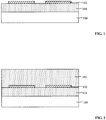
- Figure 1 shows a schematic view of a corresponding semiconductor substrate.
- a first substrate 100 is provided.
- a first dielectric layer 101 may be formed on the first substrate 100.
- a plurality of discrete first electrodes 102 may be formed on the first dielectric layer 101.
- the first substrate 100 may be used as a carrier substrate for subsequent fabrication process.
- the first substrate 100 may be made of Si, Ge, GeSi, SiC, or any other appropriate material, such as Group III-V compounds including GaAs, etc.
- the first dielectric layer 101 may be made of SiO x , SiN x , or any other appropriate dielectric material.
- the plurality of first electrodes 102 may be used as connection points to electrically connect subsequently-formed capacitors to other electronic components. Further, during a subsequent process to form a plurality of first sub-electrode material layers, the first electrodes 102 may also be used to electrically connect to the plurality of first sub-electrode material layers and thus form a plurality of parallel capacitors.
- the plurality of first electrodes 102 may be made of doped polycrystalline silicon or metal. In one embodiment, the plurality of first electrodes 102 are made of doped polycrystalline silicon.
- the plurality of first electrodes 102 may be formed by a process including the following steps. First, an electrode material layer may be formed on the first dielectric layer 101. Then, a plurality of discrete first electrodes 102 may be formed by etching the electrode material layer using an etch mask.
- a second dielectric layer may be formed to cover the plurality of first electrodes and the first dielectric layer (S102).
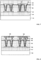
- Figure 2 shows a schematic cross-section view of the corresponding semiconductor structure.
- a second dielectric layer 103 may be formed on the plurality of first electrodes 102.
- the second dielectric layer 103 may cover the plurality of first electrodes 102 and the first dielectric layer 101.
- a plurality of capacitors may be formed in the second dielectric layer 103.
- the second dielectric layer 103 may be made of SiO x , SiN x , or any other appropriate dielectric material.
- a plurality of etched trenches may be formed in the second dielectric layer (S103).
- Figure 3 shows a schematic cross-section view of the corresponding semiconductor structure.
- a plurality of etched trenches 104 may be formed in the second dielectric layer 103 by etching the second dielectric layer 103 using an etch mask. Each etched trench 104 may expose one or more portions of the surface of a corresponding first electrode 102.
- the plurality of etched trenches 104 may be used to form a plurality of capacitors in a subsequent process. Fabricating the plurality of capacitors based on the etched trenches 104 may ensure that the formed capacitors are relatively narrow along a lateral direction, i.e., along a direction parallel to the surface of the first substrate 100. In the meantime, the etched trenches 104 may also be able to improve the capacitance values of the formed capacitors despite the relatively narrow lateral spaces occupied by the capacitors.
- each etched trench 104 may include at least one sub-trench.
- each etched trench 104 when the number of sub-trenches in each etched trench 104 is greater than one, neighboring sub-trenches in each etched trench may be separated from each other and the bottoms of the sub-trenches may expose different portions of the surface of a same first electrode 102.
- each etched trench includes multiple sub-trenches, a capacitor may be formed in each sub-trench.
- the multiple capacitors formed in the sub-trenches of an etched trench may be electrically connected to a corresponding first electrode 102 and a corresponding second electrode formed subsequently. As such, the capacitance value between the two connection points, i.e. the first electrode 102 and the subsequently-formed second electrode, may be further improved.
- an increase in the capacitance value may be helpful for reducing thermal noise generated during the operation of the CMOS image sensor.
- an increase in the capacitance value may help to reduce kTC noise, which is known as a fluctuation noise of a resistor in a charging circuit due to temperature fluctuation during charging-and-discharging process.
- each etched trench 104 having two sub-trenches 104a the shapes and the dimensions of the sub-trenches 104a may be the same so that the subsequently-formed capacitors in the sub-trenches may be identical in shape, structure, and electrical properties. Therefore, in addition to the increased total capacitance value, the capacitors formed in the sub-trenches 104a may have highly consistent charging-and-discharging properties, which may further improve the performance of the CMOS image sensor.
- the afore-mentioned shape of the sub-trenches 104a may refer to the cross-section shape of each sub-trench 104a along a direction perpendicular to the surface of the first substrate 100 and the cross-section shape of each sub-trench 104a along a direction parallel to the surface of the first substrate 100.
- the cross section of each sub-trench 104a along a direction perpendicular to the surface of the first substrate 100 may have a V-shape or a U-shape; while the cross section of each sub-trench 104a along a direction parallel to the surface of the first substrate 100 may have a circular shape, a polygonal shape, or any other appropriate shape.
- the dimensions of the sub-trenches 104a may refer to the depth and/or the width of the sub-trenches 104a.
- each sub-trench 104a has a V-shaped cross section along a direction perpendicular to the surface of the first substrate 100.
- the extension line of the sidewall of each sub-trench 104a and the surface of the first substrate 100 may form an angle in a range of 60° to 90°. Therefore, the upper opening width of each sub-trench 104a may be relatively large and the opening width may gradually decrease as moving towards the bottom of the sub-trench 104a. Therefore, in a subsequent process to form the first electrode material layer, the deposition material may not accumulate at the upper opening of each sub-trench 104a; instead, the deposition material may also be uniformly formed on the sidewall surface of the sub-trench 104a towards the bottom of the sub-trench 104a.
- a first electrode material layer with a uniform thickness may be formed on the bottom and the sidewall surfaces of each sub-trench 104a. Further, the V-shaped sub-trenches 104a may also ensure a uniformly distributed dielectric material layer to be formed in a subsequent deposition process.
- each sub-trench 104a along a direction parallel to the surface of the first substrate 100 may have a circular shape, thus the sidewall surfaces of the sub-trenches 104a may not have sharp turning corners. Therefore, the circular shape may be helpful for improving thickness uniformity of the first electrode material layer formed on the sidewall surfaces of the sub-trenches 104a. Further, after filling a second electrode material layer on the surface of the dielectric material layer formed in the sub-trenches 104a, the distance between the V-shaped first electrode material layer and the second electrode material layer may be uniform and the dielectric constant of the dielectric material layer may also be uniform. Therefore, the precision of the capacitance value of the formed capacitors may be improved.
- the V-shaped sub-trenches 104a may be formed by a plasma etching process.
- the plasma etching process may use an etching gas including CF 4 , CHF 3 , and Ar.
- the flow rate of CF 4 may be in a range of 10 sccm to 200 sccm
- the flow rate of CHF 3 may be in a range of 10 sccm to 200 sccm
- the flow rate of Ar may be in a range of 50 sccm to 200 sccm.
- the process parameters used in the plasma etching process may also include a source power in a range of 1100 W to 1250 W, an offset power in a range of 200 W to 220 W, an etching chamber pressure in a range of 10 mTorr to 20 mTorr, and an etching chamber temperature in a range of 20 °C to 100 °C.
- a source power in a range of 1100 W to 1250 W
- an offset power in a range of 200 W to 220 W
- an etching chamber pressure in a range of 10 mTorr to 20 mTorr
- an etching chamber temperature in a range of 20 °C to 100 °C.
- each sub-trench 104a along the direction perpendicular to the surface of the first substrate 100 may have a U shape, a rectangular shape, or any other appropriate shape.
- each sub-trench 104a along the direction parallel to the surface of the first substrate 100 may have a polygon shape or any other appropriate shape.
- a first electrode material layer may be formed on the sidewall and the bottom surfaces of each etched trench (S104).
- Figure 4 shows a schematic cross-section view of the corresponding semiconductor structure.
- a plurality of first electrode material layers 105 may be formed on the sidewall and the bottom surfaces of the etched trenches 104. Specifically, the sidewall surface and the bottom surface of each sub-trench 104a may be covered by a corresponding first electrode material layer 105. Each first electrode material layer 105 may be used as an electrode of a subsequently-formed capacitor.
- the plurality of first electrode material layers 105 are made of doped polycrystalline silicon. Using a deposition process to form doped polycrystalline silicon on the sidewall and the bottom surfaces of the sub-trenches 104a may ensure a desired uniformity for the formed first electrode material layer 105. In addition, the stress between the first electrode material layers 105 and the second dielectric layers 103 may be small, thus the properties of subsequently-formed capacitors may be improved.
- the doping ions in the doped polycrystalline silicon may be phosphor ions, arsenic ions, or boron ions.
- the concentration of the doping ions in the first electrode material layers 105 may not be too small; otherwise, the subsequently-formed capacitors may have relatively large parasitic resistance, thus the time required to charge or discharge the capacitors may be long, and the signal transfer in the CMOS image sensor may be significantly affected.
- the thickness of the first electrode material layers 105 may not be too small or too large. Specifically, when the first electrode material layers 105 is too thin, parasitic resistance may become very large; however, when the first electrode material layers 105 is too thick, the capacitance value of the subsequently-formed capacitors may be affected.
- the concentration of the doping ions in the first electrode material layer 105 may be in a range of 1E17 atom/cm 3 to 1E21 atom/cm 3 and the thickness of the first electrode material layer 105 may be in a range of 200 ⁇ to 1000 ⁇ .
- the first electrode material layer 105 may be formed by a process including the following steps. First, a first electrode material layer may be formed by a chemical vapor deposition (CVD) process to cover the second dielectric layer 103 and the sidewall and the bottom surfaces of the etched trenches 104. Then, a chemical mechanical polishing (CMP) process or an etch-back process may be performed to remove the portion of the first electrode material layer formed on the surface of the second dielectric layer 103. As such, the remaining portion of the first electrode material layer formed inside of the etched trenches 104 may then form the plurality of first electrode material layers 105.
- CVD chemical vapor deposition
- CMP chemical mechanical polishing
- etch-back process an etch-back process
- a sacrificial layer may be formed on the surface of the first electrode material layer in each etched trench 104 to fill up the etched trench 104 prior to performing the CMP process or the etch-back process in order to ensure that the first electrode material layer formed in each etched trench 104 will not be affected by the CMP process or the etch-back process.
- the sacrificial layer may be removed so that the surface of the portion of the first electrode material layer formed in each etched trench 104 is exposed.
- the sacrificial layer may be made of photoresist or any other appropriate sacrificial material.
- the CVD process to form the first electrode material layer may use a silicon-containing gas such as SiH 4 and SiH 2 Cl 2 .
- the process parameters used in the CVD process may include a flow rate of the silicon-containing gas in a range of 10 sccm to 300 sccm, a reaction temperature in a range of 500 °C to 800°C, and a reaction pressure in a range of 10 mTorr to 100 mTorr.
- the CVD process may also use H 2 as a carrier gas and the flow rate of H 2 may be in a range of 0.1 slm to 40 slm. Using the process parameters described above may improve the uniformity of the formed first electrode material layers 105.
- the doping ions in the first electrode material layers 105 may be formed by an in-situ method during the deposition process or by an ion implantation process performed after the completion of the deposition process.
- a first sub-electrode material layer may be formed in each sub-trench 104a of the etched trench 104.
- the first sub-electrode material layers formed in neighboring sub-trenches may be separated from each other.
- the multiple first sub-electrode material layers formed in sub-trenches of an etched trench 104 may together form a first electrode material layer.
- the bottoms of the multiple first sub-electrode material layers of the etched trench 104 may all electrically connect to a corresponding first electrode 102.
- each trench 104 includes two sub-trenches.
- a first sub-electrode material layer 105a may be formed in each sub-trench. Two first sub-electrode material layers 105a together form a first electrode material layer 105.
- a dielectric material layer may be formed on the surface of the first electrode material layers and the surface of the second dielectric layer
- FIG. 5 shows a schematic cross-section view of the corresponding semiconductor structure.
- a dielectric material layer 106 is formed on the surfaces of the plurality of first electrode material layers 105 and the second dielectric layer 103.
- the portion of the dielectric material layer 106 formed in the etched trenches may be used to define the capacitance values for the subsequently-formed capacitors; while the portion of the dielectric material layer 106 formed on the surface of the second dielectric layer 103 may be used as an isolation layer to separate subsequently-formed second electrodes from first electrode material layers 105.
- the dielectric material layer 106 may be made of one or more of SiO x , SiN x , SiON, and high-k dielectric material.
- the high-k dielectric material may include HfO 2 , TiO 2 , HfZrO, HfSiNO, Ta 2 O 5 , ZrO 2 , ZrSiO 2 , Al 2 O 3 , SrTiO 3 , BaSrTiO, etc.
- the dielectric material layer 106 may be formed by atomic layer deposition (ALD), plasma enhanced chemical vapor deposition (PECVD), secondary pressure chemical vapor deposition, or sputtering.
- ALD atomic layer deposition
- PECVD plasma enhanced chemical vapor deposition
- secondary pressure chemical vapor deposition secondary pressure chemical vapor deposition
- sputtering secondary pressure chemical vapor deposition
- the dielectric material layer 106 may also be formed by any other appropriate process.
- the dielectric material layer 106 may be formed by ALD.
- the thickness of the dielectric material layer 106 may be in a range of 10 ⁇ to 500 ⁇ .
- a plurality of discrete second electrode material layers and a plurality of discrete second electrodes may be formed on the surface of the dielectric material layer (S106).
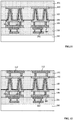
- Figure 6 shows a schematic cross-section view of the corresponding semiconductor structure.
- a second electrode material layer 107 may be formed on the surface of the portion of the dielectric material layer 106 formed in each etched trench 104 (referring to Figure 5 ). Each second electrode material layer 107 may fill up the remaining portion of the corresponding etched trench 104. Further, a second electrode 110 may be formed on the dielectric material layer 106 corresponding to each etched trench 104. The second electrode 110 may be electrically connected to the corresponding second electrode material layer 107. Moreover, neighboring second electrodes 110 may be separated from each other.
- the plurality of second electrode material layers 107 and the plurality of second electrodes 110 may be made of doped polycrystalline silicon.
- the doping type of the second electrode material layers 107 as well as the doping type of the second electrodes 110 may be the same as the doping type of the first electrode material layers 102.
- dashed lines in Figure 6 are used to schematically separate each second electrode 110 from the corresponding second electrode material layer 107.
- Each second electrode material layer 107 may be used as an electrode for a subsequently-formed capacitor, while a corresponding first electrode material layer 105 may be used as another electrode for the subsequently-formed capacitor.
- the plurality of second electrodes 110 may be used as connection points to further connect the plurality of formed capacitors to other electronic components.
- the second electrode 110 may electrically connect the multiple discrete second sub-electrode material layers formed in the sub-trenches 104a (referring to Figure 5 ) of a corresponding etched trench 104. Therefore, a plurality of parallel capacitors may be formed between each second electrode 110 and a corresponding first electrode 102. As such, the capacitance value of the capacitor formed between a second electrode 110 and a corresponding first electrode 102 may be increased, thus kTC noise generated during the operation of the CMOS image sensor may be reduced.
- each first electrode 102 may be electrically connected to an output terminal of a corresponding image sensing unit formed on a third substrate while each second electrode 110 may be electrically connected to a terminal of a signal processing circuit formed on a second substrate.
- the capacitor formed between a first electrode 102 and a second electrode 110 may be used to store induced charges coming out from the image sensing unit so that sharp images may be obtained when capturing images of moving objects.
- the CMOS image sensor formed in the present invention may be used in global shutter camera, camcorder, or other imaging equipment. When camera, camcorder, or other imaging equipment adopting the CMOS image sensor formed by the disclosed method is used to capture images of moving objects, the obtained images may not be deformed.
- the plurality of second electrodes 110 and the plurality of second electrode material layers 107 may be formed simultaneously.
- the process to simultaneously form the second electrodes 110 and the second electrode material layers 107 may include the following steps. First, a doped polycrystalline silicon layer may be formed to cover the dielectric material layer 106. The doped polycrystalline silicon layer may also fill up the plurality of etched trenches. Further, a planarization process (such as CMP process) may be performed to planarize the surface of the doped polycrystalline silicon layer. A mask layer may then be formed on the doped polycrystalline silicon layer after the planarization process. The mask layer may cover a portion of the polycrystalline silicon layer formed on each etched trench 104 (referring to Figure 5 ).
- the portion of the doped polycrystalline silicon layer exposed by the mask layer may be removed by an etching process using the mask layer as an etch mask.
- a plurality of discrete second electrode material layers 107 may then be formed on the dielectric material layer 106 in the plurality of etched trenches.
- the plurality of second electrode material layers 107 may fill up the plurality of etched trenches.
- a second electrode 110 may be simultaneously formed on the surface of a corresponding second electrode material layer 107.
- a second sub-electrode material layer may be formed on the dielectric material layer in each sub-trench. That is, multiple second sub-electrode material layers may be formed in each etched trench. Further, neighboring second sub-electrode material layers may be separated from each other. The multiple second sub-electrode material layers together may form a second electrode material layer corresponding to the etched trench. Moreover, the multiple second sub-electrode material layers formed in a corresponding etched trench may be electrically connected with each other through a second electrode.
- the number of the sub-trenches in each etched trench is two.
- a second sub-electrode material layer 107a may be formed on the dielectric material layer 106 in each sub-trench.
- a second electrode material layer 107 may be formed by two second sub-electrode material layers 107a. Further, the two second sub-electrode material layers 107a may be electrically connected with each other through a second electrode 110.
- a third dielectric layer may be formed to cover the plurality of second electrodes and the dielectric material layer (S107).
- Figure 7 shows a schematic cross-section view of the corresponding semiconductor structure.
- a third dielectric layer 108 may be formed on the plurality of second electrodes 110 and the dielectric material layer 106.
- the third dielectric layer 108 may be made of SiO x , SiN x , or any other appropriate dielectric material.
- the third dielectric layer 108 may have a single-level structure or a multiple-level ( ⁇ 2 levels) stacked structure.
- a plurality of first metal interconnections may be formed in the third dielectric layer with each first metal interconnection electrically connected to a corresponding second electrode (S108).
- Figure 8 shows a schematic cross-section view of the corresponding semiconductor structure.
- a plurality of first metal interconnections 109 may be formed in the third dielectric layer 109. Each first metal interconnection 109 may be electrically connected to a corresponding second electrode 110.
- the plurality of first metal interconnections 109 may be used as electrical leads to connect the connection points on the plurality of second electrodes 110. Moreover, the plurality of first metal interconnections 109 may be bonded to a plurality of second metal interconnections formed on a second substrate in a subsequent metal bonding process, thus the bonding strength and the mechanical stability of the image sensor may both be improved.
- the first metal interconnections may also be used as a light-shielding layer to prevent incident light from affecting the signal processing circuit on the second substrate.
- the signal processing circuit on the second substrate may include a plurality of transistors and the transistors may include a plurality of doped regions such as source/drain regions formed in the second substrate. When the doped regions are exposed to light, induced charges may be generated, thus the performance of the transistor may be affected.
- the plurality of first metal interconnections may serve as a light-shielding layer to prevent creating induced charges, thus the performance of the signal processing circuit may be improved.
- the plurality of first metal interconnections 109 may be made of Cu, W, Al, or any other appropriate conductive metal or their alloy(s).
- the plurality of first metal interconnections 109 may have a double-Damascus interconnection structure or a single-Damascus interconnection structure.
- the first metal interconnection 109 may be formed by a process including the following steps. First, a portion of the third dielectric layer 108 may be removed by etching. Specifically, a plurality of trenches may be formed in the third dielectric layer 108 after etching. Each trench may correspond to a second electrode 110 and may be formed above the corresponding second electrode 110. Further, at least two etched vias may be formed in the third dielectric layer 108 by removing a portion of the third dielectric layer 108 on the bottom of each trench.
- the surface of the corresponding second electrode 110 may be exposed on the bottom of each etched vias.
- the etched vias and the corresponding trench may be interconnected with each other.
- the trenches and the etched vias may be filled with metal to form a plurality of first metal interconnections 109.
- the surface of the plurality of first metal interconnections 109 may be leveled with the surface of the third dielectric layer 108.
- each first metal interconnection may also be formed by a metal layer and multiple metal plugs with the multiple metal plugs connecting with the metal layer.
- the metal layer may have a multiple-level structure and neighboring levels of the metal layer may be electrically connected with each other through metal plugs.
- a second substrate may be provided (S201).
- Figure 9 shows a schematic view of the second substrate.
- a second substrate 200 is provided.
- a plurality of discrete signal processing circuits 205 may be formed on the second substrate 200.
- a fourth dielectric layer 201 may be formed to cover the second substrate 200.
- a plurality of discrete second metal interconnections 202 may be formed in the fourth dielectric layer 201 with each second metal interconnection 202 electrically connected to a corresponding signal processing circuit 205.
- the plurality of signal processing circuits may be used to process electrical signals generated by image sensing units formed on a third substrate.
- the plurality of signal processing circuits may be formed on the second substrate 200 by an integrated process.
- the signal processing circuits may be integrated circuits including a plurality of semiconductor devices and a plurality of interconnections connecting the plurality of semiconductor devices.
- the semiconductor devices may include active devices (such as transistors, etc.) and/or passive devices (such as resistors, capacitors, etc.).
- the interconnections may include metal plugs and metal lines electrically connecting with the metal plugs.
- the second substrate 200 may be a semiconductor substrate with a dielectric layer formed on the semiconductor substrate.
- the semiconductor substrate may be made of Si, GeSi, silicon on insulator (SOI), or any other appropriate semiconductor material.
- a plurality of active devices may be formed on the semiconductor substrate.
- the dielectric layer may have a single-level structure or a multiple-level stacked structure.
- a plurality of interconnections and a plurality of passive devices may be formed in the dielectric layer.
- the fourth dielectric layer 201 may cover the second substrate 200.
- the fourth dielectric layer 201 may be made of SiO x , SiN x , or any other appropriate dielectric material.
- the fourth dielectric 201 may be formed on the second substrate 200 through a CVD process.
- the surface of the second metal interconnections 202 may be leveled with the surface of the fourth dielectric layer 201.
- the number of the second metal interconnections 202 may be multiple and each second metal interconnection 202 may be electrically connected with a corresponding signal process circuit.
- the plurality of second metal interconnections 202 may be used as connection terminals for the signal processing circuits to further connect to the corresponding capacitors formed on the first substrate 100. Further, the plurality of second metal interconnections 202 and the plurality of first metal interconnections 109 (referring to Figure 8 ) may be bonded together through a metal bonding process to improve the bonding strength between different layers and the mechanical stability of the formed CMOS image sensor.
- the plurality of second metal interconnections 202 may have a double-Damascus interconnection structure or a single-Damascus interconnection structure.
- each second metal interconnections may be an interconnection formed by a metal line and multiple metal plugs with the multiple metal plugs electrically connected with each other through the metal line.
- Figure 10 shows a schematic cross-section view of the corresponding semiconductor structure.
- the third dielectric layer 108 and the fourth dielectric layer 201 may be bonded together through a fusion bonding process. Specifically, the plurality of first metal interconnections 109 formed in the third dielectric layer 108 may be bonded to the plurality of second metal interconnections 202 formed in the fourth dielectric layer 201 so that each first metal interconnection 109 may be electrically connected to a corresponding second metal interconnection 202.
- the third dielectric layer 108 and the fourth dielectric layer 201 may be bonded with each other through a fusion bonding process.
- the plurality of first metal interconnections and the plurality of second metal interconnections 202 may be bonded together through a metal bonding process.
- the bonding strength and the mechanical stability of the bonding interface may be improved.
- the fusion bonding process may be performed before performing the metal bonding process.
- the bonding temperature may be in a range of 350 °C to 450 °C.
- the first substrate may be removed (S203).
- Figure 11 shows a schematic cross-section view of the corresponding semiconductor structure.
- the first substrate 100 may be removed.
- the semiconductor structure shown in Figure 11 is a structure flipped from the structure shown in Figure 10 with the first substrate 100 removed.
- a plurality of third metal interconnections may be formed in the first dielectric layer (S204).
- Figure 12 shows a schematic cross-section view of the corresponding semiconductor structure.
- a plurality of third metal interconnections 112 may be formed in the first dielectric layer 101.
- the plurality of third metal interconnections 112 may be electrically connected to the plurality of first electrodes 102.
- the plurality of third metal interconnections 112 may serve as electrical leads to connect the connection points on the plurality of first electrodes 102.
- the plurality of third metal interconnections 112 may be bonded to a plurality of fourth metal interconnections formed on a third substrate in a subsequent metal bonding process (that is, the output terminal of each image sensing unit may be electrically connected to an electrode of a corresponding capacitor so that the capacitor can store photo-generated charges from the image sensing unit) in order to improve the bonding strength at the bonding interface.
- the third metal interconnections 112 may also be used as a light-shielding layer to prevent undesired effects (such as causing induced charges in the doped silicon) due to downward transfer (e.g. along a direction toward capacitors and signal processing circuits) of external light. Such undesired influence may further affect the performance of capacitors and signal processing circuits.
- the plurality of third metal interconnections 112 may have a double-Damascus interconnection structure or a single-Damascus interconnection structure.
- each third metal interconnection may be formed by a metal layer and a metal plug with the metal plug electrically connected with the metal layer.
- a third substrate may be provided (S301).
- Figure 13 shows a schematic view of the corresponding semiconductor structures.
- a third substrate 300 may be provided and a plurality of discrete image sensing units 303 may be formed on the third substrate 300.
- Each image sensing unit may be a pixel of the image sensor.
- Each image sensing unit may include a photodiode and a plurality of transistors.
- the photodiode may be used for sensing external light and creating photo-induced carriers.
- the plurality of transistors may be used to control the collection and transfer process for photo-induced carriers.
- each image sensing unit may include a photodiode and three or four transistors.
- the image sensing unit When an image sensing unit contains three transistors together with a photodiode, the image sensing unit is a 3T-type, while when an image sensing unit contains four transistors together with a photodiode, the image sensing unit is a 4T-type.
- the present invention is described to have a plurality of 4T-type image sensing units. In other embodiments, the image sensing units may be 3-T type or any other appropriate type.
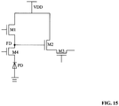
- each 4T-type image sensing unit may include four MOS transistors and one photoelectric diode PD.
- the four MOS transistors may be a reset transistor M1, an amplifier transistor M2, a selection transistor M3, and a transfer transistor M4.
- the operation procedure of the pixel unit in the 4T-type image transistor shown in Figure 15 may include the following steps. First, prior to receiving light illumination, the reset transistor M1 and the transfer transistor M4 may be turned on while the other transistors may be turned off so that the floated diffusion FD region and the photodiode PD may be reset. Then, all transistors may be turned off and the photodiode PD may receive illumination of light. Further, photo-induced carriers may then be generated through the photoelectrical conversion process. With the transfer transistor M4 turned on while the other transistors all turned off, the photo-induced carriers may then be transferred to the floated diffusion FD region. Further, the amplifier transistor M2 and the selection transistor M3 may be turned on. By sequentially passing through the floated diffusion FD region, the amplifier transistor M2, and the selection transistor M3, photo-induced carriers may be sent out, thus one collection and transfer of optical signal may be completed.
- the image sensing units 303 may be formed by an existing semiconductor integrated manufacturing process. One may refer to existing fabrication methods for the details of the manufacturing process.
- the formed image sensing units 303 may be back side illumination (BSI) type image sensing units. That is, external light may be irradiated from the back side of the third substrate 300 (referring to Figure 13 ).
- BSI back side illumination
- transistors as well as interconnections connecting the transistors may be formed on the front side of the third substrate 300 to improve the integration degree of the formed image sensing units 303.
- a fifth dielectric layer 301 may also be formed on the third substrate 300.
- a plurality of discrete fourth metal interconnections 304 may be formed in the fifth dielectric layer 301.
- the plurality of fourth metal interconnections 304 may be electrically connected to the output terminals of the plurality of image sensing units 303.
- the surface of the fourth metal interconnections 304 may be leveled with the surface of the fifth dielectric layer 301.
- the plurality of fourth metal interconnections 304 may have a double-Damascus interconnection structure or a single-Damascus interconnection structure.
- each fourth metal interconnection may be formed by a metal layer and a metal plug with the metal plug electrically connected with the metal layer.
- each fourth metal interconnection 304 may be electrically connected to a corresponding image sensing unit 303. In other embodiments, each fourth metal interconnection may be electrically connected to at least two image sensing units.
- Figure 14 shows a schematic cross-section view of the corresponding semiconductor structure.
- the first dielectric layer 101 may be bonded to the fifth dielectric layer 301.
- the plurality of third metal interconnections 112 in the first dielectric layer 101 may be bonded to the plurality of fourth metal interconnections 304 in the first dielectric layer so that each third metal interconnection 112 may be electrically connected to a corresponding fourth metal interconnection 304.
- the first dielectric layer 101 and the fifth dielectric layer 301 may be bonded together through a fusion bonding process.
- the third metal interconnections 112 and the fourth metal interconnections 304 may be bonded with each other through a metal bonding process.
- the bonding strength and the mechanical stability at the bonding interface may be improved.
- the fusion bonding process may be performed before performing the metal bonding process.
- the bonding temperature may be in a range of 350 °C to 450 °C.
- a bottom signal processing layer including signal processing circuits
- an intermediate capacitor layer including capacitors
- an image sensor layer including image sensing units
- the bottom signal processing layer, the intermediate capacitor layer, and the image sensor layer may then be bonded together to form a stacked structure with electrical connections between the image sensor layer and the intermediate capacitor layer and also between the intermediate capacitor layer and the signal processing layer.
- the signal processing circuits and the capacitors may be formed on substrates different from the substrate on which image sensing units are formed. Therefore, while a relatively high integration degree of CMOS image sensors is still ensured, the photosensitive areas of the image sensing units formed on the third substrate may be made larger so that the fill factor of the CMOS image sensor may be improved.
- the first electrode material layers for the capacitors in the intermediate capacitor layer may be formed on the sidewall and the bottom surfaces of the etched trenches so that the first electrode material layers may have a reversed V-shape or a reversed U-shape. Therefore, the area of the first electrode material layer may be increased and the capacitance value of the formed capacitors may also be improved. As a result, thermal noise (kTC noise) generated during the operation of the CMOS image sensor may be reduced.
- kTC noise thermal noise
- the first metal interconnections, the second metal interconnections, the third metal interconnections, and the fourth metal interconnections may also be used to prevent undesired effects (e.g., causing induced charges in the doped silicon) due to downward transfer of external light (i.e., light transfer along a direction toward capacitors and signal processing circuits). Such undesired influence may further affect the performance of capacitors and signal processing circuits.
- the bonding strength and the mechanical stability at the bonding interface may be improved.
- the present invention also provides a CMOS image sensor.
- Figure 14 shows a schematic cross-section view of an exemplary CMOS image sensor consistent with disclosed embodiments.
- the disclosed CMOS image sensor may include a bottom signal processing layer.
- the bottom signal processing layer may further include a second substrate 200, a plurality of discrete signal processing circuits (not shown) formed on the second substrate 200, a fourth dielectric layer 201 formed on the second substrate 200, and a plurality of discrete second metal interconnections 202 formed in the fourth dielectric layer 201.
- Each second metal interconnection may be electrically connected to a corresponding signal processing circuit.
- the CMOS image sensor may also include an intermediate capacitor layer.
- the intermediate capacitor layer may include a dielectric layer and a plurality of capacitors formed in the dielectric layer. Each capacitor may further include a first electrode 102, a reversed V-shaped or U-shaped first electrode material layer 105 electrically connecting to the first electrode 102, a second electrode material layer 107 corresponding to the first electrode material layer 105, a second electrode 110 electrically connecting to the second electrode material layer 107, and a dielectric material layer 106 formed between the first electrode material layer 105 and the second electrode material layer 107.
- the intermediate capacitor layer may also include a third metal interconnection 112 formed in the dielectric layer and electrically connected with the first electrode 102. The third metal interconnection 112 may be formed above the first electrode 102.
- the intermediate capacitor layer may include a plurality of first metal interconnections 109 electrically connected with the plurality of second electrodes 110.
- Each first metal interconnection 109 may be situated below the corresponding second electrode 110. Further, each first metal interconnection 109 may be bonded to a corresponding second metal interconnection 202 in the bottom signal processing layer.
- the CMOS image sensor may further include an image sensor layer formed above the intermediate capacitor layer.
- the image sensor layer may include a third substrate 300, a plurality of discrete image sensing units 303 formed on the front side of the third substrate 300, a fifth dielectric layer 301 formed on the front side of the third substrate 300, and a plurality of discrete fourth metal interconnections 304 formed in the fifth dielectric layer 301.
- One terminal of each fourth metal interconnection 304 maybe electrically connected to an output terminal of a corresponding image sensing unit 303 while the other terminal of the fourth metal interconnection 304 may be bonded to a corresponding third metal interconnection 112 in the intermediate capacitor layer.
- the dielectric layer may include a third dielectric layer 108, a second dielectric layer 103 formed above the third dielectric layer 108, and a first dielectric layer 101 formed above the second dielectric layer 103.
- the first metal interconnections 109 and the second electrodes 110 may be formed in the third dielectric layer 108; the first electrodes 102, the first electrode material layers 105, a portion of the dielectric material layer 106, and the second electrode material layers 107 may be formed in the second dielectric layer 103; while the third metal interconnections 112 may be formed in the first dielectric layer 101.
- Each reversed V-shaped or U-shaped first electrode material layer 105 may include at least one reversed V-shaped or U-shaped first sub-electrode material layer.
- each reversed V-shaped or U-shaped first electrode material layer 105 includes two or more reversed V-shaped or U-shaped first sub-electrode material layers
- the bottoms of the reversed V-shaped or U-shaped first sub-electrode material layers may be connected with each other through a corresponding first electrode.
- the open ends of neighboring reversed V-shaped or U-shaped first sub-electrode material layers may be separated from each other.
- Each reversed V-shaped or U-shaped first sub-electrode material layer may correspond to a second sub-electrode material layer in the dielectric layer. Neighboring second sub-electrode material layer may be separated from each other.
- Each second sub-electrode material layer may be formed inside of the corresponding V-shaped or U-shaped first sub-electrode material layer.
- the first sub-electrode material layer and the corresponding second sub-electrode material layer may be isolated from each other by a dielectric material layer.
- a plurality of second sub-electrode material layers may form a second electrode material layer, and the plurality of second sub-electrode material layers may be electrically connected together with each other through a corresponding second electrode.
- each first electrode material layer is described to have a reversed V-shape and may include 2 reversed V-shaped sub-electrode material layers.
- the shape of the first electrode material layer may be U-shape or any other appropriate shape and the number of first sub-electrode material layers in each first electrode material layer may be more than two.
- the two reversed V-shaped sub-electrode material layers may be electrically connected with each other through a corresponding first electrode 102. The open ends of the two reversed V-shaped sub-electrode material layers may be separated from each other.
- Each reversed V-shaped first sub-electrode material layer may correspond to a second sub-electrode material layer in the dielectric layer.
- the two second sub-electrode material layers may also be separated from each other. Each second sub-electrode material layer may be formed inside of the corresponding V-shaped first sub-electrode material layer. The first sub-electrode material layer and the corresponding second sub-electrode material layer may be isolated from each other by a dielectric material layer 106. The two second sub-electrode material layers may form a second electrode material layer, and the two second sub-electrode material layers may be electrically connected with each other through a corresponding second electrode 110.
- the plurality of second metal interconnections 202 and the plurality of first metal interconnections 109 may be bonded together through a metal bonding process.
- the fourth metal interconnections 304 and the third metal interconnections 112 may be bonded with each other through a metal bonding process.
- the dielectric layer and the fifth dielectric layer 301 may be bonded together through a fusion bonding process.
- the plurality of first electrode material layers may also have any other appropriate concave shape.
- the plurality of first electrodes 102 and the plurality of second electrodes 110 may be made of doped polycrystalline silicon or metal.
- the plurality of first electrode material layers 105 and the plurality of second electrode material layers 110 may be made of doped polycrystalline silicon.
- the thickness of the plurality of first electrode material layers 105 may be in a range of 200 ⁇ to 1000 ⁇ .
- the concentration of the doping ions in the plurality of first electrode material layers 105 may be in a range of 1E17 atom/cm 3 to 1E21 atom/cm 3 .
- the disclosed CMOS image sensor with a stacked structure and fabrication methods may demonstrate the following advantages.
- a bottom signal processing layer including signal processing circuits
- an intermediate capacitor layer including capacitors
- an image sensor layer including image sensing units
- the bottom signal processing layer, the intermediate capacitor layer, and the image sensor layer may then be bonded together to form a stacked structure with electrical connections between the image sensor layer and the intermediate capacitor layer and also between the intermediate capacitor layer and the signal processing layer.
- the signal processing circuits and the capacitors may be formed on substrates different from the substrate on which image sensing units are formed. Therefore, while a relatively high integration degree of CMOS image sensors is still ensured, the photosensitive areas of the image sensing units formed on the third substrate may be made larger so that the fill factor of the CMOS image sensor may be improved.
- the first electrode material layers of the capacitors in the intermediate capacitor layer may be formed on the sidewall and the bottom surfaces of the etched trenches, thus the area of the first electrode material layer may be increased and the capacitance value of the formed capacitors may also be improved. As a result, thermal noise (kTC noise) generated during the operation of the CMOS image sensor may be reduced.
- the first metal interconnections, the second metal interconnections, the third metal interconnections, and the fourth metal interconnections may also be used to prevent undesired effects (e.g., causing induced charges in the doped silicon) due to downward transfer of external light (i.e., light transfer along a direction toward capacitors and signal processing circuits). Such undesired influence may further affect the performance of capacitors and signal processing circuits.
- the bonding strength and the mechanical stability at the bonding interface may be improved.
- each etched trench 104 when the number of sub-trenches in each etched trench 104 is greater than one, neighboring sub-trenches in each etched trench may be separated from each other and the bottoms of the sub-trenches may expose different portions of the surface of a same first electrode 102.
- a capacitor may be formed in each sub-trench.
- the multiple capacitors formed in the multiple sub-trenches may be electrically connected with a corresponding first electrode 102 and a corresponding second electrode 110. As such, the capacitance value between the connection points, i.e. the first electrode 102 and the second electrode 110, may further increase, which may be helpful for reducing thermal noise, i.e.
- kTC noise which is generated during the operation of CMOS image sensor. Specifically, as a fluctuation noise of the resistor in the charging-and-discharging circuit due to temperature fluctuation during charging-and-discharging process, kTC noise may be reduced.
Landscapes
- Solid State Image Pick-Up Elements (AREA)
- Engineering & Computer Science (AREA)
- Power Engineering (AREA)
Abstract
Description
- This application claims the priority of Chinese Patent Application No.
CN201510916698.6, filed on December 10,2015 - The present invention generally relates to the field of image sensing technology and, more particularly, relates to a stacked CMOS image sensor and fabrication methods thereof.
- With fast development of electrical and electronical technology, more and more modem mobile electronic products that use image sensor technology, such as smart phones, digital cameras, notebook computers, etc., have been rapidly developed and widely used. Currently, people spend significantly increased time on mobile phones and other electronic products and, tend to have more and more demands on product quality and personal experience. Today, most electronic devices are capable for snapping pictures and taking videos, and the total number of pixels in a camera has increased from the original several hundreds of thousands to five millions or even more. In electronic products, a major component for imaging is image sensor. Therefore, requirements on imaging quality of image sensors have become increasingly high.
- Image sensor is a device to convert optical signals into electrical signals. Image sensor includes charge coupled device (CCD) and complementary metal-oxide-semiconductor (CMOS) image transistor chip. Compared to traditional CCD sensor, CMOS image sensor demonstrates a number of advantages, such as low energy consumption, low cost, compatibility with CMOS technology, etc. Therefore, CMOS image sensor has become more popular. Specifically, CMOS image sensor has not only been used in the field of consumer electronics such as digital camera, cell phone camera, and camcorder, but also been widely used in the fields of automobile electronics, monitoring, biotechnology, and medical science, etc.
- However, CMOS image sensors fabricated by existing methods may need to be further improved. Specifically, the fill factor in existing CMOS image sensors may be relatively small and noise (such as kTC thermal noise) may be generated during the operation of the CMOS image sensors.
- The disclosed fabrication method and semiconductor structure are directed to solve one or more problems set forth above and other problems in the art.
- A first aspect of the present invention includes a method for fabricating a stacked CMOS image sensor. The method includes forming a first dielectric layer on a first substrate, forming a plurality of discrete first electrodes on the first dielectric layer, forming a second dielectric layer to cover the first dielectric layer and the plurality of first electrodes, forming a plurality of etched trenches in the second dielectric layer with each etched trench exposing one or more surface portions of a corresponding first electrode, forming a first electrode material layer on sidewall and bottom surfaces of each etched trench to electrically connect to a corresponding first electrode, forming a dielectric material layer to cover the second dielectric layer and the first electrode material layer in each etched trench, forming a second electrode material layer on the dielectric material layer to fill up each etched trench, and forming a plurality of discrete second electrodes with each second electrode electrically connecting to a corresponding second electrode material layer and also covering corresponding portions of the dielectric material layer. The method further includes forming a plurality of discrete signal processing circuits on a second substrate, and bonding the second substrate to the first substrate with each signal processing circuit electrically connected to a corresponding second electrode. Moreover, the method includes removing the first substrate to expose the first dielectric layer. Finally, the method includes forming a plurality of discrete image sensing units on a third substrate, and then bonding the third substrate to the exposed first dielectric layer with each image sensing unit electrically connected to a corresponding first electrode.
- Each etched trench may include one or more sub-trenches.
- The number of sub-trenches in each etched trench may be more than one.
- Preferably, neighboring sub-trenches are isolated from each other.
- Preferably, each sub-trench of an etched trench exposes a portion of a surface of a same first electrode.
- The method for fabricating the CMOS image sensor may further include: forming a first sub-electrode material layer on surfaces of a bottom and sidewalls of each sub-trench, wherein the dielectric material layer has a portion formed on the first sub-electrode material layer; and forming a second sub-electrode material layer on the dielectric material layer and within each sub-trench. Preferably, one first electrode material layer is formed by more than one first sub-electrode material layers corresponding to a same etched trench. Preferably, one second electrode material layer is formed by more than one second sub-electrode material layers corresponding to a same etched trench.
- Bonding the second substrate with the first substrate may further include: forming a fourth dielectric layer to cover the second substrate, wherein a plurality of discrete second metal interconnections are formed in the fourth dielectric layer and each second metal interconnection is electrically connected with a corresponding signal processing circuit; and bonding the third dielectric layer with the fourth dielectric layer with each first metal interconnection in the third dielectric layer bonded to a corresponding second metal interconnection in the fourth dielectric layer, wherein each first metal interconnect is electrically connected with the corresponding second metal interconnect.
- After removing the first substrate, a plurality of third metal interconnections may be formed in the first dielectric layer. Preferably, each third metal interconnection is electrically connected with a corresponding second electrode.
- Bonding the third substrate with the exposed first dielectric layer may further include: forming a fifth dielectric layer on the third substrate, wherein a plurality of discrete fourth metal interconnections are formed in the fifth dielectric layer and each fourth metal interconnection is electrically connected to a corresponding image sensing unit; and bonding the fifth dielectric layer with the exposed first dielectric layer with each third metal interconnection in the first dielectric layer bonded to a corresponding fourth metal interconnection in the fifth dielectric layer, wherein each third metal interconnect is electrically connected with the corresponding fourth metal interconnect.
- Bonding the second substrate with the first substrate and bonding the third substrate with the exposed first dielectric layer may include one or more of a fusion bonding process and a metal bonding process. Preferably, the fusion bonding process is performed before performing the metal bonding process. Preferably, the metal bonding process is performed at a temperature in a range of 350 °C to 450 °C.
- Preferably, the plurality of second electrode material layers and the plurality of first electrode material layers are made of doped polycrystalline silicon.
- Preferably, a thickness of the plurality of first electrode material layers is in a range of 200 Å to 1000Å.
- Preferably, a doping concentration in the plurality of first electrode material layers is in a range of 1E17 atom/cm3 to 1E21 atom/cm3.
- Preferably, the dielectric material layer is made of one or more of SiOx, SiNx, SiON, and a high-k dielectric material.
- Preferably, a thickness of the dielectric material layer is in a range of 10 Å to 500 Å.
- Preferably, the plurality of discrete second electrodes and the plurality of discrete first electrodes are made of doped polycrystalline silicon or a metal.
- Preferably, the plurality of first metal interconnections, the plurality of second metal interconnections, the plurality of third metal interconnections, and the plurality of fourth metal interconnections have a dual-Damascus interconnection structure or a single-Damascus interconnection structure.
- Preferably ,each fourth metal interconnection is electrically connected to one image sensing unit.
- Preferably, each fourth metal interconnection is electrically connected to at least two image sensing units.
- Preferably, the image sensing units are of the back side illumination (BSI) type.
- A second aspect of the present invention provides a stacked CMOS image sensor. The stacked CMOS image sensor includes a signal processing layer; an image sensor layer; and an intermediate capacitor layer between the signal processing layer and the image sensor layer. The signal processing layer includes a plurality of discrete signal processing circuits, the image sensor layer includes a plurality of discrete image sensing units each electrically connected to one first electrode of the intermediate capacitor layer, and the intermediate capacitor layer includes a dielectric layer, and a plurality of capacitors. Further, each capacitor includes a first electrode, a V-shaped or U-shaped first electrode material layer electrically connecting to the first electrode, a second electrode material layer on the first electrode material layer having the dielectric layer there-between, and a second electrode electrically connecting to the second electrode material layer and also to one signal processing circuit of the signal processing layer.
- Preferably, the CMOS image sensor further includes: A plurality of first metal interconnections formed in the intermediate capacitor layer with each first metal interconnection electrically connected to a corresponding second electrode; a plurality of second metal interconnections formed in the signal processing layer with each second metal interconnection electrically connected to a corresponding signal processing circuit; a plurality of third metal interconnections formed in the intermediate capacitor layer with each third metal interconnection electrically connected to a corresponding first electrode; and a plurality of fourth metal interconnections formed in the image sensor layer with each fourth metal interconnection electrically connected to a corresponding image sensing unit.
- Preferably, each first metal interconnection is bonded with a corresponding second metal interconnection to realize electrical connection between the corresponding signal processing circuit in the signal processing layer and the corresponding first electrode in the intermediate capacitor layer.
- Preferably, each third metal interconnection is bonded with a corresponding fourth metal interconnection to realize electrical connection between the corresponding second electrode in the intermediate capacitor layer and the corresponding image sensing unit in the image sensor layer.
- Preferably, each V-shaped or U shaped first electrode material layer includes one or more V-shaped or U-shaped first sub-electrode material layers.
- Preferably, each second electrode material layer, corresponding to a first electrode material layer, also includes one or more second sub-electrode material layers with each second sub-electrode material layer corresponding to a first sub-electrode material layer.
- Other aspects of the present invention can be understood by those skilled in the art in light of the description, the claims, and the drawings of the present invention.
- The following drawings are merely examples for illustrative purposes according to various disclosed embodiments and are not intended to limit the scope of the present invention.
-
Figures 1-14 illustrate schematic views of semiconductor structures corresponding to certain stages of an exemplary fabrication method for a CMOS image sensor consistent with disclosed embodiments; -
Figure 15 illustrates a structural diagram of a 4T-type image sensing unit in an exemplary CMOS image sensor consistent with disclosed embodiments; and -
Figure 16 illustrates a flowchart of an exemplary fabrication process consistent with disclosed embodiments. - Reference will now be made in detail to exemplary embodiments of the invention, which are illustrated in the accompanying drawings. Wherever possible, the same reference numbers will be used throughout the drawings to refer to the same or like parts.
-
Figure 16 shows a flowchart of an exemplary fabrication process for an exemplary CMOS image sensor consistent with disclosed embodiments.Figures 1-14 show schematic views of semiconductor structures corresponding to certain stages of the exemplary fabrication method. - In
Figure 16 , at the beginning of the fabrication process, a first substrate is provided (S101).Figure 1 shows a schematic view of a corresponding semiconductor substrate. - Referring to
Figure 1 , afirst substrate 100 is provided. Afirst dielectric layer 101 may be formed on thefirst substrate 100. A plurality of discretefirst electrodes 102 may be formed on thefirst dielectric layer 101. - The
first substrate 100 may be used as a carrier substrate for subsequent fabrication process. Thefirst substrate 100 may be made of Si, Ge, GeSi, SiC, or any other appropriate material, such as Group III-V compounds including GaAs, etc. - The
first dielectric layer 101 may be made of SiOx, SiNx, or any other appropriate dielectric material. - The plurality of
first electrodes 102 may be used as connection points to electrically connect subsequently-formed capacitors to other electronic components. Further, during a subsequent process to form a plurality of first sub-electrode material layers, thefirst electrodes 102 may also be used to electrically connect to the plurality of first sub-electrode material layers and thus form a plurality of parallel capacitors. - The plurality of
first electrodes 102 may be made of doped polycrystalline silicon or metal. In one embodiment, the plurality offirst electrodes 102 are made of doped polycrystalline silicon. - The plurality of
first electrodes 102 may be formed by a process including the following steps. First, an electrode material layer may be formed on thefirst dielectric layer 101. Then, a plurality of discretefirst electrodes 102 may be formed by etching the electrode material layer using an etch mask. - Further, returning to
Figure 16 , a second dielectric layer may be formed to cover the plurality of first electrodes and the first dielectric layer (S102).Figure 2 shows a schematic cross-section view of the corresponding semiconductor structure. - Referring to
Figure 2 , asecond dielectric layer 103 may be formed on the plurality offirst electrodes 102. Thesecond dielectric layer 103 may cover the plurality offirst electrodes 102 and thefirst dielectric layer 101. - In a subsequent process, a plurality of capacitors may be formed in the
second dielectric layer 103. Thesecond dielectric layer 103 may be made of SiOx, SiNx, or any other appropriate dielectric material. - Returning to
Figure 16 , further, a plurality of etched trenches may be formed in the second dielectric layer (S103).Figure 3 shows a schematic cross-section view of the corresponding semiconductor structure. - Referring to
Figure 3 , a plurality of etchedtrenches 104 may be formed in thesecond dielectric layer 103 by etching thesecond dielectric layer 103 using an etch mask. Eachetched trench 104 may expose one or more portions of the surface of a correspondingfirst electrode 102. - The plurality of etched
trenches 104 may be used to form a plurality of capacitors in a subsequent process. Fabricating the plurality of capacitors based on the etchedtrenches 104 may ensure that the formed capacitors are relatively narrow along a lateral direction, i.e., along a direction parallel to the surface of thefirst substrate 100. In the meantime, the etchedtrenches 104 may also be able to improve the capacitance values of the formed capacitors despite the relatively narrow lateral spaces occupied by the capacitors. - Further, each
etched trench 104 may include at least one sub-trench. - In one embodiment, when the number of sub-trenches in each
etched trench 104 is greater than one, neighboring sub-trenches in each etched trench may be separated from each other and the bottoms of the sub-trenches may expose different portions of the surface of a samefirst electrode 102. Further, when each etched trench includes multiple sub-trenches, a capacitor may be formed in each sub-trench. In addition, the multiple capacitors formed in the sub-trenches of an etched trench may be electrically connected to a correspondingfirst electrode 102 and a corresponding second electrode formed subsequently. As such, the capacitance value between the two connection points, i.e. thefirst electrode 102 and the subsequently-formed second electrode, may be further improved. Moreover, an increase in the capacitance value may be helpful for reducing thermal noise generated during the operation of the CMOS image sensor. For example, an increase in the capacitance value may help to reduce kTC noise, which is known as a fluctuation noise of a resistor in a charging circuit due to temperature fluctuation during charging-and-discharging process. - For illustration purpose, as shown in
Figure 3 , the present invention is primarily described based on eachetched trench 104 having two sub-trenches 104a. In one embodiment, the shapes and the dimensions of the sub-trenches 104a may be the same so that the subsequently-formed capacitors in the sub-trenches may be identical in shape, structure, and electrical properties. Therefore, in addition to the increased total capacitance value, the capacitors formed in the sub-trenches 104a may have highly consistent charging-and-discharging properties, which may further improve the performance of the CMOS image sensor. - The afore-mentioned shape of the sub-trenches 104a may refer to the cross-section shape of each sub-trench 104a along a direction perpendicular to the surface of the
first substrate 100 and the cross-section shape of each sub-trench 104a along a direction parallel to the surface of thefirst substrate 100. Specifically, the cross section of each sub-trench 104a along a direction perpendicular to the surface of thefirst substrate 100 may have a V-shape or a U-shape; while the cross section of each sub-trench 104a along a direction parallel to the surface of thefirst substrate 100 may have a circular shape, a polygonal shape, or any other appropriate shape. The dimensions of the sub-trenches 104a may refer to the depth and/or the width of the sub-trenches 104a. - In one embodiment, each sub-trench 104a has a V-shaped cross section along a direction perpendicular to the surface of the
first substrate 100. The extension line of the sidewall of each sub-trench 104a and the surface of thefirst substrate 100 may form an angle in a range of 60° to 90°. Therefore, the upper opening width of each sub-trench 104a may be relatively large and the opening width may gradually decrease as moving towards the bottom of the sub-trench 104a. Therefore, in a subsequent process to form the first electrode material layer, the deposition material may not accumulate at the upper opening of each sub-trench 104a; instead, the deposition material may also be uniformly formed on the sidewall surface of the sub-trench 104a towards the bottom of the sub-trench 104a. As a result, a first electrode material layer with a uniform thickness may be formed on the bottom and the sidewall surfaces of each sub-trench 104a. Further, the V-shaped sub-trenches 104a may also ensure a uniformly distributed dielectric material layer to be formed in a subsequent deposition process. - The cross section of each sub-trench 104a along a direction parallel to the surface of the
first substrate 100 may have a circular shape, thus the sidewall surfaces of the sub-trenches 104a may not have sharp turning corners. Therefore, the circular shape may be helpful for improving thickness uniformity of the first electrode material layer formed on the sidewall surfaces of the sub-trenches 104a. Further, after filling a second electrode material layer on the surface of the dielectric material layer formed in the sub-trenches 104a, the distance between the V-shaped first electrode material layer and the second electrode material layer may be uniform and the dielectric constant of the dielectric material layer may also be uniform. Therefore, the precision of the capacitance value of the formed capacitors may be improved. - In one embodiment, the V-shaped sub-trenches 104a may be formed by a plasma etching process. The plasma etching process may use an etching gas including CF4, CHF3, and Ar. Specifically, the flow rate of CF4 may be in a range of 10 sccm to 200 sccm, the flow rate of CHF3 may be in a range of 10 sccm to 200 sccm, while the flow rate of Ar may be in a range of 50 sccm to 200 sccm. The process parameters used in the plasma etching process may also include a source power in a range of 1100 W to 1250 W, an offset power in a range of 200 W to 220 W, an etching chamber pressure in a range of 10 mTorr to 20 mTorr, and an etching chamber temperature in a range of 20 °C to 100 °C. Using the above process parameters, the surface morphology of the formed V-shaped sub-trenches 104a may be desired and the angle formed by the extension of the sidewall of the sub-trenches 104a and the surface of the
first substrate 100 may be precise. - In other embodiments, the cross section of each sub-trench 104a along the direction perpendicular to the surface of the
first substrate 100 may have a U shape, a rectangular shape, or any other appropriate shape. - In other embodiments, the cross section of each sub-trench 104a along the direction parallel to the surface of the
first substrate 100 may have a polygon shape or any other appropriate shape. - Further, returning to
Figure 16 , a first electrode material layer may be formed on the sidewall and the bottom surfaces of each etched trench (S104).Figure 4 shows a schematic cross-section view of the corresponding semiconductor structure. - Referring to
Figure 4 , a plurality of first electrode material layers 105 may be formed on the sidewall and the bottom surfaces of the etchedtrenches 104. Specifically, the sidewall surface and the bottom surface of each sub-trench 104a may be covered by a corresponding firstelectrode material layer 105. Each firstelectrode material layer 105 may be used as an electrode of a subsequently-formed capacitor. - In one embodiment, the plurality of first electrode material layers 105 are made of doped polycrystalline silicon. Using a deposition process to form doped polycrystalline silicon on the sidewall and the bottom surfaces of the sub-trenches 104a may ensure a desired uniformity for the formed first
electrode material layer 105. In addition, the stress between the first electrode material layers 105 and the seconddielectric layers 103 may be small, thus the properties of subsequently-formed capacitors may be improved. The doping ions in the doped polycrystalline silicon may be phosphor ions, arsenic ions, or boron ions. - The concentration of the doping ions in the first electrode material layers 105 (the doped polycrystalline silicon) may not be too small; otherwise, the subsequently-formed capacitors may have relatively large parasitic resistance, thus the time required to charge or discharge the capacitors may be long, and the signal transfer in the CMOS image sensor may be significantly affected.
- In addition, the thickness of the first electrode material layers 105 may not be too small or too large. Specifically, when the first electrode material layers 105 is too thin, parasitic resistance may become very large; however, when the first electrode material layers 105 is too thick, the capacitance value of the subsequently-formed capacitors may be affected.
- In one embodiment, the concentration of the doping ions in the first
electrode material layer 105 may be in a range of 1E17 atom/cm3 to 1E21 atom/cm3 and the thickness of the firstelectrode material layer 105 may be in a range of 200 Å to 1000Å. - The first
electrode material layer 105 may be formed by a process including the following steps. First, a first electrode material layer may be formed by a chemical vapor deposition (CVD) process to cover thesecond dielectric layer 103 and the sidewall and the bottom surfaces of the etchedtrenches 104. Then, a chemical mechanical polishing (CMP) process or an etch-back process may be performed to remove the portion of the first electrode material layer formed on the surface of thesecond dielectric layer 103. As such, the remaining portion of the first electrode material layer formed inside of the etchedtrenches 104 may then form the plurality of first electrode material layers 105. - Moreover, a sacrificial layer may be formed on the surface of the first electrode material layer in each
etched trench 104 to fill up the etchedtrench 104 prior to performing the CMP process or the etch-back process in order to ensure that the first electrode material layer formed in eachetched trench 104 will not be affected by the CMP process or the etch-back process. After performing the CMP process or the etch-back process, the sacrificial layer may be removed so that the surface of the portion of the first electrode material layer formed in eachetched trench 104 is exposed. In one embodiment, the sacrificial layer may be made of photoresist or any other appropriate sacrificial material. - In one embodiment, the CVD process to form the first electrode material layer may use a silicon-containing gas such as SiH4 and SiH2Cl2. The process parameters used in the CVD process may include a flow rate of the silicon-containing gas in a range of 10 sccm to 300 sccm, a reaction temperature in a range of 500 °C to 800°C, and a reaction pressure in a range of 10 mTorr to 100 mTorr. The CVD process may also use H2 as a carrier gas and the flow rate of H2 may be in a range of 0.1 slm to 40 slm. Using the process parameters described above may improve the uniformity of the formed first electrode material layers 105.
- The doping ions in the first electrode material layers 105 may be formed by an in-situ method during the deposition process or by an ion implantation process performed after the completion of the deposition process.
- When the number of sub-trenches in each etched trench is more than one, a first sub-electrode material layer may be formed in each sub-trench 104a of the etched
trench 104. The first sub-electrode material layers formed in neighboring sub-trenches may be separated from each other. The multiple first sub-electrode material layers formed in sub-trenches of an etchedtrench 104 may together form a first electrode material layer. Moreover, the bottoms of the multiple first sub-electrode material layers of the etchedtrench 104 may all electrically connect to a correspondingfirst electrode 102. - In one embodiment, each
trench 104 includes two sub-trenches. A firstsub-electrode material layer 105a may be formed in each sub-trench. Two firstsub-electrode material layers 105a together form a firstelectrode material layer 105. - Further, returning to
Figure 16 , a dielectric material layer may be formed on the surface of the first electrode material layers and the surface of the second dielectric layer - (S105).
Figure 5 shows a schematic cross-section view of the corresponding semiconductor structure. - Referring to
Figure 5 , adielectric material layer 106 is formed on the surfaces of the plurality of first electrode material layers 105 and thesecond dielectric layer 103. The portion of thedielectric material layer 106 formed in the etched trenches may be used to define the capacitance values for the subsequently-formed capacitors; while the portion of thedielectric material layer 106 formed on the surface of thesecond dielectric layer 103 may be used as an isolation layer to separate subsequently-formed second electrodes from first electrode material layers 105. - The
dielectric material layer 106 may be made of one or more of SiOx, SiNx, SiON, and high-k dielectric material. In one embodiment, the high-k dielectric material may include HfO2, TiO2, HfZrO, HfSiNO, Ta2O5, ZrO2, ZrSiO2, Al2O3, SrTiO3, BaSrTiO, etc. - The
dielectric material layer 106 may be formed by atomic layer deposition (ALD), plasma enhanced chemical vapor deposition (PECVD), secondary pressure chemical vapor deposition, or sputtering. Thedielectric material layer 106 may also be formed by any other appropriate process. - In one embodiment, the
dielectric material layer 106 may be formed by ALD. The thickness of thedielectric material layer 106 may be in a range of 10 Å to 500Å. - Further, returning to
Figure 16 , a plurality of discrete second electrode material layers and a plurality of discrete second electrodes may be formed on the surface of the dielectric material layer (S106).Figure 6 shows a schematic cross-section view of the corresponding semiconductor structure. - Referring to
Figure 6 , a secondelectrode material layer 107 may be formed on the surface of the portion of thedielectric material layer 106 formed in each etched trench 104 (referring toFigure 5 ). Each secondelectrode material layer 107 may fill up the remaining portion of the corresponding etchedtrench 104. Further, asecond electrode 110 may be formed on thedielectric material layer 106 corresponding to eachetched trench 104. Thesecond electrode 110 may be electrically connected to the corresponding secondelectrode material layer 107. Moreover, neighboringsecond electrodes 110 may be separated from each other. - The plurality of second electrode material layers 107 and the plurality of
second electrodes 110 may be made of doped polycrystalline silicon. The doping type of the second electrode material layers 107 as well as the doping type of thesecond electrodes 110 may be the same as the doping type of the first electrode material layers 102. For clarity, dashed lines inFigure 6 are used to schematically separate eachsecond electrode 110 from the corresponding secondelectrode material layer 107. - Each second
electrode material layer 107 may be used as an electrode for a subsequently-formed capacitor, while a corresponding firstelectrode material layer 105 may be used as another electrode for the subsequently-formed capacitor. The plurality ofsecond electrodes 110 may be used as connection points to further connect the plurality of formed capacitors to other electronic components. In addition, thesecond electrode 110 may electrically connect the multiple discrete second sub-electrode material layers formed in the sub-trenches 104a (referring toFigure 5 ) of a correspondingetched trench 104. Therefore, a plurality of parallel capacitors may be formed between eachsecond electrode 110 and a correspondingfirst electrode 102. As such, the capacitance value of the capacitor formed between asecond electrode 110 and a correspondingfirst electrode 102 may be increased, thus kTC noise generated during the operation of the CMOS image sensor may be reduced. - In a subsequent process, each
first electrode 102 may be electrically connected to an output terminal of a corresponding image sensing unit formed on a third substrate while eachsecond electrode 110 may be electrically connected to a terminal of a signal processing circuit formed on a second substrate. The capacitor formed between afirst electrode 102 and asecond electrode 110 may be used to store induced charges coming out from the image sensing unit so that sharp images may be obtained when capturing images of moving objects. The CMOS image sensor formed in the present invention may be used in global shutter camera, camcorder, or other imaging equipment. When camera, camcorder, or other imaging equipment adopting the CMOS image sensor formed by the disclosed method is used to capture images of moving objects, the obtained images may not be deformed. - In one embodiment, the plurality of
second electrodes 110 and the plurality of second electrode material layers 107 may be formed simultaneously. The process to simultaneously form thesecond electrodes 110 and the second electrode material layers 107 may include the following steps. First, a doped polycrystalline silicon layer may be formed to cover thedielectric material layer 106. The doped polycrystalline silicon layer may also fill up the plurality of etched trenches. Further, a planarization process (such as CMP process) may be performed to planarize the surface of the doped polycrystalline silicon layer. A mask layer may then be formed on the doped polycrystalline silicon layer after the planarization process. The mask layer may cover a portion of the polycrystalline silicon layer formed on each etched trench 104 (referring toFigure 5 ). Further, the portion of the doped polycrystalline silicon layer exposed by the mask layer may be removed by an etching process using the mask layer as an etch mask. A plurality of discrete second electrode material layers 107 may then be formed on thedielectric material layer 106 in the plurality of etched trenches. The plurality of second electrode material layers 107 may fill up the plurality of etched trenches. In addition, after the etching process, asecond electrode 110 may be simultaneously formed on the surface of a corresponding secondelectrode material layer 107. - Further, when the number of the sub-trenches in each etched trench is more than one, a second sub-electrode material layer may be formed on the dielectric material layer in each sub-trench. That is, multiple second sub-electrode material layers may be formed in each etched trench. Further, neighboring second sub-electrode material layers may be separated from each other. The multiple second sub-electrode material layers together may form a second electrode material layer corresponding to the etched trench. Moreover, the multiple second sub-electrode material layers formed in a corresponding etched trench may be electrically connected with each other through a second electrode.
- In one embodiment, the number of the sub-trenches in each etched trench is two. A second
sub-electrode material layer 107a may be formed on thedielectric material layer 106 in each sub-trench. Corresponding to each etched trench, a secondelectrode material layer 107 may be formed by two secondsub-electrode material layers 107a. Further, the two secondsub-electrode material layers 107a may be electrically connected with each other through asecond electrode 110. - Returning to
Figure 16 , further, a third dielectric layer may be formed to cover the plurality of second electrodes and the dielectric material layer (S107).Figure 7 shows a schematic cross-section view of the corresponding semiconductor structure. - Referring to
Figure 7 , a thirddielectric layer 108 may be formed on the plurality ofsecond electrodes 110 and thedielectric material layer 106. - The third
dielectric layer 108 may be made of SiOx, SiNx, or any other appropriate dielectric material. In addition, the thirddielectric layer 108 may have a single-level structure or a multiple-level (≥ 2 levels) stacked structure. - Returning to
Figure 16 , further, a plurality of first metal interconnections may be formed in the third dielectric layer with each first metal interconnection electrically connected to a corresponding second electrode (S108).Figure 8 shows a schematic cross-section view of the corresponding semiconductor structure. - Referring to
Figure 8 , a plurality offirst metal interconnections 109 may be formed in the thirddielectric layer 109. Eachfirst metal interconnection 109 may be electrically connected to a correspondingsecond electrode 110. - The plurality of
first metal interconnections 109 may be used as electrical leads to connect the connection points on the plurality ofsecond electrodes 110. Moreover, the plurality offirst metal interconnections 109 may be bonded to a plurality of second metal interconnections formed on a second substrate in a subsequent metal bonding process, thus the bonding strength and the mechanical stability of the image sensor may both be improved. - Further, the first metal interconnections may also be used as a light-shielding layer to prevent incident light from affecting the signal processing circuit on the second substrate. Specifically, the signal processing circuit on the second substrate may include a plurality of transistors and the transistors may include a plurality of doped regions such as source/drain regions formed in the second substrate. When the doped regions are exposed to light, induced charges may be generated, thus the performance of the transistor may be affected. The plurality of first metal interconnections may serve as a light-shielding layer to prevent creating induced charges, thus the performance of the signal processing circuit may be improved.
- The plurality of
first metal interconnections 109 may be made of Cu, W, Al, or any other appropriate conductive metal or their alloy(s). - In one embodiment, the plurality of
first metal interconnections 109 may have a double-Damascus interconnection structure or a single-Damascus interconnection structure. Thefirst metal interconnection 109 may be formed by a process including the following steps. First, a portion of the thirddielectric layer 108 may be removed by etching. Specifically, a plurality of trenches may be formed in the thirddielectric layer 108 after etching. Each trench may correspond to asecond electrode 110 and may be formed above the correspondingsecond electrode 110. Further, at least two etched vias may be formed in the thirddielectric layer 108 by removing a portion of the thirddielectric layer 108 on the bottom of each trench. The surface of the correspondingsecond electrode 110 may be exposed on the bottom of each etched vias. The etched vias and the corresponding trench may be interconnected with each other. Then, the trenches and the etched vias may be filled with metal to form a plurality offirst metal interconnections 109. Finally, the surface of the plurality offirst metal interconnections 109 may be leveled with the surface of the thirddielectric layer 108. - In other embodiments, each first metal interconnection may also be formed by a metal layer and multiple metal plugs with the multiple metal plugs connecting with the metal layer. In one embodiment, the metal layer may have a multiple-level structure and neighboring levels of the metal layer may be electrically connected with each other through metal plugs.
- Further, returning to
Figure 16 , a second substrate may be provided (S201).Figure 9 shows a schematic view of the second substrate. - Referring to
Figure 9 , asecond substrate 200 is provided. A plurality of discretesignal processing circuits 205 may be formed on thesecond substrate 200. Afourth dielectric layer 201 may be formed to cover thesecond substrate 200. A plurality of discretesecond metal interconnections 202 may be formed in thefourth dielectric layer 201 with eachsecond metal interconnection 202 electrically connected to a correspondingsignal processing circuit 205. - The plurality of signal processing circuits may be used to process electrical signals generated by image sensing units formed on a third substrate.
- The plurality of signal processing circuits may be formed on the
second substrate 200 by an integrated process. In one embodiment, the signal processing circuits may be integrated circuits including a plurality of semiconductor devices and a plurality of interconnections connecting the plurality of semiconductor devices. The semiconductor devices may include active devices (such as transistors, etc.) and/or passive devices (such as resistors, capacitors, etc.). The interconnections may include metal plugs and metal lines electrically connecting with the metal plugs. - In one embodiment, the
second substrate 200 may be a semiconductor substrate with a dielectric layer formed on the semiconductor substrate. The semiconductor substrate may be made of Si, GeSi, silicon on insulator (SOI), or any other appropriate semiconductor material. A plurality of active devices may be formed on the semiconductor substrate. The dielectric layer may have a single-level structure or a multiple-level stacked structure. A plurality of interconnections and a plurality of passive devices may be formed in the dielectric layer. - The
fourth dielectric layer 201 may cover thesecond substrate 200. Thefourth dielectric layer 201 may be made of SiOx, SiNx, or any other appropriate dielectric material. In one embodiment, thefourth dielectric 201 may be formed on thesecond substrate 200 through a CVD process. - The surface of the
second metal interconnections 202 may be leveled with the surface of thefourth dielectric layer 201. The number of thesecond metal interconnections 202 may be multiple and eachsecond metal interconnection 202 may be electrically connected with a corresponding signal process circuit. The plurality ofsecond metal interconnections 202 may be used as connection terminals for the signal processing circuits to further connect to the corresponding capacitors formed on thefirst substrate 100. Further, the plurality ofsecond metal interconnections 202 and the plurality of first metal interconnections 109 (referring toFigure 8 ) may be bonded together through a metal bonding process to improve the bonding strength between different layers and the mechanical stability of the formed CMOS image sensor. - In one embodiment, the plurality of
second metal interconnections 202 may have a double-Damascus interconnection structure or a single-Damascus interconnection structure. In other embodiments, each second metal interconnections may be an interconnection formed by a metal line and multiple metal plugs with the multiple metal plugs electrically connected with each other through the metal line. - Further, returning to
Figure 16 , the third dielectric layer and the fourth dielectric layer may be bonded together (S202).Figure 10 shows a schematic cross-section view of the corresponding semiconductor structure. - Referring to
Figures 10 , the thirddielectric layer 108 and thefourth dielectric layer 201 may be bonded together through a fusion bonding process. Specifically, the plurality offirst metal interconnections 109 formed in the thirddielectric layer 108 may be bonded to the plurality ofsecond metal interconnections 202 formed in thefourth dielectric layer 201 so that eachfirst metal interconnection 109 may be electrically connected to a correspondingsecond metal interconnection 202. - The third
dielectric layer 108 and thefourth dielectric layer 201 may be bonded with each other through a fusion bonding process. The plurality of first metal interconnections and the plurality ofsecond metal interconnections 202 may be bonded together through a metal bonding process. In one embodiment, by adopting such a double-bonding technology, the bonding strength and the mechanical stability of the bonding interface may be improved. - In one embodiment, the fusion bonding process may be performed before performing the metal bonding process. In addition, during the metal bonding process, the bonding temperature may be in a range of 350 °C to 450 °C.
- Returning to
Figure 16 , after bonding, the first substrate may be removed (S203). -
Figure 11 shows a schematic cross-section view of the corresponding semiconductor structure. - Referring to
Figure 11 , after bonding the thirddielectric layer 108 formed on the first substrate 100 (referring toFigure 10 ) to thefourth dielectric layer 201 formed on thesecond substrate 200, thefirst substrate 100 may be removed. Moreover, the semiconductor structure shown inFigure 11 is a structure flipped from the structure shown inFigure 10 with thefirst substrate 100 removed. - Returning to
Figure 16 , a plurality of third metal interconnections may be formed in the first dielectric layer (S204).Figure 12 shows a schematic cross-section view of the corresponding semiconductor structure. - Referring to
Figure 12 , a plurality ofthird metal interconnections 112 may be formed in thefirst dielectric layer 101. The plurality ofthird metal interconnections 112 may be electrically connected to the plurality offirst electrodes 102. - The plurality of
third metal interconnections 112 may serve as electrical leads to connect the connection points on the plurality offirst electrodes 102. In addition, the plurality ofthird metal interconnections 112 may be bonded to a plurality of fourth metal interconnections formed on a third substrate in a subsequent metal bonding process (that is, the output terminal of each image sensing unit may be electrically connected to an electrode of a corresponding capacitor so that the capacitor can store photo-generated charges from the image sensing unit) in order to improve the bonding strength at the bonding interface. Further, thethird metal interconnections 112 may also be used as a light-shielding layer to prevent undesired effects (such as causing induced charges in the doped silicon) due to downward transfer (e.g. along a direction toward capacitors and signal processing circuits) of external light. Such undesired influence may further affect the performance of capacitors and signal processing circuits. - In one embodiment, the plurality of
third metal interconnections 112 may have a double-Damascus interconnection structure or a single-Damascus interconnection structure. In other embodiments, each third metal interconnection may be formed by a metal layer and a metal plug with the metal plug electrically connected with the metal layer. - Further, referring to
Figure 16 , a third substrate may be provided (S301).Figure 13 shows a schematic view of the corresponding semiconductor structures. - Referring to
Figure 13 , athird substrate 300 may be provided and a plurality of discreteimage sensing units 303 may be formed on thethird substrate 300. - Each image sensing unit may be a pixel of the image sensor. Each image sensing unit may include a photodiode and a plurality of transistors. The photodiode may be used for sensing external light and creating photo-induced carriers. The plurality of transistors may be used to control the collection and transfer process for photo-induced carriers.
- In one embodiment, each image sensing unit may include a photodiode and three or four transistors. When an image sensing unit contains three transistors together with a photodiode, the image sensing unit is a 3T-type, while when an image sensing unit contains four transistors together with a photodiode, the image sensing unit is a 4T-type. For illustration purpose, the present invention is described to have a plurality of 4T-type image sensing units. In other embodiments, the image sensing units may be 3-T type or any other appropriate type.
- In one embodiment, as shown in
Figure 15 , each 4T-type image sensing unit may include four MOS transistors and one photoelectric diode PD. The four MOS transistors may be a reset transistor M1, an amplifier transistor M2, a selection transistor M3, and a transfer transistor M4. - The operation procedure of the pixel unit in the 4T-type image transistor shown in
Figure 15 may include the following steps. First, prior to receiving light illumination, the reset transistor M1 and the transfer transistor M4 may be turned on while the other transistors may be turned off so that the floated diffusion FD region and the photodiode PD may be reset. Then, all transistors may be turned off and the photodiode PD may receive illumination of light. Further, photo-induced carriers may then be generated through the photoelectrical conversion process. With the transfer transistor M4 turned on while the other transistors all turned off, the photo-induced carriers may then be transferred to the floated diffusion FD region. Further, the amplifier transistor M2 and the selection transistor M3 may be turned on. By sequentially passing through the floated diffusion FD region, the amplifier transistor M2, and the selection transistor M3, photo-induced carriers may be sent out, thus one collection and transfer of optical signal may be completed. - The
image sensing units 303 may be formed by an existing semiconductor integrated manufacturing process. One may refer to existing fabrication methods for the details of the manufacturing process. - Moreover, in one embodiment, the formed
image sensing units 303 may be back side illumination (BSI) type image sensing units. That is, external light may be irradiated from the back side of the third substrate 300 (referring toFigure 13 ). In addition, transistors as well as interconnections connecting the transistors may be formed on the front side of thethird substrate 300 to improve the integration degree of the formedimage sensing units 303. - Further, referring to
Figure 13 , a fifthdielectric layer 301 may also be formed on thethird substrate 300. A plurality of discretefourth metal interconnections 304 may be formed in thefifth dielectric layer 301. The plurality offourth metal interconnections 304 may be electrically connected to the output terminals of the plurality ofimage sensing units 303. The surface of thefourth metal interconnections 304 may be leveled with the surface of thefifth dielectric layer 301. - In one embodiment, the plurality of
fourth metal interconnections 304 may have a double-Damascus interconnection structure or a single-Damascus interconnection structure. In other embodiments, each fourth metal interconnection may be formed by a metal layer and a metal plug with the metal plug electrically connected with the metal layer. - Further, each
fourth metal interconnection 304 may be electrically connected to a correspondingimage sensing unit 303. In other embodiments, each fourth metal interconnection may be electrically connected to at least two image sensing units. - Returning to
Figure 16 , further, the first dielectric layer and the fifth dielectric layer may be bonded together (S302).Figure 14 shows a schematic cross-section view of the corresponding semiconductor structure. - Referring to
Figure 14 , thefirst dielectric layer 101 may be bonded to thefifth dielectric layer 301. Moreover, the plurality ofthird metal interconnections 112 in thefirst dielectric layer 101 may be bonded to the plurality offourth metal interconnections 304 in the first dielectric layer so that eachthird metal interconnection 112 may be electrically connected to a correspondingfourth metal interconnection 304. - The
first dielectric layer 101 and thefifth dielectric layer 301 may be bonded together through a fusion bonding process. Thethird metal interconnections 112 and thefourth metal interconnections 304 may be bonded with each other through a metal bonding process. In one embodiment, by adopting such a double-bonding technology, the bonding strength and the mechanical stability at the bonding interface may be improved. - In one embodiment, the fusion bonding process may be performed before performing the metal bonding process. In addition, during the metal bonding process, the bonding temperature may be in a range of 350 °C to 450 °C.
- According to the disclosed fabrication method for the CMOS image sensor, a bottom signal processing layer (including signal processing circuits), an intermediate capacitor layer (including capacitors), and an image sensor layer (including image sensing units) may be formed separately through independent fabrication processes. The bottom signal processing layer, the intermediate capacitor layer, and the image sensor layer may then be bonded together to form a stacked structure with electrical connections between the image sensor layer and the intermediate capacitor layer and also between the intermediate capacitor layer and the signal processing layer. During the disclosed fabrication process, the signal processing circuits and the capacitors may be formed on substrates different from the substrate on which image sensing units are formed. Therefore, while a relatively high integration degree of CMOS image sensors is still ensured, the photosensitive areas of the image sensing units formed on the third substrate may be made larger so that the fill factor of the CMOS image sensor may be improved.
- In addition, the first electrode material layers for the capacitors in the intermediate capacitor layer may be formed on the sidewall and the bottom surfaces of the etched trenches so that the first electrode material layers may have a reversed V-shape or a reversed U-shape. Therefore, the area of the first electrode material layer may be increased and the capacitance value of the formed capacitors may also be improved. As a result, thermal noise (kTC noise) generated during the operation of the CMOS image sensor may be reduced.
- Further, besides being used as electrical connection structures, the first metal interconnections, the second metal interconnections, the third metal interconnections, and the fourth metal interconnections may also be used to prevent undesired effects (e.g., causing induced charges in the doped silicon) due to downward transfer of external light (i.e., light transfer along a direction toward capacitors and signal processing circuits). Such undesired influence may further affect the performance of capacitors and signal processing circuits. Moreover, by adopting a double-bonding technology, the bonding strength and the mechanical stability at the bonding interface may be improved.
- The present invention also provides a CMOS image sensor.
Figure 14 shows a schematic cross-section view of an exemplary CMOS image sensor consistent with disclosed embodiments. - Referring to
Figure 14 , the disclosed CMOS image sensor may include a bottom signal processing layer. The bottom signal processing layer may further include asecond substrate 200, a plurality of discrete signal processing circuits (not shown) formed on thesecond substrate 200, a fourthdielectric layer 201 formed on thesecond substrate 200, and a plurality of discretesecond metal interconnections 202 formed in thefourth dielectric layer 201. Each second metal interconnection may be electrically connected to a corresponding signal processing circuit. - The CMOS image sensor may also include an intermediate capacitor layer. The intermediate capacitor layer may include a dielectric layer and a plurality of capacitors formed in the dielectric layer. Each capacitor may further include a
first electrode 102, a reversed V-shaped or U-shaped firstelectrode material layer 105 electrically connecting to thefirst electrode 102, a secondelectrode material layer 107 corresponding to the firstelectrode material layer 105, asecond electrode 110 electrically connecting to the secondelectrode material layer 107, and adielectric material layer 106 formed between the firstelectrode material layer 105 and the secondelectrode material layer 107. The intermediate capacitor layer may also include athird metal interconnection 112 formed in the dielectric layer and electrically connected with thefirst electrode 102. Thethird metal interconnection 112 may be formed above thefirst electrode 102. Further, the intermediate capacitor layer may include a plurality offirst metal interconnections 109 electrically connected with the plurality ofsecond electrodes 110. Eachfirst metal interconnection 109 may be situated below the correspondingsecond electrode 110. Further, eachfirst metal interconnection 109 may be bonded to a correspondingsecond metal interconnection 202 in the bottom signal processing layer. - The CMOS image sensor may further include an image sensor layer formed above the intermediate capacitor layer. The image sensor layer may include a
third substrate 300, a plurality of discreteimage sensing units 303 formed on the front side of thethird substrate 300, a fifthdielectric layer 301 formed on the front side of thethird substrate 300, and a plurality of discretefourth metal interconnections 304 formed in thefifth dielectric layer 301. One terminal of eachfourth metal interconnection 304 maybe electrically connected to an output terminal of a correspondingimage sensing unit 303 while the other terminal of thefourth metal interconnection 304 may be bonded to a correspondingthird metal interconnection 112 in the intermediate capacitor layer. - Further, the dielectric layer may include a third
dielectric layer 108, asecond dielectric layer 103 formed above the thirddielectric layer 108, and a firstdielectric layer 101 formed above thesecond dielectric layer 103. Moreover, thefirst metal interconnections 109 and thesecond electrodes 110 may be formed in the thirddielectric layer 108; thefirst electrodes 102, the first electrode material layers 105, a portion of thedielectric material layer 106, and the second electrode material layers 107 may be formed in thesecond dielectric layer 103; while thethird metal interconnections 112 may be formed in thefirst dielectric layer 101. - Each reversed V-shaped or U-shaped first
electrode material layer 105 may include at least one reversed V-shaped or U-shaped first sub-electrode material layer. - In one embodiment, when each reversed V-shaped or U-shaped first
electrode material layer 105 includes two or more reversed V-shaped or U-shaped first sub-electrode material layers, the bottoms of the reversed V-shaped or U-shaped first sub-electrode material layers may be connected with each other through a corresponding first electrode. The open ends of neighboring reversed V-shaped or U-shaped first sub-electrode material layers may be separated from each other. Each reversed V-shaped or U-shaped first sub-electrode material layer may correspond to a second sub-electrode material layer in the dielectric layer. Neighboring second sub-electrode material layer may be separated from each other. Each second sub-electrode material layer may be formed inside of the corresponding V-shaped or U-shaped first sub-electrode material layer. The first sub-electrode material layer and the corresponding second sub-electrode material layer may be isolated from each other by a dielectric material layer. A plurality of second sub-electrode material layers may form a second electrode material layer, and the plurality of second sub-electrode material layers may be electrically connected together with each other through a corresponding second electrode. - For illustration purpose, each first electrode material layer is described to have a reversed V-shape and may include 2 reversed V-shaped sub-electrode material layers. In other embodiments, the shape of the first electrode material layer may be U-shape or any other appropriate shape and the number of first sub-electrode material layers in each first electrode material layer may be more than two. In one embodiment, the two reversed V-shaped sub-electrode material layers may be electrically connected with each other through a corresponding
first electrode 102. The open ends of the two reversed V-shaped sub-electrode material layers may be separated from each other. Each reversed V-shaped first sub-electrode material layer may correspond to a second sub-electrode material layer in the dielectric layer. The two second sub-electrode material layers may also be separated from each other. Each second sub-electrode material layer may be formed inside of the corresponding V-shaped first sub-electrode material layer. The first sub-electrode material layer and the corresponding second sub-electrode material layer may be isolated from each other by adielectric material layer 106. The two second sub-electrode material layers may form a second electrode material layer, and the two second sub-electrode material layers may be electrically connected with each other through a correspondingsecond electrode 110. - The plurality of
second metal interconnections 202 and the plurality offirst metal interconnections 109 may be bonded together through a metal bonding process. Thefourth metal interconnections 304 and thethird metal interconnections 112 may be bonded with each other through a metal bonding process. The dielectric layer and thefifth dielectric layer 301 may be bonded together through a fusion bonding process. - The plurality of first electrode material layers may also have any other appropriate concave shape.
- The plurality of
first electrodes 102 and the plurality ofsecond electrodes 110 may be made of doped polycrystalline silicon or metal. The plurality of first electrode material layers 105 and the plurality of second electrode material layers 110 may be made of doped polycrystalline silicon. - The thickness of the plurality of first electrode material layers 105 may be in a range of 200 Å to 1000 Å. The concentration of the doping ions in the plurality of first electrode material layers 105 may be in a range of 1E17 atom/cm3 to 1E21 atom/cm3.
- Compared to existing CMOS image sensors and the corresponding fabrication methods, the disclosed CMOS image sensor with a stacked structure and fabrication methods may demonstrate the following advantages.
- First, according to the disclosed fabrication method for CMOS image sensor, a bottom signal processing layer (including signal processing circuits), an intermediate capacitor layer (including capacitors), and an image sensor layer (including image sensing units) may be formed separately through independent fabrication processes. The bottom signal processing layer, the intermediate capacitor layer, and the image sensor layer may then be bonded together to form a stacked structure with electrical connections between the image sensor layer and the intermediate capacitor layer and also between the intermediate capacitor layer and the signal processing layer. During the disclosed fabrication process, the signal processing circuits and the capacitors may be formed on substrates different from the substrate on which image sensing units are formed. Therefore, while a relatively high integration degree of CMOS image sensors is still ensured, the photosensitive areas of the image sensing units formed on the third substrate may be made larger so that the fill factor of the CMOS image sensor may be improved.
- In addition, the first electrode material layers of the capacitors in the intermediate capacitor layer may be formed on the sidewall and the bottom surfaces of the etched trenches, thus the area of the first electrode material layer may be increased and the capacitance value of the formed capacitors may also be improved. As a result, thermal noise (kTC noise) generated during the operation of the CMOS image sensor may be reduced.
- Further, besides being used as electrical connection structures, the first metal interconnections, the second metal interconnections, the third metal interconnections, and the fourth metal interconnections may also be used to prevent undesired effects (e.g., causing induced charges in the doped silicon) due to downward transfer of external light (i.e., light transfer along a direction toward capacitors and signal processing circuits). Such undesired influence may further affect the performance of capacitors and signal processing circuits. Moreover, by adopting a double-bonding technology, the bonding strength and the mechanical stability at the bonding interface may be improved.
- Further, when the number of sub-trenches in each
etched trench 104 is greater than one, neighboring sub-trenches in each etched trench may be separated from each other and the bottoms of the sub-trenches may expose different portions of the surface of a samefirst electrode 102. When the number of sub-trenches is multiple, a capacitor may be formed in each sub-trench. In addition, the multiple capacitors formed in the multiple sub-trenches may be electrically connected with a correspondingfirst electrode 102 and a correspondingsecond electrode 110. As such, the capacitance value between the connection points, i.e. thefirst electrode 102 and thesecond electrode 110, may further increase, which may be helpful for reducing thermal noise, i.e. kTC noise, which is generated during the operation of CMOS image sensor. Specifically, as a fluctuation noise of the resistor in the charging-and-discharging circuit due to temperature fluctuation during charging-and-discharging process, kTC noise may be reduced.
Claims (14)
- A method for fabricating a CMOS image sensor, comprising:forming a first dielectric layer on a first substrate;forming a plurality of discrete first electrodes on the first dielectric layer;forming a second dielectric layer to cover the first dielectric layer and the plurality of first electrodes;forming a plurality of etched trenches in the second dielectric layer with each etched trench exposing one or more surface portions of a corresponding first electrode;forming a first electrode material layer on sidewall and bottom surfaces of each etched trench to electrically connect to a corresponding first electrode, wherein preferably the plurality of first electrode material layers is made of doped polycrystalline silicon or a metal;forming a dielectric material layer to cover the second dielectric layer and the first electrode material layer in each etched trench;forming a second electrode material layer on the dielectric material layer to fill up each etched trench;forming a plurality of discrete second electrodes with each second electrode electrically connecting to a corresponding second electrode material layer and also covering corresponding portions of the dielectric material layer, wherein preferably the plurality of second electrode material layers is made of doped polycrystalline silicon or a metal;forming a plurality of discrete signal processing circuits on a second substrate;bonding the second substrate with the first substrate, wherein each signal processing circuit is electrically connected to a corresponding second electrode;removing the first substrate to expose the first dielectric layer;forming a plurality of discrete image sensing units on a third substrate; andbonding the third substrate with the exposed first dielectric layer, wherein each image sensing unit is electrically connected to a corresponding first electrode.
- The method for fabricating the CMOS image sensor according to claim 1, wherein each etched trench includes one or more sub-trenches; and
wherein preferably: the number of sub-trenches in each etched trench is more than one; neighboring sub-trenches are isolated from each other; and each sub-trench of an etched trench exposes a portion of a surface of a same first electrode. - The method for fabricating the CMOS image sensor according to claim 2, further including:forming a first sub-electrode material layer on surfaces of a bottom and sidewalls of each sub-trench, wherein the dielectric material layer has a portion formed on the first sub-electrode material layer; andforming a second sub-electrode material layer on the dielectric material layer and within each sub-trench, wherein:one first electrode material layer is formed by more than one first sub-electrode material layers corresponding to a same etched trench; andone second electrode material layer is formed by more than one second sub-electrode material layers corresponding to a same etched trench.
- The method for fabricating the CMOS image sensor according to any one of the claims 1-3, wherein bonding the second substrate with the first substrate further includes:forming a fourth dielectric layer to cover the second substrate, wherein a plurality of discrete second metal interconnections are formed in the fourth dielectric layer and each second metal interconnection is electrically connected with a corresponding signal processing circuit; andbonding the third dielectric layer with the fourth dielectric layer with each first metal interconnection in the third dielectric layer bonded to a corresponding second metal interconnection in the fourth dielectric layer, wherein each first metal interconnect is electrically connected with the corresponding second metal interconnect.
- The method for fabricating the CMOS image sensor according to claim 4, after removing the first substrate, further including: forming a plurality of third metal interconnections in the first dielectric layer, wherein each third metal interconnection is electrically connected with a corresponding second electrode.
- The method for fabricating the CMOS image sensor according to claim 5, wherein bonding the third substrate with the exposed first dielectric layer further includes: forming a fifth dielectric layer on the third substrate, wherein a plurality of discrete fourth metal interconnections are formed in the fifth dielectric layer and each fourth metal interconnection is electrically connected to a corresponding image sensing unit; and bonding the fifth dielectric layer with the exposed first dielectric layer with each third metal interconnection in the first dielectric layer bonded to a corresponding fourth metal interconnection in the fifth dielectric layer, wherein each third metal interconnect is electrically connected with the corresponding fourth metal interconnect.
- The method for fabricating the CMOS image sensor according to claim 6, wherein the plurality of first metal interconnections, the plurality of second metal interconnections, the plurality of third metal interconnections, and the plurality of fourth metal interconnections have a dual-Damascus interconnection structure or a single-Damascus interconnection structure; and/or
wherein each fourth metal interconnection is electrically connected to one image sensing unit; and/or
wherein each fourth metal interconnection is electrically connected to at least two image sensing units. - The method for fabricating the CMOS image sensor according to any one of the claims 1-7, wherein:bonding the second substrate with the first substrate and bonding the third substrate with the exposed first dielectric layer include one or more of a fusion bonding process and a metal bonding process;the fusion bonding process is performed before performing the metal bonding process; andthe metal bonding process is performed at a temperature in a range of 350 °C to 450 °C.
- The method for fabricating the CMOS image sensor according to any one of the claims 1-8, wherein:a thickness of the plurality of first electrode material layers is in a range of 200 Å to 1000Å; anda doping concentration in the plurality of first electrode material layers is in a range of 1E17 atom/cm3 to 1E21 atom/cm3.
- The method for fabricating the CMOS image sensor according to any one of the claims 1-9, wherein the dielectric material layer is made of one or more of SiOx, SiNx, SiON, and a high-k dielectric material; and/or
wherein a thickness of the dielectric material layer is in a range of 10 Å to 500 Å. - The method for fabricating the CMOS image sensor according to any one of the claims 1-10, wherein the image sensing units are back side illumination (BSI) type.
- A CMOS image sensor, comprising:a signal processing layer; an image sensor layer; and an intermediate capacitor layer between the signal processing layer and the image sensor layer, wherein:the signal processing layer includes a plurality of discrete signal processing circuits,the intermediate capacitor layer includes a dielectric layer, and a plurality of capacitors, wherein: each capacitor includes a first electrode, a V-shaped or U-shaped first electrode material layer electrically connecting to the first electrode, a second electrode material layer on the first electrode material layer having the dielectric layer there-between, and a second electrode electrically connecting to the second electrode material layer and also to one signal processing circuit of the signal processing layer; andthe image sensor layer includes a plurality of discrete image sensing units each electrically connected to one first electrode of the intermediate capacitor layer.
- The CMOS image sensor according to claim 12, further including:a plurality of first metal interconnections formed in the intermediate capacitor layer with each first metal interconnection electrically connected to a corresponding second electrode;a plurality of second metal interconnections formed in the signal processing layer with each second metal interconnection electrically connected to a corresponding signal processing circuit;a plurality of third metal interconnections formed in the intermediate capacitor layer with each third metal interconnection electrically connected to a corresponding first electrode; anda plurality of fourth metal interconnections formed in the image sensor layer with each fourth metal interconnection electrically connected to a corresponding image sensing unit, wherein:each first metal interconnection is bonded with a corresponding second metal interconnection to realize electrical connection between the corresponding signal processing circuit in the signal processing layer and the corresponding first electrode in the intermediate capacitor layer; andeach third metal interconnection is bonded with a corresponding fourth metal interconnection to realize electrical connection between the corresponding second electrode in the intermediate capacitor layer and the corresponding image sensing unit in the image sensor layer.
- The CMOS image sensor according to claim 12 or 13, wherein:each V-shaped or U shaped first electrode material layer includes one or more V-shaped or U-shaped first sub-electrode material layers; andeach second electrode material layer, corresponding to a first electrode material layer, also includes one or more second sub-electrode material layers with each second sub-electrode material layer corresponding to a first sub-electrode material layer.
Applications Claiming Priority (1)
| Application Number | Priority Date | Filing Date | Title |
|---|---|---|---|
| CN201510916698.6A CN106876419B (en) | 2015-12-10 | 2015-12-10 | CMOS image sensor and method of forming the same |
Publications (2)
| Publication Number | Publication Date |
|---|---|
| EP3179512A1 true EP3179512A1 (en) | 2017-06-14 |
| EP3179512B1 EP3179512B1 (en) | 2018-10-03 |
Family
ID=57517719
Family Applications (1)
| Application Number | Title | Priority Date | Filing Date |
|---|---|---|---|
| EP16202206.5A Active EP3179512B1 (en) | 2015-12-10 | 2016-12-05 | Cmos image sensor and fabrication method thereof |
Country Status (3)
| Country | Link |
|---|---|
| US (1) | US9947709B2 (en) |
| EP (1) | EP3179512B1 (en) |
| CN (1) | CN106876419B (en) |
Cited By (1)
| Publication number | Priority date | Publication date | Assignee | Title |
|---|---|---|---|---|
| EP4002450A1 (en) * | 2020-11-17 | 2022-05-25 | Samsung Electronics Co., Ltd. | Semiconductor package with redistribution substrate |
Families Citing this family (21)
| Publication number | Priority date | Publication date | Assignee | Title |
|---|---|---|---|---|
| US20190115387A1 (en) | 2016-03-30 | 2019-04-18 | Sony Corporation | Solid-state image sensor, method for producing solid-state image sensor, and electronic device |
| CN106647059B (en) * | 2017-01-04 | 2021-01-22 | 京东方科技集团股份有限公司 | Array substrate, display panel and manufacturing method thereof |
| CN109494302B (en) | 2017-09-12 | 2024-04-05 | 松下知识产权经营株式会社 | Capacitive element, image sensor, and method for manufacturing capacitive element |
| US10950178B2 (en) * | 2018-02-20 | 2021-03-16 | Emagin Corporation | Microdisplay with reduced pixel size and method of forming same |
| CN111656511B (en) * | 2018-04-04 | 2024-08-27 | 松下知识产权经营株式会社 | Electronic devices |
| CN109087929A (en) * | 2018-08-23 | 2018-12-25 | 德淮半导体有限公司 | Back side illumination image sensor and its manufacturing method |
| KR102624610B1 (en) * | 2018-10-04 | 2024-01-15 | 삼성전자주식회사 | Image sensor |
| KR102573305B1 (en) * | 2018-10-18 | 2023-08-31 | 삼성전자 주식회사 | 3D(dimension) image sensor based on SL(Structured Light) |
| EP3680934A1 (en) * | 2019-01-08 | 2020-07-15 | Murata Manufacturing Co., Ltd. | Rc architectures, and methods of fabrication thereof |
| CN113366635A (en) * | 2019-01-08 | 2021-09-07 | 株式会社村田制作所 | Integrated RC architecture and method of making the same |
| KR102618358B1 (en) * | 2019-06-05 | 2023-12-28 | 삼성전자주식회사 | Image sensor |
| WO2020258209A1 (en) * | 2019-06-28 | 2020-12-30 | Yangtze Memory Technologies Co., Ltd. | Computation-in-memory in three-dimensional memory device |
| CN112466350B (en) | 2019-06-28 | 2023-05-12 | 长江存储科技有限责任公司 | Three-dimensional 3D memory device and system and method for operating data processing unit on three-dimensional 3D memory device |
| CN110265420A (en) * | 2019-07-26 | 2019-09-20 | 德淮半导体有限公司 | Image sensor and method of forming the same |
| US11018169B2 (en) * | 2019-08-19 | 2021-05-25 | Taiwan Semiconductor Manufacturing Co., Ltd. | Metal-insulator-metal capacitor structure to increase capacitance density |
| KR102795755B1 (en) | 2019-10-16 | 2025-04-15 | 삼성전자주식회사 | Discrete decoupling capacitor and integrated circuit chip package |
| TW202201772A (en) * | 2020-06-22 | 2022-01-01 | 瑞典商斯莫勒科技公司 | Image sensor with nanostructure-based capacitors |
| US12568706B2 (en) * | 2021-08-12 | 2026-03-03 | Taiwan Semiconductor Manufacturing Company, Ltd. | Semiconductor device including image sensor and methods of forming the same |
| CN115224065A (en) * | 2022-07-08 | 2022-10-21 | 芯盟科技有限公司 | Global shutter image sensor and preparation method thereof |
| US12470849B2 (en) * | 2022-12-15 | 2025-11-11 | Prophesee | Event sensor pixel with sensitivity and dynamic range optimization |
| US20240222261A1 (en) * | 2023-01-04 | 2024-07-04 | Taiwan Semiconductor Manufacturing Company Ltd. | Semiconductor structure and forming method thereof |
Citations (4)
| Publication number | Priority date | Publication date | Assignee | Title |
|---|---|---|---|---|
| US20060118907A1 (en) * | 2004-12-03 | 2006-06-08 | Park Duk-Seo | Semiconductor device and method for manufacturing the same |
| US20120267511A1 (en) * | 2011-04-19 | 2012-10-25 | Altasens, Inc. | Image sensor with hybrid heterostructure |
| US20130292794A1 (en) * | 2012-05-02 | 2013-11-07 | Taiwan Semiconductor Manufacturing Company, Ltd. | Semiconductor device and method of fabricating |
| US20150060968A1 (en) * | 2013-09-02 | 2015-03-05 | Siliconfile Technologies Inc. | Stack chip package image sensor |
Family Cites Families (12)
| Publication number | Priority date | Publication date | Assignee | Title |
|---|---|---|---|---|
| US6541294B1 (en) * | 1999-07-22 | 2003-04-01 | Semiconductor Energy Laboratory Co., Ltd. | Semiconductor device and manufacturing method thereof |
| US6762076B2 (en) | 2002-02-20 | 2004-07-13 | Intel Corporation | Process of vertically stacking multiple wafers supporting different active integrated circuit (IC) devices |
| US7863748B2 (en) * | 2003-06-24 | 2011-01-04 | Oh Choonsik | Semiconductor circuit and method of fabricating the same |
| JP4835710B2 (en) * | 2009-03-17 | 2011-12-14 | ソニー株式会社 | Solid-state imaging device, method for manufacturing solid-state imaging device, driving method for solid-state imaging device, and electronic apparatus |
| US8654292B2 (en) * | 2009-05-29 | 2014-02-18 | Semiconductor Energy Laboratory Co., Ltd. | Liquid crystal display device and method for manufacturing the same |
| US8278690B2 (en) * | 2010-04-27 | 2012-10-02 | Omnivision Technologies, Inc. | Laser anneal for image sensors |
| CN103839917B (en) * | 2012-11-27 | 2017-08-25 | 中芯国际集成电路制造(上海)有限公司 | Mim capacitor and forming method thereof |
| US8773562B1 (en) * | 2013-01-31 | 2014-07-08 | Apple Inc. | Vertically stacked image sensor |
| US8802538B1 (en) | 2013-03-15 | 2014-08-12 | Taiwan Semiconductor Manufacturing Company, Ltd. | Methods for hybrid wafer bonding |
| CN104051487B (en) * | 2013-03-15 | 2017-04-12 | 台湾积体电路制造股份有限公司 | imaging sensor structure and method |
| US9356061B2 (en) * | 2013-08-05 | 2016-05-31 | Apple Inc. | Image sensor with buried light shield and vertical gate |
| US9490282B2 (en) * | 2015-03-19 | 2016-11-08 | Omnivision Technologies, Inc. | Photosensitive capacitor pixel for image sensor |
-
2015
- 2015-12-10 CN CN201510916698.6A patent/CN106876419B/en active Active
-
2016
- 2016-10-04 US US15/285,269 patent/US9947709B2/en active Active
- 2016-12-05 EP EP16202206.5A patent/EP3179512B1/en active Active
Patent Citations (4)
| Publication number | Priority date | Publication date | Assignee | Title |
|---|---|---|---|---|
| US20060118907A1 (en) * | 2004-12-03 | 2006-06-08 | Park Duk-Seo | Semiconductor device and method for manufacturing the same |
| US20120267511A1 (en) * | 2011-04-19 | 2012-10-25 | Altasens, Inc. | Image sensor with hybrid heterostructure |
| US20130292794A1 (en) * | 2012-05-02 | 2013-11-07 | Taiwan Semiconductor Manufacturing Company, Ltd. | Semiconductor device and method of fabricating |
| US20150060968A1 (en) * | 2013-09-02 | 2015-03-05 | Siliconfile Technologies Inc. | Stack chip package image sensor |
Cited By (2)
| Publication number | Priority date | Publication date | Assignee | Title |
|---|---|---|---|---|
| EP4002450A1 (en) * | 2020-11-17 | 2022-05-25 | Samsung Electronics Co., Ltd. | Semiconductor package with redistribution substrate |
| US11810915B2 (en) | 2020-11-17 | 2023-11-07 | Samsung Electronics Co., Ltd. | Semiconductor package with redistribution substrate having embedded passive device |
Also Published As
| Publication number | Publication date |
|---|---|
| US20170170224A1 (en) | 2017-06-15 |
| CN106876419A (en) | 2017-06-20 |
| EP3179512B1 (en) | 2018-10-03 |
| US9947709B2 (en) | 2018-04-17 |
| CN106876419B (en) | 2019-07-30 |
Similar Documents
| Publication | Publication Date | Title |
|---|---|---|
| US9947709B2 (en) | CMOS image sensor and fabrication method thereof | |
| US12211876B2 (en) | Extra doped region for back-side deep trench isolation | |
| TWI834935B (en) | Method for passivating full front-side deep trench isolation structure | |
| US9466629B2 (en) | Image sensor and method of fabricating the same | |
| US11004880B2 (en) | Semiconductor imaging device having improved dark current performance | |
| US9553119B2 (en) | Methods of forming an image sensor | |
| US20200105805A1 (en) | Semiconductor Device with a Radiation Sensing Region and Method for Forming the Same | |
| CN104882460A (en) | Image Sensors Having Deep Trenches Including Negative Charge Material And Methods Of Fabricating The Same | |
| CN103107176B (en) | Solid state image sensor and manufacture method thereof and camera | |
| US8129764B2 (en) | Imager devices having differing gate stack sidewall spacers, method for forming such imager devices, and systems including such imager devices | |
| CN107425018B (en) | A method of manufacturing a semiconductor device | |
| CN108346672A (en) | A kind of back side illumination image sensor and its manufacturing method and electronic device | |
| US9741758B2 (en) | Methods of forming image sensors including deposited negative fixed charge layers on photoelectric conversion regions | |
| CN111834287A (en) | Preparation method and semiconductor structure of deep trench isolation structure | |
| CN114759048A (en) | Image sensor and electronic information device | |
| CN108346673B (en) | Backside-illuminated image sensor, manufacturing method thereof and electronic device | |
| US12563852B2 (en) | Uniform trenches in semiconductor devices and manufacturing method thereof | |
| CN120813084B (en) | An image sensor and its fabrication method | |
| CN109244088B (en) | Semiconductor device, preparation method thereof and electronic device | |
| CN119855263A (en) | Image sensor integrated chip structure and manufacturing method thereof | |
| CN119907328A (en) | A method for increasing the limiting frequency of the logic area circuit of an image sensor | |
| CN101924073A (en) | CMOS (Complementary Metal-Oxide-Semiconductor Transistor) sensor and manufacture method thereof |
Legal Events
| Date | Code | Title | Description |
|---|---|---|---|
| PUAI | Public reference made under article 153(3) epc to a published international application that has entered the european phase |
Free format text: ORIGINAL CODE: 0009012 |
|
| STAA | Information on the status of an ep patent application or granted ep patent |
Free format text: STATUS: THE APPLICATION HAS BEEN PUBLISHED |
|
| AK | Designated contracting states |
Kind code of ref document: A1 Designated state(s): AL AT BE BG CH CY CZ DE DK EE ES FI FR GB GR HR HU IE IS IT LI LT LU LV MC MK MT NL NO PL PT RO RS SE SI SK SM TR |
|
| AX | Request for extension of the european patent |
Extension state: BA ME |
|
| RAP1 | Party data changed (applicant data changed or rights of an application transferred) |
Owner name: SEMICONDUCTOR MANUFACTURING INTERNATIONAL CORPORAT |
|
| STAA | Information on the status of an ep patent application or granted ep patent |
Free format text: STATUS: REQUEST FOR EXAMINATION WAS MADE |
|
| 17P | Request for examination filed |
Effective date: 20170810 |
|
| RBV | Designated contracting states (corrected) |
Designated state(s): AL AT BE BG CH CY CZ DE DK EE ES FI FR GB GR HR HU IE IS IT LI LT LU LV MC MK MT NL NO PL PT RO RS SE SI SK SM TR |
|
| STAA | Information on the status of an ep patent application or granted ep patent |
Free format text: STATUS: EXAMINATION IS IN PROGRESS |
|
| 17Q | First examination report despatched |
Effective date: 20171025 |
|
| RIC1 | Information provided on ipc code assigned before grant |
Ipc: H01L 23/522 20060101ALI20180227BHEP Ipc: H01L 23/64 20060101ALI20180227BHEP Ipc: H01L 49/02 20060101ALI20180227BHEP Ipc: H01L 21/822 20060101ALI20180227BHEP Ipc: H01L 27/06 20060101ALI20180227BHEP Ipc: H01L 27/146 20060101AFI20180227BHEP |
|
| GRAP | Despatch of communication of intention to grant a patent |
Free format text: ORIGINAL CODE: EPIDOSNIGR1 |
|
| STAA | Information on the status of an ep patent application or granted ep patent |
Free format text: STATUS: GRANT OF PATENT IS INTENDED |
|
| INTG | Intention to grant announced |
Effective date: 20180430 |
|
| GRAS | Grant fee paid |
Free format text: ORIGINAL CODE: EPIDOSNIGR3 |
|
| GRAA | (expected) grant |
Free format text: ORIGINAL CODE: 0009210 |
|
| STAA | Information on the status of an ep patent application or granted ep patent |
Free format text: STATUS: THE PATENT HAS BEEN GRANTED |
|
| AK | Designated contracting states |
Kind code of ref document: B1 Designated state(s): AL AT BE BG CH CY CZ DE DK EE ES FI FR GB GR HR HU IE IS IT LI LT LU LV MC MK MT NL NO PL PT RO RS SE SI SK SM TR |
|
| REG | Reference to a national code |
Ref country code: GB Ref legal event code: FG4D |
|
| REG | Reference to a national code |
Ref country code: AT Ref legal event code: REF Ref document number: 1049555 Country of ref document: AT Kind code of ref document: T Effective date: 20181015 Ref country code: CH Ref legal event code: EP |
|
| REG | Reference to a national code |
Ref country code: DE Ref legal event code: R081 Ref document number: 602016006215 Country of ref document: DE Owner name: SEMICONDUCTOR MANUFACTURING INTERNATIONAL (BEI, CN Free format text: FORMER OWNERS: SEMICONDUCTOR MANUFACTURING INTERNATIONAL CORP. (BEIJING), BEIJING, CN; SEMICONDUCTOR MANUFACTURING INTERNATIONAL CORP. (SHANGHAI), SHANGHAI, CN Ref country code: DE Ref legal event code: R081 Ref document number: 602016006215 Country of ref document: DE Owner name: SEMICONDUCTOR MANUFACTURING INTERNATIONAL (SHA, CN Free format text: FORMER OWNERS: SEMICONDUCTOR MANUFACTURING INTERNATIONAL CORP. (BEIJING), BEIJING, CN; SEMICONDUCTOR MANUFACTURING INTERNATIONAL CORP. (SHANGHAI), SHANGHAI, CN |
|
| REG | Reference to a national code |
Ref country code: DE Ref legal event code: R096 Ref document number: 602016006215 Country of ref document: DE Ref country code: IE Ref legal event code: FG4D |
|
| RAP2 | Party data changed (patent owner data changed or rights of a patent transferred) |
Owner name: SEMICONDUCTOR MANUFACTURING INTERNATIONAL (BEIJING Owner name: SEMICONDUCTOR MANUFACTURING INTERNATIONAL (SHANGHA |
|
| REG | Reference to a national code |
Ref country code: NL Ref legal event code: FP |
|
| REG | Reference to a national code |
Ref country code: LT Ref legal event code: MG4D |
|
| REG | Reference to a national code |
Ref country code: AT Ref legal event code: MK05 Ref document number: 1049555 Country of ref document: AT Kind code of ref document: T Effective date: 20181003 |
|
| PG25 | Lapsed in a contracting state [announced via postgrant information from national office to epo] |
Ref country code: FI Free format text: LAPSE BECAUSE OF FAILURE TO SUBMIT A TRANSLATION OF THE DESCRIPTION OR TO PAY THE FEE WITHIN THE PRESCRIBED TIME-LIMIT Effective date: 20181003 Ref country code: CZ Free format text: LAPSE BECAUSE OF FAILURE TO SUBMIT A TRANSLATION OF THE DESCRIPTION OR TO PAY THE FEE WITHIN THE PRESCRIBED TIME-LIMIT Effective date: 20181003 Ref country code: LT Free format text: LAPSE BECAUSE OF FAILURE TO SUBMIT A TRANSLATION OF THE DESCRIPTION OR TO PAY THE FEE WITHIN THE PRESCRIBED TIME-LIMIT Effective date: 20181003 Ref country code: ES Free format text: LAPSE BECAUSE OF FAILURE TO SUBMIT A TRANSLATION OF THE DESCRIPTION OR TO PAY THE FEE WITHIN THE PRESCRIBED TIME-LIMIT Effective date: 20181003 Ref country code: IS Free format text: LAPSE BECAUSE OF FAILURE TO SUBMIT A TRANSLATION OF THE DESCRIPTION OR TO PAY THE FEE WITHIN THE PRESCRIBED TIME-LIMIT Effective date: 20190203 Ref country code: BG Free format text: LAPSE BECAUSE OF FAILURE TO SUBMIT A TRANSLATION OF THE DESCRIPTION OR TO PAY THE FEE WITHIN THE PRESCRIBED TIME-LIMIT Effective date: 20190103 Ref country code: HR Free format text: LAPSE BECAUSE OF FAILURE TO SUBMIT A TRANSLATION OF THE DESCRIPTION OR TO PAY THE FEE WITHIN THE PRESCRIBED TIME-LIMIT Effective date: 20181003 Ref country code: LV Free format text: LAPSE BECAUSE OF FAILURE TO SUBMIT A TRANSLATION OF THE DESCRIPTION OR TO PAY THE FEE WITHIN THE PRESCRIBED TIME-LIMIT Effective date: 20181003 Ref country code: NO Free format text: LAPSE BECAUSE OF FAILURE TO SUBMIT A TRANSLATION OF THE DESCRIPTION OR TO PAY THE FEE WITHIN THE PRESCRIBED TIME-LIMIT Effective date: 20190103 Ref country code: PL Free format text: LAPSE BECAUSE OF FAILURE TO SUBMIT A TRANSLATION OF THE DESCRIPTION OR TO PAY THE FEE WITHIN THE PRESCRIBED TIME-LIMIT Effective date: 20181003 Ref country code: AT Free format text: LAPSE BECAUSE OF FAILURE TO SUBMIT A TRANSLATION OF THE DESCRIPTION OR TO PAY THE FEE WITHIN THE PRESCRIBED TIME-LIMIT Effective date: 20181003 |
|
| PG25 | Lapsed in a contracting state [announced via postgrant information from national office to epo] |
Ref country code: PT Free format text: LAPSE BECAUSE OF FAILURE TO SUBMIT A TRANSLATION OF THE DESCRIPTION OR TO PAY THE FEE WITHIN THE PRESCRIBED TIME-LIMIT Effective date: 20190203 Ref country code: AL Free format text: LAPSE BECAUSE OF FAILURE TO SUBMIT A TRANSLATION OF THE DESCRIPTION OR TO PAY THE FEE WITHIN THE PRESCRIBED TIME-LIMIT Effective date: 20181003 Ref country code: RS Free format text: LAPSE BECAUSE OF FAILURE TO SUBMIT A TRANSLATION OF THE DESCRIPTION OR TO PAY THE FEE WITHIN THE PRESCRIBED TIME-LIMIT Effective date: 20181003 Ref country code: SE Free format text: LAPSE BECAUSE OF FAILURE TO SUBMIT A TRANSLATION OF THE DESCRIPTION OR TO PAY THE FEE WITHIN THE PRESCRIBED TIME-LIMIT Effective date: 20181003 Ref country code: GR Free format text: LAPSE BECAUSE OF FAILURE TO SUBMIT A TRANSLATION OF THE DESCRIPTION OR TO PAY THE FEE WITHIN THE PRESCRIBED TIME-LIMIT Effective date: 20190104 |
|
| REG | Reference to a national code |
Ref country code: DE Ref legal event code: R097 Ref document number: 602016006215 Country of ref document: DE |
|
| PG25 | Lapsed in a contracting state [announced via postgrant information from national office to epo] |
Ref country code: DK Free format text: LAPSE BECAUSE OF FAILURE TO SUBMIT A TRANSLATION OF THE DESCRIPTION OR TO PAY THE FEE WITHIN THE PRESCRIBED TIME-LIMIT Effective date: 20181003 |
|
| PLBE | No opposition filed within time limit |
Free format text: ORIGINAL CODE: 0009261 |
|
| STAA | Information on the status of an ep patent application or granted ep patent |
Free format text: STATUS: NO OPPOSITION FILED WITHIN TIME LIMIT |
|
| PG25 | Lapsed in a contracting state [announced via postgrant information from national office to epo] |
Ref country code: SK Free format text: LAPSE BECAUSE OF FAILURE TO SUBMIT A TRANSLATION OF THE DESCRIPTION OR TO PAY THE FEE WITHIN THE PRESCRIBED TIME-LIMIT Effective date: 20181003 Ref country code: SM Free format text: LAPSE BECAUSE OF FAILURE TO SUBMIT A TRANSLATION OF THE DESCRIPTION OR TO PAY THE FEE WITHIN THE PRESCRIBED TIME-LIMIT Effective date: 20181003 Ref country code: LU Free format text: LAPSE BECAUSE OF NON-PAYMENT OF DUE FEES Effective date: 20181205 Ref country code: EE Free format text: LAPSE BECAUSE OF FAILURE TO SUBMIT A TRANSLATION OF THE DESCRIPTION OR TO PAY THE FEE WITHIN THE PRESCRIBED TIME-LIMIT Effective date: 20181003 Ref country code: RO Free format text: LAPSE BECAUSE OF FAILURE TO SUBMIT A TRANSLATION OF THE DESCRIPTION OR TO PAY THE FEE WITHIN THE PRESCRIBED TIME-LIMIT Effective date: 20181003 Ref country code: MC Free format text: LAPSE BECAUSE OF FAILURE TO SUBMIT A TRANSLATION OF THE DESCRIPTION OR TO PAY THE FEE WITHIN THE PRESCRIBED TIME-LIMIT Effective date: 20181003 |
|
| 26N | No opposition filed |
Effective date: 20190704 |
|
| REG | Reference to a national code |
Ref country code: IE Ref legal event code: MM4A |
|
| REG | Reference to a national code |
Ref country code: BE Ref legal event code: MM Effective date: 20181231 |
|
| PG25 | Lapsed in a contracting state [announced via postgrant information from national office to epo] |
Ref country code: IE Free format text: LAPSE BECAUSE OF NON-PAYMENT OF DUE FEES Effective date: 20181205 Ref country code: SI Free format text: LAPSE BECAUSE OF FAILURE TO SUBMIT A TRANSLATION OF THE DESCRIPTION OR TO PAY THE FEE WITHIN THE PRESCRIBED TIME-LIMIT Effective date: 20181003 |
|
| PG25 | Lapsed in a contracting state [announced via postgrant information from national office to epo] |
Ref country code: BE Free format text: LAPSE BECAUSE OF NON-PAYMENT OF DUE FEES Effective date: 20181231 |
|
| PG25 | Lapsed in a contracting state [announced via postgrant information from national office to epo] |
Ref country code: MT Free format text: LAPSE BECAUSE OF NON-PAYMENT OF DUE FEES Effective date: 20181205 |
|
| PGFP | Annual fee paid to national office [announced via postgrant information from national office to epo] |
Ref country code: NL Payment date: 20191219 Year of fee payment: 4 |
|
| PGFP | Annual fee paid to national office [announced via postgrant information from national office to epo] |
Ref country code: IT Payment date: 20191231 Year of fee payment: 4 Ref country code: FR Payment date: 20191220 Year of fee payment: 4 |
|
| PG25 | Lapsed in a contracting state [announced via postgrant information from national office to epo] |
Ref country code: TR Free format text: LAPSE BECAUSE OF FAILURE TO SUBMIT A TRANSLATION OF THE DESCRIPTION OR TO PAY THE FEE WITHIN THE PRESCRIBED TIME-LIMIT Effective date: 20181003 |
|
| PG25 | Lapsed in a contracting state [announced via postgrant information from national office to epo] |
Ref country code: MK Free format text: LAPSE BECAUSE OF NON-PAYMENT OF DUE FEES Effective date: 20181003 Ref country code: HU Free format text: LAPSE BECAUSE OF FAILURE TO SUBMIT A TRANSLATION OF THE DESCRIPTION OR TO PAY THE FEE WITHIN THE PRESCRIBED TIME-LIMIT; INVALID AB INITIO Effective date: 20161205 Ref country code: CY Free format text: LAPSE BECAUSE OF FAILURE TO SUBMIT A TRANSLATION OF THE DESCRIPTION OR TO PAY THE FEE WITHIN THE PRESCRIBED TIME-LIMIT Effective date: 20181003 |
|
| REG | Reference to a national code |
Ref country code: CH Ref legal event code: PL |
|
| PG25 | Lapsed in a contracting state [announced via postgrant information from national office to epo] |
Ref country code: LI Free format text: LAPSE BECAUSE OF NON-PAYMENT OF DUE FEES Effective date: 20191231 Ref country code: CH Free format text: LAPSE BECAUSE OF NON-PAYMENT OF DUE FEES Effective date: 20191231 |
|
| REG | Reference to a national code |
Ref country code: NL Ref legal event code: MM Effective date: 20210101 |
|
| GBPC | Gb: european patent ceased through non-payment of renewal fee |
Effective date: 20201205 |
|
| PG25 | Lapsed in a contracting state [announced via postgrant information from national office to epo] |
Ref country code: NL Free format text: LAPSE BECAUSE OF NON-PAYMENT OF DUE FEES Effective date: 20210101 |
|
| PG25 | Lapsed in a contracting state [announced via postgrant information from national office to epo] |
Ref country code: FR Free format text: LAPSE BECAUSE OF NON-PAYMENT OF DUE FEES Effective date: 20201231 Ref country code: IT Free format text: LAPSE BECAUSE OF NON-PAYMENT OF DUE FEES Effective date: 20201205 |
|
| PG25 | Lapsed in a contracting state [announced via postgrant information from national office to epo] |
Ref country code: GB Free format text: LAPSE BECAUSE OF NON-PAYMENT OF DUE FEES Effective date: 20201205 |
|
| REG | Reference to a national code |
Ref country code: DE Ref legal event code: R079 Ref document number: 602016006215 Country of ref document: DE Free format text: PREVIOUS MAIN CLASS: H01L0027146000 Ipc: H10F0039180000 |
|
| PGFP | Annual fee paid to national office [announced via postgrant information from national office to epo] |
Ref country code: DE Payment date: 20251211 Year of fee payment: 10 |