EP3178065B1 - Method and system for frame pacing - Google Patents
Method and system for frame pacing Download PDFInfo
- Publication number
- EP3178065B1 EP3178065B1 EP15829257.3A EP15829257A EP3178065B1 EP 3178065 B1 EP3178065 B1 EP 3178065B1 EP 15829257 A EP15829257 A EP 15829257A EP 3178065 B1 EP3178065 B1 EP 3178065B1
- Authority
- EP
- European Patent Office
- Prior art keywords
- frame
- gpu
- delay
- rendering
- time
- Prior art date
- Legal status (The legal status is an assumption and is not a legal conclusion. Google has not performed a legal analysis and makes no representation as to the accuracy of the status listed.)
- Active
Links
- 238000000034 method Methods 0.000 title claims description 44
- 238000009877 rendering Methods 0.000 claims description 56
- 230000002123 temporal effect Effects 0.000 claims 2
- 208000003028 Stuttering Diseases 0.000 description 17
- 238000010586 diagram Methods 0.000 description 15
- VEMKTZHHVJILDY-UHFFFAOYSA-N resmethrin Chemical compound CC1(C)C(C=C(C)C)C1C(=O)OCC1=COC(CC=2C=CC=CC=2)=C1 VEMKTZHHVJILDY-UHFFFAOYSA-N 0.000 description 6
- 239000000872 buffer Substances 0.000 description 5
- 230000009977 dual effect Effects 0.000 description 5
- 230000000694 effects Effects 0.000 description 3
- 238000004519 manufacturing process Methods 0.000 description 3
- 230000005540 biological transmission Effects 0.000 description 2
- 238000004364 calculation method Methods 0.000 description 2
- 230000003287 optical effect Effects 0.000 description 2
- 239000004065 semiconductor Substances 0.000 description 2
- 238000003491 array Methods 0.000 description 1
- 238000004590 computer program Methods 0.000 description 1
- 238000005259 measurement Methods 0.000 description 1
- 239000007787 solid Substances 0.000 description 1
- 230000000007 visual effect Effects 0.000 description 1
Images


Classifications
-
- G—PHYSICS
- G06—COMPUTING; CALCULATING OR COUNTING
- G06T—IMAGE DATA PROCESSING OR GENERATION, IN GENERAL
- G06T1/00—General purpose image data processing
- G06T1/20—Processor architectures; Processor configuration, e.g. pipelining
-
- G—PHYSICS
- G06—COMPUTING; CALCULATING OR COUNTING
- G06F—ELECTRIC DIGITAL DATA PROCESSING
- G06F16/00—Information retrieval; Database structures therefor; File system structures therefor
- G06F16/40—Information retrieval; Database structures therefor; File system structures therefor of multimedia data, e.g. slideshows comprising image and additional audio data
- G06F16/48—Retrieval characterised by using metadata, e.g. metadata not derived from the content or metadata generated manually
- G06F16/489—Retrieval characterised by using metadata, e.g. metadata not derived from the content or metadata generated manually using time information
-
- G—PHYSICS
- G06—COMPUTING; CALCULATING OR COUNTING
- G06T—IMAGE DATA PROCESSING OR GENERATION, IN GENERAL
- G06T1/00—General purpose image data processing
- G06T1/60—Memory management
-
- G—PHYSICS
- G09—EDUCATION; CRYPTOGRAPHY; DISPLAY; ADVERTISING; SEALS
- G09G—ARRANGEMENTS OR CIRCUITS FOR CONTROL OF INDICATING DEVICES USING STATIC MEANS TO PRESENT VARIABLE INFORMATION
- G09G5/00—Control arrangements or circuits for visual indicators common to cathode-ray tube indicators and other visual indicators
- G09G5/36—Control arrangements or circuits for visual indicators common to cathode-ray tube indicators and other visual indicators characterised by the display of a graphic pattern, e.g. using an all-points-addressable [APA] memory
- G09G5/363—Graphics controllers
-
- G—PHYSICS
- G06—COMPUTING; CALCULATING OR COUNTING
- G06T—IMAGE DATA PROCESSING OR GENERATION, IN GENERAL
- G06T2200/00—Indexing scheme for image data processing or generation, in general
- G06T2200/28—Indexing scheme for image data processing or generation, in general involving image processing hardware
-
- G—PHYSICS
- G09—EDUCATION; CRYPTOGRAPHY; DISPLAY; ADVERTISING; SEALS
- G09G—ARRANGEMENTS OR CIRCUITS FOR CONTROL OF INDICATING DEVICES USING STATIC MEANS TO PRESENT VARIABLE INFORMATION
- G09G2340/00—Aspects of display data processing
- G09G2340/04—Changes in size, position or resolution of an image
- G09G2340/0407—Resolution change, inclusive of the use of different resolutions for different screen areas
- G09G2340/0435—Change or adaptation of the frame rate of the video stream
-
- G—PHYSICS
- G09—EDUCATION; CRYPTOGRAPHY; DISPLAY; ADVERTISING; SEALS
- G09G—ARRANGEMENTS OR CIRCUITS FOR CONTROL OF INDICATING DEVICES USING STATIC MEANS TO PRESENT VARIABLE INFORMATION
- G09G2360/00—Aspects of the architecture of display systems
- G09G2360/06—Use of more than one graphics processor to process data before displaying to one or more screens
Landscapes
- Engineering & Computer Science (AREA)
- Theoretical Computer Science (AREA)
- Physics & Mathematics (AREA)
- General Physics & Mathematics (AREA)
- Data Mining & Analysis (AREA)
- Multimedia (AREA)
- Library & Information Science (AREA)
- Databases & Information Systems (AREA)
- General Engineering & Computer Science (AREA)
- Computer Graphics (AREA)
- Computer Hardware Design (AREA)
- Image Generation (AREA)
- Image Processing (AREA)
- Controls And Circuits For Display Device (AREA)
- Electrotherapy Devices (AREA)
Description
- The present invention is generally directed to graphics processing.
- Graphics processing is generally performed using a combination of a central processing unit (CPU) and multiple graphics processing units (GPUs). In rendering systems using multiple GPUs, each GPU renders a complete frame and presents it for display as it completes the frame. If frames for each GPU complete rendering near when another GPU completes rendering, then the first frame(s) rendered will be displayed on the screen for less time than the subsequent frames, (which are already completed). If the amount of time that frames are displayed is not evenly spaced, the user may visually see and perceive lower frame rates, (effectively causing a stutter). This is nominally called frame stuttering or micro-stuttering. Methods and systems are needed to overcome visual and/or perceived frame stuttering and/or micro-stuttering for applications, such as 3D applications, rendered by multiple GPUs. The
patent publication US7525549 B1 relates to a multiple GPU system with timing control by a master GPU. - Described herein is a method and system for frame pacing. In general, frame pacing adds a delay which evenly spaces out the display of the subsequent frames, and a measurement mechanism which measures and adjusts the delay as application workload changes.
- A more detailed understanding may be had from the following description, given by way of example in conjunction with the accompanying drawings wherein:
-
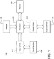
Figure 1 is a block diagram of an example device in which one or more disclosed embodiments may be implemented; -
Figure 2 is an example graphics rendering pipeline in accordance with some embodiments; -
Figure 3 is an example of rendering in a dual graphics processing unit (GPU); -
Figure 4 is an example high level block diagram for frame pacing in accordance with some embodiments; -
Figure 5 is an example flowchart for frame pacing in accordance with some embodiments; -
Figure 6 is another example flowchart for frame pacing in accordance with some embodiments; -
Figure 7 is an example of a sequence diagram for frame pacing in accordance with some embodiments; -
Figure 8 is an example of a sequence diagram for frame pacing in a dual GPU architecture in accordance with some embodiments; -
Figure 9 is an example of a sequence diagram for frame pacing with one timer in accordance with some embodiments; -
Figure 10 is an example of actions in a sequence diagram for frame pacing in accordance with some embodiments; -
Figure 11 is an example diagram of stuttering in a symmetrical architecture; -
Figure 12 is an example diagram of frame pacing or anti-stuttering in a symmetrical architecture in accordance with some embodiments; -
Figure 13 is an example diagram of stuttering in a symmetrical architecture where
-
Figure 14 is an example diagram of stuttering in a symmetrical architecture where TSDMA > TGFX.; -
Figure 15 is an example diagram of stuttering in a slow slave scenario; -
Figure 16 is an example diagram of anti-stuttering in a slow slave scenario in accordance with some embodiments; -
Figure 17 is an example diagram of anti-stuttering in a slow slave scenario where asymmetric crossfire (ACF) is 1:2 and where "1" is the bottleneck, in accordance with some embodiments; and -
Figure 18 is an example diagram of anti-stuttering in a slow slave scenario where ACF is 1:2 and where "2" is the bottleneck, in accordance with some embodiments. - Described herein is a method and system for frame pacing. In general, an estimate is made as to how long it takes to render a frame. This may be done by measuring how long it takes for a graphics processing unit (GPU) to render the frame. An average over several recent frames is used to smooth out differences in workload from frame to frame and render speed of the GPUs. A heartbeat is created that controls the progress of the GPUs and smooths out their presents. The determined appropriate amount of time is waited in the driver, (for example, the kernel mode driver (KMD)), so that the frames are evenly spaced. Frame pacing essentially postpones the flipping of a frame in one GPU that may come too early with respect to another GPU.
-
Figure 1 is a block diagram of anexample device 100 in which one or more disclosed embodiments may be implemented. Thedevice 100 may include, for example, a computer, a gaming device, a handheld device, a set-top box, a television, a mobile phone, or a tablet computer. Thedevice 100 includes aprocessor 102, amemory 104, astorage 106, one ormore input devices 108, and one ormore output devices 110. Thedevice 100 may also optionally include aninput driver 112 and anoutput driver 114. It is understood that thedevice 100 may include additional components not shown inFigure 1 . - The
processor 102 may include a central processing unit (CPU), a graphics processing unit (GPU), a CPU and GPU located on the same die, or one or more processor cores, wherein each processor core may be a CPU or a GPU. Thememory 104 may be located on the same die as theprocessor 102, or may be located separately from theprocessor 102. Thememory 104 may include a volatile or non-volatile memory, for example, random access memory (RAM), dynamic RAM, or a cache. The GPUs may be the same type of GPU (symmetric crossfire) or different types of GPUs (asymmetric crossfire (ACF)). For example, the GPUs in a processor or system may include, but is not limited to, accelerated processing units (APUs), discrete GPUs (dGPUs), and/or combinations thereof. - The
storage 106 may include a fixed or removable storage, for example, a hard disk drive, a solid state drive, an optical disk, or a flash drive. Theinput devices 108 may include a keyboard, a keypad, a touch screen, a touch pad, a detector, a microphone, an accelerometer, a gyroscope, a biometric scanner, or a network connection (e.g., a wireless local area network card for transmission and/or reception of wireless IEEE 802 signals). Theoutput devices 110 may include a display, a speaker, a printer, a haptic feedback device, one or more lights, an antenna, or a network connection (e.g., a wireless local area network card for transmission and/or reception of wireless IEEE 802 signals). - The
input driver 112 communicates with theprocessor 102 and theinput devices 108, and permits theprocessor 102 to receive input from theinput devices 108. Theoutput driver 114 communicates with theprocessor 102 and theoutput devices 110, and permits theprocessor 102 to send output to theoutput devices 110. It is noted that theinput driver 112 and theoutput driver 114 are optional components, and that thedevice 100 will operate in the same manner if theinput driver 112 and theoutput driver 114 are not present. -
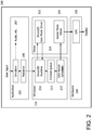
Figure 2 is an examplegraphics rendering pipeline 200. For purposes of illustration and to provide context, the graphics renderingpipeline 200 is shown using a Windows® based operating system (O/S) but any O/S may be used. In general, the graphics renderingpipeline 200 includes an application module/layer/entity 205, a Windows® O/S module/layer/entity 210, a driver module/layer/entity 220 andhardware 230. The term module/layer/entity will be collectively referred to as entity herein. - The
application entity 205 handles, among other functionality, user input. Theapplication entity 205 includes asimulator 207 that updates, for example, object positions, physics and the like with respect to a game world, for example. Thesimulator 207 is coupled or connected, (referred to as connected herein), to arenderer 209 that creates draw calls via, for example, a Direct 3D API, to generate a frame. Therenderer 209 is coupled to a Direct3Druntime entity 211 which parses commands and calls User Mode Driver (UMD) 222 via a DDI interface. TheUMD 222 generates GPU command buffers and submits them to Windows® O/S 210 and in particular, theDirect3D runtime entity 211. The GPU command buffers are then placed in acontext queue 213 until the Windows® O/S 210kernel scheduler 215 is ready to accept them. The GPU command buffers are passed to the Kernel Mode Driver (KMD) 224, which processes them and sends them to theGPU 232. Theapplication entity 205 sends present calls when a frame has finished rendering and can be displayed. The present calls follow the same logical path as the draw calls. -
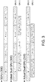
Figure 3 visually illustrates the micro-stuttering issue when using multiple GPU architecture for graphics processing. In general, work assignments or allocations amongst the multiple GPUs use a process called Alternate Frame Rendering (AFR), where each GPU gets its own frame in contrast to each of the multiple GPUs working on a part of the same frame. AFR works well when the output of each GPU is paced such that each GPU is delivering a rendered frame at as even as a rate as possible. For example, as shown inFigure 3 , in a single GPU (SGPU) flow 300, the frames are rendered and presented one after another. In the ideal dual GPU flow 305, the output ofGPU 1 is complete whenGPU 0 is approximately half-way complete with its frame. However, what actually happens is shown in actual dual GPU flow 310. If the frame forGPU 1 is completed near whenGPU 0 completes rendering, then the first frame rendered will be displayed on the screen for less time than the second or subsequent frame. If the amount of time that frames are displayed is not evenly spaced, the user may visually see and perceive lower frame rates, i.e., micro-stuttering. - Described herein is a method and system for frame pacing.
-
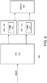
Figure 4 shows an example of a twoGPU architecture 400;Figure 5 shows ahigh level flowchart 500;Figure 6 shows an example flowchart for the twoGPU architecture 400; andFigure 7 shows a high level example of frame pacing flow or sequence 600 from an UMD perspective for the twoGPU architecture 400. These figures collectively illustrate frame pacing as described herein. The system architecture may include any number of CPUs, GPUs, processors and the like without deviating from the scope of the invention described herein. In particular, the twoGPU architecture 400 include aCPU 405 coupled toGPU 410 andGPU 415, which in turn are coupled to adisplay 420. EachGPU timer 412 and 417 to signal starting and completion of the delay as described herein below. - Referring now to
Figures 4 and5 , an estimate is made as to how long it takes to render a frame (505). This may be done by measuring how long it takes for theGPUs - Referring now to
Figures 6 and7 , for the twoGPU architecture 400, a render command is sent to GPU 0 (605). The UMD, (a UMD is shown inFigure 2 ), submits a delay request to a dummy engine in the KMD, (a KMD is shown inFigure 2 ), (610). This is shown as a "Delay" in the dummy engine flow inFigure 7 . As described and shown herein below, the Delay effectively provides a minimum amount of time after which a GPU can present. That is, if the rendering process is complete prior to the running of the Delay, then the GPU presents after the running of the Delay. A signal is sent by the dummy engine to GPU 0 (615). This is shown as "S" inFigure 7 .GPU 0 waits the requisite delay time (620). This is shown as "W" inFigure 7 .GPU 0 presents after the requisite delay time (625). This is shown by the "P" inFigure 7 . The sequence is then repeated forGPU 1. In particular, a render command is sent to GPU 1 (630). The UMD submits a delay request to a dummy engine in the KMD (635). A signal is sent by the dummy engine to GPU 1 (640).GPU 1 waits the requisite delay time (645).GPU 1 presents after the requisite delay time (650) is over and the rendering process is complete. That is, the present can be no earlier than the delay period and only if the rendering process is also complete. The sequence is then repeated forGPU 0 andGPU 1. -
Figure 8 shows another high level example of frame pacing flow orsequence 800. A rendercommand 805 is sent toGPU 0 and a render command 810 is sent toGPU 1. TheGPU 0 presents (P) 815 and also signals (S) 820 a timer on GPU 0 (via a UMD as shown inFigure 2 ) to wait (W) 825 a certain amount of time (Delay) 830 beforeGPU 1 presents. After waiting the Delay 830 (as shown by the "bubble"), the timer onGPU 0 sends a signal (S) 835 toGPU 1 that the wait (W) 840 is over and thatGPU 1 can present (P) 845. TheGPU 1 then signals (S) 850 a timer on GPU 1 (via a UMD as shown inFigure 2 ) to wait (W) 855 a certain amount of time (Delay) 860 beforeGPU 0 presents. In this instance, theDelay 860 coincides with the time needed byGPU 0 to complete the rendering process. This is illustrated by the fact that no "bubble" is shown in the later sequences. Effectively, once the Delay is introduced to offset the rendering processing betweenGPU 0 andGPU 1 and align the processing betweenGPU 0 andGPU 1, then the offset will always be present and the delay will have nearly no effect on throughput or frame rate. If for some reason, one of the GPUs does get out of alignment, the offset will correct the alignment. - In an embodiment, frame pacing may affect present device driver interfaces (DDIs) and not non-present DDIs.
- In the embodiments described herein, the calculations for frame time and managing are done in the UMD. In other embodiments, the calculations for frame time and managing are done in the KMD.
- In an embodiment, the amount of delay may be tuned.
- In an embodiment, one timer may be used to implement frame pacing in a multiple GPU architecture. This is illustrated in
Figure 9 and works similarly toFigure 8 except that one timer is used. - In an embodiment, the frame pacing described herein may be utilized in hardware compositing architecture, hardware flipping architecture and/or a software compositing architecture.
- Referring to
Figure 10 , there is an example illustration of timestamp queries as described herein above. In particular,Figure 10 shows the actions on dual-GPUs. Two query objects are used in every frame - one at the beginning of a frame, denoted as (Q), and one at the end of a frame, denoted as (Q'). A GetData, (G for Q and G' for Q'), on a query object retrieves the time when the query object is processed by the GPU. The interval between Q and Q' is the frame time. BeginFrame() is called at the beginning of a frame, and inserts Q to a GPU. EndFrame() is called at the end of a frame, and inserts Q' to a GPU, (the number inFigure 10 shows when this call happens in an example driver). - On a multi-GPU system, it is possible only the Master GPU (GPU 0) is driving screen outputs while other GPU(s) are not. Software compositing is used in this scenario which copies every Slave frame to the Master GPU for display. Software compositing suffers micro-stuttering as well as hardware compositing.
Figure 11 shows an example of symmetrical crossfire (1:1) stuttering, where symmetrical crossfire means the same type of GPUs are being used in the processor or system. An extra surface (0) is created onGPU 0 to eliminate tearing. A thick weighted vertical line is a flip on the master's 3D engine while a dashed line is on the master's SDMA engine. A thin weighted shadow box stands for a software compositing SDMA transfer and its target. Other boxes are 3D cmdbufs - the number in a box is the frame number, the letter is the render target. For each Slave frame, three operations need to be serialized:GPU 1 finishes rendering the frame on its 3D engine;GPU 1 transfers the frame toGPU 0 via its SDMA engine, andGPU 0 presents the frame to on-screen via its SDMA engine. It isclear frames frames - In a dual GPU architecture example, a timer on
GPU 0 with a delay is used to implement frame pacing as shown inFigure 12 , where all presents are of equal length. The delay may be computed as shown in Equation 1:
time GPU 0 takes to render a frame, GfxTime Gpu1 is thetime GPU 1 takes to render a frame and SdmaTime is the time the SDMA engine takes to transfer a frame fromGPU 1 toGPU 0. - In an example of slow transfer, assume
GPU 0 andGPU 1 takes the same time to render a frame, TGFX = GfxTime Gpu0 = GfxTime Gpu1 . If
GPU 1 completes earlier than frame N onGPU 0. As shown inFigure 13 ,frame 5 is done beforeframe 4,frame 7 is done beforeframe 6, and so on. This layout is vulnerable to cross-GPU resource transfers.Figure 14 show an example of where transfer is the bottleneck and TSDMA > TGFX. Although the above slow transfer issue is theoretically possible, the slow transfer example has no practical effect in real world applications. -
Figures 15-18 are similar toFigures 11-14 , but for the asymmetric crossfire (ACF) architecture where the GPUs don't render at the same rate.Figures 17 and18 show ACF when the AFR ratio is unbalanced at 1:2, that is one GPU renders 2 out of 3 frames. -
Figure 15 shows an example of a slow slave issue with ACF 1:1 andFigure 16 shows a frame pacing implementation to address slow slave issues. - In ACF 1:2 architecture, whether to flip the master's frames on 3D or SDMA does not matter. The reason is that
frame 5 has to wait for B to be off screen. -
Figure 17 shows how a solution for ACF 1:2, where "1" is the bottleneck and GfxTime Gpu1 is the sum of two successive frames onGPU 1. -
Figure 18 shows how a solution for ACF 1:2, where "2" is the bottleneck. - In general, a method for frame pacing in a rendering process includes estimating a frame rendering time for each of a plurality of graphics processing units (GPUs), determining a delay based on at least an estimated frame rendering time and inserting the delay into the rendering process to render frames in an evenly spaced manner. In an embodiment, the delay may be dynamically adjusted based on application workload on the GPUs. In an example, the estimated frame rendering time is an average taken over a predetermined amount of frames. In an example, a heartbeat is established based on at least the delay to control the rendering process and frame presents. In an example, at least one timer is used to enable the delay. In an example, timestamp queries are used for determining the estimated frame rendering time. In an example, the delay is implemented in a kernel mode driver (KMD). A dummy schedulable engine is created in the KMD to implement the delay. A present occurs at the latter of expiration of the delay or completion of the rendering process.
- A system for frame pacing in a rendering process includes a first processing module configured to estimate a frame rendering time for each of a plurality of graphics processing units (GPUs). The first processing module is configured to determine a delay based on at least an estimated frame rendering time. A second processing module is configured to insert the delay into the rendering process to render frames in an evenly spaced manner. In an embodiment, the delay may be dynamically adjusted based on application workload on the GPUs. In an example, the estimated frame rendering time is an average taken over a predetermined amount of frames. In an example, a heartbeat is established based on at least the delay to control the rendering process and frame presents. In an example, at least one timer is used to enable the delay. In an example, timestamp queries are used for determining the estimated frame rendering time. In an example, the second processing module is a kernel mode driver (KMD). A dummy schedulable engine is created in the KMD to implement the delay. A present occurs at the latter of expiration of the delay or completion of the rendering process. In an example, the first processing module may be a UMD and the second processing unit may be a KMD.
- It should be understood that many variations are possible based on the disclosure herein. Although features and elements are described above in particular combinations, each feature or element may be used alone without the other features and elements or in various combinations with or without other features and elements.
- The methods provided may be implemented in a general purpose computer, a processor, or a processor core. Suitable processors include, by way of example, a general purpose processor, a special purpose processor, a conventional processor, a digital signal processor (DSP), a plurality of microprocessors, one or more microprocessors in association with a DSP core, a controller, a microcontroller, Application Specific Integrated Circuits (ASICs), Field Programmable Gate Arrays (FPGAs) circuits, any other type of integrated circuit (IC), and/or a state machine. Such processors may be manufactured by configuring a manufacturing process using the results of processed hardware description language (HDL) instructions and other intermediary data including netlists (such instructions capable of being stored on a computer readable media). The results of such processing may be maskworks that are then used in a semiconductor manufacturing process to manufacture a processor which implements aspects of the present invention.
- The methods or flow charts provided herein may be implemented in a computer program, software, or firmware incorporated in a computer-readable storage medium for execution by a general purpose computer or a processor. Examples of computer-readable storage mediums include a read only memory (ROM), a random access memory (RAM), a register, cache memory, semiconductor memory devices, magnetic media such as internal hard disks and removable disks, magneto-optical media, and optical media such as CD-ROM disks, and digital versatile disks (DVDs).
Claims (14)
- A computer implemented method for frame pacing in a rendering process, the method comprising:estimating, for each graphics processing unit "GPU" (410) of a plurality of GPUs, a frame rendering time, wherein the frame rendering time is an estimate of how long each GPU takes to render a frame;determining a delay based on the estimated frame rendering time for each of the plurality of GPUs; andinserting the delay into the rendering process to render frames in an evenly spaced temporal manner, characterized in that the delay is implemented in a kernel mode driver, and wherein the delay is signalled by a dummy schedulable engine in the kernel mode driver to each GPU to cause a wait time in the rendering process.
- The method of claim 1, wherein the delay is dynamically adjusted based on application workload for each GPU in the plurality of GPUs.
- The method of claim 1, wherein the estimated frame rendering time for each GPU is an average taken over a predetermined amount of frames.
- The method of claim 1, wherein a heartbeat is established based on at least the delay to control the rendering process and frame presents, wherein the heartbeat is a steady ticking of when frames should be presented.
- The method of claim 1, wherein at least one timer is used to enable the delay.
- The method of claim 1, wherein timestamp queries are used for determining the estimated frame rendering time for each GPU.
- The method of claim 1, wherein a dummy schedulable engine is created in the kernel mode driver to implement the delay, the dummy schedulable engine scheduling configured to signal the delay to cause a wait time in the rendering process in response to a request.
- The method of claim 1, wherein a present occurs at the latter of expiration of the delay or completion of the rendering process, wherein the present means a frame can be displayed.
- 10. A system for frame pacing in a rendering process, comprising:a first processing module configured to estimate a frame rendering time for each of a plurality of graphics processing units "GPUs" (410,415), wherein the frame rendering time is an estimate of how long each GPU takes to render a frame;the first processing module configured to determine a delay based on the estimated frame rendering time for each of the plurality of GPUs; anda second processing module configured to insert the delay into the rendering process to render frames in an evenly spaced temporal manner, wherein the delay is implemented in a kernel mode driver, and characterized in that the delay is signalled by the a dummy schedulable engine in the kernel mode driver to each GPU to cause a wait time in the rendering process.
- The system of claim 9, wherein the delay is dynamically adjusted based on application workload for each GPU in the plurality of GPUs.
- The system of claim 9, wherein the estimated frame rendering time for each GPU is an average taken over a predetermined amount of frames.
- The system of claim 9, wherein a heartbeat is established based on at least the delay to control the rendering process and frame presents, wherein the heartbeat is a steady ticking of when frames should be presented and the present means a frame can be displayed.
- The system of claim 9, wherein timestamp queries are used for determining the estimated frame rendering time for each GPU.
- The system of claim 9, wherein the second processing module is a kernel mode driver "KMD" and a dummy schedulable engine is created in the KMD to implement the delay, wherein the dummy schedulable engine scheduling configured to signal the delay to cause a wait time in the rendering process in response to a request.
Applications Claiming Priority (2)
| Application Number | Priority Date | Filing Date | Title |
|---|---|---|---|
| US201462035124P | 2014-08-08 | 2014-08-08 | |
| PCT/US2015/044128 WO2016022874A1 (en) | 2014-08-08 | 2015-08-07 | Method and system for frame pacing |
Publications (3)
| Publication Number | Publication Date |
|---|---|
| EP3178065A1 EP3178065A1 (en) | 2017-06-14 |
| EP3178065A4 EP3178065A4 (en) | 2018-01-24 |
| EP3178065B1 true EP3178065B1 (en) | 2020-04-08 |
Family
ID=55264602
Family Applications (1)
| Application Number | Title | Priority Date | Filing Date |
|---|---|---|---|
| EP15829257.3A Active EP3178065B1 (en) | 2014-08-08 | 2015-08-07 | Method and system for frame pacing |
Country Status (6)
| Country | Link |
|---|---|
| US (1) | US9679345B2 (en) |
| EP (1) | EP3178065B1 (en) |
| JP (1) | JP6633614B2 (en) |
| KR (1) | KR102476197B1 (en) |
| CN (1) | CN106575302B (en) |
| WO (1) | WO2016022874A1 (en) |
Families Citing this family (9)
| Publication number | Priority date | Publication date | Assignee | Title |
|---|---|---|---|---|
| KR102606693B1 (en) * | 2016-08-23 | 2023-11-28 | 삼성전자 주식회사 | Electronic device and method for controlling operation thereof |
| US20180329742A1 (en) * | 2017-05-10 | 2018-11-15 | Mediatek Inc. | Timer-assisted frame running time estimation |
| CN109474768A (en) * | 2017-09-08 | 2019-03-15 | 中兴通讯股份有限公司 | A kind of method and device improving image fluency |
| CN108769785B (en) * | 2018-06-29 | 2020-11-03 | 京东方科技集团股份有限公司 | Video playing method, device and storage medium |
| GB202012559D0 (en) * | 2020-08-12 | 2020-09-23 | Samsung Electronics Co Ltd | Reducing latency between receiving user input and displaying resulting frame |
| US20220122566A1 (en) * | 2020-10-16 | 2022-04-21 | Intel Corporation | Frame pacing for improved experiences in 3d applications |
| US11935149B2 (en) | 2020-11-13 | 2024-03-19 | Samsung Electronics Co., Ltd | Electronic device and image rendering method thereof for adjusting frame rate |
| CN112954402B (en) * | 2021-03-11 | 2023-04-28 | 北京字节跳动网络技术有限公司 | Video display method, apparatus and storage medium |
| CN115375530A (en) * | 2022-07-13 | 2022-11-22 | 北京松应科技有限公司 | Multi-GPU collaborative rendering method, system, device and storage medium |
Family Cites Families (14)
| Publication number | Priority date | Publication date | Assignee | Title |
|---|---|---|---|---|
| JP2002328818A (en) * | 2001-02-27 | 2002-11-15 | Sony Computer Entertainment Inc | Information processor, integrated information processor, method for calculating execution load and computer program |
| US6919900B2 (en) * | 2001-03-23 | 2005-07-19 | Microsoft Corporation | Methods and systems for preparing graphics for display on a computing device |
| GB2406184B (en) * | 2003-09-17 | 2006-03-15 | Advanced Risc Mach Ltd | Data processing system |
| US7545380B1 (en) | 2004-12-16 | 2009-06-09 | Nvidia Corporation | Sequencing of displayed images for alternate frame rendering in a multi-processor graphics system |
| US7525549B1 (en) * | 2004-12-16 | 2009-04-28 | Nvidia Corporation | Display balance/metering |
| US7364306B2 (en) * | 2005-06-20 | 2008-04-29 | Digital Display Innovations, Llc | Field sequential light source modulation for a digital display system |
| JP4185086B2 (en) * | 2005-09-28 | 2008-11-19 | 株式会社日立国際電気 | Image processing device |
| JP5231886B2 (en) | 2008-07-11 | 2013-07-10 | キヤノン株式会社 | Image processing apparatus and control method thereof |
| US8484647B2 (en) * | 2009-07-24 | 2013-07-09 | Apple Inc. | Selectively adjusting CPU wait mode based on estimation of remaining work before task completion on GPU |
| US9524138B2 (en) * | 2009-12-29 | 2016-12-20 | Nvidia Corporation | Load balancing in a system with multi-graphics processors and multi-display systems |
| JP5662418B2 (en) * | 2010-03-24 | 2015-01-28 | パナソニック インテレクチュアル プロパティ コーポレーション オブアメリカPanasonic Intellectual Property Corporation of America | Display processing apparatus, display processing method, and integrated circuit |
| WO2012154155A1 (en) | 2011-05-06 | 2012-11-15 | Google Inc. | Apparatus and method for determining a video frame's estimated arrival time |
| WO2012154152A1 (en) | 2011-05-06 | 2012-11-15 | Google Inc. | Apparatus and method for rendering video with retransmission delay |
| US9940904B2 (en) * | 2013-10-23 | 2018-04-10 | Intel Corporation | Techniques for determining an adjustment for a visual output |
-
2015
- 2015-08-06 US US14/820,221 patent/US9679345B2/en active Active
- 2015-08-07 EP EP15829257.3A patent/EP3178065B1/en active Active
- 2015-08-07 CN CN201580042084.8A patent/CN106575302B/en active Active
- 2015-08-07 KR KR1020177004860A patent/KR102476197B1/en active IP Right Grant
- 2015-08-07 JP JP2017506881A patent/JP6633614B2/en active Active
- 2015-08-07 WO PCT/US2015/044128 patent/WO2016022874A1/en active Application Filing
Non-Patent Citations (1)
| Title |
|---|
| None * |
Also Published As
| Publication number | Publication date |
|---|---|
| CN106575302B (en) | 2019-08-30 |
| JP2017531232A (en) | 2017-10-19 |
| KR102476197B1 (en) | 2022-12-09 |
| US20160042488A1 (en) | 2016-02-11 |
| EP3178065A4 (en) | 2018-01-24 |
| EP3178065A1 (en) | 2017-06-14 |
| CN106575302A (en) | 2017-04-19 |
| US9679345B2 (en) | 2017-06-13 |
| WO2016022874A1 (en) | 2016-02-11 |
| KR20170041760A (en) | 2017-04-17 |
| JP6633614B2 (en) | 2020-01-22 |
Similar Documents
| Publication | Publication Date | Title |
|---|---|---|
| EP3178065B1 (en) | Method and system for frame pacing | |
| JP6467062B2 (en) | Backward compatibility using spoof clock and fine grain frequency control | |
| US10078882B2 (en) | Priority-based command execution | |
| US8300056B2 (en) | Seamless display migration | |
| CN103176689B (en) | interface switching method and system | |
| WO2010053956A3 (en) | Command buffers for web-based graphics rendering | |
| US20160260246A1 (en) | Providing asynchronous display shader functionality on a shared shader core | |
| CN110494837B (en) | Ink rendering using high priority queues | |
| KR20220143667A (en) | Reduced display processing unit delivery time to compensate for delayed graphics processing unit render times | |
| TWI352935B (en) | Work based clock management for display sub-system | |
| US20210327020A1 (en) | Method and apparatus for directing application requests for rendering | |
| US10733687B2 (en) | Method and apparatus for data communication in virtualized environment, and processor | |
| US20140204005A1 (en) | System, method, and computer program product for distributed processing of overlapping portions of pixels | |
| US10528685B2 (en) | Efficient mechanism in hardware and software co-simulation system | |
| US20190197663A1 (en) | Graphics processor that performs warping, rendering system having the graphics processor, and method of operating the graphics processor | |
| US9632848B1 (en) | Asynchronous submission of commands | |
| EP3522530A1 (en) | System performance improvement method, system performance improvement device and display device | |
| US20220013087A1 (en) | Methods and apparatus for display processor enhancement | |
| CN114661260A (en) | Balancing alternate frame times on a variable refresh rate display | |
| JP2017127679A5 (en) | ||
| JP2017127676A5 (en) | ||
| US11922533B2 (en) | Dynamically reducing latency in processing pipelines | |
| KR20130105088A (en) | Apparatus and method for rendering based on tile for controlling multiple pixel core | |
| EP3218869A1 (en) | Sort-free threading model for a multi-threaded graphics pipeline | |
| CN115964160A (en) | Kernel optimization and deferred execution |
Legal Events
| Date | Code | Title | Description |
|---|---|---|---|
| STAA | Information on the status of an ep patent application or granted ep patent |
Free format text: STATUS: THE INTERNATIONAL PUBLICATION HAS BEEN MADE |
|
| PUAI | Public reference made under article 153(3) epc to a published international application that has entered the european phase |
Free format text: ORIGINAL CODE: 0009012 |
|
| STAA | Information on the status of an ep patent application or granted ep patent |
Free format text: STATUS: REQUEST FOR EXAMINATION WAS MADE |
|
| 17P | Request for examination filed |
Effective date: 20170130 |
|
| AK | Designated contracting states |
Kind code of ref document: A1 Designated state(s): AL AT BE BG CH CY CZ DE DK EE ES FI FR GB GR HR HU IE IS IT LI LT LU LV MC MK MT NL NO PL PT RO RS SE SI SK SM TR |
|
| AX | Request for extension of the european patent |
Extension state: BA ME |
|
| DAV | Request for validation of the european patent (deleted) | ||
| DAX | Request for extension of the european patent (deleted) | ||
| A4 | Supplementary search report drawn up and despatched |
Effective date: 20171222 |
|
| RIC1 | Information provided on ipc code assigned before grant |
Ipc: G06T 1/20 20060101ALI20171218BHEP Ipc: G06T 15/00 20110101AFI20171218BHEP |
|
| RAP1 | Party data changed (applicant data changed or rights of an application transferred) |
Owner name: ADVANCED MICRO DEVICES, INC. |
|
| RAP1 | Party data changed (applicant data changed or rights of an application transferred) |
Owner name: ADVANCED MICRO DEVICES, INC. |
|
| STAA | Information on the status of an ep patent application or granted ep patent |
Free format text: STATUS: EXAMINATION IS IN PROGRESS |
|
| 17Q | First examination report despatched |
Effective date: 20181001 |
|
| GRAP | Despatch of communication of intention to grant a patent |
Free format text: ORIGINAL CODE: EPIDOSNIGR1 |
|
| STAA | Information on the status of an ep patent application or granted ep patent |
Free format text: STATUS: GRANT OF PATENT IS INTENDED |
|
| INTG | Intention to grant announced |
Effective date: 20191111 |
|
| GRAS | Grant fee paid |
Free format text: ORIGINAL CODE: EPIDOSNIGR3 |
|
| GRAA | (expected) grant |
Free format text: ORIGINAL CODE: 0009210 |
|
| STAA | Information on the status of an ep patent application or granted ep patent |
Free format text: STATUS: THE PATENT HAS BEEN GRANTED |
|
| AK | Designated contracting states |
Kind code of ref document: B1 Designated state(s): AL AT BE BG CH CY CZ DE DK EE ES FI FR GB GR HR HU IE IS IT LI LT LU LV MC MK MT NL NO PL PT RO RS SE SI SK SM TR |
|
| REG | Reference to a national code |
Ref country code: CH Ref legal event code: EP Ref country code: AT Ref legal event code: REF Ref document number: 1255399 Country of ref document: AT Kind code of ref document: T Effective date: 20200415 |
|
| REG | Reference to a national code |
Ref country code: DE Ref legal event code: R096 Ref document number: 602015050451 Country of ref document: DE |
|
| REG | Reference to a national code |
Ref country code: IE Ref legal event code: FG4D |
|
| REG | Reference to a national code |
Ref country code: NL Ref legal event code: MP Effective date: 20200408 |
|
| REG | Reference to a national code |
Ref country code: LT Ref legal event code: MG4D |
|
| PG25 | Lapsed in a contracting state [announced via postgrant information from national office to epo] |
Ref country code: NL Free format text: LAPSE BECAUSE OF FAILURE TO SUBMIT A TRANSLATION OF THE DESCRIPTION OR TO PAY THE FEE WITHIN THE PRESCRIBED TIME-LIMIT Effective date: 20200408 Ref country code: LT Free format text: LAPSE BECAUSE OF FAILURE TO SUBMIT A TRANSLATION OF THE DESCRIPTION OR TO PAY THE FEE WITHIN THE PRESCRIBED TIME-LIMIT Effective date: 20200408 Ref country code: FI Free format text: LAPSE BECAUSE OF FAILURE TO SUBMIT A TRANSLATION OF THE DESCRIPTION OR TO PAY THE FEE WITHIN THE PRESCRIBED TIME-LIMIT Effective date: 20200408 Ref country code: PT Free format text: LAPSE BECAUSE OF FAILURE TO SUBMIT A TRANSLATION OF THE DESCRIPTION OR TO PAY THE FEE WITHIN THE PRESCRIBED TIME-LIMIT Effective date: 20200817 Ref country code: IS Free format text: LAPSE BECAUSE OF FAILURE TO SUBMIT A TRANSLATION OF THE DESCRIPTION OR TO PAY THE FEE WITHIN THE PRESCRIBED TIME-LIMIT Effective date: 20200808 Ref country code: SE Free format text: LAPSE BECAUSE OF FAILURE TO SUBMIT A TRANSLATION OF THE DESCRIPTION OR TO PAY THE FEE WITHIN THE PRESCRIBED TIME-LIMIT Effective date: 20200408 Ref country code: GR Free format text: LAPSE BECAUSE OF FAILURE TO SUBMIT A TRANSLATION OF THE DESCRIPTION OR TO PAY THE FEE WITHIN THE PRESCRIBED TIME-LIMIT Effective date: 20200709 Ref country code: NO Free format text: LAPSE BECAUSE OF FAILURE TO SUBMIT A TRANSLATION OF THE DESCRIPTION OR TO PAY THE FEE WITHIN THE PRESCRIBED TIME-LIMIT Effective date: 20200708 |
|
| REG | Reference to a national code |
Ref country code: AT Ref legal event code: MK05 Ref document number: 1255399 Country of ref document: AT Kind code of ref document: T Effective date: 20200408 |
|
| PG25 | Lapsed in a contracting state [announced via postgrant information from national office to epo] |
Ref country code: HR Free format text: LAPSE BECAUSE OF FAILURE TO SUBMIT A TRANSLATION OF THE DESCRIPTION OR TO PAY THE FEE WITHIN THE PRESCRIBED TIME-LIMIT Effective date: 20200408 Ref country code: RS Free format text: LAPSE BECAUSE OF FAILURE TO SUBMIT A TRANSLATION OF THE DESCRIPTION OR TO PAY THE FEE WITHIN THE PRESCRIBED TIME-LIMIT Effective date: 20200408 Ref country code: LV Free format text: LAPSE BECAUSE OF FAILURE TO SUBMIT A TRANSLATION OF THE DESCRIPTION OR TO PAY THE FEE WITHIN THE PRESCRIBED TIME-LIMIT Effective date: 20200408 Ref country code: BG Free format text: LAPSE BECAUSE OF FAILURE TO SUBMIT A TRANSLATION OF THE DESCRIPTION OR TO PAY THE FEE WITHIN THE PRESCRIBED TIME-LIMIT Effective date: 20200708 |
|
| PG25 | Lapsed in a contracting state [announced via postgrant information from national office to epo] |
Ref country code: AL Free format text: LAPSE BECAUSE OF FAILURE TO SUBMIT A TRANSLATION OF THE DESCRIPTION OR TO PAY THE FEE WITHIN THE PRESCRIBED TIME-LIMIT Effective date: 20200408 |
|
| REG | Reference to a national code |
Ref country code: DE Ref legal event code: R097 Ref document number: 602015050451 Country of ref document: DE |
|
| PG25 | Lapsed in a contracting state [announced via postgrant information from national office to epo] |
Ref country code: CZ Free format text: LAPSE BECAUSE OF FAILURE TO SUBMIT A TRANSLATION OF THE DESCRIPTION OR TO PAY THE FEE WITHIN THE PRESCRIBED TIME-LIMIT Effective date: 20200408 Ref country code: ES Free format text: LAPSE BECAUSE OF FAILURE TO SUBMIT A TRANSLATION OF THE DESCRIPTION OR TO PAY THE FEE WITHIN THE PRESCRIBED TIME-LIMIT Effective date: 20200408 Ref country code: EE Free format text: LAPSE BECAUSE OF FAILURE TO SUBMIT A TRANSLATION OF THE DESCRIPTION OR TO PAY THE FEE WITHIN THE PRESCRIBED TIME-LIMIT Effective date: 20200408 Ref country code: SM Free format text: LAPSE BECAUSE OF FAILURE TO SUBMIT A TRANSLATION OF THE DESCRIPTION OR TO PAY THE FEE WITHIN THE PRESCRIBED TIME-LIMIT Effective date: 20200408 Ref country code: DK Free format text: LAPSE BECAUSE OF FAILURE TO SUBMIT A TRANSLATION OF THE DESCRIPTION OR TO PAY THE FEE WITHIN THE PRESCRIBED TIME-LIMIT Effective date: 20200408 Ref country code: RO Free format text: LAPSE BECAUSE OF FAILURE TO SUBMIT A TRANSLATION OF THE DESCRIPTION OR TO PAY THE FEE WITHIN THE PRESCRIBED TIME-LIMIT Effective date: 20200408 Ref country code: AT Free format text: LAPSE BECAUSE OF FAILURE TO SUBMIT A TRANSLATION OF THE DESCRIPTION OR TO PAY THE FEE WITHIN THE PRESCRIBED TIME-LIMIT Effective date: 20200408 Ref country code: IT Free format text: LAPSE BECAUSE OF FAILURE TO SUBMIT A TRANSLATION OF THE DESCRIPTION OR TO PAY THE FEE WITHIN THE PRESCRIBED TIME-LIMIT Effective date: 20200408 |
|
| PLBE | No opposition filed within time limit |
Free format text: ORIGINAL CODE: 0009261 |
|
| STAA | Information on the status of an ep patent application or granted ep patent |
Free format text: STATUS: NO OPPOSITION FILED WITHIN TIME LIMIT |
|
| PG25 | Lapsed in a contracting state [announced via postgrant information from national office to epo] |
Ref country code: PL Free format text: LAPSE BECAUSE OF FAILURE TO SUBMIT A TRANSLATION OF THE DESCRIPTION OR TO PAY THE FEE WITHIN THE PRESCRIBED TIME-LIMIT Effective date: 20200408 Ref country code: SK Free format text: LAPSE BECAUSE OF FAILURE TO SUBMIT A TRANSLATION OF THE DESCRIPTION OR TO PAY THE FEE WITHIN THE PRESCRIBED TIME-LIMIT Effective date: 20200408 |
|
| 26N | No opposition filed |
Effective date: 20210112 |
|
| PG25 | Lapsed in a contracting state [announced via postgrant information from national office to epo] |
Ref country code: MC Free format text: LAPSE BECAUSE OF FAILURE TO SUBMIT A TRANSLATION OF THE DESCRIPTION OR TO PAY THE FEE WITHIN THE PRESCRIBED TIME-LIMIT Effective date: 20200408 |
|
| REG | Reference to a national code |
Ref country code: CH Ref legal event code: PL |
|
| PG25 | Lapsed in a contracting state [announced via postgrant information from national office to epo] |
Ref country code: LU Free format text: LAPSE BECAUSE OF NON-PAYMENT OF DUE FEES Effective date: 20200807 Ref country code: LI Free format text: LAPSE BECAUSE OF NON-PAYMENT OF DUE FEES Effective date: 20200831 Ref country code: CH Free format text: LAPSE BECAUSE OF NON-PAYMENT OF DUE FEES Effective date: 20200831 |
|
| REG | Reference to a national code |
Ref country code: BE Ref legal event code: MM Effective date: 20200831 |
|
| PG25 | Lapsed in a contracting state [announced via postgrant information from national office to epo] |
Ref country code: SI Free format text: LAPSE BECAUSE OF FAILURE TO SUBMIT A TRANSLATION OF THE DESCRIPTION OR TO PAY THE FEE WITHIN THE PRESCRIBED TIME-LIMIT Effective date: 20200408 |
|
| PG25 | Lapsed in a contracting state [announced via postgrant information from national office to epo] |
Ref country code: FR Free format text: LAPSE BECAUSE OF NON-PAYMENT OF DUE FEES Effective date: 20200831 |
|
| PG25 | Lapsed in a contracting state [announced via postgrant information from national office to epo] |
Ref country code: BE Free format text: LAPSE BECAUSE OF NON-PAYMENT OF DUE FEES Effective date: 20200831 Ref country code: IE Free format text: LAPSE BECAUSE OF NON-PAYMENT OF DUE FEES Effective date: 20200807 |
|
| PG25 | Lapsed in a contracting state [announced via postgrant information from national office to epo] |
Ref country code: TR Free format text: LAPSE BECAUSE OF FAILURE TO SUBMIT A TRANSLATION OF THE DESCRIPTION OR TO PAY THE FEE WITHIN THE PRESCRIBED TIME-LIMIT Effective date: 20200408 Ref country code: MT Free format text: LAPSE BECAUSE OF FAILURE TO SUBMIT A TRANSLATION OF THE DESCRIPTION OR TO PAY THE FEE WITHIN THE PRESCRIBED TIME-LIMIT Effective date: 20200408 Ref country code: CY Free format text: LAPSE BECAUSE OF FAILURE TO SUBMIT A TRANSLATION OF THE DESCRIPTION OR TO PAY THE FEE WITHIN THE PRESCRIBED TIME-LIMIT Effective date: 20200408 |
|
| PG25 | Lapsed in a contracting state [announced via postgrant information from national office to epo] |
Ref country code: MK Free format text: LAPSE BECAUSE OF FAILURE TO SUBMIT A TRANSLATION OF THE DESCRIPTION OR TO PAY THE FEE WITHIN THE PRESCRIBED TIME-LIMIT Effective date: 20200408 |
|
| P01 | Opt-out of the competence of the unified patent court (upc) registered |
Effective date: 20230530 |
|
| PGFP | Annual fee paid to national office [announced via postgrant information from national office to epo] |
Ref country code: GB Payment date: 20230823 Year of fee payment: 9 |
|
| PGFP | Annual fee paid to national office [announced via postgrant information from national office to epo] |
Ref country code: DE Payment date: 20230818 Year of fee payment: 9 |