EP3177121A1 - Electric device and method for assembling such an electric device - Google Patents
Electric device and method for assembling such an electric device Download PDFInfo
- Publication number
- EP3177121A1 EP3177121A1 EP16201059.9A EP16201059A EP3177121A1 EP 3177121 A1 EP3177121 A1 EP 3177121A1 EP 16201059 A EP16201059 A EP 16201059A EP 3177121 A1 EP3177121 A1 EP 3177121A1
- Authority
- EP
- European Patent Office
- Prior art keywords
- electronic unit
- insulating material
- zone
- electrical
- electrical device
- Prior art date
- Legal status (The legal status is an assumption and is not a legal conclusion. Google has not performed a legal analysis and makes no representation as to the accuracy of the status listed.)
- Granted
Links
- 238000000034 method Methods 0.000 title claims description 23
- 239000011810 insulating material Substances 0.000 claims abstract description 88
- 238000011049 filling Methods 0.000 claims description 13
- 238000000151 deposition Methods 0.000 claims description 6
- 238000002955 isolation Methods 0.000 description 7
- 239000000463 material Substances 0.000 description 7
- 238000009413 insulation Methods 0.000 description 6
- 238000001816 cooling Methods 0.000 description 5
- 230000000295 complement effect Effects 0.000 description 4
- 239000000499 gel Substances 0.000 description 4
- 238000004519 manufacturing process Methods 0.000 description 4
- 230000004087 circulation Effects 0.000 description 3
- 239000000428 dust Substances 0.000 description 3
- 239000007788 liquid Substances 0.000 description 3
- 239000007789 gas Substances 0.000 description 2
- 239000012212 insulator Substances 0.000 description 2
- 230000008569 process Effects 0.000 description 2
- 230000001603 reducing effect Effects 0.000 description 2
- 239000007858 starting material Substances 0.000 description 2
- 206010013647 Drowning Diseases 0.000 description 1
- 230000008021 deposition Effects 0.000 description 1
- 238000009792 diffusion process Methods 0.000 description 1
- 230000000694 effects Effects 0.000 description 1
- 239000003822 epoxy resin Substances 0.000 description 1
- 238000003780 insertion Methods 0.000 description 1
- 230000037431 insertion Effects 0.000 description 1
- 230000000670 limiting effect Effects 0.000 description 1
- 239000002991 molded plastic Substances 0.000 description 1
- 229920000647 polyepoxide Polymers 0.000 description 1
- 229920001296 polysiloxane Polymers 0.000 description 1
- 238000011084 recovery Methods 0.000 description 1
- 230000009467 reduction Effects 0.000 description 1
- 229920005989 resin Polymers 0.000 description 1
- 239000011347 resin Substances 0.000 description 1
- 238000012546 transfer Methods 0.000 description 1
Images


Classifications
-
- H—ELECTRICITY
- H02—GENERATION; CONVERSION OR DISTRIBUTION OF ELECTRIC POWER
- H02K—DYNAMO-ELECTRIC MACHINES
- H02K11/00—Structural association of dynamo-electric machines with electric components or with devices for shielding, monitoring or protection
- H02K11/30—Structural association with control circuits or drive circuits
- H02K11/33—Drive circuits, e.g. power electronics
-
- H—ELECTRICITY
- H01—ELECTRIC ELEMENTS
- H01R—ELECTRICALLY-CONDUCTIVE CONNECTIONS; STRUCTURAL ASSOCIATIONS OF A PLURALITY OF MUTUALLY-INSULATED ELECTRICAL CONNECTING ELEMENTS; COUPLING DEVICES; CURRENT COLLECTORS
- H01R12/00—Structural associations of a plurality of mutually-insulated electrical connecting elements, specially adapted for printed circuits, e.g. printed circuit boards [PCB], flat or ribbon cables, or like generally planar structures, e.g. terminal strips, terminal blocks; Coupling devices specially adapted for printed circuits, flat or ribbon cables, or like generally planar structures; Terminals specially adapted for contact with, or insertion into, printed circuits, flat or ribbon cables, or like generally planar structures
- H01R12/50—Fixed connections
- H01R12/51—Fixed connections for rigid printed circuits or like structures
-
- H—ELECTRICITY
- H01—ELECTRIC ELEMENTS
- H01R—ELECTRICALLY-CONDUCTIVE CONNECTIONS; STRUCTURAL ASSOCIATIONS OF A PLURALITY OF MUTUALLY-INSULATED ELECTRICAL CONNECTING ELEMENTS; COUPLING DEVICES; CURRENT COLLECTORS
- H01R43/00—Apparatus or processes specially adapted for manufacturing, assembling, maintaining, or repairing of line connectors or current collectors or for joining electric conductors
- H01R43/20—Apparatus or processes specially adapted for manufacturing, assembling, maintaining, or repairing of line connectors or current collectors or for joining electric conductors for assembling or disassembling contact members with insulating base, case or sleeve
-
- H—ELECTRICITY
- H02—GENERATION; CONVERSION OR DISTRIBUTION OF ELECTRIC POWER
- H02K—DYNAMO-ELECTRIC MACHINES
- H02K15/00—Methods or apparatus specially adapted for manufacturing, assembling, maintaining or repairing of dynamo-electric machines
- H02K15/14—Casings; Enclosures; Supports
-
- H—ELECTRICITY
- H02—GENERATION; CONVERSION OR DISTRIBUTION OF ELECTRIC POWER
- H02K—DYNAMO-ELECTRIC MACHINES
- H02K5/00—Casings; Enclosures; Supports
- H02K5/04—Casings or enclosures characterised by the shape, form or construction thereof
- H02K5/22—Auxiliary parts of casings not covered by groups H02K5/06-H02K5/20, e.g. shaped to form connection boxes or terminal boxes
- H02K5/225—Terminal boxes or connection arrangements
-
- H—ELECTRICITY
- H05—ELECTRIC TECHNIQUES NOT OTHERWISE PROVIDED FOR
- H05K—PRINTED CIRCUITS; CASINGS OR CONSTRUCTIONAL DETAILS OF ELECTRIC APPARATUS; MANUFACTURE OF ASSEMBLAGES OF ELECTRICAL COMPONENTS
- H05K1/00—Printed circuits
- H05K1/02—Details
- H05K1/14—Structural association of two or more printed circuits
-
- H—ELECTRICITY
- H05—ELECTRIC TECHNIQUES NOT OTHERWISE PROVIDED FOR
- H05K—PRINTED CIRCUITS; CASINGS OR CONSTRUCTIONAL DETAILS OF ELECTRIC APPARATUS; MANUFACTURE OF ASSEMBLAGES OF ELECTRICAL COMPONENTS
- H05K13/00—Apparatus or processes specially adapted for manufacturing or adjusting assemblages of electric components
- H05K13/04—Mounting of components, e.g. of leadless components
-
- H—ELECTRICITY
- H05—ELECTRIC TECHNIQUES NOT OTHERWISE PROVIDED FOR
- H05K—PRINTED CIRCUITS; CASINGS OR CONSTRUCTIONAL DETAILS OF ELECTRIC APPARATUS; MANUFACTURE OF ASSEMBLAGES OF ELECTRICAL COMPONENTS
- H05K3/00—Apparatus or processes for manufacturing printed circuits
- H05K3/36—Assembling printed circuits with other printed circuits
-
- H—ELECTRICITY
- H05—ELECTRIC TECHNIQUES NOT OTHERWISE PROVIDED FOR
- H05K—PRINTED CIRCUITS; CASINGS OR CONSTRUCTIONAL DETAILS OF ELECTRIC APPARATUS; MANUFACTURE OF ASSEMBLAGES OF ELECTRICAL COMPONENTS
- H05K5/00—Casings, cabinets or drawers for electric apparatus
- H05K5/06—Hermetically-sealed casings
- H05K5/064—Hermetically-sealed casings sealed by potting, e.g. waterproof resin poured in a rigid casing
-
- H—ELECTRICITY
- H05—ELECTRIC TECHNIQUES NOT OTHERWISE PROVIDED FOR
- H05K—PRINTED CIRCUITS; CASINGS OR CONSTRUCTIONAL DETAILS OF ELECTRIC APPARATUS; MANUFACTURE OF ASSEMBLAGES OF ELECTRICAL COMPONENTS
- H05K5/00—Casings, cabinets or drawers for electric apparatus
- H05K5/06—Hermetically-sealed casings
- H05K5/069—Other details of the casing, e.g. wall structure, passage for a connector, a cable, a shaft
-
- H—ELECTRICITY
- H05—ELECTRIC TECHNIQUES NOT OTHERWISE PROVIDED FOR
- H05K—PRINTED CIRCUITS; CASINGS OR CONSTRUCTIONAL DETAILS OF ELECTRIC APPARATUS; MANUFACTURE OF ASSEMBLAGES OF ELECTRICAL COMPONENTS
- H05K7/00—Constructional details common to different types of electric apparatus
- H05K7/14—Mounting supporting structure in casing or on frame or rack
- H05K7/1422—Printed circuit boards receptacles, e.g. stacked structures, electronic circuit modules or box like frames
- H05K7/1427—Housings
- H05K7/1432—Housings specially adapted for power drive units or power converters
- H05K7/14322—Housings specially adapted for power drive units or power converters wherein the control and power circuits of a power converter are arranged within the same casing
-
- H—ELECTRICITY
- H05—ELECTRIC TECHNIQUES NOT OTHERWISE PROVIDED FOR
- H05K—PRINTED CIRCUITS; CASINGS OR CONSTRUCTIONAL DETAILS OF ELECTRIC APPARATUS; MANUFACTURE OF ASSEMBLAGES OF ELECTRICAL COMPONENTS
- H05K7/00—Constructional details common to different types of electric apparatus
- H05K7/20—Modifications to facilitate cooling, ventilating, or heating
- H05K7/2039—Modifications to facilitate cooling, ventilating, or heating characterised by the heat transfer by conduction from the heat generating element to a dissipating body
- H05K7/20436—Inner thermal coupling elements in heat dissipating housings, e.g. protrusions or depressions integrally formed in the housing
- H05K7/20445—Inner thermal coupling elements in heat dissipating housings, e.g. protrusions or depressions integrally formed in the housing the coupling element being an additional piece, e.g. thermal standoff
- H05K7/20463—Filling compound, e.g. potted resin
-
- H—ELECTRICITY
- H05—ELECTRIC TECHNIQUES NOT OTHERWISE PROVIDED FOR
- H05K—PRINTED CIRCUITS; CASINGS OR CONSTRUCTIONAL DETAILS OF ELECTRIC APPARATUS; MANUFACTURE OF ASSEMBLAGES OF ELECTRICAL COMPONENTS
- H05K7/00—Constructional details common to different types of electric apparatus
- H05K7/20—Modifications to facilitate cooling, ventilating, or heating
- H05K7/2089—Modifications to facilitate cooling, ventilating, or heating for power electronics, e.g. for inverters for controlling motor
- H05K7/209—Heat transfer by conduction from internal heat source to heat radiating structure
-
- H—ELECTRICITY
- H05—ELECTRIC TECHNIQUES NOT OTHERWISE PROVIDED FOR
- H05K—PRINTED CIRCUITS; CASINGS OR CONSTRUCTIONAL DETAILS OF ELECTRIC APPARATUS; MANUFACTURE OF ASSEMBLAGES OF ELECTRICAL COMPONENTS
- H05K1/00—Printed circuits
- H05K1/02—Details
- H05K1/14—Structural association of two or more printed circuits
- H05K1/144—Stacked arrangements of planar printed circuit boards
-
- H—ELECTRICITY
- H05—ELECTRIC TECHNIQUES NOT OTHERWISE PROVIDED FOR
- H05K—PRINTED CIRCUITS; CASINGS OR CONSTRUCTIONAL DETAILS OF ELECTRIC APPARATUS; MANUFACTURE OF ASSEMBLAGES OF ELECTRICAL COMPONENTS
- H05K2201/00—Indexing scheme relating to printed circuits covered by H05K1/00
- H05K2201/10—Details of components or other objects attached to or integrated in a printed circuit board
- H05K2201/10007—Types of components
- H05K2201/10189—Non-printed connector
-
- H—ELECTRICITY
- H05—ELECTRIC TECHNIQUES NOT OTHERWISE PROVIDED FOR
- H05K—PRINTED CIRCUITS; CASINGS OR CONSTRUCTIONAL DETAILS OF ELECTRIC APPARATUS; MANUFACTURE OF ASSEMBLAGES OF ELECTRICAL COMPONENTS
- H05K2203/00—Indexing scheme relating to apparatus or processes for manufacturing printed circuits covered by H05K3/00
- H05K2203/13—Moulding and encapsulation; Deposition techniques; Protective layers
- H05K2203/1305—Moulding and encapsulation
- H05K2203/1327—Moulding over PCB locally or completely
-
- H—ELECTRICITY
- H05—ELECTRIC TECHNIQUES NOT OTHERWISE PROVIDED FOR
- H05K—PRINTED CIRCUITS; CASINGS OR CONSTRUCTIONAL DETAILS OF ELECTRIC APPARATUS; MANUFACTURE OF ASSEMBLAGES OF ELECTRICAL COMPONENTS
- H05K3/00—Apparatus or processes for manufacturing printed circuits
- H05K3/22—Secondary treatment of printed circuits
- H05K3/28—Applying non-metallic protective coatings
Definitions
- a straight line passing through the first zone, said space and the second zone comprises a portion included in the first zone, a portion included in said space and a portion included in the second zone, said portions being contiguous.
- the space is free of material, in particular devoid of insulating material.
- the electrical device according to the invention is for example intended to control an electric machine, in particular an electric machine intended to be integrated in a motor vehicle, such as a rotating electrical machine.
- the electrical device comprises at least a first electronic unit, for example an electronic power unit, at least a second electronic unit, for example an electronic control unit, and at least one electrical connection element for electrically connecting said electronic units.
- the electrical device is for example a voltage converter as shown in the figures.
- the invention is not limited to a voltage converter, but on the contrary the electrical device could be any other electrical device for controlling an electric machine.
- the first electronic unit will be illustrated by an electronic power unit, such as one or more electronic power modules and the second electronic unit will be illustrated by an electronic control unit, such as an electronic control board.
- the electronic units could be respectively any other electronic component.
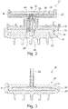
- figure 1 represents an exploded view of a voltage converter 10 comprising electronic power modules 12, in this example there are three, a support 14 of the electronic modules, an electrical connector 16, an electronic control card 18, and a support 20 of electronic card.
- the voltage converter 10 is an AC-DC converter.
- the voltage converter 10 is integrated in the housing of the electric machine.
- the electronic control board 18 is in particular intended to control the electronic power modules 12.
- the electronic board 18 is intended to be electrically connected with the power electronic modules 12 via at least one electrical connection element 22.
- the electrical connector 16 is arranged between the electronic power modules 12 and the support 20 of the electronic card.
- the electrical connector 16 is configured to electrically connect the electronic modules 12 to at least one of the electrical elements (phase ⁇ ), of the electrical machine and / or to at least one of the electrical elements (B + , B - ) of a source of electrical energy.
- the electrical elements of the electrical machine are, for example, phases ⁇ .
- the electrical elements of the electrical energy source are for example a positive DC terminal B + , a negative DC terminal B - or ground.
- the electrical connector 16 comprises orifices 24 arranged to allow access of the electrical connection elements 22 of the electronic modules 12 with the electronic control board 18.
- the support 14 of the electronic power unit is advantageously a housing comprising at least one open cavity 26 having a bottom on which the power electronic modules 12 are mounted.
- the housing allows thermal and electrical conduction, in particular for the recovery of mass and thermal diffusion.
- the open cavity 26 is intended to be filled with an insulating material so that the power electronic modules 12 are embedded in the insulating material. In particular, this configuration allows efficient isolation of the electronic modules 12.
- the power module support 14 is a heat sink, also called heat sink.
- the power modules 12 are attached to the heat sink to allow heat transfer between the power modules 12 and a cooling circuit (not shown), in order to dissipate the heat generated by the electronic modules 12.
- the support 20 of the electronic control board is arranged between the electronic power modules 12 and the electronic control board 18.
- the support 20 of the electronic control board is preferably made of insulating material, for example molded plastic.
- the support 20 comprises an open cavity 28 having a bottom 30 on which the electronic card 18 is intended to be received.
- the support 20 also comprises at least one hollow column 32 in which the at least one electrical connection element 22 of the electronic card 18 with the electronic modules 12 is intended to be inserted.
- the hollow column 32 in particular visible on the figure 2 extends from the open cavity 28 and is configured to communicate with the open cavity 28 at a first end 34 of the hollow column 32.
- the support 20 of the electronic card 18 comprises three hollow columns, each hollow column being intended to receive the electrical connection elements 22 of each electronic module 12 with the electronic control board 18.
- the open cavity 28 is intended to be filled with an insulating material so that the electronic control board 18 is embedded in the insulating material. The control electronic card 18 is thus effectively isolated.
- control electronic card support 20 may comprise a filling element 38 of the hollow column 32.
- the filling element 38 also called filling channel, may have a general shape of ramp, preferably a helical shape.
- One end of the filling element 38 communicates with the bottom 30 of the open cavity 28 and another end of the filling element 38 communicates with a side wall of the hollow column 32.
- a second end 36 of the hollow column 32 is in contact with the insulating material in which the electronic module 12 is embedded. This configuration makes it possible to guarantee the filling of the hollow column 32 of insulating material, and thus to ensure effective insulation of the electrical connection elements 22.
- the control electronic card 18 may advantageously comprise an orifice 48 arranged opposite the end of the channel 38 communicating with the bottom 30 of the open cavity 28.
- the orifice 48 of the electronic card 18 allows in particular the filling of the hollow column 32 of insulating material B via the channel 38.
- the section of the guide holes 46 opposite the electronic module 12 is larger than the section of the guide orifices 46 facing the electronic card 18.
- the two guide elements 44 have a circular section and comprise a frustoconical portion followed by a cylindrical portion.
- the electrical device 10 is intended to receive insulating materials A, B allowing isolation of the electronic power unit 12, the electronic control unit 18 and the electrical connection elements 22.
- the materials insulators A, B provide insulation against dust, liquids, gases or moisture.
- the insulating material may be a resin, such as an epoxy resin, or an insulating gel, such as a silicone gel.
- the electronic units 12, 18 of the electrical device 10 may be insulated with the same or different insulating materials A, B.
- the electronic control and power units are insulated with an identical insulating material, in particular with an insulating gel.
- the first and second zones are each in contact with the third zone so that the electrical device 10 comprises at least one space extending around the third zone and between the first and the second zone.
- the method of assembling the electrical device comprises a step S11 in which a support 14 of the electronic power unit, here an electronic power module 12 is provided.
- a support 14 of the electronic power unit here an electronic power module 12 is provided.
- the open cavity 26 of the support 14 is intended to receive an electronic power module 12 and to be filled with insulating material A, so that the electronic power unit 12 is embedded in the insulating material A.
- the assembly method of the electrical device may comprise a step S12 in which an electrical connector 16 is provided.
- the arrangement of the electrical connector 16 vis-à-vis an electronic module 12 and the support 14 of the electronic module is for example visible on the figure 4 .
- the electrical connector 16 is included at least in part in the space extending around the third zone and between the first and the second zone.
- the electrical connector 16 comprises an orifice 24 arranged to allow access of the electrical connection elements 22 of the electronic modules 12 with the electronic control board 18.
- the assembly method of the electrical device preferably comprises a step S13 in which a support 20 of the electronic control unit 18 as described above is provided.
- the support 20 of the electronic control unit is then arranged between the electronic power unit 12 and the electronic control unit 18.
- the electronic card support 20 is fixed in the support 14 of electronic modules so as to be opposite the electronic power modules 12.
- the support 20 preferably comprises an open cavity 28 intended to receive the electronic unit 18 and a hollow column 32 as previously described.
- the assembly method of the electrical device may comprise a step S15 for guiding the at least one electrical connection element 22.
- the electronic card support 20 comprises guiding elements 44 of the electrical connection elements 22 as represented on the figure 4 .
- the electrical connection elements are guided towards the electronic control unit 18 by the guide elements 44 arranged at the first end 34 of the hollow column 32.
- the assembly method of the electrical device according to the invention further comprises a step S20 of connecting the at least one electrical connection element 22. As shown in FIG. figure 4 one end of the electrical connection elements 22 is connected to the electronic module 12 and the opposite end to the end connected to said electronic power module 12 is connected to the electronic control board 18.
- step S30 can comprise a step S31 for filling the hollow column 32, in which the hollow column 32 is filled with insulating material B before drowning the electronic control unit 18 in the insulating material B.
- the deposition of insulating material B inside the hollow column 32 is performed by the filling element 38 of the electronic card support 20.
- the filling of the hollow column 32 by the filling element 38 makes it possible to completely fill the hollow column 32. This allows for better insulation of the electrical connection elements 22 and to avoid any risk of short circuiting at the level of the interconnection of the electronic module 12 with the electronic card 18.
- steps S11 to S15 can be performed consecutively and in combination before step S20.
- steps S11 to S15 can be performed consecutively or not, alone or in any combination possible.
- the electrical device for controlling an electric machine has been described in the context of a voltage converter for supplying an electric machine, in particular intended to power a motor vehicle.
- the invention is not limited to the embodiment described and illustrated, which has been given by way of example. On the contrary, other applications of the electrical device according to the invention are also possible without departing from the scope of the invention.
Abstract
L'invention concerne un dispositif électrique (10), notamment destiné à contrôler une machine électrique, comprenant : - une première zone remplie d'un matériau isolant (A) et comprenant une première unité électronique (12) noyée dans le matériau isolant (A) ; - une deuxième zone remplie d'un matériau isolant (B) et comprenant une seconde unité électronique (18) noyée dans le matériau isolant (B) ; et - une troisième zone remplie d'un matériau isolant (B) et comprenant au moins un élément de connexion électrique (22) noyé dans le matériau isolant (B), le au moins un élément de connexion électrique (22) connectant la première unité électronique (12) avec la seconde unité électronique (18) ; dans lequel la première et la deuxième zone sont chacune en contact avec la troisième zone de sorte que le dispositif électrique comprend au moins un espace s'étendant autour de la troisième zone et entre la première et la deuxième zone.The invention relates to an electrical device (10), in particular for controlling an electric machine, comprising: a first zone filled with an insulating material (A) and comprising a first electronic unit (12) embedded in the insulating material (A); a second zone filled with an insulating material (B) and comprising a second electronic unit (18) embedded in the insulating material (B); and a third zone filled with an insulating material (B) and comprising at least one electrical connection element embedded in the insulating material (B), the at least one electrical connection element connecting the first electronic unit (12) with the second electronic unit (18); wherein the first and second areas are each in contact with the third area so that the electrical device comprises at least one space extending around the third area and between the first and second areas.
Description
L'invention a pour objet un dispositif électrique destiné à contrôler une machine électrique et un procédé d'assemblage d'un tel dispositif électrique.The invention relates to an electrical device for controlling an electrical machine and a method of assembling such an electrical device.
Usuellement, un dispositif électrique destiné à contrôler une machine électrique, tel qu'un convertisseur de tension, comprend des unités électroniques qui nécessitent une isolation efficace à la poussière, aux liquides, aux gaz ou encore à l'humidité. Pour cela, une isolation à l'aide d'un dépôt de matériau isolant peut être réalisée.Usually, an electrical device for controlling an electrical machine, such as a voltage converter, includes electronic units that require effective isolation from dust, liquids, gases, or moisture. For this, insulation with a deposit of insulating material can be achieved.
Cependant, en général, l'isolation d'un dispositif électrique nécessite une quantité importante de matériau isolant afin de garantir une isolation efficace du dispositif électrique. De ce fait, ces dispositifs électriques ont des coûts de production élevés.However, in general, the isolation of an electrical device requires a large amount of insulating material to ensure effective isolation of the electrical device. As a result, these electrical devices have high production costs.
La présente invention vise à remédier à ces inconvénients en proposant un dispositif électrique permettant de réduire la quantité de matériau isolant nécessaire pour isoler le dispositif électrique, tout en garantissant une isolation efficace dudit dispositif électrique.The present invention aims to overcome these disadvantages by providing an electrical device to reduce the amount of insulating material necessary to isolate the electrical device, while ensuring effective insulation of said electrical device.
A cet effet, l'invention a pour objet un dispositif électrique, notamment destiné à contrôler une machine électrique, comprenant :
- une première zone remplie d'un matériau isolant et comprenant une première unité électronique, notamment une unité électronique de puissance, noyée dans le matériau isolant ;
- une deuxième zone remplie d'un matériau isolant et comprenant une seconde unité électronique, notamment une unité électronique de contrôle, noyée dans le matériau isolant ; et
- une troisième zone remplie d'un matériau isolant et comprenant au moins un élément de connexion électrique noyé dans le matériau isolant, le au moins un élément de connexion électrique connectant la première unité électronique avec la seconde unité électronique ;
- a first zone filled with an insulating material and comprising a first electronic unit, in particular an electronic power unit, embedded in the insulating material;
- a second zone filled with an insulating material and comprising a second electronic unit, in particular an electronic control unit, embedded in the insulating material; and
- a third zone filled with an insulating material and comprising at least one electrical connection element embedded in the insulating material, the at least one electrical connection element connecting the first electronic unit with the second electronic unit;
En particulier, l'espace est libre de matière, notamment dépourvu de matériau isolant.In particular, the space is free of material, in particular devoid of insulating material.
En particulier, l'électronique de puissance est destinée à délivrer un courant électrique à une machine électrique à partir d'une source de tension.In particular, the power electronics is intended to deliver an electric current to an electrical machine from a voltage source.
Avantageusement, dans le dispositif électrique selon l'invention, l'espace entre la première et la deuxième zone permet de diminuer les coûts de production d'un tel dispositif électrique, grâce à une réduction de la quantité de matériau isolant nécessaire pour isoler efficacement les unités électroniques de contrôle et de puissance. En outre, cet espace permet une circulation de l'air entre la première et la deuxième zone et autour de la troisième zone, et ainsi un meilleur refroidissement du dispositif électrique par convection.Advantageously, in the electrical device according to the invention, the space between the first and the second zone makes it possible to reduce the production costs of such an electrical device, by reducing the amount of insulating material necessary to effectively isolate the electronic control and power units. In addition, this space allows air circulation between the first and the second zone and around the third zone, and thus a better cooling of the electrical device by convection.
Le dispositif électrique selon l'invention peut également comprendre une ou plusieurs des caractéristiques suivantes, considérées individuellement ou selon toutes les combinaisons possibles :
- les première, deuxième et troisième zones sont superposées, les première et deuxième zones s'étendant sensiblement suivant des plans parallèles ;
- la troisième zone est définie au moins en partie par une colonne creuse dans laquelle le au moins un élément de connexion électrique est destiné à être inséré, la colonne creuse s'étendant entre la première et la deuxième zone ;
- la colonne creuse est remplie de matériau isolant ;
- le dispositif électrique selon l'invention comprend également un support d'une unité électronique agencé entre la première unité électronique et la seconde unité électronique et comprenant une cavité ouverte destinée à recevoir la seconde unité électronique ;
- la colonne creuse s'étend depuis la cavité ouverte, et est configurée pour communiquer avec la cavité ouverte à une première extrémité de la colonne creuse ;
- une seconde extrémité de la colonne creuse opposée à la première extrémité est en contact avec le matériau isolant dans lequel la première unité électronique est noyée ;
- le fond de la cavité ouverte comprend des éléments de guidage du au moins un élément de connexion électrique destinés à guider le au moins un élément de connexion électrique vers la seconde unité électronique, les éléments de guidage étant notamment agencés à la première extrémité de la colonne creuse ;
- le dispositif électrique selon l'invention comprend également un connecteur électrique configuré pour connecter électriquement la première unité électronique à au moins un des éléments électriques (phase ϕ, B+, B-) d'une machine électrique contrôlée par le dispositif électrique et/ou d'une source d'énergie électrique, et compris au moins en partie dans ledit espace s'étendant autour de la troisième zone et entre la première et la deuxième zone ;
- le connecteur électrique est agencé entre la première unité électronique et le support de la seconde unité électronique, le connecteur électrique comportant un orifice dans lequel la colonne creuse est destinée à être insérée.
- the first, second and third zones are superimposed, the first and second zones extending substantially in parallel planes;
- the third zone is defined at least in part by a hollow column in which the at least one electrical connection element is intended to be inserted, the hollow column extending between the first and the second zone;
- the hollow column is filled with insulating material;
- the electrical device according to the invention also comprises a support of an electronic unit arranged between the first electronic unit and the second electronic unit and comprising an open cavity intended to receive the second electronic unit;
- the hollow column extends from the open cavity, and is configured to communicate with the open cavity at a first end of the hollow column;
- a second end of the hollow column opposite the first end is in contact with the insulating material in which the first electronic unit is embedded;
- the bottom of the open cavity comprises guide elements of the at least one electrical connection element intended to guide the at least one electrical connection element towards the second electronic unit, the guide elements being in particular arranged at the first end of the column dig ;
- the electrical device according to the invention also comprises an electrical connector configured to electrically connect the first electronic unit to at least one of the electrical elements (phase φ, B + , B - ) of an electrical machine controlled by the electrical device and / or a source of electrical energy, and at least partially understood in said space extending around the third zone and between the first and second zones;
- the electrical connector is arranged between the first electronic unit and the support of the second electronic unit, the electrical connector having an orifice in which the hollow column is intended to be inserted.
L'invention se rapporte également à un procédé d'assemblage d'un dispositif électrique, notamment destiné à contrôler une machine électrique, comprenant :
- une étape dans laquelle une première unité électronique, notamment une unité électronique de puissance, noyée dans un matériau isolant formant une première zone, une seconde unité électronique, notamment une unité électronique de contrôle, et au moins un élément de connexion électrique dont une extrémité est connectée à ladite première unité électronique sont fournis ;
- une étape de connexion du au moins un élément de connexion électrique, dans laquelle une extrémité opposée à l'extrémité connectée à ladite première unité électronique est connectée à la seconde unité électronique; et
- une étape de dépôt d'un matériau isolant, dans laquelle la seconde unité électronique est noyée dans un matériau isolant formant une deuxième zone et le au moins un élément de connexion électrique est noyé dans un matériau isolant formant une troisième zone de sorte que la première et la deuxième zone sont chacune en contact avec la troisième zone et que le dispositif électrique comprend au moins un espace s'étendant autour de la troisième zone et entre la première et la deuxième zone.
- a step in which a first electronic unit, in particular an electronic power unit, embedded in an insulating material forming a first zone, a second electronic unit, in particular an electronic control unit, and at least one electrical connection element whose one end is connected to said first electronic unit are provided;
- a step of connecting the at least one electrical connection member, wherein an end opposite the end connected to said first electronic unit is connected to the second electronic unit; and
- a step of depositing an insulating material, wherein the second electronic unit is embedded in an insulating material forming a second zone and the at least one electrical connection element is embedded in an insulating material forming a third zone so that the first and the second zone are each in contact with the third zone and the electrical device comprises at least one space extending around the third zone and between the first and the second zone.
Autrement dit, une droite passant par la première zone, ledit espace et la deuxième zone, comprend une partie incluse dans la première zone, une partie incluse dans ledit espace et une partie incluse dans la deuxième zone, lesdites parties étant contigües.In other words, a straight line passing through the first zone, said space and the second zone comprises a portion included in the first zone, a portion included in said space and a portion included in the second zone, said portions being contiguous.
En particulier, l'espace est libre de matière, notamment dépourvu de matériau isolant.In particular, the space is free of material, in particular devoid of insulating material.
En particulier, l'électronique de puissance est destinée à délivrer un courant électrique à une machine électrique à partir d'une source de tension. Par exemple, la machine électrique est un démarreur, un alterno-démarreur ou une autre machine électrique embarquée dans le véhiculeIn particular, the power electronics is intended to deliver an electric current to an electrical machine from a voltage source. For example, the electric machine is a starter, an alternator-starter or another electrical machine embedded in the vehicle
Avantageusement, le procédé d'assemblage du dispositif électrique permet une isolation efficace des unités électroniques, tout en garantissant une réduction des coûts de production, notamment grâce à une réduction de la quantité de matériau nécessaire pour l'isolation du dispositif électrique. En outre, l'espace s'étendant autour de la troisième zone et entre la première et la deuxième zone permet une circulation de l'air entre la première et la deuxième zone et autour de la troisième zone, et ainsi un meilleur refroidissement du dispositif électrique par convection.Advantageously, the assembly method of the electrical device allows effective isolation of the electronic units, while ensuring a reduction in production costs, in particular by reducing the amount of material necessary for the isolation of the electrical device. In addition, the space extending around the third zone and between the first and the second zone allows air circulation between the first and second zones and around the third zone, and thus better cooling of the device. electric convection.
Le procédé d'assemblage d'un dispositif électrique selon l'invention peut également comprendre une ou plusieurs des caractéristiques suivantes, considérées individuellement ou selon toutes les combinaisons possibles :
- le procédé d'assemblage d'un dispositif électrique selon l'invention comprend en outre, avant l'étape de connexion du au moins un élément de connexion électrique :
- une étape dans laquelle un support d'une unité électronique est fourni, le support de l'unité électronique étant agencé entre la première unité électronique et la seconde unité électronique, et comprenant une cavité ouverte destinée à recevoir la seconde unité électronique, et une colonne creuse s'étendant depuis la cavité ouverte, et communiquant avec la cavité ouverte à une première extrémité de la colonne creuse ;
- une étape d'insertion du au moins un élément de connexion électrique dans la colonne creuse, dans laquelle le au moins un élément de connexion électrique est inséré dans la colonne creuse en vue de sa connexion avec la seconde unité électronique, de sorte qu'une seconde extrémité de la colonne creuse opposée à la première extrémité est en contact avec le matériau isolant dans lequel la première unité électronique est noyée ;
- le procédé d'assemblage d'un dispositif électrique selon l'invention comprend une étape de guidage du au moins un élément de connexion électrique, dans laquelle le au moins un élément de connexion électrique est guidé vers la seconde unité électronique en vue de sa connexion avec la seconde unité électronique par des éléments de guidage agencés à la première extrémité de la colonne creuse ;
- l'étape de dépôt de matériau isolant comprend une étape de remplissage de la colonne creuse, dans laquelle la colonne creuse est remplie de matériau isolant avant de noyer la seconde unité électronique dans le matériau isolant.
- the method of assembling an electrical device according to the invention further comprises, before the step of connecting the at least one electrical connection element:
- a step in which a support of an electronic unit is provided, the support of the electronic unit being arranged between the first electronic unit and the second electronic unit, and comprising an open cavity for receiving the second electronic unit, and a column hollow extending from the open cavity, and communicating with the open cavity at a first end of the hollow column;
- a step of inserting the at least one electrical connection element into the hollow column, wherein the at least one electrical connection element is inserted into the hollow column for connection with the second electronic unit, so that a second end of the hollow column opposite the first end is in contact with the insulating material in which the first electronic unit is embedded;
- the method of assembling an electrical device according to the invention comprises a step of guiding the at least one electrical connection element, in which the at least one electrical connection element is guided towards the second electronic unit with a view to its connection with the second electronic unit by guiding elements arranged at the first end of the hollow column;
- the step of depositing insulating material comprises a step of filling the hollow column, wherein the hollow column is filled with insulating material before embedding the second electronic unit in the insulating material.
D'autres caractéristiques et avantages de la présente invention apparaitront à la lecture de la description et des figures suivantes :
- la
figure 1 est une vue éclatée selon un mode de réalisation préféré d'un dispositif électrique selon l'invention, - la
figure 2 représente une vue en coupe d'un dispositif électrique selon le mode de réalisation préféré de lafigure 1 , - les
figures 3 et4 représentent une vue en coupe du dispositif électrique de lafigure 1 à différentes étapes du procédé d'assemblage dudit dispositif électrique, et - la
figure 5 est un organigramme des étapes du procédé d'assemblage du dispositif électrique selon un mode de réalisation préféré de l'invention.
- the
figure 1 is an exploded view according to a preferred embodiment of an electrical device according to the invention, - the
figure 2 represents a sectional view of an electrical device according to the preferred embodiment of thefigure 1 , - the
figures 3 and4 represent a sectional view of the electrical device of thefigure 1 at different stages of the assembly process of said electrical device, and - the
figure 5 is a flowchart of the steps of the assembly method of the electrical device according to a preferred embodiment of the invention.
Il est à noter que ces dessins n'ont d'autre but que d'illustrer le texte de la description et ne constituent en aucune sorte une limitation de la portée de l'invention.It should be noted that these drawings have no other purpose than to illustrate the text of the description and do not constitute in any way a limitation of the scope of the invention.
Sur les différentes figures, les éléments analogues sont désignés par des références identiques.In the various figures, the analogous elements are designated by identical references.
Le dispositif électrique selon l'invention est par exemple destiné à contrôler une machine électrique, notamment une machine électrique destinée à être intégrée dans un véhicule automobile, telle qu'une machine électrique tournante.The electrical device according to the invention is for example intended to control an electric machine, in particular an electric machine intended to be integrated in a motor vehicle, such as a rotating electrical machine.
Le dispositif électrique comprend au moins une première unité électronique, par exemple une unité électronique de puissance, au moins une seconde unité électronique, par exemple une unité électronique de contrôle, et au moins un élément de connexion électrique destiné à connecter électriquement lesdites unités électroniques.The electrical device comprises at least a first electronic unit, for example an electronic power unit, at least a second electronic unit, for example an electronic control unit, and at least one electrical connection element for electrically connecting said electronic units.
Le dispositif électrique est par exemple un convertisseur de tension tel qu'illustré sur les figures. Bien entendu, l'invention n'est nullement limitée à un convertisseur de tension, mais au contraire le dispositif électrique pourrait être tout autre dispositif électrique destiné à contrôler une machine électrique.The electrical device is for example a voltage converter as shown in the figures. Of course, the invention is not limited to a voltage converter, but on the contrary the electrical device could be any other electrical device for controlling an electric machine.
De même, la première unité électronique sera illustrée par une unité électronique de puissance, telle que un ou plusieurs modules électroniques de puissance et la seconde unité électronique sera illustrée par une unité électronique de contrôle, telle qu'une carte électronique de contrôle. Bien entendu, les unités électroniques pourraient être respectivement tout autre composant électronique.Similarly, the first electronic unit will be illustrated by an electronic power unit, such as one or more electronic power modules and the second electronic unit will be illustrated by an electronic control unit, such as an electronic control board. Of course, the electronic units could be respectively any other electronic component.
En particulier, la
Avantageusement, le convertisseur de tension 10 est un convertisseur alternatif-continu. De préférence, le convertisseur de tension 10 est intégré au carter de la machine électrique.Advantageously, the
La carte électronique de contrôle 18 est notamment destinée à contrôler les modules électroniques de puissance 12. En particulier, la carte électronique 18 est destinée à être connectée électriquement avec les modules électroniques de puissance 12 via au moins un élément de connexion électrique 22.The
Le connecteur électrique 16 est agencé entre les modules électroniques de puissance 12 et le support 20 de la carte électronique. Le connecteur électrique 16 est configuré pour connecter électriquement les modules électroniques 12 à au moins un des éléments électriques (phase ϕ), de la machine électrique et/ou à au moins un des éléments électriques (B+, B-) d'une source d'énergie électrique. Les éléments électriques de la machine électrique sont, par exemple, des phases ϕ. Les éléments électriques de la source d'énergie électrique sont par exemple une borne continue positive B+, une borne continue négative B- ou la masse. Il y a de préférence un module électronique de puissance 12 par phase ϕ. En outre, comme représenté sur la
Le support 14 de l'unité électronique de puissance est avantageusement un boitier comprenant au moins une cavité ouverte 26 ayant un fond sur lequel les modules électroniques de puissance 12 sont montés. De façon avantageuse, le boitier permet une conduction thermique et électrique, notamment pour la reprise de la masse et la diffusion thermique. La cavité ouverte 26 est destinée à être remplie d'un matériau isolant de sorte que les modules électroniques de puissance 12 sont noyés dans le matériau isolant. En particulier, cette configuration permet une isolation efficace des modules électroniques 12. De façon avantageuse, le support 14 de module puissance est un dissipateur de chaleur, aussi nommé dissipateur thermique. Les modules de puissance 12 sont fixés au dissipateur thermique afin de permettre le transfert thermique entre les modules de puissance 12 et un circuit de refroidissement (non représenté), afin de dissiper la chaleur générée par les modules électroniques 12. En outre, la cavité ouverte 26 de réception des modules électroniques peut comprendre des éléments de positionnement (non représentés) destinés à positionner les modules électroniques 12 sur le support 14 dans une position prédéterminée. Ces éléments de positionnement permettent de faciliter et garantir un positionnement correct et rapide des modules électroniques 12 sur le support 14 en vue de leur connexion électrique avec la carte électronique 18.The
Le support 20 de la carte électronique de contrôle est agencé entre les modules électroniques de puissance 12 et la carte électronique de contrôle 18. Le support 20 de la carte électronique de contrôle est de préférence en matière isolante, par exemple moulé en matière plastique.The
Le support 20 comprend une cavité ouverte 28 ayant un fond 30 sur lequel la carte électronique 18 est destinée à être reçue.The
Le support 20 comprend également au moins une colonne creuse 32 dans laquelle le au moins un élément de connexion électrique 22 de la carte électronique 18 avec les modules électroniques 12 est destiné à être inséré. La colonne creuse 32, notamment visible sur la
Avantageusement, le support 20 de carte électronique de contrôle peut comprendre un élément de remplissage 38 de la colonne creuse 32. L'élément de remplissage 38, également appelé canal de remplissage, peut avoir une forme générale de rampe, préférentiellement une forme hélicoïdale. Une extrémité de l'élément de remplissage 38 communique avec le fond 30 de la cavité ouverte 28 et une autre extrémité de l'élément de remplissage 38 communique avec une paroi latérale de la colonne creuse 32. De préférence, une seconde extrémité 36 de la colonne creuse 32 est en contact avec le matériau isolant dans lequel le module électronique 12 est noyé. Cette configuration permet de garantir le remplissage de la colonne creuse 32 de matériau isolant, et ainsi d'assurer une isolation efficace des éléments de connexion électrique 22.Advantageously, the control
La carte électronique de contrôle 18 peut comprendre avantageusement un orifice 48 agencé en vis-à-vis de l'extrémité du canal 38 communiquant avec le fond 30 de la cavité ouverte 28. L'orifice 48 de la carte électronique 18 permet notamment le remplissage de la colonne creuse 32 de matériau isolant B par l'intermédiaire du canal 38.The control
En outre, le fond 30 de la cavité ouverte 28 comprend de préférence des éléments de positionnement 40 destinés à positionner la carte électronique 18 sur le support 20 dans une position prédéterminée. Autrement dit, les éléments de positionnement 40 disposés sur le support 20 de la carte électronique sont destinés à coopérer avec des éléments de positionnement complémentaires 42 de la carte électronique 18. Par exemple, sur la
De plus, le fond 30 de la cavité ouverte 28 comprend avantageusement des éléments de guidage 44 du au moins un élément de connexion électrique 22 agencés à la première extrémité 34 de la colonne creuse 32 et destinés à guider le au moins un élément de connexion électrique 22 vers la carte électronique 18. Par exemple, sur la
De plus, le dispositif électrique 10 est destiné à recevoir des matériaux isolants A, B permettant une isolation de l'unité électronique de puissance 12, de l'unité électronique de contrôle 18 et des éléments de connexion électrique 22. Les matériaux isolants A, B permettent une isolation à la poussière, aux liquides, aux gaz ou encore à l'humidité.In addition, the
Par exemple, le matériau isolant peut être une résine, telle qu'une résine époxy, ou un gel isolant, tel qu'un gel de silicone.For example, the insulating material may be a resin, such as an epoxy resin, or an insulating gel, such as a silicone gel.
Les unités électroniques 12, 18 du dispositif électrique 10 peuvent être isolées avec des matériaux isolants A, B identiques ou différents. De préférence les unités électroniques de contrôle et de puissance sont isolées avec un matériau isolant identique, notamment avec un gel isolant.The
Plus précisément, le dispositif électrique comprend :
- une première zone remplie d'un matériau isolant A et comprenant une unité électronique de puissance 12 noyée dans le matériau isolant ;
- une deuxième zone remplie d'un matériau isolant B et comprenant une unité électronique de contrôle 18 noyée dans le matériau isolant B ; et
- une troisième zone remplie d'un matériau isolant B et comprenant au moins un élément de connexion électrique 22 noyé dans le matériau isolant B.
- a first zone filled with an insulating material A and comprising an
electronic power unit 12 embedded in the insulating material; - a second zone filled with an insulating material B and comprising an
electronic control unit 18 embedded in the insulating material B; and - a third zone filled with an insulating material B and comprising at least one
electrical connection element 22 embedded in the insulating material B.
La première et la deuxième zone sont chacune en contact avec la troisième zone de sorte que le dispositif électrique 10 comprend au moins un espace s'étendant autour de la troisième zone et entre la première et la deuxième zone.The first and second zones are each in contact with the third zone so that the
Plus précisément, comme représenté sur la
Autrement dit, le matériau isolant A, B emplit l'espace intérieur libre de chaque cavité ouverte 26, 28 autour des composants de la carte électronique 18 et/ou des modules électroniques de puissance 12. Le matériau isolant A, B permet l'étanchéité de la carte électronique 18 et des modules électroniques de puissance 12, notamment l'étanchéité à la poussière et aux liquides. Le matériau isolant permet ainsi de supprimer tout risque de court-circuit possible au niveau de la carte électronique 18 ou des modules de puissance 12.In other words, the insulating material A, B fills the free internal space of each
De plus, comme représenté sur la
En outre, l'espace compris entre la carte électronique 18 et le module de puissance 12 et entourant la colonne creuse 32 est dépourvu de matière, notamment de matériau isolant. L'espace libre de matière, notamment de matériau isolant, entre la première et la deuxième zone a, entre autres, pour effet de laisser un espace libre pour la circulation d'air, permettant ainsi un refroidissement par convection. De plus, cette configuration permet de diminuer les coûts de production du dispositif électrique 10, grâce notamment à un gain en matériau isolant.In addition, the space between the
De plus, l'invention concerne également un procédé d'assemblage d'un tel dispositif électrique selon l'invention. Différentes étapes du procédé d'assemblage sont illustrées sur les
En regard de la
Par exemple et de préférence, le procédé d'assemblage du dispositif électrique comprend une étape S11 dans laquelle un support 14 de l'unité électronique de puissance, ici un module électronique de puissance 12 est fourni. Comme représenté sur la
Avantageusement, le procédé d'assemblage du dispositif électrique peut comprendre une étape S12 dans laquelle un connecteur électrique 16 est fourni. L'agencement du connecteur électrique 16 vis-à-vis d'un module électronique 12 et du support 14 de module électronique est par exemple visible sur la
Selon un mode de réalisation préféré illustré en
Ainsi, les première, deuxième et troisième zones sont superposées, les première et deuxième zones s'étendant sensiblement suivant des plans parallèles.Thus, the first, second and third zones are superimposed, the first and second zones extending substantially in parallel planes.
Suite à l'étape S13, le procédé d'assemblage peut comprendre une étape S14 d'insertion du au moins un élément de connexion électrique 22 dans la colonne creuse 32. Comme représenté sur la
De manière avantageuse, le procédé d'assemblage du dispositif électrique peut comprendre une étape S15 de guidage du au moins un élément de connexion électrique 22. Le support 20 de carte électronique comprend des éléments de guidage 44 des éléments de connexion électrique 22 tels que représentés sur la
Le procédé d'assemblage du dispositif électrique selon l'invention comprend en outre une étape S20 de connexion du au moins un élément de connexion électrique 22. Comme représenté sur la
Suite à l'étape S20, le procédé d'assemblage du dispositif électrique selon l'invention comprend une étape S30 de dépôt d'un matériau isolant. Comme illustré sur la
D'autre part, l'étape S30 peut comprendre une étape S31 de remplissage de la colonne creuse 32, dans laquelle la colonne creuse 32 est remplie de matériau isolant B avant de noyer l'unité électronique de contrôle 18 dans le matériau isolant B. Le dépôt de matériau isolant B à l'intérieur de la colonne creuse 32 est effectué par l'élément de remplissage 38 du support 20 de carte électronique. Le remplissage de la colonne creuse 32 par l'élément de remplissage 38 permet de remplir entièrement la colonne creuse 32. Cela permet une meilleure isolation des éléments de connexion électrique 22 et d'éviter d'éventuels risques de court-circuit au niveau de l'interconnexion du module électronique 12 avec la carte électronique 18.On the other hand, step S30 can comprise a step S31 for filling the
Comme illustré sur la figure 6, selon un mode de réalisation préféré de l'invention, les étapes S11 à S15 peuvent être réalisées consécutivement et en combinaison avant l'étape S20. Bien entendu, ce mode de réalisation n'est pas limitatif, les étapes S11 à S15 peuvent être réalisées consécutivement ou non, seules ou selon toute combinaison possible.As illustrated in FIG. 6, according to a preferred embodiment of the invention, steps S11 to S15 can be performed consecutively and in combination before step S20. Of course, this embodiment is not limiting, the steps S11 to S15 can be performed consecutively or not, alone or in any combination possible.
Le dispositif électrique destiné à contrôler une machine électrique a été décrit dans le cadre d'un convertisseur de tension destiné à alimenter une machine électrique notamment destinée à alimenter un véhicule automobile. Bien entendu, l'invention n'est nullement limitée au mode de réalisation décrit et illustré, qui n'a été donné qu'à titre d'exemple. Au contraire, d'autres applications du dispositif électrique conforme à l'invention sont également possibles sans sortir du cadre de l'invention.The electrical device for controlling an electric machine has been described in the context of a voltage converter for supplying an electric machine, in particular intended to power a motor vehicle. Of course, the invention is not limited to the embodiment described and illustrated, which has been given by way of example. On the contrary, other applications of the electrical device according to the invention are also possible without departing from the scope of the invention.
Claims (14)
Applications Claiming Priority (1)
| Application Number | Priority Date | Filing Date | Title |
|---|---|---|---|
| FR1561738A FR3044864B1 (en) | 2015-12-02 | 2015-12-02 | ELECTRIC DEVICE AND METHOD FOR ASSEMBLING SUCH AN ELECTRICAL DEVICE |
Publications (2)
| Publication Number | Publication Date |
|---|---|
| EP3177121A1 true EP3177121A1 (en) | 2017-06-07 |
| EP3177121B1 EP3177121B1 (en) | 2021-03-24 |
Family
ID=55589962
Family Applications (1)
| Application Number | Title | Priority Date | Filing Date |
|---|---|---|---|
| EP16201059.9A Active EP3177121B1 (en) | 2015-12-02 | 2016-11-29 | Electric device and method for assembling such an electric device |
Country Status (5)
| Country | Link |
|---|---|
| US (2) | US10230288B2 (en) |
| EP (1) | EP3177121B1 (en) |
| JP (1) | JP6914642B2 (en) |
| CN (1) | CN107516979B (en) |
| FR (1) | FR3044864B1 (en) |
Cited By (1)
| Publication number | Priority date | Publication date | Assignee | Title |
|---|---|---|---|---|
| FR3080317A1 (en) * | 2018-04-19 | 2019-10-25 | Compagnie Plastic Omnium | METHOD FOR MANUFACTURING BODY COMPONENT ELEMENT HAVING AN IMPROVED DEFROSTING SYSTEM |
Families Citing this family (3)
| Publication number | Priority date | Publication date | Assignee | Title |
|---|---|---|---|---|
| JP7043338B2 (en) * | 2017-05-26 | 2022-03-29 | ミネベアミツミ株式会社 | Centrifugal fan |
| EP3434250A1 (en) * | 2017-07-25 | 2019-01-30 | Sensorial Processing Technology Barcelona, SL | System and method for distributed sensorial stimulation |
| US11417953B2 (en) * | 2019-11-14 | 2022-08-16 | Plume Design, Inc. | Electronic shielding of antennas from fan controls in a compact electronic device |
Citations (6)
| Publication number | Priority date | Publication date | Assignee | Title |
|---|---|---|---|---|
| US5657203A (en) * | 1991-05-31 | 1997-08-12 | Nippondenso Co., Ltd. | Electronic device having a plurality of circuit boards arranged therein |
| US20090086455A1 (en) * | 2007-09-27 | 2009-04-02 | Sanyo Electric Co., Ltd. | Circuit device and method of manufacturing the same |
| US20090103276A1 (en) * | 2007-09-27 | 2009-04-23 | Sanyo Electric Co., Ltd. | Circuit device and method of manufacturing the same |
| DE102007062918A1 (en) * | 2007-12-21 | 2009-06-25 | Endress + Hauser Gmbh + Co. Kg | Method for casting printed circuit board, involves forming plug connection in between space of socket and connector depending on design of casting mold cap and cover |
| WO2015033062A2 (en) * | 2013-09-09 | 2015-03-12 | Valeo Equipements Electriques Moteur | Electronic assembly for a rotary electric machine for a motor vehicle |
| US20150092376A1 (en) * | 2013-09-30 | 2015-04-02 | Infineon Technologies Ag | Power Semiconductor Module and Method for Producing a Power Semiconductor Module |
Family Cites Families (51)
| Publication number | Priority date | Publication date | Assignee | Title |
|---|---|---|---|---|
| UA32456C2 (en) * | 1996-01-25 | 2000-12-15 | Сіменс Аг | РПаЎ±б |
| EP0884781A3 (en) * | 1997-06-12 | 1999-06-30 | Hitachi, Ltd. | Power semiconductor module |
| DE69819284T2 (en) * | 1997-11-25 | 2004-07-29 | Sumitomo Wiring Systems, Ltd., Yokkaichi | Electrical connector unit |
| JP3674333B2 (en) * | 1998-09-11 | 2005-07-20 | 株式会社日立製作所 | Power semiconductor module and electric motor drive system using the same |
| JP4234259B2 (en) * | 1999-05-14 | 2009-03-04 | 富士通テン株式会社 | Combination structure of electronic equipment |
| JP3886295B2 (en) * | 1999-06-15 | 2007-02-28 | 松下冷機株式会社 | Power control device and compressor for refrigeration system |
| JP2001267714A (en) * | 2000-03-16 | 2001-09-28 | Sony Corp | Electronic circuit device |
| JP2002058134A (en) * | 2000-08-09 | 2002-02-22 | Auto Network Gijutsu Kenkyusho:Kk | Installation structure for electric control unit |
| KR100576902B1 (en) * | 2000-10-02 | 2006-05-03 | 마츠시타 덴끼 산교 가부시키가이샤 | Card type recording medium and production method therefor |
| JP2003100937A (en) * | 2001-09-26 | 2003-04-04 | Hitachi Ltd | High-frequency module |
| JP3861669B2 (en) * | 2001-11-22 | 2006-12-20 | ソニー株式会社 | Manufacturing method of multichip circuit module |
| US6922332B2 (en) * | 2002-04-10 | 2005-07-26 | Furukawa Electric Co., Ltd. | Electric connection box |
| US7354318B2 (en) * | 2002-09-19 | 2008-04-08 | The Furukawa Electric Co., Ltd. | Joint connector |
| US7547975B2 (en) * | 2003-07-30 | 2009-06-16 | Tdk Corporation | Module with embedded semiconductor IC and method of fabricating the module |
| KR100585226B1 (en) * | 2004-03-10 | 2006-06-01 | 삼성전자주식회사 | Semiconductor package having heat spreader and stack package using the same |
| WO2006035528A1 (en) * | 2004-09-29 | 2006-04-06 | Murata Manufacturing Co., Ltd. | Stack module and method for manufacturing the same |
| US7332808B2 (en) * | 2005-03-30 | 2008-02-19 | Sanyo Electric Co., Ltd. | Semiconductor module and method of manufacturing the same |
| JP2006287101A (en) * | 2005-04-04 | 2006-10-19 | Toyota Motor Corp | Power module and its manufacturing method |
| JP4520355B2 (en) * | 2005-04-19 | 2010-08-04 | パナソニック株式会社 | Semiconductor module |
| JP2006324568A (en) * | 2005-05-20 | 2006-11-30 | Matsushita Electric Ind Co Ltd | Multilayer module and its manufacturing method |
| JP2007123314A (en) * | 2005-10-25 | 2007-05-17 | Yazaki Corp | Relay module and electrical equipment unit |
| JP4462193B2 (en) * | 2006-01-13 | 2010-05-12 | ソニー株式会社 | Semiconductor device, semiconductor device inspection method, and semiconductor device inspection device |
| JP2008085089A (en) * | 2006-09-28 | 2008-04-10 | Matsushita Electric Ind Co Ltd | Resin wiring board and semiconductor device |
| JP4423285B2 (en) * | 2006-12-19 | 2010-03-03 | 新光電気工業株式会社 | Electronic component built-in substrate and method for manufacturing electronic component built-in substrate |
| JP4965989B2 (en) * | 2006-12-19 | 2012-07-04 | 新光電気工業株式会社 | Electronic component built-in substrate and method for manufacturing electronic component built-in substrate |
| JP4926692B2 (en) * | 2006-12-27 | 2012-05-09 | 新光電気工業株式会社 | WIRING BOARD, MANUFACTURING METHOD THEREOF, AND SEMICONDUCTOR DEVICE |
| JP4278680B2 (en) * | 2006-12-27 | 2009-06-17 | 三菱電機株式会社 | Electronic control unit |
| US8253033B2 (en) * | 2007-09-03 | 2012-08-28 | Panasonic Corporation | Circuit board with connection layer with fillet |
| JP2009064916A (en) * | 2007-09-05 | 2009-03-26 | Kokusan Denki Co Ltd | Electronic unit, and manufacturing method of the same |
| JP5147344B2 (en) * | 2007-09-27 | 2013-02-20 | オンセミコンダクター・トレーディング・リミテッド | Circuit device and manufacturing method thereof |
| JP5319908B2 (en) * | 2007-10-31 | 2013-10-16 | セミコンダクター・コンポーネンツ・インダストリーズ・リミテッド・ライアビリティ・カンパニー | Circuit equipment |
| JP2009081325A (en) * | 2007-09-27 | 2009-04-16 | Sanyo Electric Co Ltd | Circuit device |
| TW200915970A (en) * | 2007-09-27 | 2009-04-01 | Sanyo Electric Co | Circuit device, circuit module and outdoor equipment |
| JP2009141169A (en) * | 2007-12-07 | 2009-06-25 | Shinko Electric Ind Co Ltd | Semiconductor device |
| JP5265183B2 (en) * | 2007-12-14 | 2013-08-14 | 新光電気工業株式会社 | Semiconductor device |
| US7727022B2 (en) * | 2008-02-14 | 2010-06-01 | Delphi Technologies, Inc. | On harness PCB electrical center |
| US8027168B2 (en) * | 2008-08-13 | 2011-09-27 | Delphi Technologies, Inc. | Electrical center with vertical power bus bar |
| JP5100694B2 (en) * | 2009-04-01 | 2012-12-19 | 三菱電機株式会社 | Semiconductor device |
| JP5454681B2 (en) * | 2010-05-26 | 2014-03-26 | 株式会社村田製作所 | Module substrate and manufacturing method thereof |
| JP5692588B2 (en) * | 2010-12-28 | 2015-04-01 | 株式会社デンソー | Drive device |
| JP2013103535A (en) * | 2011-11-10 | 2013-05-30 | Honda Elesys Co Ltd | Electronic control unit for electric power steering |
| JP5812428B2 (en) * | 2012-03-09 | 2015-11-11 | 住友電装株式会社 | Electrical junction box |
| ES2638857T3 (en) * | 2012-03-28 | 2017-10-24 | Abb Research Ltd. | Heat exchanger for traction converters |
| JP5640036B2 (en) * | 2012-03-29 | 2014-12-10 | カヤバ工業株式会社 | Electronic board connection structure |
| US8961197B2 (en) * | 2012-06-08 | 2015-02-24 | Lear Corporation | Fuse housing assembly |
| JP5918664B2 (en) * | 2012-09-10 | 2016-05-18 | 株式会社東芝 | Manufacturing method of stacked semiconductor device |
| JP5861614B2 (en) * | 2012-11-12 | 2016-02-16 | 株式会社デンソー | High voltage electric device and electric compressor |
| JP5994609B2 (en) * | 2012-11-30 | 2016-09-21 | 矢崎総業株式会社 | Electrical junction box |
| US9196510B2 (en) * | 2013-11-12 | 2015-11-24 | Infineon Technologies Ag | Semiconductor package comprising two semiconductor modules and laterally extending connectors |
| US10242969B2 (en) * | 2013-11-12 | 2019-03-26 | Infineon Technologies Ag | Semiconductor package comprising a transistor chip module and a driver chip module and a method for fabricating the same |
| JP6438225B2 (en) * | 2014-07-24 | 2018-12-12 | 株式会社ジェイデバイス | Semiconductor package |
-
2015
- 2015-12-02 FR FR1561738A patent/FR3044864B1/en active Active
-
2016
- 2016-11-29 EP EP16201059.9A patent/EP3177121B1/en active Active
- 2016-11-30 US US15/364,331 patent/US10230288B2/en active Active
- 2016-12-01 JP JP2016234562A patent/JP6914642B2/en active Active
- 2016-12-02 CN CN201611273161.3A patent/CN107516979B/en active Active
-
2018
- 2018-09-21 US US16/138,222 patent/US10476357B2/en active Active
Patent Citations (6)
| Publication number | Priority date | Publication date | Assignee | Title |
|---|---|---|---|---|
| US5657203A (en) * | 1991-05-31 | 1997-08-12 | Nippondenso Co., Ltd. | Electronic device having a plurality of circuit boards arranged therein |
| US20090086455A1 (en) * | 2007-09-27 | 2009-04-02 | Sanyo Electric Co., Ltd. | Circuit device and method of manufacturing the same |
| US20090103276A1 (en) * | 2007-09-27 | 2009-04-23 | Sanyo Electric Co., Ltd. | Circuit device and method of manufacturing the same |
| DE102007062918A1 (en) * | 2007-12-21 | 2009-06-25 | Endress + Hauser Gmbh + Co. Kg | Method for casting printed circuit board, involves forming plug connection in between space of socket and connector depending on design of casting mold cap and cover |
| WO2015033062A2 (en) * | 2013-09-09 | 2015-03-12 | Valeo Equipements Electriques Moteur | Electronic assembly for a rotary electric machine for a motor vehicle |
| US20150092376A1 (en) * | 2013-09-30 | 2015-04-02 | Infineon Technologies Ag | Power Semiconductor Module and Method for Producing a Power Semiconductor Module |
Cited By (1)
| Publication number | Priority date | Publication date | Assignee | Title |
|---|---|---|---|---|
| FR3080317A1 (en) * | 2018-04-19 | 2019-10-25 | Compagnie Plastic Omnium | METHOD FOR MANUFACTURING BODY COMPONENT ELEMENT HAVING AN IMPROVED DEFROSTING SYSTEM |
Also Published As
| Publication number | Publication date |
|---|---|
| FR3044864B1 (en) | 2018-01-12 |
| FR3044864A1 (en) | 2017-06-09 |
| US20190020246A1 (en) | 2019-01-17 |
| JP2017135362A (en) | 2017-08-03 |
| CN107516979A (en) | 2017-12-26 |
| EP3177121B1 (en) | 2021-03-24 |
| US10476357B2 (en) | 2019-11-12 |
| US10230288B2 (en) | 2019-03-12 |
| JP6914642B2 (en) | 2021-08-04 |
| US20170163129A1 (en) | 2017-06-08 |
| CN107516979B (en) | 2020-04-21 |
Similar Documents
| Publication | Publication Date | Title |
|---|---|---|
| EP3176918B1 (en) | Electronic architecture intended for powering an electric machine for a motor vehicle | |
| EP3177121B1 (en) | Electric device and method for assembling such an electric device | |
| EP3177115B1 (en) | Assembly of an electronic power module and a support for an electronic power module, electronic architecture including same, voltage converter and electric machine comprising same | |
| EP3176919B1 (en) | Electrical connector intended for being electrically connected to a source of electrical power | |
| EP3177123B1 (en) | Mounting of an electronic card, assembly of an electronic card and such a mounting, voltage converter comprising same, and electric machine for motor vehicle comprising same | |
| FR3030917A1 (en) | ||
| FR2855332A1 (en) | Serial advanced technology attachment connector for connecting external hard drive to notebook computer motherboard, has signal and power panels disposed in insulation housing of notebook computer | |
| FR3007218A1 (en) | ELECTRICAL CONNECTION DEVICE FOR COMPRESSOR AND COMPRESSOR COMPRISING SUCH AN ELECTRICAL CONNECTION DEVICE | |
| EP3621093A1 (en) | Capacitive block comprising a heat sink | |
| EP3177122B1 (en) | Mounting for an electronic unit, electrical device comprising same, and electric machine comprising said electrical device | |
| FR3120745A1 (en) | Gasket for a plug-in electrical device as well as a plug-in electrical device and a plug-in electrical connection assembly with such a gasket | |
| EP3314682B1 (en) | Electric energy storage module | |
| FR2997797A1 (en) | Assembly for electric compressor utilized for liquid refrigerant e.g. R134a circuit in electric car, has sealing unit insulating electric connection element of wall separating motor from control device on level of connection opening | |
| FR3044841A1 (en) | ELECTRICAL CONNECTOR FOR CONNECTING ELECTRICALLY TO AT LEAST ONE ELECTRONIC UNIT AND TO AN ELECTRIC POWER SOURCE | |
| FR2907266A1 (en) | ELECTRICAL CONNECTION DEVICE, IN PARTICULAR FOR ELECTRICAL SOLAR PANEL | |
| EP2536261A1 (en) | Electronic power module with integrated capacitance | |
| WO2004010539A1 (en) | Electrical connector, in particular for vehicle heating device | |
| EP3476665B1 (en) | Electrical insulation bar, in particular for a power electronics module of an inverter | |
| FR3044837A1 (en) | ELECTRICAL CONNECTOR FOR CONNECTING ELECTRICALLY TO AT LEAST ONE ELECTRONIC UNIT AND TO AN ELECTRIC POWER SOURCE | |
| WO2020201543A1 (en) | Capacitive block comprising a frame of electrically insulating material | |
| FR3044839A1 (en) | ELECTRICAL CONNECTOR FOR CONNECTING AN ELECTRICAL DEVICE WITH AN ELECTRICAL MACHINE CONTROLLED THEREBY | |
| FR3078591A1 (en) | CHARGING SOCKET AND METHOD FOR MOUNTING SUCH SOCKET ON AN ELECTRIC CABLE | |
| FR3073117B1 (en) | HEATING UNIT COMPRISING A SEALING ELEMENT | |
| FR2928784A1 (en) | Electric connection device for electric solar panel, has printed circuit board carrying electronic components such as diodes, where board is connected electrically on connection elements that are forcibly connected with conductors | |
| FR2549646A1 (en) | Connector element having a double sealing barrier and connector using the said element. |
Legal Events
| Date | Code | Title | Description |
|---|---|---|---|
| STAA | Information on the status of an ep patent application or granted ep patent |
Free format text: STATUS: EXAMINATION IS IN PROGRESS |
|
| 17P | Request for examination filed |
Effective date: 20161129 |
|
| AK | Designated contracting states |
Kind code of ref document: A1 Designated state(s): AL AT BE BG CH CY CZ DE DK EE ES FI FR GB GR HR HU IE IS IT LI LT LU LV MC MK MT NL NO PL PT RO RS SE SI SK SM TR |
|
| AX | Request for extension of the european patent |
Extension state: BA ME |
|
| PUAI | Public reference made under article 153(3) epc to a published international application that has entered the european phase |
Free format text: ORIGINAL CODE: 0009012 |
|
| GRAP | Despatch of communication of intention to grant a patent |
Free format text: ORIGINAL CODE: EPIDOSNIGR1 |
|
| STAA | Information on the status of an ep patent application or granted ep patent |
Free format text: STATUS: GRANT OF PATENT IS INTENDED |
|
| INTG | Intention to grant announced |
Effective date: 20201015 |
|
| GRAS | Grant fee paid |
Free format text: ORIGINAL CODE: EPIDOSNIGR3 |
|
| GRAA | (expected) grant |
Free format text: ORIGINAL CODE: 0009210 |
|
| STAA | Information on the status of an ep patent application or granted ep patent |
Free format text: STATUS: THE PATENT HAS BEEN GRANTED |
|
| AK | Designated contracting states |
Kind code of ref document: B1 Designated state(s): AL AT BE BG CH CY CZ DE DK EE ES FI FR GB GR HR HU IE IS IT LI LT LU LV MC MK MT NL NO PL PT RO RS SE SI SK SM TR |
|
| REG | Reference to a national code |
Ref country code: GB Ref legal event code: FG4D Free format text: NOT ENGLISH |
|
| REG | Reference to a national code |
Ref country code: CH Ref legal event code: EP |
|
| REG | Reference to a national code |
Ref country code: IE Ref legal event code: FG4D Free format text: LANGUAGE OF EP DOCUMENT: FRENCH |
|
| REG | Reference to a national code |
Ref country code: AT Ref legal event code: REF Ref document number: 1375852 Country of ref document: AT Kind code of ref document: T Effective date: 20210415 Ref country code: DE Ref legal event code: R096 Ref document number: 602016054741 Country of ref document: DE |
|
| REG | Reference to a national code |
Ref country code: LT Ref legal event code: MG9D |
|
| PG25 | Lapsed in a contracting state [announced via postgrant information from national office to epo] |
Ref country code: HR Free format text: LAPSE BECAUSE OF FAILURE TO SUBMIT A TRANSLATION OF THE DESCRIPTION OR TO PAY THE FEE WITHIN THE PRESCRIBED TIME-LIMIT Effective date: 20210324 Ref country code: FI Free format text: LAPSE BECAUSE OF FAILURE TO SUBMIT A TRANSLATION OF THE DESCRIPTION OR TO PAY THE FEE WITHIN THE PRESCRIBED TIME-LIMIT Effective date: 20210324 Ref country code: GR Free format text: LAPSE BECAUSE OF FAILURE TO SUBMIT A TRANSLATION OF THE DESCRIPTION OR TO PAY THE FEE WITHIN THE PRESCRIBED TIME-LIMIT Effective date: 20210625 Ref country code: NO Free format text: LAPSE BECAUSE OF FAILURE TO SUBMIT A TRANSLATION OF THE DESCRIPTION OR TO PAY THE FEE WITHIN THE PRESCRIBED TIME-LIMIT Effective date: 20210624 Ref country code: BG Free format text: LAPSE BECAUSE OF FAILURE TO SUBMIT A TRANSLATION OF THE DESCRIPTION OR TO PAY THE FEE WITHIN THE PRESCRIBED TIME-LIMIT Effective date: 20210624 |
|
| PG25 | Lapsed in a contracting state [announced via postgrant information from national office to epo] |
Ref country code: RS Free format text: LAPSE BECAUSE OF FAILURE TO SUBMIT A TRANSLATION OF THE DESCRIPTION OR TO PAY THE FEE WITHIN THE PRESCRIBED TIME-LIMIT Effective date: 20210324 Ref country code: LV Free format text: LAPSE BECAUSE OF FAILURE TO SUBMIT A TRANSLATION OF THE DESCRIPTION OR TO PAY THE FEE WITHIN THE PRESCRIBED TIME-LIMIT Effective date: 20210324 Ref country code: SE Free format text: LAPSE BECAUSE OF FAILURE TO SUBMIT A TRANSLATION OF THE DESCRIPTION OR TO PAY THE FEE WITHIN THE PRESCRIBED TIME-LIMIT Effective date: 20210324 |
|
| REG | Reference to a national code |
Ref country code: NL Ref legal event code: MP Effective date: 20210324 |
|
| REG | Reference to a national code |
Ref country code: AT Ref legal event code: MK05 Ref document number: 1375852 Country of ref document: AT Kind code of ref document: T Effective date: 20210324 |
|
| PG25 | Lapsed in a contracting state [announced via postgrant information from national office to epo] |
Ref country code: NL Free format text: LAPSE BECAUSE OF FAILURE TO SUBMIT A TRANSLATION OF THE DESCRIPTION OR TO PAY THE FEE WITHIN THE PRESCRIBED TIME-LIMIT Effective date: 20210324 |
|
| PG25 | Lapsed in a contracting state [announced via postgrant information from national office to epo] |
Ref country code: SM Free format text: LAPSE BECAUSE OF FAILURE TO SUBMIT A TRANSLATION OF THE DESCRIPTION OR TO PAY THE FEE WITHIN THE PRESCRIBED TIME-LIMIT Effective date: 20210324 Ref country code: AT Free format text: LAPSE BECAUSE OF FAILURE TO SUBMIT A TRANSLATION OF THE DESCRIPTION OR TO PAY THE FEE WITHIN THE PRESCRIBED TIME-LIMIT Effective date: 20210324 Ref country code: LT Free format text: LAPSE BECAUSE OF FAILURE TO SUBMIT A TRANSLATION OF THE DESCRIPTION OR TO PAY THE FEE WITHIN THE PRESCRIBED TIME-LIMIT Effective date: 20210324 Ref country code: EE Free format text: LAPSE BECAUSE OF FAILURE TO SUBMIT A TRANSLATION OF THE DESCRIPTION OR TO PAY THE FEE WITHIN THE PRESCRIBED TIME-LIMIT Effective date: 20210324 Ref country code: CZ Free format text: LAPSE BECAUSE OF FAILURE TO SUBMIT A TRANSLATION OF THE DESCRIPTION OR TO PAY THE FEE WITHIN THE PRESCRIBED TIME-LIMIT Effective date: 20210324 |
|
| PG25 | Lapsed in a contracting state [announced via postgrant information from national office to epo] |
Ref country code: RO Free format text: LAPSE BECAUSE OF FAILURE TO SUBMIT A TRANSLATION OF THE DESCRIPTION OR TO PAY THE FEE WITHIN THE PRESCRIBED TIME-LIMIT Effective date: 20210324 Ref country code: SK Free format text: LAPSE BECAUSE OF FAILURE TO SUBMIT A TRANSLATION OF THE DESCRIPTION OR TO PAY THE FEE WITHIN THE PRESCRIBED TIME-LIMIT Effective date: 20210324 Ref country code: PT Free format text: LAPSE BECAUSE OF FAILURE TO SUBMIT A TRANSLATION OF THE DESCRIPTION OR TO PAY THE FEE WITHIN THE PRESCRIBED TIME-LIMIT Effective date: 20210726 Ref country code: PL Free format text: LAPSE BECAUSE OF FAILURE TO SUBMIT A TRANSLATION OF THE DESCRIPTION OR TO PAY THE FEE WITHIN THE PRESCRIBED TIME-LIMIT Effective date: 20210324 Ref country code: IS Free format text: LAPSE BECAUSE OF FAILURE TO SUBMIT A TRANSLATION OF THE DESCRIPTION OR TO PAY THE FEE WITHIN THE PRESCRIBED TIME-LIMIT Effective date: 20210724 |
|
| REG | Reference to a national code |
Ref country code: DE Ref legal event code: R097 Ref document number: 602016054741 Country of ref document: DE |
|
| PG25 | Lapsed in a contracting state [announced via postgrant information from national office to epo] |
Ref country code: AL Free format text: LAPSE BECAUSE OF FAILURE TO SUBMIT A TRANSLATION OF THE DESCRIPTION OR TO PAY THE FEE WITHIN THE PRESCRIBED TIME-LIMIT Effective date: 20210324 Ref country code: ES Free format text: LAPSE BECAUSE OF FAILURE TO SUBMIT A TRANSLATION OF THE DESCRIPTION OR TO PAY THE FEE WITHIN THE PRESCRIBED TIME-LIMIT Effective date: 20210324 Ref country code: DK Free format text: LAPSE BECAUSE OF FAILURE TO SUBMIT A TRANSLATION OF THE DESCRIPTION OR TO PAY THE FEE WITHIN THE PRESCRIBED TIME-LIMIT Effective date: 20210324 |
|
| PLBE | No opposition filed within time limit |
Free format text: ORIGINAL CODE: 0009261 |
|
| STAA | Information on the status of an ep patent application or granted ep patent |
Free format text: STATUS: NO OPPOSITION FILED WITHIN TIME LIMIT |
|
| PG25 | Lapsed in a contracting state [announced via postgrant information from national office to epo] |
Ref country code: SI Free format text: LAPSE BECAUSE OF FAILURE TO SUBMIT A TRANSLATION OF THE DESCRIPTION OR TO PAY THE FEE WITHIN THE PRESCRIBED TIME-LIMIT Effective date: 20210324 |
|
| 26N | No opposition filed |
Effective date: 20220104 |
|
| PG25 | Lapsed in a contracting state [announced via postgrant information from national office to epo] |
Ref country code: IS Free format text: LAPSE BECAUSE OF FAILURE TO SUBMIT A TRANSLATION OF THE DESCRIPTION OR TO PAY THE FEE WITHIN THE PRESCRIBED TIME-LIMIT Effective date: 20210724 |
|
| PG25 | Lapsed in a contracting state [announced via postgrant information from national office to epo] |
Ref country code: MC Free format text: LAPSE BECAUSE OF FAILURE TO SUBMIT A TRANSLATION OF THE DESCRIPTION OR TO PAY THE FEE WITHIN THE PRESCRIBED TIME-LIMIT Effective date: 20210324 |
|
| REG | Reference to a national code |
Ref country code: CH Ref legal event code: PL |
|
| GBPC | Gb: european patent ceased through non-payment of renewal fee |
Effective date: 20211129 |
|
| PG25 | Lapsed in a contracting state [announced via postgrant information from national office to epo] |
Ref country code: LU Free format text: LAPSE BECAUSE OF NON-PAYMENT OF DUE FEES Effective date: 20211129 Ref country code: BE Free format text: LAPSE BECAUSE OF NON-PAYMENT OF DUE FEES Effective date: 20211130 |
|
| REG | Reference to a national code |
Ref country code: BE Ref legal event code: MM Effective date: 20211130 |
|
| PG25 | Lapsed in a contracting state [announced via postgrant information from national office to epo] |
Ref country code: LI Free format text: LAPSE BECAUSE OF NON-PAYMENT OF DUE FEES Effective date: 20211130 Ref country code: CH Free format text: LAPSE BECAUSE OF NON-PAYMENT OF DUE FEES Effective date: 20211130 |
|
| PG25 | Lapsed in a contracting state [announced via postgrant information from national office to epo] |
Ref country code: IE Free format text: LAPSE BECAUSE OF NON-PAYMENT OF DUE FEES Effective date: 20211129 Ref country code: GB Free format text: LAPSE BECAUSE OF NON-PAYMENT OF DUE FEES Effective date: 20211129 |
|
| PG25 | Lapsed in a contracting state [announced via postgrant information from national office to epo] |
Ref country code: IT Free format text: LAPSE BECAUSE OF FAILURE TO SUBMIT A TRANSLATION OF THE DESCRIPTION OR TO PAY THE FEE WITHIN THE PRESCRIBED TIME-LIMIT Effective date: 20210324 |
|
| PG25 | Lapsed in a contracting state [announced via postgrant information from national office to epo] |
Ref country code: HU Free format text: LAPSE BECAUSE OF FAILURE TO SUBMIT A TRANSLATION OF THE DESCRIPTION OR TO PAY THE FEE WITHIN THE PRESCRIBED TIME-LIMIT; INVALID AB INITIO Effective date: 20161129 |
|
| PG25 | Lapsed in a contracting state [announced via postgrant information from national office to epo] |
Ref country code: CY Free format text: LAPSE BECAUSE OF FAILURE TO SUBMIT A TRANSLATION OF THE DESCRIPTION OR TO PAY THE FEE WITHIN THE PRESCRIBED TIME-LIMIT Effective date: 20210324 |
|
| P01 | Opt-out of the competence of the unified patent court (upc) registered |
Effective date: 20230528 |
|
| PGFP | Annual fee paid to national office [announced via postgrant information from national office to epo] |
Ref country code: FR Payment date: 20231124 Year of fee payment: 8 Ref country code: DE Payment date: 20231107 Year of fee payment: 8 |