EP3177004A2 - Imaging device, imaging system, and method for driving imaging device - Google Patents
Imaging device, imaging system, and method for driving imaging device Download PDFInfo
- Publication number
- EP3177004A2 EP3177004A2 EP16201760.2A EP16201760A EP3177004A2 EP 3177004 A2 EP3177004 A2 EP 3177004A2 EP 16201760 A EP16201760 A EP 16201760A EP 3177004 A2 EP3177004 A2 EP 3177004A2
- Authority
- EP
- European Patent Office
- Prior art keywords
- electric charges
- transfer switch
- holding means
- pixels
- transfer
- Prior art date
- Legal status (The legal status is an assumption and is not a legal conclusion. Google has not performed a legal analysis and makes no representation as to the accuracy of the status listed.)
- Granted
Links
Images



Classifications
-
- H—ELECTRICITY
- H04—ELECTRIC COMMUNICATION TECHNIQUE
- H04N—PICTORIAL COMMUNICATION, e.g. TELEVISION
- H04N25/00—Circuitry of solid-state image sensors [SSIS]; Control thereof
- H04N25/50—Control of the SSIS exposure
- H04N25/53—Control of the integration time
- H04N25/533—Control of the integration time by using differing integration times for different sensor regions
- H04N25/534—Control of the integration time by using differing integration times for different sensor regions depending on the spectral component
-
- H—ELECTRICITY
- H10—SEMICONDUCTOR DEVICES; ELECTRIC SOLID-STATE DEVICES NOT OTHERWISE PROVIDED FOR
- H10F—INORGANIC SEMICONDUCTOR DEVICES SENSITIVE TO INFRARED RADIATION, LIGHT, ELECTROMAGNETIC RADIATION OF SHORTER WAVELENGTH OR CORPUSCULAR RADIATION
- H10F39/00—Integrated devices, or assemblies of multiple devices, comprising at least one element covered by group H10F30/00, e.g. radiation detectors comprising photodiode arrays
- H10F39/80—Constructional details of image sensors
- H10F39/803—Pixels having integrated switching, control, storage or amplification elements
-
- H—ELECTRICITY
- H04—ELECTRIC COMMUNICATION TECHNIQUE
- H04N—PICTORIAL COMMUNICATION, e.g. TELEVISION
- H04N23/00—Cameras or camera modules comprising electronic image sensors; Control thereof
- H04N23/70—Circuitry for compensating brightness variation in the scene
- H04N23/745—Detection of flicker frequency or suppression of flicker wherein the flicker is caused by illumination, e.g. due to fluorescent tube illumination or pulsed LED illumination
-
- H—ELECTRICITY
- H04—ELECTRIC COMMUNICATION TECHNIQUE
- H04N—PICTORIAL COMMUNICATION, e.g. TELEVISION
- H04N25/00—Circuitry of solid-state image sensors [SSIS]; Control thereof
- H04N25/50—Control of the SSIS exposure
- H04N25/53—Control of the integration time
- H04N25/531—Control of the integration time by controlling rolling shutters in CMOS SSIS
-
- H—ELECTRICITY
- H04—ELECTRIC COMMUNICATION TECHNIQUE
- H04N—PICTORIAL COMMUNICATION, e.g. TELEVISION
- H04N25/00—Circuitry of solid-state image sensors [SSIS]; Control thereof
- H04N25/50—Control of the SSIS exposure
- H04N25/53—Control of the integration time
- H04N25/532—Control of the integration time by controlling global shutters in CMOS SSIS
-
- H—ELECTRICITY
- H04—ELECTRIC COMMUNICATION TECHNIQUE
- H04N—PICTORIAL COMMUNICATION, e.g. TELEVISION
- H04N25/00—Circuitry of solid-state image sensors [SSIS]; Control thereof
- H04N25/50—Control of the SSIS exposure
- H04N25/53—Control of the integration time
- H04N25/533—Control of the integration time by using differing integration times for different sensor regions
-
- H—ELECTRICITY
- H04—ELECTRIC COMMUNICATION TECHNIQUE
- H04N—PICTORIAL COMMUNICATION, e.g. TELEVISION
- H04N25/00—Circuitry of solid-state image sensors [SSIS]; Control thereof
- H04N25/50—Control of the SSIS exposure
- H04N25/57—Control of the dynamic range
- H04N25/58—Control of the dynamic range involving two or more exposures
-
- H—ELECTRICITY
- H04—ELECTRIC COMMUNICATION TECHNIQUE
- H04N—PICTORIAL COMMUNICATION, e.g. TELEVISION
- H04N25/00—Circuitry of solid-state image sensors [SSIS]; Control thereof
- H04N25/50—Control of the SSIS exposure
- H04N25/57—Control of the dynamic range
- H04N25/58—Control of the dynamic range involving two or more exposures
- H04N25/587—Control of the dynamic range involving two or more exposures acquired sequentially, e.g. using the combination of odd and even image fields
- H04N25/589—Control of the dynamic range involving two or more exposures acquired sequentially, e.g. using the combination of odd and even image fields with different integration times, e.g. short and long exposures
-
- H—ELECTRICITY
- H04—ELECTRIC COMMUNICATION TECHNIQUE
- H04N—PICTORIAL COMMUNICATION, e.g. TELEVISION
- H04N25/00—Circuitry of solid-state image sensors [SSIS]; Control thereof
- H04N25/70—SSIS architectures; Circuits associated therewith
-
- H—ELECTRICITY
- H04—ELECTRIC COMMUNICATION TECHNIQUE
- H04N—PICTORIAL COMMUNICATION, e.g. TELEVISION
- H04N25/00—Circuitry of solid-state image sensors [SSIS]; Control thereof
- H04N25/70—SSIS architectures; Circuits associated therewith
- H04N25/76—Addressed sensors, e.g. MOS or CMOS sensors
- H04N25/77—Pixel circuitry, e.g. memories, A/D converters, pixel amplifiers, shared circuits or shared components
-
- H—ELECTRICITY
- H04—ELECTRIC COMMUNICATION TECHNIQUE
- H04N—PICTORIAL COMMUNICATION, e.g. TELEVISION
- H04N25/00—Circuitry of solid-state image sensors [SSIS]; Control thereof
- H04N25/70—SSIS architectures; Circuits associated therewith
- H04N25/76—Addressed sensors, e.g. MOS or CMOS sensors
- H04N25/77—Pixel circuitry, e.g. memories, A/D converters, pixel amplifiers, shared circuits or shared components
- H04N25/771—Pixel circuitry, e.g. memories, A/D converters, pixel amplifiers, shared circuits or shared components comprising storage means other than floating diffusion
-
- H—ELECTRICITY
- H04—ELECTRIC COMMUNICATION TECHNIQUE
- H04N—PICTORIAL COMMUNICATION, e.g. TELEVISION
- H04N25/00—Circuitry of solid-state image sensors [SSIS]; Control thereof
- H04N25/70—SSIS architectures; Circuits associated therewith
- H04N25/76—Addressed sensors, e.g. MOS or CMOS sensors
- H04N25/78—Readout circuits for addressed sensors, e.g. output amplifiers or A/D converters
-
- H—ELECTRICITY
- H10—SEMICONDUCTOR DEVICES; ELECTRIC SOLID-STATE DEVICES NOT OTHERWISE PROVIDED FOR
- H10F—INORGANIC SEMICONDUCTOR DEVICES SENSITIVE TO INFRARED RADIATION, LIGHT, ELECTROMAGNETIC RADIATION OF SHORTER WAVELENGTH OR CORPUSCULAR RADIATION
- H10F39/00—Integrated devices, or assemblies of multiple devices, comprising at least one element covered by group H10F30/00, e.g. radiation detectors comprising photodiode arrays
- H10F39/10—Integrated devices
- H10F39/12—Image sensors
- H10F39/18—Complementary metal-oxide-semiconductor [CMOS] image sensors; Photodiode array image sensors
- H10F39/186—Complementary metal-oxide-semiconductor [CMOS] image sensors; Photodiode array image sensors having arrangements for blooming suppression
- H10F39/1865—Overflow drain structures
-
- H—ELECTRICITY
- H10—SEMICONDUCTOR DEVICES; ELECTRIC SOLID-STATE DEVICES NOT OTHERWISE PROVIDED FOR
- H10F—INORGANIC SEMICONDUCTOR DEVICES SENSITIVE TO INFRARED RADIATION, LIGHT, ELECTROMAGNETIC RADIATION OF SHORTER WAVELENGTH OR CORPUSCULAR RADIATION
- H10F39/00—Integrated devices, or assemblies of multiple devices, comprising at least one element covered by group H10F30/00, e.g. radiation detectors comprising photodiode arrays
- H10F39/80—Constructional details of image sensors
- H10F39/803—Pixels having integrated switching, control, storage or amplification elements
- H10F39/8033—Photosensitive area
-
- H—ELECTRICITY
- H10—SEMICONDUCTOR DEVICES; ELECTRIC SOLID-STATE DEVICES NOT OTHERWISE PROVIDED FOR
- H10F—INORGANIC SEMICONDUCTOR DEVICES SENSITIVE TO INFRARED RADIATION, LIGHT, ELECTROMAGNETIC RADIATION OF SHORTER WAVELENGTH OR CORPUSCULAR RADIATION
- H10F39/00—Integrated devices, or assemblies of multiple devices, comprising at least one element covered by group H10F30/00, e.g. radiation detectors comprising photodiode arrays
- H10F39/80—Constructional details of image sensors
- H10F39/803—Pixels having integrated switching, control, storage or amplification elements
- H10F39/8037—Pixels having integrated switching, control, storage or amplification elements the integrated elements comprising a transistor
-
- H—ELECTRICITY
- H04—ELECTRIC COMMUNICATION TECHNIQUE
- H04N—PICTORIAL COMMUNICATION, e.g. TELEVISION
- H04N23/00—Cameras or camera modules comprising electronic image sensors; Control thereof
- H04N23/56—Cameras or camera modules comprising electronic image sensors; Control thereof provided with illuminating means
Definitions
- the present invention relates to an imaging device, an imaging system, and a method for driving the imaging device.
- CMOS Complementary Metal Oxide Semiconductor
- LED light emitting diode
- fluorescent light sources used for traffic signals and electric bulletin boards appear to be lighting up with constant brightness to human eyes
- these light sources are actually blinking at high frequencies in synchronization with the frequency of a commercial power supply.
- DC direct current
- the luminance is controlled based on a pulse-driven method such as Pulse Width Modulation (PWM) to restrain the current consumption and control the brightness.
- PWM Pulse Width Modulation
- a still image may be captured as if the light source is not lighting up and a moving image may be captured as if the light source is frequently blinking because of varying luminance values of images between frames.
- a moving image may be captured as if the light source is frequently blinking because of varying luminance values of images between frames.
- the present invention is directed to an imaging device capable of capturing an image with the influence of the blinking state of a light source restrained while ensuring synchronicity of charge accumulation, and also to an imaging system and a method for driving the imaging device.
- an imaging device as specified in claims 1 to 13.
- an imaging system as specified in claim 14.
- a method for driving an imaging device as specified in clams 15 to 17.
- FIG. 1 A configuration of an imaging device according to a first embodiment of the present invention and a method for driving the imaging device will be described below with reference to Figs. 1 to 4 .
- FIG. 3 is an overall block diagram illustrating an imaging device according to the present embodiment.
- An imaging device 101 can be configured with one chip using a semiconductor substrate.
- the imaging device 101 includes a plurality of pixels arranged in an imaging region 102.
- the imaging device 101 also includes a control unit 103.
- the control unit 103 supplies control signals and power voltages to a vertical scanning unit 104, a signal processing unit 105, and an output unit 106.
- the vertical scanning unit 104 supplies drive signals to a plurality of pixels arranged in the imaging region 102.
- the vertical scanning unit 104 supplies drive signals to each pixel row or each set of a plurality of pixel rows.
- the vertical scanning unit 104 can be configured with shift registers or address decoders.
- the signal processing unit 105 includes column circuits, horizontal scanning circuits, and horizontal output lines. Each column circuit may include a plurality of circuit blocks. Circuit blocks include a signal holding unit, a column amplifier circuit, a noise removal unit, and an analog-to-digital (AD) conversion unit.
- the horizontal scanning circuit can be configured with shift registers or address decoders. An analog signal or a digital signal may be output to the horizontal output lines.
- the output unit 106 outputs signals transmitted via the horizontal output lines to the outside of the imaging device 101.
- the output unit 106 includes buffers or amplifier circuits.
- the vertical scanning unit 104, the signal processing unit 105, and the output unit 106 are arranged outside the imaging region 102.
- Fig. 4 illustrates an example of a configuration of equivalent circuits of pixel portions in the imaging region 102 according to the present embodiment.
- Fig. 4 illustrates four pixels 300 as an example.
- a pixel 300 includes a photoelectric conversion unit 301, a charge holding unit 302, a first transfer switch 304 (also referred to as "TX1"), and a second transfer switch 305 (also referred to as "TX2").
- the pixel 300 also includes an amplifying unit 310, a reset transistor 309, a selection transistor 307, and an input node 303.
- the photoelectric conversion unit 301 accumulates the electric charges generated by incident light.
- a photodiode for example, is used as the photoelectric conversion unit 301.
- the first transfer switch 304 transfers the electric charges generated by the photoelectric conversion unit 301 to the charge holding unit 302.
- the charge holding unit 302 holds the electric charges generated due to the incident light by the photoelectric conversion unit 301.
- the second transfer switch 305 transfers the electric charges held by the charge holding unit 302 to the input node 303 of the amplifying unit 310.
- Metal-Oxide Semiconductor (MOS) transistors for example, are used as the first transfer switch 304 and the second transfer switch 305.
- the operation of the first transfer switch 304 is controlled by control signals (drive pulses) supplied via a control line 321.
- the operation of the second transfer switch 305 is controlled by control signals supplied via a control line 322.
- the selection transistor 307 selects a pixel 300 that outputs a signal to an output line 308.
- the amplifying unit 310 of the selected pixel 300 outputs a signal based on the electric charges generated by the incident light to the output line 308.
- the amplifying unit 310 configures, for example, a source follower circuit.
- the reset transistor 309 resets the voltage of the input node 303 of the amplifying unit 310 to the potential of a reset line 326 by the signal of a control line 325.
- the pixel 300 includes a discharge switch 318 (also referred to as “Overflow Drain (OFD)").
- OFD Overflow Drain
- the discharge switch 318 discharges the electric charges of the photoelectric conversion unit 301 to the power supply node 324 such as an overflow drain, and resets the potential caused by the electric charges of the photoelectric conversion unit 301.
- the operation of the discharge switch 318 is controlled by control signals supplied via a control line 323.
- the start and the end of the charge accumulation time period can be synchronized between the photoelectric conversion units 301 of a plurality of pixels 300, thus ensuring synchronicity of charge accumulation.
- the charge accumulation time period can be started, for example, by controlling the discharge switches 318 of a plurality of pixels 300 from ON to OFF.
- the discharge switch 318 is not always necessary and a configuration called Vertical Overflow Drain may be employed in which the electric charges from the photoelectric conversion unit 301 are discharged to the semiconductor substrate.
- a switch (not illustrated) for resetting the potential of the charge holding unit 302 can also be separately provided. After turning the second transfer switch 305 OFF from ON and before transferring the electric charges from the photoelectric conversion unit 301 to the charge holding unit 302, this reset switch may be turned ON to reset the potential of the charge holding unit 302.
- Fig. 1 is a timing chart illustrating operations of the imaging device 101 according to the present embodiment.
- a waveform 201 schematically indicates a full-wave rectified waveform of an alternating current (AC) power supply.
- the AC power supply is a power supply having a frequency of, for example, 50 or 60 Hz.
- a time period T211 is equivalent to the cycle of the AC power supply, for example, 1/50 or 1/60 seconds.
- a waveform 202 indicates a lighting state of a light source using the power supply of the waveform 201.
- the H level indicates a turn-ON state and the L level indicates a turn-OFF state.
- Examples of light sources operating on an AC power supply include LED light sources used for traffic signals.
- a time period T212 indicates a blinking cycle of the light source, which is one half of the time period T211 that is the cycle of the AC power supply.
- a time period T213 indicates a turn-ON period of the light source, and a time period T214 indicates a turn-OFF period of the light source.
- a signal waveform 203 indicates a waveform of the pulse signal of the control line 323 of the discharge switch 318.
- the discharge switch 318 turns ON and the electric charges are discharged from the photoelectric conversion unit 301 to the power supply node 324.
- the signal waveform 203 changes from the H level to the L level and the discharge switch 318 changes from ON to OFF at the same timing for all pixels. Therefore, charge accumulation in the photoelectric conversion unit 301 is started at the same timing for all pixels.
- the same timing does not necessarily mean exact synchronicity but means substantially the same time.
- a signal waveform 204 indicates a waveform of the pulse signal of the control line 321 of the first transfer switch 304.
- this pulse signal changes from the L level to the H level
- the first transfer switch 304 changes from OFF to ON and the electric charges generated by the photoelectric conversion unit 301 are transferred to the charge holding unit 302.
- the signal waveform 204 changes from the L level to the H level for all pixels. Therefore, the electric charges generated by the photoelectric conversion unit 301 are simultaneously transferred to the charge holding unit 302 for all pixels, and the first charge accumulation is ended at the same timing for all pixels.
- a time period T215 indicates a time period (sampling period) from the start to the end of one charge accumulation.
- the present embodiment is characterized in short-time sampling performed a plurality of times. More specifically, for all pixels, when the first transfer switch 304 intermittently turns ON a plurality of times at the same timing, the electric charges are intermittently transferred from the photoelectric conversion unit 301 to the charge holding unit 302 a plurality of times. The operation of intermittently turning the discharge switch 318 ON and OFF is repeated so that the discharge switch 318 turns OFF for all pixels at the time when the first transfer switch 304 turns ON.
- a signal waveform 205 indicates a waveform of the pulse signal of the control line 322 of the second transfer switch 305.
- the second transfer switch 305 turns ON and the electric charges held by the charge holding unit 302 are transferred to the amplifying unit 310.
- Fig. 1 illustrates the signal waveforms 205 for controlling the second transfer switches 305 provided in the n-th to (n + x)-th rows.
- the pulse signal of the control line 322 of the second transfer switch 305 row-sequentially changes from the L level to the H level, and therefore the second transfer switch 305 also row-sequentially turns ON. Accordingly, the electric charges held on a row basis by the charge holding unit 302 are transferred to the amplifying unit 310.
- a time period T217 is a time period during which the electric charges are held by the charge holding unit 302 in the n-th row.
- the first transfer switch 304 intermittently turns ON a plurality of times while the second transfer switch 305 is maintained to OFF.
- the time period T217 is also a time period during which the photoelectric conversion unit 301 generates the electric charges to be held by the charge holding unit 302.
- the time period T217 is equivalent to a time period since the start of the first sampling operation until the end of the last sampling operation in sampling operations performed a plurality of times.
- signals generated with multi-exposure are accumulated by the charge holding unit 302 because of such control.
- the time period T218 indicates a time period since the start of the first sampling operation till the end of the last sampling operation in the (n + 1)-th row.
- the first transfer switch 304 since the first transfer switch 304 is controlled at the same timing for all pixels, the first transfer switches 304 of the pixel (first pixel) in the n-th row and the pixel (second pixel) in the (n + 1) -th row are controlled at the same timing.
- the second transfer switch 305 of the pixel (second pixel) in the (n + 1) -th row is controlled to ON in a state where the second transfer switch 305 of the pixel (first pixel) in the n-th row is maintained to OFF.
- charge transfer from the charge holding unit 302 to the amplifying unit 310 is row-sequentially performed.
- a time period T220 indicates one-frame period. During this period, an image for one frame is row-sequentially output from the charge holding unit 302 to the amplifying unit 310.
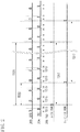
- Fig. 2 illustrates in detail a relationship between the signal waveforms 203, 204, and 205 out of the signals illustrated in Fig. 1 . These waveforms correspond to the discharge switch 318, the first transfer switch 304, and the second transfer switch 305, respectively.
- the time period T215 indicates one sampling period. This time period is equivalent to a time period since the time when the discharge switch 318 changes from ON to OFF till the time when the first transfer switch 304 changes from ON to OFF. At the time when the first transfer switch 304 turns ON a plurality of times, the discharge switch 318 is OFF.
- a time period T221 indicates one-frame period and is equivalent to a time period since the time when the second transfer switch 305 in the n-th row changes from OFF to ON till the time when the second transfer switch 305 in the n-th row changes from OFF to ON again.
- a time period T222 indicates a vertical scanning interval for each row and, for example, is equivalent to a time period since the time when the second transfer switch 305 of the pixel in the n-th row changes from OFF to ON till the time when the second transfer switch 305 of the pixel in the (n + 1)-th row changes from OFF to ON.
- the time period T215 may be, for example, a time period equal to or shorter than a half of the time period T212 (blinking cycle of the light source). Setting the time periods in this way increases the possibility that, even when any one of a plurality of sampling operations is performed in the turn-OFF state, another sampling in the same frame is performed in the turn-ON state.
- sampling with the short exposure time is repeated a plurality of times and the electric charges are added by the charge holding unit 302, it is possible to average signal charges in the turn-ON and the turn-OFF states of the light source, thus suppressing incorrect detections. Further, sampling a larger number of times than sampling at intervals of a half of the blinking cycle of the light source enables improving the detection accuracy of the subject and restraining image degradation under a blinking light source.
- the time period T215 may be set to a 1/4 or less or 1/8 or less of the time period T212.
- the time period T217 needs only to be longer than the time period T212 (blinking cycle of the light source). However, to improve the detection accuracy of the subject and restrain image degradation under a blinking light source, the time period T217 needs to be prolonged.
- the length of the timer period T217 may be set to an integral multiple of the blinking cycle of the light source. Particularly in a case of a commercial power supply of which the frequency and cycle are clear, it is desirable to set length the time period T217 to an integral multiple of the blinking cycle of the light source in this way.
- the timing of starting and the timing of ending each sampling operation are synchronized between all pixels. This enables ensuring synchronicity of charge accumulation in each row.
- the imaging device 101 intermittently performs sampling with a shorter charge accumulation time period a plurality of times and adds and multiplexes the sampled electric charges by the charge holding unit 302 to acquire the amount of charges for one frame. Even when the light source is blinking, performing the above-described driving method enables averaging the influence of variations of the light source and providing effects of restraining the influence of flickers because of multi-exposure with dispersed sampling operations.
- the timing when the second transfer switch 305 changes from OFF to ON differs for each row. More specifically, the multiplexing period since the start of the first sampling operation for sampling the electric charges to be held by the charge holding unit 302 until the end of the last sampling operation is differentiated on a row basis. Therefore, depending on a row, the electric charges to be multiplexed are separated in the preceding and following frames. However, since information itself exists in either of the preceding and following frames, missing of information can be restrained by acquiring information from the preceding and following frames at the time of image recognition.
- the discharge switch 318 and the first transfer switch 304 are collectively controlled for all pixels.
- the second transfer switch 305 is row-sequentially controlled. Therefore, the control unit 103 illustrated in Fig. 3 can be provided with two different pulse generation units.
- a first pulse generation unit generates drive pulses for the discharge switch 318 and the first transfer switch 304.
- a second pulse generation unit generates a drive pulse for the second transfer switch 305. More specifically, the first pulse generation unit determines the sampling cycle, the sampling length, and the sampling time period.
- the second pulse generation unit determines the length of the time period during which sampled electric charges are multiplexed and the ratio of the charge accumulation time period occupying one frame in a certain row.
- the pulses from the two pulse generation units are synchronized with each other. More specifically, a pulse obtained by multiplying the horizontal scanning frequency (frequency corresponding to the timing when the second transfer switch 305 row-sequentially turns ON) based on the pulse from the second pulse generation unit may be used as a pulse from the first pulse generation unit. Alternatively, a pulse obtained by dividing the horizontal scanning frequency may be used as a pulse from the first pulse generation unit.
- a normal global electronic shutter outputs the electric charges from the charge holding unit 302 to the amplifying unit 310 after completion of the charge accumulation time period for all rows, a time period during which charge accumulation is not performed may arise between frames. This may cause a sense of strangeness, which may occur, for example, when the propeller of a propeller airplane appears to be irregularly rotating although it is rotating at a constant rotational speed.
- sampling exposure is constantly performed at fixed intervals over a plurality of frames, an image can be captured without a sense of strangeness even in a case of moving image capturing.
- the start and the end of each sampling operation are synchronized between all pixels. However, it is not always necessary that sampling is simultaneously started for all pixels.
- the start and the end of the sampling operation only need to be synchronized between a plurality of pixels suitably selected depending on use.
- a configuration of the imaging device 101 for expanding the dynamic range, a method for driving the imaging device 101, and an imaging system having the imaging device 101 according to a second embodiment will be described below with reference to Figs. 5 and 6 .
- an image with a short exposure time and an image with a long exposure time can be acquired while restraining the influence due to the blinking state of the light source, making it possible to acquire an image of a high-quality dynamic range with restrained flickers.
- Images can be acquired while ensuring synchronicity. Therefore, when combining images with an expanded dynamic range, no distortion arises between an image with the short exposure time and an image with the long exposure time, achieving high-quality image combination.
- Fig. 5 illustrates an example of a configuration of equivalent circuits of pixel portions of the imaging region 102 according to the present embodiment.
- a pixel 800 has two different combinations of the first transfer switch 304, the charge holding unit 302, and the second transfer switch 305.
- subscripts S and L are added to the reference numeral of each component (for example, a charge holding unit 302S).
- control lines 321S and 321L for controlling the first transfer switches 304S and 304L are respectively provided.
- the first transfer switch 304L may be denoted as a third transfer switch 304L to be distinguished from the first transfer switch 304S.
- Control lines 322S and 322L for controlling the second transfer switches 305S and 305L are respectively provided.
- the second transfer switch 305L may be denoted as a fourth transfer switch 305L to be distinguished from the second transfer switch 305S.
- Other components are similar to those in the pixel 300 according to the first embodiment.
- the electric charges can be transferred to the second charge holding unit 302L even in a state where the electric charges are held by the first charge holding unit 302S.
- the electric charges can also be transferred to the first and second charge holding unit 302S or 302L even in a state where the electric charges are held by the first and second charge holding units 302S and 302L. Therefore, signals with high synchronicity can be held in both charge holding units.
- the electric charges generated by the photoelectric conversion unit 301 are held by the charge holding units 302S and 302L according to the time selected for the first transfer switches 304S and 304L, respectively.
- the imaging device 101 performs the sampling operation with the same exposure time for each frame to generate an image with the same exposure time for each frame.
- the present embodiment is characterized in that the pixel 800 uses the first and second charge holding units 302S and 302L to parallelly perform sampling with different exposure times.
- FIG. 6 is a timing chart illustrating operations of the imaging device 101 according to the present embodiment.
- a waveform 902 indicates a lighting waveform of an analog-modulated LED light source used for display of electric bulletin boards, various lighting devices used in cars.
- a waveform 903 indicates a waveform of the pulse signal of the control line 323 of the discharge switch 318.
- this pulse signal is controlled from the L level to the H level
- the discharge switch 318 turns ON and the electric charges are discharged from the photoelectric conversion unit 301 to the power supply node 324.
- all pixels are controlled to be from the L level to the H level and vice versa at the same timing.
- a signal waveform 904S is the waveform of the pulse signal of the control line 321S of the first transfer switch 304S.
- a signal waveform 904L is the waveform of the pulse signal of the control line 321L of the first transfer switch 304L. According to the present embodiment, the electric charges generated by the photoelectric conversion unit 301 are transferred to the charge holding unit 302S or 302L at the same time for all pixels.
- the first transfer switches 304S of all pixels are controlled to be from ON to OFF at the same timing.
- the first transfer switches 304L of all pixels change from ON to OFF, and the electric charges generated by the photoelectric conversion unit 301 are transferred to the charge holding unit 302L.
- the electric charges generated by the photoelectric conversion unit301 in the time period specified by the signal waveforms 903 and 904S can be held in the charge holding unit 302S.
- the electric charges generated by the photoelectric conversion unit 301 in the time period specified by the signal waveforms 903 and 904L can be held in the charge holding unit 302L.
- this configuration enables sampling with different lengths of the charge accumulation time period for the charge holding units 302S and 302L while ensuring synchronicity. This enables suppressing the occurrence of image shifts generated relative to the movement of the subject and the camera. To expand the dynamic range, it is necessary that the amount of the charges held by the charge holding unit 302S is different from the amount of the charges held by the charge holding unit 302L.
- the number of times of charge transfer to the charge holding unit 302S may be differentiated from that of charge transfer to the charge holding unit 302L on the premise of the same length of each sampling (the length of each time period during which the first or the third transfer switch is intermittently turned ON).
- a time period T915S is a time period during which the electric charges to be held by the charge holding unit 302S are accumulated, and is equivalent to a short-time sampling period.
- a time period T915L is a time period during which the electric charges to be held by the charge holding unit 302L are accumulated, and is equivalent to a long-time sampling period. More specifically, the length of the time period (time period T915S) since the time when the first transfer switch 304S is turned ON till the time when it is turned OFF is shorter than the length of the time period (second time period T915L) since the time when the third transfer switch 304L is turned ON till the time when it is turned OFF.
- the time periods T915sand T915L do not temporally overlap with each other or are different timing from each other. Alternately performing a short-time sampling operation and a long-time sampling operation enables generating a plurality of images with different exposure times in the same frame.
- the time periods T915S and T915L may be temporally partly overlapped with each other. In this case, charge accumulation is performed in both the charge holding units 302S and 302L at the same timing. This configuration may be permitted since the length of the charge accumulation time period needs to be different between the charge holding units 302S and 302L as a result.
- the signal waveform 905S is the waveform of the pulse signal of the control line 322S of the second transfer switch 305S.
- the signal waveform 905L is the waveform of the pulse signal of the control line 322L of the second transfer switch 305L.
- a time period T920 indicates one-frame period and is a transfer period for one screen.
- an image for one frame from the first to the last row is row-sequentially output to the output unit 112.
- Time periods T921S and T921L indicate time periods during which the electric charges sampled a plurality of times are held by the charge holding units 302S and 302L,respectively, in the n-th row.
- time periods T922S and T922L indicate time periods during which the electric charges are held by the charge holding units 302S and 302L, respectively, in the (n + 1) -th row
- time periods T923S and T923L indicate time periods during which the electric charges are held by the charge holding units 302S and 302L, respectively, in the (n+2)-th row.
- the imaging device 101 performs the short-time sampling operation indicated by the time period T915S three times to generate a multi-exposure image. Further, during the time period T920, the imaging device 101 performs the long-time sampling operation indicated by the time period T915L three times to generate a multi-exposure image.
- providing two different charge holding units (the charge holding units 302S and 302L) and inputting suitable pulses to respective control lines enable generating two images with different exposure times.
- Two multi-exposure images with different exposure times are images obtained by performing sampling a plurality of times at certain time intervals. Therefore, the resultant information is not information of an instant during which the lighting state of the light source varies but information of multiplexed sampling exposures performed a plurality of times. Therefore, it is possible to restrain flickers or flicker-like fluctuations occurring when the light source is captured.
- each of the multi-exposure images is obtained by performing sampling of the same frame period a plurality of times, the obtained images are images captured with two different exposure times at almost the same time. Therefore, combining these read multi-exposure images enables obtaining an image with an expanded dynamic range. The details thereof will be described below.
- the pulse from the first pulse generation unit may be a pulse synchronized with horizontal scanning, obtained by multiplying the horizontal scanning frequency, or a pulse synchronized with horizontal scanning, obtained by dividing the horizontal scanning frequency.
- the imaging device 101 performs the short-time sampling operation three times and performs the long-time sampling operation three times.
- the number of sampling operations is not limited thereto.
- the sampling operation may be performed twice or any larger number of times. Further, in one-frame period, the number of times of the short-time sampling operation performed may be different from that of the long-time sampling operation.
- effects of restraining flickers are acquired when the pulse interval of the signal waveforms 904S and 904L is set to 10 milliseconds or shorter. Further, to improve effects of restraining flickers, the pulse interval of the signal waveforms 904S and 904L may be shorter than, for example, 5 milliseconds.
- the sum of the exposure times for charge multiplexing may be prolonged.
- the total time obtained by adding the sum of the exposure times of the short-time sampling operation and the sum of the exposure times of the long-time sampling operation may be equal to or larger than a half of the blinking cycle of the light source.
- each pixel 800 is provided with two sets of the charge holding unit 302, the first transfer switch 304, and the second transfer switch 305, it may be provided with, for example, at least three sets to generate at least three images with different exposure times for each frame.
- the imaging device 101 parallelly performs the short-time and the long-time sampling operations
- the short-time and the long-time sampling operations may be performed separately.
- the first transfer switch 304L is maintained to OFF.
- the first transfer switch 304S is maintained to OFF. This operation enables separating the short-time and the long-time sampling operations in one frame.
- the imaging device 101 is able to not only perform the short-time and the long-time sampling operations in a completely parallel way or in a separate way but also suitably select an intermediate way.
- FIG. 7 An imaging system capable of expanding the dynamic range using the imaging device 101 according to a second embodiment will be described below with reference to Figs. 7 , 8A, and 8B .
- Fig. 7 illustrates an example of a configuration of an image processing apparatus 710 in an imaging system 700 according to the present embodiment.
- the image processing apparatus 710 receives an image signal for each frame from the imaging device 101, combines at least two images with different exposure times, and outputs a display signal to an image display apparatus 720 and a recording signal to the image recording apparatus 730.
- a pre-image processing unit 701 performs image processing such as black level correction processing on image data input from the imaging device 101.
- a first image temporary storage unit 702 temporarily stores obtained short-time exposure image data in a frame memory in one frame.
- a second image temporary storage unit 703 temporarily stores long-time exposure image data in a frame memory in one frame.
- An image combining unit 704 combines the short-time exposure image input from the first image temporary storage unit 702 with the long-time exposure image input from the second image temporary storage unit 703 to generate a combined image with an expanded dynamic range.
- a post-image processing unit 705 converts a pixel array signal of an image sensor of, for example, a Bayer array, into a video signal such as the general red, green, and blue (RGB) signal and YCbCr signal.
- RGB red, green, and blue
- the post-image processing unit 705 may perform image quality correction such as a white balance and gamma correction on the combined image.
- An image display interface (IF) unit 706 is an interface unit for transmitting an image display signal and control signals to the image display apparatus 720 and receiving control signals therefrom.
- An image recording IF unit 707 is an interface unit for transmitting an image recording signal and control signals to the image recording apparatus 730 and receiving control signals.
- Figs. 8A and 8B illustrate a method for generating an image with an expanded dynamic range by the image combining unit 704 of the imaging system 700 according to the present embodiment.
- the image combining unit 704 combines the short-time exposure image and the long-time exposure image and increases the gradation number of the output level from 4096 to 65536 or equivalent, to expand the dynamic range from 72 dB or equivalent to 96 dB or equivalent.
- Fig. 8A illustrates a relationship between the illuminance and the output level before performing image combination.
- a characteristic 501A is mainly used to capture a dark region of the subject and indicates output level characteristics for the illuminance at the time of long-time exposure image capturing.
- the image sensor is assumed to output a 12-bit signal and therefore output the gradation number 4096.
- a characteristic 502A is mainly used to capture a bright region of the subject and indicates output level characteristics for the illuminance at the time of short-time exposure image capturing.
- the inclination of the characteristics of the short-time exposure image with the short exposure time is more moderate than the inclination of the characteristics of the long-time exposure image.
- the exposure time of the long-time exposure image is assumed to be 16 times the sum of the exposure times of the short-time exposure images.
- the output level at the time of long-time exposure image capturing is set to reach 4095 gradations with an illuminance of 10001x
- the output level at the time of short-time exposure image capturing is set to reach 4095 gradations with an illuminance of 160001x which is 16 times 10001x.
- the imaging device 101 To combine an image captured with long-time exposure and an image captured with short-time exposure, the imaging device 101 generates an image by digitally shifting image data captured by short-time exposure to the higher side by 4 bits. This causes the image data captured by short-time exposure to shift to the higher side by 4 bits to generate 16-bit data with the gradation number 65536. Subsequently, the imaging device 101 combines the long-time exposure image and the short-time exposure image.
- the imaging device 101 generates a 16-bit image by using the image data captured by long-time exposure in a case of the output level (gradation number) equal to or lower than a certain threshold output level, or by using the image data captured by short-time exposure in a case of the output level (gradation number) higher than the threshold output level.
- the threshold output level (gradation number) is 4095.
- Fig. 8B illustrates an output level (gradation number) of the image after combination with respect to the illuminance.
- a characteristic 501A with long-time exposure is a region in which data of the threshold output level (gradation number 4095) or lower is used as it is.
- a characteristic 502B is a characteristic generated by shifting the characteristic 502A of data of the short-time exposure image to the higher side by 4 bits.
- the characteristic 502B is a region of the output level higher than the threshold output level (gradation number 4095).
- the image after combination has a 16-bit gradation accuracy in the dark portion and an expanded dynamic range with which the saturation level is increased 16 times for image capturing in the dark portion.
- the exposure time with long-time exposure is 16 times the exposure time with short-time exposure. For example, setting a larger ratio of exposure time enables obtaining an image having a dynamic range of 100 dB or higher.
- An imaging device 101 When capturing an image of the lighting condition of a bright signal outside a dark tunnel by using an on-vehicle camera mounted on a car running in the tunnel, the use of the above-described configuration and driving method reduces the possibility that the lighting condition of the bright signal subjected to short-time exposure is incorrectly detected.
- An imaging device 101 combines the short-time and long-time exposure images to enable obtaining a clear image having a wide dynamic range covering from the dark portion in the tunnel to the bright portion outside the tunnel.
- the above-described imaging device is provided with two different charge holding units in one pixel to respectively hold the accumulated electric charges with the short exposure time and the accumulated electric charges with the long exposure time in the separate charge holding units to acquire information, thus expanding the dynamic range.
- an imaging device provides two different time periods in one frame: a time period (first holding period) during which the accumulated electric charges with the short exposure time are held and a time period (second holding period) during which the accumulated electric charges with the long exposure time are held, thus expanding the dynamic range.
- the present embodiment has an advantage of eliminating the need of providing two charge holding units in one pixel.
- the configuration of the imaging device 101 according to the present embodiment is similar to that illustrated in Fig. 3 . Further, the configuration of the equivalent circuit of a pixel portion of the imaging device 101 according to the present embodiment is similar to that illustrated in Fig. 4 .
- Fig. 9 is a timing chart illustrating operations of the imaging device 101 according to the present embodiment. Similar to the first embodiment, the signal waveform 203 indicates a waveform of the pulse signal of the control line 323 of the discharge switch 318, and the signal waveform 204 indicates a waveform of the pulse signal of the control line 321 of the first transfer switch 304. According to the present embodiment, the discharge switch 318 is turned ON and OFF and the first transfer switch 304 is turned ON and OFF at the same timing for all pixels. This ensures synchronicity of sampling exposure for all pixels.
- the signal waveform 205 indicates a waveform of the pulse signal of the control line 322 of the second transfer switch 305.
- Fig. 9 illustrates the signal waveform 205 for controlling the second transfer switch 305 provided in the n-th to (n + x)-th rows.
- the pulse signal of the control line 322 of the second transfer switch 305 row-sequentially changes from the L level to the H level. Accordingly, the electric charges are row-sequentially transferred to the amplifying unit 310 from the charge holding unit 302.
- the time period T215 indicates a time period during which the above-described sampling operation is performed once, which is performed a plurality of times.
- a time period T217M indicates a time period during which the electric charges are held by the charge holding unit 302 in the n-th row. The electric charges generated in the time period T217M are used as electric charges for forming an image with the short exposure time.
- a time period T217N also indicates a time period during which the electric charges are held by the charge holding unit 302 in the n-th row. The electric charges generated in the time period T217N are used as electric charges for forming an image with the long exposure time.
- the time periods T217M and T217N are equivalent to a time period since the first sampling operation starts until the last sampling operation ends, during which the sampling operation is performed a plurality of times. Also according to the present embodiment, as illustrated in Fig. 9 , a plurality of sampling operations is performed during the time periods T217M and T217N.
- the electric charges for forming an image with the short exposure time and the electric charges for forming an image with the long exposure time are held by the charge holding unit 302.
- the electric charges added in the charge holding unit 302 are row-sequentially transferred to the amplifying unit 310, and image data is output from the output unit 106 to the image processing apparatus 710.
- Employing the above-described configuration and driving method enables acquiring an image obtained by performing multi-exposure on the electric charges sampled a plurality of times by the charge holding unit 302.
- An image with a small number of times of multiplexing is an image with the short exposure time, and an image with a large number of times of multiplexing is an image with the long exposure time. Therefore, two different types of images can be obtained.
- the configuration in which an image with an expanded dynamic range is obtained from these images is similar to that according to the second embodiment.
- synchronicity as in the second embodiment is not ensured for an image with the short exposure time and an image with the long exposure time.
- each pixel includes only one charge holding unit, the above-described driving method enables acquiring images with different one-frame accumulation time periods.
- changing the amount of sampling in the sampling exposure operation enables controlling the one-frame accumulation time period while maintaining the ratio of the exposure time of an image with the short exposure time to the exposure time of an image with the long exposure time.
- a fourth embodiment will be described below centering on an example where the one-frame accumulation time period can be changed for each pixel row in the screen.
- the configuration of the imaging device 101 according to the present embodiment is similar to that illustrated in Fig. 3 .
- An example of a configuration of the equivalent circuit of a pixel portion of the imaging device 101 according to the present embodiment is similar to that illustrated in Fig. 4 .
- Fig. 10 is a timing chart illustrating operations of the imaging device 101 according to the present embodiment, i.e., relationships between the signal waveforms 203, 204, and 205.
- the signal waveform 203 indicates a waveform of the pulse signal of the control line 323 of the discharge switch 318.
- the signal waveform 204 indicates a waveform of the pulse signal of the control line 321 of the first transfer switch 304.
- the discharge switch 318 is turned ON and OFF and the first transfer switch 304 is turned ON and OFF at the same timing for all pixels, ensuring synchronicity of sampling exposure for all pixels.
- the signal waveform 205 indicates a waveform of the pulse signal of the control line 322 of the second transfer switch 305.
- Fig. 10 illustrates the signal waveforms 205 for controlling the second transfer switches 305 provided in the n-th to (n + x)-th rows.
- the pulse signal of the control line 322 of the second transfer switch 305 row-sequentially changes from the L level to the H level. Accordingly, the electric charges are row-sequentially transferred from the charge holding unit 302 to the amplifying unit 310.
- a signal waveform 206 indicates a waveform of the pulse signal of the control line of a switch (not illustrated) for resetting the potential of the charge holding unit 302.
- this reset switch is composed of a Metal Oxide Semiconductor (MOS) transistor. When this switch turns ON, the potential of the charge holding unit 302 is reset to the potential of the reset line 326.
- MOS Metal Oxide Semiconductor
- the time period T215 indicates a time period (sampling period) from the start to the end of one charge accumulation.
- a time period T216 indicates a time period during which the sampling operations are performed within a time period equivalent to one frame.
- the driving method according to the present embodiment differs from that according to the above-described embodiments in that a time period during which the sampling operations are performed is a part of a time period equivalent to one frame.
- the time period T217 is a time period since the time when the potential of the charge holding unit 302 of the pixel in the n-th row is reset till the time when the second transfer switch 305 having been maintained to OFF turns ON.
- the time period T217 is also a time period during which the signal having undergone multi-exposure in the charge holding unit 302 is accumulated.
- the time period T218 is a time period since the time when the potential of the charge holding unit 302 of the pixel in the (n + 1) -th row is reset until the time when the second transfer switch 305 turns ON.
- the time period T219 is a time period since the time when the potential of the charge holding unit 302 of the pixel in the (n + x) -th row is reset until the time when the second transfer switch 305 turns ON.
- the electric charges sampled within a time period during which the time periods T216 and T217 overlap with each other are held by the charge holding unit 302.
- the electric charges sampled within a time period during which the time periods T216 and T219 overlap with each other are held by the charge holding unit 302.
- a time period during which the sampling operations are performed is a part of a time period equivalent to one frame.
- the timing of resetting the charge holding unit 302 and the timing of transferring the electric charges from the charge holding unit 302 to the amplifying unit 310 are different for each row. Therefore, each pixel row has a different amount of charges multiplexed by the charge holding unit 302. Since the amount of charges multiplexed by the sampling operation differs for each row in the screen, the amount of exposure in the screen can be changed in the vertical scanning direction (column direction).
- the use of the driving method according to the present embodiment enables acquiring a suitable image since the amount of exposure can be changed. Further, even in a case where only the lower part and the center of the desired imaging region are bright, a suitable image can be acquired by suitably adjusting the drive timing of each switch.
- Control of the sampling interval, the sampling width, and the number of times of sampling is performed independently of sampling charge multiplexing control performed in each row in this way, making it possible to control the amount of exposure in the screen in the imaging device.
- the present invention is not limited to the above-described embodiment but can be suitably modified and combined.
- the length of the H level or L level of signal waveforms according to each embodiment can be suitably changed.
- the length of the time period for the H level when acquiring a signal with the long exposure time is longer than the length of the time period for the H level when acquiring a signal with the short exposure time.
- the length of the exposure time period may be changed by changing the number of times of transferring the electric charges from the photoelectric conversion unit 301 to a charge holding unit.
- the imaging system according to the second embodiment can also be configured by combining the imaging device according to each embodiment with an image processing apparatus.
- the imaging device and the imaging system according to the present invention can be applied to small-sized unmanned moving bodies, various types of robots, portable apparatuses, on-vehicle cameras, monitoring cameras, industrial cameras, and other apparatuses for performing image recognition in various scenes.
Landscapes
- Engineering & Computer Science (AREA)
- Multimedia (AREA)
- Signal Processing (AREA)
- Physics & Mathematics (AREA)
- Spectroscopy & Molecular Physics (AREA)
- Transforming Light Signals Into Electric Signals (AREA)
- Studio Devices (AREA)
Abstract
Description
- The present invention relates to an imaging device, an imaging system, and a method for driving the imaging device.
- In recent years, digital video cameras, digital cameras, and other imaging apparatuses including a Complementary Metal Oxide Semiconductor (CMOS) image sensor suitable for low power consumption and high-speed readout have been widely used. When a subject is moving relative to an imaging apparatus, if exposure within the imaging region is not performed at the same timing, the charge accumulation time differs for each scanning line and the recorded subject may contain distortions. There has been proposed a configuration in which the start and the end of exposure are controlled at the same timing for all pixels (referred to as a global electronic shutter) to ensure synchronicity of charge accumulation (see International Unexamined Patent Application No.
11/043432 - Although some of light emitting diode (LED) light sources and fluorescent light sources used for traffic signals and electric bulletin boards appear to be lighting up with constant brightness to human eyes, these light sources are actually blinking at high frequencies in synchronization with the frequency of a commercial power supply. Further, in some light sources operating on direct current (DC) power, the luminance is controlled based on a pulse-driven method such as Pulse Width Modulation (PWM) to restrain the current consumption and control the brightness.
- When an image is captured with a short exposure time under such a light source, a still image may be captured as if the light source is not lighting up and a moving image may be captured as if the light source is frequently blinking because of varying luminance values of images between frames. When an image is captured in a short exposure time compared to the lighting cycle of the light source, there may arise phenomena such as screen flicker in which the luminance changes for each frame in an imaging scene with uniform brightness and line flicker in which bright and dark portions periodically occur in an imaging screen.
- The present invention is directed to an imaging device capable of capturing an image with the influence of the blinking state of a light source restrained while ensuring synchronicity of charge accumulation, and also to an imaging system and a method for driving the imaging device.
- According to a first aspect of the present invention, there is provided an imaging device as specified in
claims 1 to 13. According to a second aspect of the present invention, there is provided an imaging system as specified in claim 14. According to a third aspect of the present invention, there is provided a method for driving an imaging device as specified in clams 15 to 17. - Further features of the present invention will become apparent from the following description of embodiments with reference to the attached drawings.
-
-
Fig. 1 is a timing chart illustrating driving of an imaging device according to a first embodiment. -
Fig. 2 is a timing chart illustrating driving of the imaging device according to the first embodiment. -
Fig. 3 is a block diagram illustrating an imaging device according to the first embodiment. -
Fig. 4 illustrates equivalent circuits of pixels in the imaging device according to the first embodiment. -
Fig. 5 illustrates equivalent circuits of pixels in an imaging device according to a second embodiment. -
Fig. 6 is a timing chart illustrating driving of the imaging device according to the second embodiment. -
Fig. 7 is a block diagram illustrating an imaging system according to the second embodiment. -
Figs. 8A and 8B illustrate the imaging system according to the second embodiment. -
Fig. 9 is a timing chart illustrating driving of an imaging device according to a third embodiment. -
Fig. 10 is a timing chart illustrating driving of an imaging device according to a fourth embodiment. - Embodiments of imaging devices according to the present invention will be described below with reference to the accompanying drawings. In the following descriptions and drawings, identical elements are assigned the same reference numerals and therefore duplicated descriptions will be suitably omitted.
- A configuration of an imaging device according to a first embodiment of the present invention and a method for driving the imaging device will be described below with reference to
Figs. 1 to 4 . -
Fig. 3 is an overall block diagram illustrating an imaging device according to the present embodiment. Animaging device 101 can be configured with one chip using a semiconductor substrate. Theimaging device 101 includes a plurality of pixels arranged in animaging region 102. Theimaging device 101 also includes acontrol unit 103. Thecontrol unit 103 supplies control signals and power voltages to avertical scanning unit 104, asignal processing unit 105, and anoutput unit 106. Thevertical scanning unit 104 supplies drive signals to a plurality of pixels arranged in theimaging region 102. Thevertical scanning unit 104 supplies drive signals to each pixel row or each set of a plurality of pixel rows. Thevertical scanning unit 104 can be configured with shift registers or address decoders. Thesignal processing unit 105 includes column circuits, horizontal scanning circuits, and horizontal output lines. Each column circuit may include a plurality of circuit blocks. Circuit blocks include a signal holding unit, a column amplifier circuit, a noise removal unit, and an analog-to-digital (AD) conversion unit. The horizontal scanning circuit can be configured with shift registers or address decoders. An analog signal or a digital signal may be output to the horizontal output lines. Theoutput unit 106 outputs signals transmitted via the horizontal output lines to the outside of theimaging device 101. Theoutput unit 106 includes buffers or amplifier circuits. Thevertical scanning unit 104, thesignal processing unit 105, and theoutput unit 106 are arranged outside theimaging region 102. -
Fig. 4 illustrates an example of a configuration of equivalent circuits of pixel portions in theimaging region 102 according to the present embodiment.Fig. 4 illustrates fourpixels 300 as an example. Apixel 300 includes aphotoelectric conversion unit 301, acharge holding unit 302, a first transfer switch 304 (also referred to as "TX1"), and a second transfer switch 305 (also referred to as "TX2"). Thepixel 300 also includes anamplifying unit 310, areset transistor 309, aselection transistor 307, and aninput node 303. - The
photoelectric conversion unit 301 accumulates the electric charges generated by incident light. A photodiode, for example, is used as thephotoelectric conversion unit 301. Thefirst transfer switch 304 transfers the electric charges generated by thephotoelectric conversion unit 301 to thecharge holding unit 302. Thecharge holding unit 302 holds the electric charges generated due to the incident light by thephotoelectric conversion unit 301. Thesecond transfer switch 305 transfers the electric charges held by thecharge holding unit 302 to theinput node 303 of the amplifyingunit 310. Metal-Oxide Semiconductor (MOS) transistors, for example, are used as thefirst transfer switch 304 and thesecond transfer switch 305. The operation of thefirst transfer switch 304 is controlled by control signals (drive pulses) supplied via acontrol line 321. The operation of thesecond transfer switch 305 is controlled by control signals supplied via acontrol line 322. Although thepixels 300 are arranged in a matrix form, a common control line is connected to thepixels 300 included in the same line. - The
selection transistor 307 selects apixel 300 that outputs a signal to anoutput line 308. The amplifyingunit 310 of theselected pixel 300 outputs a signal based on the electric charges generated by the incident light to theoutput line 308. - The amplifying
unit 310 configures, for example, a source follower circuit. Thereset transistor 309 resets the voltage of theinput node 303 of the amplifyingunit 310 to the potential of areset line 326 by the signal of acontrol line 325. - The
pixel 300 includes a discharge switch 318 (also referred to as "Overflow Drain (OFD)"). - The
discharge switch 318 discharges the electric charges of thephotoelectric conversion unit 301 to thepower supply node 324 such as an overflow drain, and resets the potential caused by the electric charges of thephotoelectric conversion unit 301. The operation of thedischarge switch 318 is controlled by control signals supplied via acontrol line 323. - These configurations enable the
photoelectric conversion unit 301 to accumulate the generated electric charges while thecharge holding unit 302 holds the electric charges. Therefore, in theimaging device 101, the start and the end of the charge accumulation time period can be synchronized between thephotoelectric conversion units 301 of a plurality ofpixels 300, thus ensuring synchronicity of charge accumulation. The charge accumulation time period can be started, for example, by controlling the discharge switches 318 of a plurality ofpixels 300 from ON to OFF. - The
discharge switch 318 is not always necessary and a configuration called Vertical Overflow Drain may be employed in which the electric charges from thephotoelectric conversion unit 301 are discharged to the semiconductor substrate. A switch (not illustrated) for resetting the potential of thecharge holding unit 302 can also be separately provided. After turning thesecond transfer switch 305 OFF from ON and before transferring the electric charges from thephotoelectric conversion unit 301 to thecharge holding unit 302, this reset switch may be turned ON to reset the potential of thecharge holding unit 302. -
Fig. 1 is a timing chart illustrating operations of theimaging device 101 according to the present embodiment. - A
waveform 201 schematically indicates a full-wave rectified waveform of an alternating current (AC) power supply. The AC power supply is a power supply having a frequency of, for example, 50 or 60 Hz. Referring toFig. 1 , a time period T211 is equivalent to the cycle of the AC power supply, for example, 1/50 or 1/60 seconds. - A
waveform 202 indicates a lighting state of a light source using the power supply of thewaveform 201. The H level indicates a turn-ON state and the L level indicates a turn-OFF state. Examples of light sources operating on an AC power supply include LED light sources used for traffic signals. When the full-wave rectifiedwaveform 201 of the power supply is equal to or higher than a threshold value, thewaveform 202 changes to the H level indicating the turn-ON state. On the other hand, when thewaveform 201 is below the threshold value, thewaveform 202 changes to the L level indicating the turn-OFF state. - A time period T212 indicates a blinking cycle of the light source, which is one half of the time period T211 that is the cycle of the AC power supply. A time period T213 indicates a turn-ON period of the light source, and a time period T214 indicates a turn-OFF period of the light source.
- A
signal waveform 203 indicates a waveform of the pulse signal of thecontrol line 323 of thedischarge switch 318. When this pulse signal is controlled from the L level to the H level, thedischarge switch 318 turns ON and the electric charges are discharged from thephotoelectric conversion unit 301 to thepower supply node 324. According to the present embodiment, thesignal waveform 203 changes from the H level to the L level and thedischarge switch 318 changes from ON to OFF at the same timing for all pixels. Therefore, charge accumulation in thephotoelectric conversion unit 301 is started at the same timing for all pixels. According to the present specification, "the same timing" does not necessarily mean exact synchronicity but means substantially the same time. - A
signal waveform 204 indicates a waveform of the pulse signal of thecontrol line 321 of thefirst transfer switch 304. When this pulse signal changes from the L level to the H level, thefirst transfer switch 304 changes from OFF to ON and the electric charges generated by thephotoelectric conversion unit 301 are transferred to thecharge holding unit 302. According to the present embodiment, thesignal waveform 204 changes from the L level to the H level for all pixels. Therefore, the electric charges generated by thephotoelectric conversion unit 301 are simultaneously transferred to thecharge holding unit 302 for all pixels, and the first charge accumulation is ended at the same timing for all pixels. - A time period T215 indicates a time period (sampling period) from the start to the end of one charge accumulation. The present embodiment is characterized in short-time sampling performed a plurality of times. More specifically, for all pixels, when the
first transfer switch 304 intermittently turns ON a plurality of times at the same timing, the electric charges are intermittently transferred from thephotoelectric conversion unit 301 to the charge holding unit 302 a plurality of times. The operation of intermittently turning thedischarge switch 318 ON and OFF is repeated so that thedischarge switch 318 turns OFF for all pixels at the time when thefirst transfer switch 304 turns ON. - A
signal waveform 205 indicates a waveform of the pulse signal of thecontrol line 322 of thesecond transfer switch 305. When this pulse signal changes from the L level to the H level, thesecond transfer switch 305 turns ON and the electric charges held by thecharge holding unit 302 are transferred to theamplifying unit 310.Fig. 1 illustrates thesignal waveforms 205 for controlling the second transfer switches 305 provided in the n-th to (n + x)-th rows. As illustrated inFig. 1 , the pulse signal of thecontrol line 322 of thesecond transfer switch 305 row-sequentially changes from the L level to the H level, and therefore thesecond transfer switch 305 also row-sequentially turns ON. Accordingly, the electric charges held on a row basis by thecharge holding unit 302 are transferred to theamplifying unit 310. - A time period T217 is a time period during which the electric charges are held by the
charge holding unit 302 in the n-th row. In the time period T217, in the n-th row, thefirst transfer switch 304 intermittently turns ON a plurality of times while thesecond transfer switch 305 is maintained to OFF. As a result, the electric charges are transferred to thecharge holding unit 302. Therefore, the time period T217 is also a time period during which thephotoelectric conversion unit 301 generates the electric charges to be held by thecharge holding unit 302. The time period T217 is equivalent to a time period since the start of the first sampling operation until the end of the last sampling operation in sampling operations performed a plurality of times. According to the present embodiment, signals generated with multi-exposure are accumulated by thecharge holding unit 302 because of such control. Similarly, the time period T218 indicates a time period since the start of the first sampling operation till the end of the last sampling operation in the (n + 1)-th row. - According to the present embodiment, since the
first transfer switch 304 is controlled at the same timing for all pixels, the first transfer switches 304 of the pixel (first pixel) in the n-th row and the pixel (second pixel) in the (n + 1) -th row are controlled at the same timing. On the other hand, thesecond transfer switch 305 of the pixel (second pixel) in the (n + 1) -th row is controlled to ON in a state where thesecond transfer switch 305 of the pixel (first pixel) in the n-th row is maintained to OFF. Thus, charge transfer from thecharge holding unit 302 to theamplifying unit 310 is row-sequentially performed. - A time period T220 indicates one-frame period. During this period, an image for one frame is row-sequentially output from the
charge holding unit 302 to theamplifying unit 310. -
Fig. 2 illustrates in detail a relationship between thesignal waveforms Fig. 1 . These waveforms correspond to thedischarge switch 318, thefirst transfer switch 304, and thesecond transfer switch 305, respectively. - The time period T215 indicates one sampling period. This time period is equivalent to a time period since the time when the
discharge switch 318 changes from ON to OFF till the time when thefirst transfer switch 304 changes from ON to OFF. At the time when thefirst transfer switch 304 turns ON a plurality of times, thedischarge switch 318 is OFF. - A time period T221 indicates one-frame period and is equivalent to a time period since the time when the
second transfer switch 305 in the n-th row changes from OFF to ON till the time when thesecond transfer switch 305 in the n-th row changes from OFF to ON again. - A time period T222 indicates a vertical scanning interval for each row and, for example, is equivalent to a time period since the time when the
second transfer switch 305 of the pixel in the n-th row changes from OFF to ON till the time when thesecond transfer switch 305 of the pixel in the (n + 1)-th row changes from OFF to ON. - The time period T215 may be, for example, a time period equal to or shorter than a half of the time period T212 (blinking cycle of the light source). Setting the time periods in this way increases the possibility that, even when any one of a plurality of sampling operations is performed in the turn-OFF state, another sampling in the same frame is performed in the turn-ON state.
- According to the present embodiment, sampling with the short exposure time is repeated a plurality of times and the electric charges are added by the
charge holding unit 302, it is possible to average signal charges in the turn-ON and the turn-OFF states of the light source, thus suppressing incorrect detections. Further, sampling a larger number of times than sampling at intervals of a half of the blinking cycle of the light source enables improving the detection accuracy of the subject and restraining image degradation under a blinking light source. For example, the time period T215 may be set to a 1/4 or less or 1/8 or less of the time period T212. - The time period T217 needs only to be longer than the time period T212 (blinking cycle of the light source). However, to improve the detection accuracy of the subject and restrain image degradation under a blinking light source, the time period T217 needs to be prolonged. For example, the length of the timer period T217 may be set to an integral multiple of the blinking cycle of the light source. Particularly in a case of a commercial power supply of which the frequency and cycle are clear, it is desirable to set length the time period T217 to an integral multiple of the blinking cycle of the light source in this way.
- According to the present embodiment, the timing of starting and the timing of ending each sampling operation are synchronized between all pixels. This enables ensuring synchronicity of charge accumulation in each row.
- The
imaging device 101 intermittently performs sampling with a shorter charge accumulation time period a plurality of times and adds and multiplexes the sampled electric charges by thecharge holding unit 302 to acquire the amount of charges for one frame. Even when the light source is blinking, performing the above-described driving method enables averaging the influence of variations of the light source and providing effects of restraining the influence of flickers because of multi-exposure with dispersed sampling operations. - On the other hand, since the
second transfer switch 305 is row-sequentially driven, the timing when thesecond transfer switch 305 changes from OFF to ON differs for each row. More specifically, the multiplexing period since the start of the first sampling operation for sampling the electric charges to be held by thecharge holding unit 302 until the end of the last sampling operation is differentiated on a row basis. Therefore, depending on a row, the electric charges to be multiplexed are separated in the preceding and following frames. However, since information itself exists in either of the preceding and following frames, missing of information can be restrained by acquiring information from the preceding and following frames at the time of image recognition. - According to the present embodiment, the
discharge switch 318 and thefirst transfer switch 304 are collectively controlled for all pixels. On the other hand, thesecond transfer switch 305 is row-sequentially controlled. Therefore, thecontrol unit 103 illustrated inFig. 3 can be provided with two different pulse generation units. A first pulse generation unit generates drive pulses for thedischarge switch 318 and thefirst transfer switch 304. On the other hand, a second pulse generation unit generates a drive pulse for thesecond transfer switch 305. More specifically, the first pulse generation unit determines the sampling cycle, the sampling length, and the sampling time period. On the other hand, the second pulse generation unit determines the length of the time period during which sampled electric charges are multiplexed and the ratio of the charge accumulation time period occupying one frame in a certain row. Providing two different pulse generation units in this way enables setting independent combinations of both units. This makes it possible to control the amount of exposure after multiplexing, the ratio of dispersion of sampling operations over time for multiplexed images, and the ratio of images to be multiplexed. Thus, it becomes possible to flexibly set image capturing conditions for a multi-exposure image. - Instead of independently combining two pulse generation units, it is useful to synchronize the pulse from the first pulse generation unit and the pulse from the second pulse generation with each other. For example, when the
second transfer switch 305 of a certain row turns ON in a state where the first transfer switches 304 of all rows are ON, the electric charges transferred from thephotoelectric conversion unit 301 are not accumulated in thecharge holding unit 302 but transferred to theamplifying unit 310. To restrain such an operation, the pulses from the two pulse generation units are synchronized with each other. More specifically, a pulse obtained by multiplying the horizontal scanning frequency (frequency corresponding to the timing when thesecond transfer switch 305 row-sequentially turns ON) based on the pulse from the second pulse generation unit may be used as a pulse from the first pulse generation unit. Alternatively, a pulse obtained by dividing the horizontal scanning frequency may be used as a pulse from the first pulse generation unit. - A normal global electronic shutter outputs the electric charges from the
charge holding unit 302 to theamplifying unit 310 after completion of the charge accumulation time period for all rows, a time period during which charge accumulation is not performed may arise between frames. This may cause a sense of strangeness, which may occur, for example, when the propeller of a propeller airplane appears to be irregularly rotating although it is rotating at a constant rotational speed. In the driving operation according to the present embodiment, since sampling exposure is constantly performed at fixed intervals over a plurality of frames, an image can be captured without a sense of strangeness even in a case of moving image capturing. - In the above descriptions, the start and the end of each sampling operation are synchronized between all pixels. However, it is not always necessary that sampling is simultaneously started for all pixels. The start and the end of the sampling operation only need to be synchronized between a plurality of pixels suitably selected depending on use.
- A configuration of the
imaging device 101 for expanding the dynamic range, a method for driving theimaging device 101, and an imaging system having theimaging device 101 according to a second embodiment will be described below with reference toFigs. 5 and6 . - According to the present embodiment, an image with a short exposure time and an image with a long exposure time can be acquired while restraining the influence due to the blinking state of the light source, making it possible to acquire an image of a high-quality dynamic range with restrained flickers. Images can be acquired while ensuring synchronicity. Therefore, when combining images with an expanded dynamic range, no distortion arises between an image with the short exposure time and an image with the long exposure time, achieving high-quality image combination.
-
Fig. 5 illustrates an example of a configuration of equivalent circuits of pixel portions of theimaging region 102 according to the present embodiment. In comparison with thepixel 300 illustrated inFig. 4 , apixel 800 has two different combinations of thefirst transfer switch 304, thecharge holding unit 302, and thesecond transfer switch 305. In the present embodiment, when each component included in each set needs to be distinguished, subscripts S and L are added to the reference numeral of each component (for example, a charge holding unit 302S). - As illustrated in
Fig. 5 , according to the present embodiment,control lines first transfer switch 304L may be denoted as athird transfer switch 304L to be distinguished from the first transfer switch 304S.Control lines second transfer switch 305L may be denoted as afourth transfer switch 305L to be distinguished from the second transfer switch 305S. Other components are similar to those in thepixel 300 according to the first embodiment. - With this configuration, the electric charges can be transferred to the second
charge holding unit 302L even in a state where the electric charges are held by the first charge holding unit 302S. The electric charges can also be transferred to the first and secondcharge holding unit 302S or 302L even in a state where the electric charges are held by the first and secondcharge holding units 302S and 302L. Therefore, signals with high synchronicity can be held in both charge holding units. - In the
pixel 800, the electric charges generated by thephotoelectric conversion unit 301 are held by thecharge holding units 302S and 302L according to the time selected for the first transfer switches 304S and 304L, respectively. According to the first embodiment, theimaging device 101 performs the sampling operation with the same exposure time for each frame to generate an image with the same exposure time for each frame. On the other hand, the present embodiment is characterized in that thepixel 800 uses the first and secondcharge holding units 302S and 302L to parallelly perform sampling with different exposure times. -
Fig. 6 is a timing chart illustrating operations of theimaging device 101 according to the present embodiment. Awaveform 902 indicates a lighting waveform of an analog-modulated LED light source used for display of electric bulletin boards, various lighting devices used in cars. - A
waveform 903 indicates a waveform of the pulse signal of thecontrol line 323 of thedischarge switch 318. When this pulse signal is controlled from the L level to the H level, thedischarge switch 318 turns ON and the electric charges are discharged from thephotoelectric conversion unit 301 to thepower supply node 324. In the present embodiment, all pixels are controlled to be from the L level to the H level and vice versa at the same timing. - A
signal waveform 904S is the waveform of the pulse signal of thecontrol line 321S of the first transfer switch 304S. Asignal waveform 904L is the waveform of the pulse signal of thecontrol line 321L of thefirst transfer switch 304L. According to the present embodiment, the electric charges generated by thephotoelectric conversion unit 301 are transferred to thecharge holding unit 302S or 302L at the same time for all pixels. - When the
signal waveform 904S changes from the L level to the H level, the electric charges generated by thephotoelectric conversion unit 301 are transferred to the charge holding unit 302S. According to the present embodiment, the first transfer switches 304S of all pixels are controlled to be from ON to OFF at the same timing. Similarly, for all pixels, when thesignal waveform 904L changes from the L level to the H level at the same timing, the first transfer switches 304L of all pixels change from ON to OFF, and the electric charges generated by thephotoelectric conversion unit 301 are transferred to thecharge holding unit 302L. - With this configuration, the electric charges generated by the photoelectric conversion unit301 in the time period specified by the
signal waveforms photoelectric conversion unit 301 in the time period specified by thesignal waveforms charge holding unit 302L. More specifically, this configuration enables sampling with different lengths of the charge accumulation time period for thecharge holding units 302S and 302L while ensuring synchronicity. This enables suppressing the occurrence of image shifts generated relative to the movement of the subject and the camera. To expand the dynamic range, it is necessary that the amount of the charges held by the charge holding unit 302S is different from the amount of the charges held by thecharge holding unit 302L. Therefore, the number of times of charge transfer to the charge holding unit 302S may be differentiated from that of charge transfer to thecharge holding unit 302L on the premise of the same length of each sampling (the length of each time period during which the first or the third transfer switch is intermittently turned ON). - A time period T915S is a time period during which the electric charges to be held by the charge holding unit 302S are accumulated, and is equivalent to a short-time sampling period. On the other hand, a time period T915L is a time period during which the electric charges to be held by the
charge holding unit 302L are accumulated, and is equivalent to a long-time sampling period. More specifically, the length of the time period (time period T915S) since the time when the first transfer switch 304S is turned ON till the time when it is turned OFF is shorter than the length of the time period (second time period T915L) since the time when thethird transfer switch 304L is turned ON till the time when it is turned OFF. - Referring to
Fig. 6 , the time periods T915sand T915L do not temporally overlap with each other or are different timing from each other. Alternately performing a short-time sampling operation and a long-time sampling operation enables generating a plurality of images with different exposure times in the same frame. The time periods T915S and T915L may be temporally partly overlapped with each other. In this case, charge accumulation is performed in both thecharge holding units 302S and 302L at the same timing. This configuration may be permitted since the length of the charge accumulation time period needs to be different between thecharge holding units 302S and 302L as a result. - The
signal waveform 905S is the waveform of the pulse signal of thecontrol line 322S of the second transfer switch 305S. Thesignal waveform 905L is the waveform of the pulse signal of thecontrol line 322L of thesecond transfer switch 305L. When thesignal waveform 905S changes from the L level to the H level, the second transfer switch 305S turns ON, and the electric charges held by the charge holding unit 302S are row-sequentially transferred to the output unit 112. Similarly, when thesignal waveform 905L changes from the L level to the H level, thesecond transfer switch 305L turns ON, and the electric charges held by thecharge holding unit 302L are row-sequentially transferred to the output unit 112. - A time period T920 indicates one-frame period and is a transfer period for one screen. In the time period T920, an image for one frame from the first to the last row is row-sequentially output to the output unit 112.
- Time periods T921S and T921L indicate time periods during which the electric charges sampled a plurality of times are held by the
charge holding units 302S and 302L,respectively, in the n-th row. Similarly, time periods T922S and T922L indicate time periods during which the electric charges are held by thecharge holding units 302S and 302L, respectively, in the (n + 1) -th row, and time periods T923S and T923L indicate time periods during which the electric charges are held by thecharge holding units 302S and 302L, respectively, in the (n+2)-th row. - According to the present embodiment, during the time period T920 (i.e., a time period for one frame), the
imaging device 101 performs the short-time sampling operation indicated by the time period T915S three times to generate a multi-exposure image. Further, during the time period T920, theimaging device 101 performs the long-time sampling operation indicated by the time period T915L three times to generate a multi-exposure image. - According to the present embodiment, providing two different charge holding units (the
charge holding units 302S and 302L) and inputting suitable pulses to respective control lines enable generating two images with different exposure times. - Two multi-exposure images with different exposure times are images obtained by performing sampling a plurality of times at certain time intervals. Therefore, the resultant information is not information of an instant during which the lighting state of the light source varies but information of multiplexed sampling exposures performed a plurality of times. Therefore, it is possible to restrain flickers or flicker-like fluctuations occurring when the light source is captured.
- Further, since each of the multi-exposure images is obtained by performing sampling of the same frame period a plurality of times, the obtained images are images captured with two different exposure times at almost the same time. Therefore, combining these read multi-exposure images enables obtaining an image with an expanded dynamic range. The details thereof will be described below.
- Also in the present embodiment, as described in the first embodiment, it is possible to flexibly set image capturing conditions for a multi-exposure image by providing the first and the second pulse generation units. The pulse from the first pulse generation unit may be a pulse synchronized with horizontal scanning, obtained by multiplying the horizontal scanning frequency, or a pulse synchronized with horizontal scanning, obtained by dividing the horizontal scanning frequency.
- Further, in the present embodiment, the
imaging device 101 performs the short-time sampling operation three times and performs the long-time sampling operation three times. However, the number of sampling operations is not limited thereto. The sampling operation may be performed twice or any larger number of times. Further, in one-frame period, the number of times of the short-time sampling operation performed may be different from that of the long-time sampling operation. - Decreasing the pulse intervals of the
signal waveforms signal waveforms signal waveforms - To increase effects of restraining flickers, the sum of the exposure times for charge multiplexing may be prolonged. For example, the total time obtained by adding the sum of the exposure times of the short-time sampling operation and the sum of the exposure times of the long-time sampling operation may be equal to or larger than a half of the blinking cycle of the light source.
- Although each
pixel 800 is provided with two sets of thecharge holding unit 302, thefirst transfer switch 304, and thesecond transfer switch 305, it may be provided with, for example, at least three sets to generate at least three images with different exposure times for each frame. - In addition, referring to
Fig. 6 , although theimaging device 101 parallelly performs the short-time and the long-time sampling operations, the short-time and the long-time sampling operations may be performed separately. For example, in a time period during which the first transfer switch 304S is intermittently repeating turning ON a plurality of times to perform the short-time sampling operation, thefirst transfer switch 304L is maintained to OFF. On the other hand, in a time period during which thefirst transfer switch 304L is intermittently repeating turning ON a plurality of times to perform the long-time sampling operation, the first transfer switch 304S is maintained to OFF. This operation enables separating the short-time and the long-time sampling operations in one frame. In addition, theimaging device 101 is able to not only perform the short-time and the long-time sampling operations in a completely parallel way or in a separate way but also suitably select an intermediate way. - An imaging system capable of expanding the dynamic range using the
imaging device 101 according to a second embodiment will be described below with reference toFigs. 7 ,8A, and 8B . -
Fig. 7 illustrates an example of a configuration of animage processing apparatus 710 in animaging system 700 according to the present embodiment. Theimage processing apparatus 710 receives an image signal for each frame from theimaging device 101, combines at least two images with different exposure times, and outputs a display signal to animage display apparatus 720 and a recording signal to theimage recording apparatus 730. Apre-image processing unit 701 performs image processing such as black level correction processing on image data input from theimaging device 101. - A first image
temporary storage unit 702 temporarily stores obtained short-time exposure image data in a frame memory in one frame. A second imagetemporary storage unit 703 temporarily stores long-time exposure image data in a frame memory in one frame. Animage combining unit 704 combines the short-time exposure image input from the first imagetemporary storage unit 702 with the long-time exposure image input from the second imagetemporary storage unit 703 to generate a combined image with an expanded dynamic range. Apost-image processing unit 705 converts a pixel array signal of an image sensor of, for example, a Bayer array, into a video signal such as the general red, green, and blue (RGB) signal and YCbCr signal. Thepost-image processing unit 705 may perform image quality correction such as a white balance and gamma correction on the combined image. An image display interface (IF)unit 706 is an interface unit for transmitting an image display signal and control signals to theimage display apparatus 720 and receiving control signals therefrom. An image recording IFunit 707 is an interface unit for transmitting an image recording signal and control signals to theimage recording apparatus 730 and receiving control signals. -
Figs. 8A and 8B illustrate a method for generating an image with an expanded dynamic range by theimage combining unit 704 of theimaging system 700 according to the present embodiment. In the present embodiment, a case is described where theimage combining unit 704 combines the short-time exposure image and the long-time exposure image and increases the gradation number of the output level from 4096 to 65536 or equivalent, to expand the dynamic range from 72 dB or equivalent to 96 dB or equivalent. -
Fig. 8A illustrates a relationship between the illuminance and the output level before performing image combination. A characteristic 501A is mainly used to capture a dark region of the subject and indicates output level characteristics for the illuminance at the time of long-time exposure image capturing. The image sensor is assumed to output a 12-bit signal and therefore output the gradation number 4096. A characteristic 502A is mainly used to capture a bright region of the subject and indicates output level characteristics for the illuminance at the time of short-time exposure image capturing. The inclination of the characteristics of the short-time exposure image with the short exposure time is more moderate than the inclination of the characteristics of the long-time exposure image. For example, the exposure time of the long-time exposure image is assumed to be 16 times the sum of the exposure times of the short-time exposure images. - According to the present embodiment, the output level at the time of long-time exposure image capturing is set to reach 4095 gradations with an illuminance of 10001x, and the output level at the time of short-time exposure image capturing is set to reach 4095 gradations with an illuminance of 160001x which is 16 times 10001x. To combine an image captured with long-time exposure and an image captured with short-time exposure, the
imaging device 101 generates an image by digitally shifting image data captured by short-time exposure to the higher side by 4 bits. This causes the image data captured by short-time exposure to shift to the higher side by 4 bits to generate 16-bit data with the gradation number 65536. Subsequently, theimaging device 101 combines the long-time exposure image and the short-time exposure image. Theimaging device 101 generates a 16-bit image by using the image data captured by long-time exposure in a case of the output level (gradation number) equal to or lower than a certain threshold output level, or by using the image data captured by short-time exposure in a case of the output level (gradation number) higher than the threshold output level. For example, the threshold output level (gradation number) is 4095. -
Fig. 8B illustrates an output level (gradation number) of the image after combination with respect to the illuminance. A characteristic 501A with long-time exposure is a region in which data of the threshold output level (gradation number 4095) or lower is used as it is. A characteristic 502B is a characteristic generated by shifting the characteristic 502A of data of the short-time exposure image to the higher side by 4 bits. The characteristic 502B is a region of the output level higher than the threshold output level (gradation number 4095). The image after combination has a 16-bit gradation accuracy in the dark portion and an expanded dynamic range with which the saturation level is increased 16 times for image capturing in the dark portion. In the present embodiment, the exposure time with long-time exposure is 16 times the exposure time with short-time exposure. For example, setting a larger ratio of exposure time enables obtaining an image having a dynamic range of 100 dB or higher. - When capturing an image of the lighting condition of a bright signal outside a dark tunnel by using an on-vehicle camera mounted on a car running in the tunnel, the use of the above-described configuration and driving method reduces the possibility that the lighting condition of the bright signal subjected to short-time exposure is incorrectly detected. An
imaging device 101 combines the short-time and long-time exposure images to enable obtaining a clear image having a wide dynamic range covering from the dark portion in the tunnel to the bright portion outside the tunnel. - The above-described imaging device according to the second embodiment is provided with two different charge holding units in one pixel to respectively hold the accumulated electric charges with the short exposure time and the accumulated electric charges with the long exposure time in the separate charge holding units to acquire information, thus expanding the dynamic range. On the other hand, an imaging device according to the present embodiment provides two different time periods in one frame: a time period (first holding period) during which the accumulated electric charges with the short exposure time are held and a time period (second holding period) during which the accumulated electric charges with the long exposure time are held, thus expanding the dynamic range. The present embodiment has an advantage of eliminating the need of providing two charge holding units in one pixel.
- The configuration of the
imaging device 101 according to the present embodiment is similar to that illustrated inFig. 3 . Further, the configuration of the equivalent circuit of a pixel portion of theimaging device 101 according to the present embodiment is similar to that illustrated inFig. 4 . -
Fig. 9 is a timing chart illustrating operations of theimaging device 101 according to the present embodiment. Similar to the first embodiment, thesignal waveform 203 indicates a waveform of the pulse signal of thecontrol line 323 of thedischarge switch 318, and thesignal waveform 204 indicates a waveform of the pulse signal of thecontrol line 321 of thefirst transfer switch 304. According to the present embodiment, thedischarge switch 318 is turned ON and OFF and thefirst transfer switch 304 is turned ON and OFF at the same timing for all pixels. This ensures synchronicity of sampling exposure for all pixels. - The
signal waveform 205 indicates a waveform of the pulse signal of thecontrol line 322 of thesecond transfer switch 305.Fig. 9 illustrates thesignal waveform 205 for controlling thesecond transfer switch 305 provided in the n-th to (n + x)-th rows. As illustrated inFig. 9 , the pulse signal of thecontrol line 322 of thesecond transfer switch 305 row-sequentially changes from the L level to the H level. Accordingly, the electric charges are row-sequentially transferred to theamplifying unit 310 from thecharge holding unit 302. - The time period T215 indicates a time period during which the above-described sampling operation is performed once, which is performed a plurality of times. A time period T217M indicates a time period during which the electric charges are held by the
charge holding unit 302 in the n-th row. The electric charges generated in the time period T217M are used as electric charges for forming an image with the short exposure time. A time period T217N also indicates a time period during which the electric charges are held by thecharge holding unit 302 in the n-th row. The electric charges generated in the time period T217N are used as electric charges for forming an image with the long exposure time. The time periods T217M and T217N are equivalent to a time period since the first sampling operation starts until the last sampling operation ends, during which the sampling operation is performed a plurality of times. Also according to the present embodiment, as illustrated inFig. 9 , a plurality of sampling operations is performed during the time periods T217M and T217N. - Similarly, in each of other rows, as indicated by time periods T218M, T218N, T219M, T219N, etc., the electric charges for forming an image with the short exposure time and the electric charges for forming an image with the long exposure time are held by the
charge holding unit 302. The electric charges added in thecharge holding unit 302 are row-sequentially transferred to theamplifying unit 310, and image data is output from theoutput unit 106 to theimage processing apparatus 710. - Employing the above-described configuration and driving method enables acquiring an image obtained by performing multi-exposure on the electric charges sampled a plurality of times by the
charge holding unit 302. An image with a small number of times of multiplexing is an image with the short exposure time, and an image with a large number of times of multiplexing is an image with the long exposure time. Therefore, two different types of images can be obtained. The configuration in which an image with an expanded dynamic range is obtained from these images is similar to that according to the second embodiment. - According to the present embodiment, synchronicity as in the second embodiment is not ensured for an image with the short exposure time and an image with the long exposure time. However, although each pixel includes only one charge holding unit, the above-described driving method enables acquiring images with different one-frame accumulation time periods. According to the present embodiment, changing the amount of sampling in the sampling exposure operation enables controlling the one-frame accumulation time period while maintaining the ratio of the exposure time of an image with the short exposure time to the exposure time of an image with the long exposure time.
- A fourth embodiment will be described below centering on an example where the one-frame accumulation time period can be changed for each pixel row in the screen. The configuration of the
imaging device 101 according to the present embodiment is similar to that illustrated inFig. 3 . An example of a configuration of the equivalent circuit of a pixel portion of theimaging device 101 according to the present embodiment is similar to that illustrated inFig. 4 . -
Fig. 10 is a timing chart illustrating operations of theimaging device 101 according to the present embodiment, i.e., relationships between thesignal waveforms signal waveform 203 indicates a waveform of the pulse signal of thecontrol line 323 of thedischarge switch 318. Thesignal waveform 204 indicates a waveform of the pulse signal of thecontrol line 321 of thefirst transfer switch 304. According to the present embodiment, thedischarge switch 318 is turned ON and OFF and thefirst transfer switch 304 is turned ON and OFF at the same timing for all pixels, ensuring synchronicity of sampling exposure for all pixels. - The
signal waveform 205 indicates a waveform of the pulse signal of thecontrol line 322 of thesecond transfer switch 305.Fig. 10 illustrates thesignal waveforms 205 for controlling the second transfer switches 305 provided in the n-th to (n + x)-th rows. As illustrated inFig. 10 , the pulse signal of thecontrol line 322 of thesecond transfer switch 305 row-sequentially changes from the L level to the H level. Accordingly, the electric charges are row-sequentially transferred from thecharge holding unit 302 to theamplifying unit 310. - A
signal waveform 206 indicates a waveform of the pulse signal of the control line of a switch (not illustrated) for resetting the potential of thecharge holding unit 302. For example, this reset switch is composed of a Metal Oxide Semiconductor (MOS) transistor. When this switch turns ON, the potential of thecharge holding unit 302 is reset to the potential of thereset line 326. - The time period T215 indicates a time period (sampling period) from the start to the end of one charge accumulation. A time period T216 indicates a time period during which the sampling operations are performed within a time period equivalent to one frame. The driving method according to the present embodiment differs from that according to the above-described embodiments in that a time period during which the sampling operations are performed is a part of a time period equivalent to one frame.
- The time period T217 is a time period since the time when the potential of the
charge holding unit 302 of the pixel in the n-th row is reset till the time when thesecond transfer switch 305 having been maintained to OFF turns ON. The time period T217 is also a time period during which the signal having undergone multi-exposure in thecharge holding unit 302 is accumulated. - Similarly, the time period T218 is a time period since the time when the potential of the
charge holding unit 302 of the pixel in the (n + 1) -th row is reset until the time when thesecond transfer switch 305 turns ON. Further, the time period T219 is a time period since the time when the potential of thecharge holding unit 302 of the pixel in the (n + x) -th row is reset until the time when thesecond transfer switch 305 turns ON. - In the driving method according to the present embodiment, in the pixel in the n-th row, the electric charges sampled within a time period during which the time periods T216 and T217 overlap with each other are held by the
charge holding unit 302. On the other hand, in the pixel in the (n + x)-th row, the electric charges sampled within a time period during which the time periods T216 and T219 overlap with each other are held by thecharge holding unit 302. - More specifically, according to the present embodiment, a time period during which the sampling operations are performed is a part of a time period equivalent to one frame. The timing of resetting the
charge holding unit 302 and the timing of transferring the electric charges from thecharge holding unit 302 to theamplifying unit 310 are different for each row. Therefore, each pixel row has a different amount of charges multiplexed by thecharge holding unit 302. Since the amount of charges multiplexed by the sampling operation differs for each row in the screen, the amount of exposure in the screen can be changed in the vertical scanning direction (column direction). For example, with an on-vehicle camera, the upper part of a desired imaging region irradiated with sunlight may become a bright region while the lower part, which is hardly irradiated with sunlight may possibly become a dark region. Therefore, the use of the driving method according to the present embodiment enables acquiring a suitable image since the amount of exposure can be changed. Further, even in a case where only the lower part and the center of the desired imaging region are bright, a suitable image can be acquired by suitably adjusting the drive timing of each switch. - To change the absolute value of the amount of exposure without changing the ratio of change of the amount of exposure in the vertical scanning direction in the screen, it is only necessary to increase or decrease the amount of charges to be exposed in one sampling operation. To accomplish this, the sampling width, the sampling interval determined by the
signal waveforms - Control of the sampling interval, the sampling width, and the number of times of sampling is performed independently of sampling charge multiplexing control performed in each row in this way, making it possible to control the amount of exposure in the screen in the imaging device.
- The present invention is not limited to the above-described embodiment but can be suitably modified and combined.
- The length of the H level or L level of signal waveforms according to each embodiment can be suitably changed. For example, according to the second embodiment, as for the drive pulse of a first transfer switch, the length of the time period for the H level when acquiring a signal with the long exposure time is longer than the length of the time period for the H level when acquiring a signal with the short exposure time. However, with the same length of the time periods for the H level or with the inverted length relation between them, the length of the exposure time period may be changed by changing the number of times of transferring the electric charges from the
photoelectric conversion unit 301 to a charge holding unit. - The imaging system according to the second embodiment can also be configured by combining the imaging device according to each embodiment with an image processing apparatus.
- In addition, the imaging device and the imaging system according to the present invention can be applied to small-sized unmanned moving bodies, various types of robots, portable apparatuses, on-vehicle cameras, monitoring cameras, industrial cameras, and other apparatuses for performing image recognition in various scenes.
- While the present invention has been described with reference to embodiments, it is to be understood that the invention is not limited to the disclosed embodiments. The following statements form part of the description and describe embodiments of the invention. The claims follow and are labelled as such.
-
Statement 1. An imaging device comprising:- a plurality of pixels each including a photoelectric conversion means configured to accumulate electric charges generated by incident light, a holding means configured to hold the electric charges, an amplifying means configured to output a signal based on the electric charges, a first transfer switch configured to transfer the electric charges from the photoelectric conversion means to the holding means, and a second transfer switch configured to transfer the electric charges from the holding means to the amplifying means;
output lines configured to output signals from the amplifying means of the plurality of pixels; and - a control means configured to, for each of the plurality of pixels arranged in a plurality of rows from among the plurality of pixels, perform control to intermittently turn on the first transfer switch at the same timing a plurality of times to transfer the electric charges from the photoelectric conversion means to the holding means a plurality of times, and perform control to row-sequentially turn on the second transfer switch to transfer the electric charges held by the holding means, transferred a plurality of times, to the amplifying means for each row,
- a plurality of pixels each including a photoelectric conversion means configured to accumulate electric charges generated by incident light, a holding means configured to hold the electric charges, an amplifying means configured to output a signal based on the electric charges, a first transfer switch configured to transfer the electric charges from the photoelectric conversion means to the holding means, and a second transfer switch configured to transfer the electric charges from the holding means to the amplifying means;
-
Statement 2. The imaging device according tostatement 1,
wherein each of the plurality of pixels has a discharge switch for discharging the electric charges accumulated in the photoelectric conversion means, and
wherein the control means performs control to turn OFF the discharge switch of a plurality of the pixels at a time when the first transfer switch is intermittently turned on a plurality of times. -
Statement 3. The imaging device according tostatement 1, wherein the control means performs control to turn OFF the second transfer switch of the plurality of pixels at a time when the first transfer switch is intermittently turned on a plurality of times. - Statement 4. The imaging device according to
statement 1, wherein each of the plurality of pixels comprises:- a first holding means and a second holding means as the holding means;
the first transfer switch configured to transfer the electric charges from the photoelectric conversion means to the first holding means;
the second transfer switch configured to transfer the electric charges from the first holding means to the amplifying means; - a third transfer switch configured to transfer the electric charges from the photoelectric conversion means to the second holding means; and
- a fourth transfer switch configured to transfer the electric charges from the second holding means to the amplifying means,
wherein an amount of the electric charges held by the first holding means and transferred a plurality of times, is different from an amount of the electric charges held by the second holding means, transferred a plurality of times. - a first holding means and a second holding means as the holding means;
- Statement 5. The imaging device according to statement 4, wherein a length of a time period during which the first transfer switch is intermittently turned on is different from a length of a time period during which the third transfer switch is intermittently turned on, or the number of times of transferring the electric charges from the photoelectric conversion means to the first holding means by turning on the first transfer switch a plurality of times is different from the number of times of transferring the electric charges from the photoelectric conversion means to the second holding means by turning on the third transfer switch a plurality of times.
- Statement 6. The imaging device according to statement 4, wherein the control means performs control so that a time period during which the first transfer switch is turned on does not overlap with a time period during which the third transfer switch is turned on.
- Statement 7. The imaging device according to statement 4, wherein the control means performs control so that a time when the second switch is turned on is different from a time when the fourth transfer switch is turned on.
- Statement 8. The imaging device according to
statement 1, wherein, in at least one pixel out of the plurality of pixels, the control means has a first holding period for holding the electric charges transferred a plurality of times by the holding means while maintaining the second transfer switch to OFF, and a second holding period for holding the electric charges transferred a plurality of times by the holding means while maintaining the second transfer switch to OFF after the first holding period, and
wherein the control means performs control so that the number of times of turning on the first transfer switch in the first holding period is different from the number of times of turning on the first transfer switch in the second holding period. - Statement 9. The imaging device according to
statement 1,
wherein the plurality of pixels includes a first pixel and a second pixel, and
wherein the control means performs control so that an amount of charges held by the holding means of the first pixel in a time period since a time when a potential of the holding means of the first pixel is reset till a time when the second switch of the first pixel is turned on is different from an amount of charges held by the holding means of the second pixel in a time period since a time when a potential of the holding means of the second pixel is reset till a time when the second switch of the second pixel is turned on. - Statement 10. The imaging device according to statement 9, wherein the control means performs control so that a time period during which the first transfer switch is intermittently turned on at a same timing a plurality of times is shorter than a one-frame period.
- Statement 11. The imaging device according to
statement 1, wherein, the control means performs control so that, in the plurality of pixels, an interval at which the first transfer switch is intermittently turns on at a same timing a plurality of times is a half or less of a blinking cycle of a light source. -
Statement 12. The imaging device according tostatement 1, in at least one pixel out of the plurality of pixels, the control means performs control so that a time period during which the electric charges are held by the holding means is longer than a blinking cycle of a light source. - Statement 13. The imaging device according to
statement 1, wherein the control means includes a first pulse generation means for generating a pulse for controlling the first transfer switch and a second pulse generation means for generating a pulse for controlling the second transfer switch. - Statement 14. An imaging system comprising:
- the imaging device according to
statement 1; and
- the imaging device according to
- Statement 15. A method for driving an imaging device comprising a plurality of pixels each including a photoelectric conversion means configured to accumulate electric charges generated by incident light, a holding means configured to hold the electric charges, an amplifying means configured to output a signal based on the electric charges, a first transfer switch configured to transfer the electric charges from the photoelectric conversion means to the holding means, and a second transfer switch configured to transfer the electric charges from the holding means to the amplifying means, and output lines configured to output signals from the amplifying means of a plurality of the pixels, the method comprising:
- transferring intermittently the electric charges from the photoelectric conversion means to the holding means a plurality of times by intermittently turning on the first transfer switch at a same timing a plurality of times for each of a plurality of pixels arranged in a plurality of rows among the plurality of pixels, to, and
- transferring the electric charges transferred a plurality of times to and held by the holding means to the amplifying means on a row basis by row-sequentially turning on the second transfer switch.
- Statement 16. The method for driving the imaging device according to statement 15,
wherein each of the plurality of pixels has a discharge switch configured to discharge the electric charges accumulated in the photoelectric conversion means, and
wherein the discharge switch of each of the plurality of pixels is turned OFF at a time when the first transfer switch is intermittently turned on a plurality of times. - Statement 17. The method for driving the imaging device according to statement 15, wherein each of the plurality of pixels comprises:
- a first holding means and a second holding means as the holding means;
the first transfer switch configured to transfer the electric charges from the photoelectric conversion means to the first holding means;
the second transfer switch configured to transfer the electric charges from the first holding means to the amplifying means; - a third transfer switch configured to transfer the electric charges from the photoelectric conversion means to the second holding means; and
- a fourth transfer switch configured to transfer the electric charges from the second holding means to the amplifying means,
- transferring the electric charges from the photoelectric conversion means to the second holding means a plurality of times, for each of a plurality of pixels arranged in a plurality of rows among the plurality of pixels, by intermittently turning on the third transfer switch at a same timing a plurality of times, and
- transferring the electric charges transferred a plurality of times to and held by the second holding means by row-sequentially turning on the fourth transfer switch of the plurality of pixels, to the amplifying means on a row basis,
- a first holding means and a second holding means as the holding means;
Claims (17)
- An imaging device comprising:a plurality of pixels arranged in a plurality of rows, each pixel including a photoelectric conversion means for accumulating electric charges generated by incident light, a holding means for holding the electric charges, an amplifying means for outputting a signal based on the electric charges, a first transfer switch for transferring the electric charges from the photoelectric conversion means to the holding means, and a second transfer switch for transferring the electric charges from the holding means to the amplifying means;
output lines for outputting signals from the amplifying means of the plurality of pixels; anda control means arranged to, for each of the plurality of pixels, perform control to intermittently turn on the first transfer switch at a same timing a plurality of times to transfer the electric charges from the photoelectric conversion means to the holding means a plurality of times, and perform control on a row by row basis so as to for each row in sequence turn on the second transfer switches of the pixels in the respective row to transfer the electric charges held by the holding means, transferred a plurality of times, to the amplifying means,wherein, in transferring the electric charges to the amplifying means, an accumulation time period differs for each row. - The imaging device according to claim 1,
wherein each of the plurality of pixels has a discharge switch for discharging the electric charges accumulated in the photoelectric conversion means, and
wherein the control means is arranged to perform control to turn OFF the discharge switch of a plurality of the pixels at a time when the first transfer switch is intermittently turned on a plurality of times. - The imaging device according to claim 1, wherein the control means is arranged to perform control to turn off the second transfer switch of the plurality of pixels at a time when the first transfer switch is intermittently turned on a plurality of times.
- The imaging device according to claim 1, wherein each of the plurality of pixels comprises:a first holding means and a second holding means as the holding means;
the first transfer switch configured to transfer the electric charges from the photoelectric conversion means to the first holding means;
the second transfer switch configured to transfer the electric charges from the first holding means to the amplifying means;a third transfer switch configured to transfer the electric charges from the photoelectric conversion means to the second holding means; anda fourth transfer switch configured to transfer the electric charges from the second holding means to the amplifying means,wherein, for each of the plurality of pixels arranged in a plurality of rows, the control means is arranged to perform control to intermittently turn on the third transfer switch at a same timing a plurality of times to intermittently transfer the electric charges from the photoelectric conversion means to the second holding means a plurality of times, and perform control to row by row turn on the fourth transfer switch of a plurality of the pixels comprising each row to transfer the electric charges held by the second holding means, transferred a plurality of times, to the amplifying means on a row by row basis, and
wherein an amount of the electric charges held by the first holding means and transferred a plurality of times, is different from an amount of the electric charges held by the second holding means, transferred a plurality of times. - The imaging device according to claim 4, wherein a length of a time period during which the first transfer switch is intermittently turned on is different from a length of a time period during which the third transfer switch is intermittently turned on, or the number of times of transferring the electric charges from the photoelectric conversion means to the first holding means by turning on the first transfer switch a plurality of times is different from the number of times of transferring the electric charges from the photoelectric conversion means to the second holding means by turning on the third transfer switch a plurality of times.
- The imaging device according to claim 4, wherein the control means is arranged to perform control so that a time period during which the first transfer switch is turned on does not overlap with a time period during which the third transfer switch is turned on.
- The imaging device according to claim 4, wherein the control means is arranged to perform control so that a time when the second switch is turned on is different from a time when the fourth transfer switch is turned on.
- The imaging device according to claim 1, wherein, in at least one pixel out of the plurality of pixels, the control means has a first holding period for holding the electric charges transferred a plurality of times by the holding means while maintaining the second transfer switch in an off state, and a second holding period for holding the electric charges transferred a plurality of times by the holding means while maintaining the second transfer switch in an off state after the first holding period, and
wherein the control means is arranged to perform control so that the number of times of turning on the first transfer switch in the first holding period is different from the number of times of turning on the first transfer switch in the second holding period. - The imaging device according to claim 1,
wherein the plurality of pixels includes a first pixel and a second pixel, and
wherein the control means is arranged to perform control so that an amount of charge held by the holding means of the first pixel in a time period since a time when a potential of the holding means of the first pixel is reset till a time when the second switch of the first pixel is turned on is different from an amount of charges held by the holding means of the second pixel in a time period since a time when a potential of the holding means of the second pixel is reset till a time when the second switch of the second pixel is turned on. - The imaging device according to claim 9, wherein the control means is arranged to perform control so that a time period during which the first transfer switch is intermittently turned on at a same timing a plurality of times is shorter than a one-frame period.
- The imaging device according to claim 1, wherein, the control means is arranged to perform control so that, in the plurality of pixels, an interval at which the first transfer switch is intermittently turns on at a same timing a plurality of times is a half or less of a blinking cycle of a light source.
- The imaging device according to claim 1, wherein for at least one pixel out of the plurality of pixels, the control mean is arranged to perform control so that a time period during which the electric charges are held by the holding means is longer than a blinking cycle of a light source.
- The imaging device according to claim 1, wherein the control means comprises a first pulse generation means for generating a pulse for controlling the first transfer switch and a second pulse generation means for generating a pulse for controlling the second transfer switch.
- An imaging system comprising:the imaging device according to claim 1; andan image processing apparatus configured to process input image data output from the imaging device.
- A method for driving an imaging device comprising a plurality of pixels arranged in a plurality of rows, each pixel including a photoelectric conversion means for accumulating electric charges generated by incident light, a holding means for holding the electric charges, an amplifying means for outputting a signal based on the electric charges, a first transfer switch for transferring the electric charges from the photoelectric conversion means to the holding means, and a second transfer switch for transferring the electric charges from the holding means to the amplifying means, and output lines for outputting signals from the amplifying means of the plurality of the pixels, the method comprising:transferring intermittently the electric charges from the photoelectric conversion means to the holding means a plurality of times by intermittently turning on the first transfer switch at a same timing a plurality of times for each of the plurality of pixels, to, andtransferring the electric charges transferred a plurality of times to and held by the holding means to the amplifying means on a row by row basis by for each row in sequence turning on the second transfer switches of the pixels in each respective row;wherein in the transferring the electric charges an accumulation time period differs for each row.
- The method for driving the imaging device according to claim 15,
wherein each of the plurality of pixels has a discharge switch for discharging the electric charges accumulated in the photoelectric conversion means, and
method further comprises turning the discharge switch of each of the plurality of pixels off at a time when the first transfer switch is intermittently turned on a plurality of times. - The method for driving the imaging device according to claim 15, wherein each of the plurality of pixels comprises:a first holding means and a second holding means as the holding means;
the first transfer switch configured to transfer the electric charges from the photoelectric conversion means to the first holding means;
the second transfer switch configured to transfer the electric charges from the first holding means to the amplifying means;a third transfer switch configured to transfer the electric charges from the photoelectric conversion means to the second holding means; anda fourth transfer switch configured to transfer the electric charges from the second holding means to the amplifying means,the method further comprising:transferring the electric charges from the photoelectric conversion means to the second holding means a plurality of times, for each of a plurality of pixels arranged in a plurality of rows among the plurality of pixels, by intermittently turning on the third transfer switch at a same timing a plurality of times, andtransferring the electric charges transferred a plurality of times to and held by the second holding means sequentially by row by row turning on the fourth transfer switch of the plurality of pixels in each respective row, to the amplifying means on a row basis,wherein the amount of the electric charges transferred a plurality of times to and held by the first holding means is different from the amount of the electric charges transferred a plurality of times to and held by the second holding means.
Applications Claiming Priority (1)
| Application Number | Priority Date | Filing Date | Title |
|---|---|---|---|
| JP2015237864A JP6702704B2 (en) | 2015-12-04 | 2015-12-04 | Imaging device, imaging system, and method of driving imaging device |
Publications (3)
| Publication Number | Publication Date |
|---|---|
| EP3177004A2 true EP3177004A2 (en) | 2017-06-07 |
| EP3177004A3 EP3177004A3 (en) | 2017-08-23 |
| EP3177004B1 EP3177004B1 (en) | 2023-06-07 |
Family
ID=57460432
Family Applications (1)
| Application Number | Title | Priority Date | Filing Date |
|---|---|---|---|
| EP16201760.2A Active EP3177004B1 (en) | 2015-12-04 | 2016-12-01 | Imaging device and imaging system |
Country Status (4)
| Country | Link |
|---|---|
| US (1) | US10397499B2 (en) |
| EP (1) | EP3177004B1 (en) |
| JP (1) | JP6702704B2 (en) |
| CN (1) | CN106847845B (en) |
Cited By (1)
| Publication number | Priority date | Publication date | Assignee | Title |
|---|---|---|---|---|
| EP3734964A4 (en) * | 2017-12-25 | 2021-08-18 | Canon Kabushiki Kaisha | IMAGING DEVICE, IMAGING SYSTEM, AND PROCESS FOR DRIVING THE IMAGING DEVICE |
Families Citing this family (16)
| Publication number | Priority date | Publication date | Assignee | Title |
|---|---|---|---|---|
| JP2017183563A (en) | 2016-03-31 | 2017-10-05 | ソニー株式会社 | Imaging apparatus, driving method, and electronic apparatus |
| JP2018042200A (en) * | 2016-09-09 | 2018-03-15 | オリンパス株式会社 | Imaging apparatus and imaging method |
| JP2019140513A (en) * | 2018-02-09 | 2019-08-22 | ソニーセミコンダクタソリューションズ株式会社 | Imaging apparatus and imaging method |
| US10623655B2 (en) | 2018-05-30 | 2020-04-14 | Semiconductor Components Industries, Llc | Image sensors with light flicker mitigation capabilities |
| JP7204480B2 (en) * | 2018-12-27 | 2023-01-16 | キヤノン株式会社 | IMAGING DEVICE, IMAGING SYSTEM, MOVING OBJECT, AND IMAGING DEVICE CONTROL METHOD |
| US10972648B2 (en) * | 2018-12-31 | 2021-04-06 | Flir Surveillance, Inc. | Pulse detection and synchronized pulse imaging systems and methods |
| CN110049241A (en) * | 2019-04-09 | 2019-07-23 | Oppo广东移动通信有限公司 | Image processing method, device, storage medium and electronic equipment |
| US11039079B1 (en) * | 2019-05-07 | 2021-06-15 | Lux Optics Incorporated | Generating long exposure images |
| US11394900B1 (en) | 2020-05-07 | 2022-07-19 | Lux Optics Incorporated | Synthesizing intermediary frames for long exposure images |
| US11290671B2 (en) | 2020-09-01 | 2022-03-29 | Pixart Imaging Inc. | Pixel circuit outputting pulse width signals and performing analog operation |
| US12347181B2 (en) | 2020-06-05 | 2025-07-01 | Pixart Imaging Inc. | Neural signal detection circuit outputting time difference data or neural data |
| US11812176B2 (en) * | 2020-09-01 | 2023-11-07 | Pixart Imaging Inc. | Pixel circuit selecting to output time difference data or image data |
| US11706542B2 (en) | 2020-09-01 | 2023-07-18 | Pixart Imaging Inc. | Pixel circuit outputting time difference data and image data, and operating method of pixel array |
| CN112019817B (en) * | 2020-09-03 | 2023-09-19 | 浙江大华技术股份有限公司 | Monitoring equipment control method and system, storage medium and electronic device |
| JP7570856B2 (en) * | 2020-09-10 | 2024-10-22 | キヤノン株式会社 | Image capture device, image capture device driving method, image capture system, and moving body |
| US12480763B2 (en) | 2020-10-02 | 2025-11-25 | Teledyne Flir Defense, Inc. | Lightweight laser designator systems and methods |
Citations (1)
| Publication number | Priority date | Publication date | Assignee | Title |
|---|---|---|---|---|
| WO2011043432A1 (en) | 2009-10-09 | 2011-04-14 | 国立大学法人静岡大学 | Semiconductor element and solid-state image pickup device |
Family Cites Families (13)
| Publication number | Priority date | Publication date | Assignee | Title |
|---|---|---|---|---|
| US7443437B2 (en) * | 2003-11-26 | 2008-10-28 | Micron Technology, Inc. | Image sensor with a gated storage node linked to transfer gate |
| JP3976754B2 (en) | 2004-07-13 | 2007-09-19 | マイクロン テクノロジー,インコーポレイテッド | Wide dynamic range imaging device with selective reading |
| KR100660866B1 (en) * | 2005-06-20 | 2006-12-26 | 삼성전자주식회사 | Pixel Circuit and Method for Low Noise Global Shutter Operation in Image Sensors |
| US7427736B2 (en) * | 2006-03-23 | 2008-09-23 | Micron Technology, Inc. | Method and apparatus for providing a rolling double reset timing for global storage in image sensors |
| US8013919B2 (en) | 2006-06-27 | 2011-09-06 | Samsung Electronics Co., Ltd. | CMOS image sensor with increased dynamic range based on multiple exposure periods of varying lengths |
| JP5258551B2 (en) | 2008-12-26 | 2013-08-07 | キヤノン株式会社 | Solid-state imaging device, driving method thereof, and imaging system |
| JP2010258722A (en) * | 2009-04-23 | 2010-11-11 | Sharp Corp | Solid-state imaging device and electronic information device |
| US8786745B2 (en) | 2010-02-05 | 2014-07-22 | National University Corporation Shizuoka University | Solid-state image pickup device |
| US9118883B2 (en) | 2011-11-28 | 2015-08-25 | Semiconductor Components Industries, Llc | High dynamic range imaging with multi-storage pixels |
| US9293500B2 (en) | 2013-03-01 | 2016-03-22 | Apple Inc. | Exposure control for image sensors |
| JP2015103958A (en) * | 2013-11-25 | 2015-06-04 | ルネサスエレクトロニクス株式会社 | Imaging device |
| US9225919B2 (en) | 2014-02-25 | 2015-12-29 | Semiconductor Components Industries, Llc | Image sensor systems and methods for multiple exposure imaging |
| US9912886B2 (en) | 2014-12-17 | 2018-03-06 | Canon Kabushiki Kaisha | Image capturing apparatus and driving method of image sensor |
-
2015
- 2015-12-04 JP JP2015237864A patent/JP6702704B2/en active Active
-
2016
- 2016-11-29 US US15/363,849 patent/US10397499B2/en active Active
- 2016-12-01 EP EP16201760.2A patent/EP3177004B1/en active Active
- 2016-12-05 CN CN201611103165.7A patent/CN106847845B/en active Active
Patent Citations (1)
| Publication number | Priority date | Publication date | Assignee | Title |
|---|---|---|---|---|
| WO2011043432A1 (en) | 2009-10-09 | 2011-04-14 | 国立大学法人静岡大学 | Semiconductor element and solid-state image pickup device |
Cited By (2)
| Publication number | Priority date | Publication date | Assignee | Title |
|---|---|---|---|---|
| EP3734964A4 (en) * | 2017-12-25 | 2021-08-18 | Canon Kabushiki Kaisha | IMAGING DEVICE, IMAGING SYSTEM, AND PROCESS FOR DRIVING THE IMAGING DEVICE |
| US11284023B2 (en) | 2017-12-25 | 2022-03-22 | Canon Kabushiki Kaisha | Imaging apparatus, imaging system, and drive method of imaging apparatus |
Also Published As
| Publication number | Publication date |
|---|---|
| JP6702704B2 (en) | 2020-06-03 |
| CN106847845B (en) | 2021-01-05 |
| JP2017103726A (en) | 2017-06-08 |
| US20170163913A1 (en) | 2017-06-08 |
| US10397499B2 (en) | 2019-08-27 |
| CN106847845A (en) | 2017-06-13 |
| EP3177004A3 (en) | 2017-08-23 |
| EP3177004B1 (en) | 2023-06-07 |
Similar Documents
| Publication | Publication Date | Title |
|---|---|---|
| EP3177004B1 (en) | Imaging device and imaging system | |
| US10244192B2 (en) | Image capturing apparatus and driving method of image sensor | |
| US10771718B2 (en) | Imaging device and imaging system | |
| JP6700723B2 (en) | Imaging device and driving method of imaging device | |
| US7821547B2 (en) | Image sensing apparatus that use sensors capable of carrying out XY addressing type scanning and driving control method | |
| CN108293098B (en) | Solid-state imaging device, imaging apparatus, and electronic apparatus | |
| US9210333B2 (en) | Image capturing apparatus for generating composite image and control method thereof | |
| US10939046B2 (en) | LED flicker mitigation for motion pictures | |
| KR100461483B1 (en) | Image pickup device | |
| KR101939402B1 (en) | Solid-state imaging device and driving method thereof, and electronic apparatus using the same | |
| CN103748868A (en) | Imaging device, signal processing method and program | |
| WO2019225071A1 (en) | Signal processing device, signal processing method, and imaging device | |
| JP2017112409A (en) | Imaging apparatus and method | |
| JP2010098416A (en) | Imaging apparatus | |
| US8248520B2 (en) | Imaging apparatus and imaging method | |
| US20150163439A1 (en) | Solid-state imaging device | |
| JP2016103701A (en) | Imaging element and method of controlling the same | |
| JP4167637B2 (en) | Flicker suppression method, CCD image sensor | |
| JPH09181979A (en) | Solid-state imaging device | |
| JP2007020223A (en) | Imaging apparatus | |
| JP2000224489A (en) | Driving method of solid-state imaging device | |
| JP2008182309A (en) | Television camera device |
Legal Events
| Date | Code | Title | Description |
|---|---|---|---|
| AK | Designated contracting states |
Kind code of ref document: A2 Designated state(s): AL AT BE BG CH CY CZ DE DK EE ES FI FR GB GR HR HU IE IS IT LI LT LU LV MC MK MT NL NO PL PT RO RS SE SI SK SM TR |
|
| AX | Request for extension of the european patent |
Extension state: BA ME |
|
| PUAI | Public reference made under article 153(3) epc to a published international application that has entered the european phase |
Free format text: ORIGINAL CODE: 0009012 |
|
| STAA | Information on the status of an ep patent application or granted ep patent |
Free format text: STATUS: THE APPLICATION HAS BEEN PUBLISHED |
|
| PUAL | Search report despatched |
Free format text: ORIGINAL CODE: 0009013 |
|
| AK | Designated contracting states |
Kind code of ref document: A3 Designated state(s): AL AT BE BG CH CY CZ DE DK EE ES FI FR GB GR HR HU IE IS IT LI LT LU LV MC MK MT NL NO PL PT RO RS SE SI SK SM TR |
|
| AX | Request for extension of the european patent |
Extension state: BA ME |
|
| RIC1 | Information provided on ipc code assigned before grant |
Ipc: H04N 5/355 20110101ALI20170718BHEP Ipc: H04N 5/3745 20110101ALI20170718BHEP Ipc: H04N 5/353 20110101ALI20170718BHEP Ipc: H04N 5/235 20060101AFI20170718BHEP |
|
| STAA | Information on the status of an ep patent application or granted ep patent |
Free format text: STATUS: REQUEST FOR EXAMINATION WAS MADE |
|
| 17P | Request for examination filed |
Effective date: 20180223 |
|
| RBV | Designated contracting states (corrected) |
Designated state(s): AL AT BE BG CH CY CZ DE DK EE ES FI FR GB GR HR HU IE IS IT LI LT LU LV MC MK MT NL NO PL PT RO RS SE SI SK SM TR |
|
| STAA | Information on the status of an ep patent application or granted ep patent |
Free format text: STATUS: EXAMINATION IS IN PROGRESS |
|
| 17Q | First examination report despatched |
Effective date: 20200514 |
|
| RIC1 | Information provided on ipc code assigned before grant |
Ipc: H01L 27/146 20060101ALI20221117BHEP Ipc: H04N 5/369 20110101ALI20221117BHEP Ipc: H04N 5/353 20110101ALI20221117BHEP Ipc: H04N 5/355 20110101ALI20221117BHEP Ipc: H04N 5/3745 20110101ALI20221117BHEP Ipc: H04N 5/235 20060101AFI20221117BHEP |
|
| GRAP | Despatch of communication of intention to grant a patent |
Free format text: ORIGINAL CODE: EPIDOSNIGR1 |
|
| STAA | Information on the status of an ep patent application or granted ep patent |
Free format text: STATUS: GRANT OF PATENT IS INTENDED |
|
| INTG | Intention to grant announced |
Effective date: 20230110 |
|
| GRAS | Grant fee paid |
Free format text: ORIGINAL CODE: EPIDOSNIGR3 |
|
| GRAA | (expected) grant |
Free format text: ORIGINAL CODE: 0009210 |
|
| STAA | Information on the status of an ep patent application or granted ep patent |
Free format text: STATUS: THE PATENT HAS BEEN GRANTED |
|
| AK | Designated contracting states |
Kind code of ref document: B1 Designated state(s): AL AT BE BG CH CY CZ DE DK EE ES FI FR GB GR HR HU IE IS IT LI LT LU LV MC MK MT NL NO PL PT RO RS SE SI SK SM TR |
|
| REG | Reference to a national code |
Ref country code: GB Ref legal event code: FG4D |
|
| REG | Reference to a national code |
Ref country code: CH Ref legal event code: EP Ref country code: AT Ref legal event code: REF Ref document number: 1578204 Country of ref document: AT Kind code of ref document: T Effective date: 20230615 Ref country code: DE Ref legal event code: R096 Ref document number: 602016079825 Country of ref document: DE |
|
| REG | Reference to a national code |
Ref country code: LT Ref legal event code: MG9D |
|
| REG | Reference to a national code |
Ref country code: NL Ref legal event code: MP Effective date: 20230607 |
|
| PG25 | Lapsed in a contracting state [announced via postgrant information from national office to epo] |
Ref country code: SE Free format text: LAPSE BECAUSE OF FAILURE TO SUBMIT A TRANSLATION OF THE DESCRIPTION OR TO PAY THE FEE WITHIN THE PRESCRIBED TIME-LIMIT Effective date: 20230607 Ref country code: NO Free format text: LAPSE BECAUSE OF FAILURE TO SUBMIT A TRANSLATION OF THE DESCRIPTION OR TO PAY THE FEE WITHIN THE PRESCRIBED TIME-LIMIT Effective date: 20230907 Ref country code: ES Free format text: LAPSE BECAUSE OF FAILURE TO SUBMIT A TRANSLATION OF THE DESCRIPTION OR TO PAY THE FEE WITHIN THE PRESCRIBED TIME-LIMIT Effective date: 20230607 |
|
| REG | Reference to a national code |
Ref country code: AT Ref legal event code: MK05 Ref document number: 1578204 Country of ref document: AT Kind code of ref document: T Effective date: 20230607 |
|
| PG25 | Lapsed in a contracting state [announced via postgrant information from national office to epo] |
Ref country code: RS Free format text: LAPSE BECAUSE OF FAILURE TO SUBMIT A TRANSLATION OF THE DESCRIPTION OR TO PAY THE FEE WITHIN THE PRESCRIBED TIME-LIMIT Effective date: 20230607 Ref country code: NL Free format text: LAPSE BECAUSE OF FAILURE TO SUBMIT A TRANSLATION OF THE DESCRIPTION OR TO PAY THE FEE WITHIN THE PRESCRIBED TIME-LIMIT Effective date: 20230607 Ref country code: LV Free format text: LAPSE BECAUSE OF FAILURE TO SUBMIT A TRANSLATION OF THE DESCRIPTION OR TO PAY THE FEE WITHIN THE PRESCRIBED TIME-LIMIT Effective date: 20230607 Ref country code: LT Free format text: LAPSE BECAUSE OF FAILURE TO SUBMIT A TRANSLATION OF THE DESCRIPTION OR TO PAY THE FEE WITHIN THE PRESCRIBED TIME-LIMIT Effective date: 20230607 Ref country code: HR Free format text: LAPSE BECAUSE OF FAILURE TO SUBMIT A TRANSLATION OF THE DESCRIPTION OR TO PAY THE FEE WITHIN THE PRESCRIBED TIME-LIMIT Effective date: 20230607 Ref country code: GR Free format text: LAPSE BECAUSE OF FAILURE TO SUBMIT A TRANSLATION OF THE DESCRIPTION OR TO PAY THE FEE WITHIN THE PRESCRIBED TIME-LIMIT Effective date: 20230908 |
|
| PG25 | Lapsed in a contracting state [announced via postgrant information from national office to epo] |
Ref country code: FI Free format text: LAPSE BECAUSE OF FAILURE TO SUBMIT A TRANSLATION OF THE DESCRIPTION OR TO PAY THE FEE WITHIN THE PRESCRIBED TIME-LIMIT Effective date: 20230607 |
|
| PG25 | Lapsed in a contracting state [announced via postgrant information from national office to epo] |
Ref country code: SK Free format text: LAPSE BECAUSE OF FAILURE TO SUBMIT A TRANSLATION OF THE DESCRIPTION OR TO PAY THE FEE WITHIN THE PRESCRIBED TIME-LIMIT Effective date: 20230607 |
|
| PG25 | Lapsed in a contracting state [announced via postgrant information from national office to epo] |
Ref country code: IS Free format text: LAPSE BECAUSE OF FAILURE TO SUBMIT A TRANSLATION OF THE DESCRIPTION OR TO PAY THE FEE WITHIN THE PRESCRIBED TIME-LIMIT Effective date: 20231007 |
|
| PG25 | Lapsed in a contracting state [announced via postgrant information from national office to epo] |
Ref country code: SM Free format text: LAPSE BECAUSE OF FAILURE TO SUBMIT A TRANSLATION OF THE DESCRIPTION OR TO PAY THE FEE WITHIN THE PRESCRIBED TIME-LIMIT Effective date: 20230607 Ref country code: SK Free format text: LAPSE BECAUSE OF FAILURE TO SUBMIT A TRANSLATION OF THE DESCRIPTION OR TO PAY THE FEE WITHIN THE PRESCRIBED TIME-LIMIT Effective date: 20230607 Ref country code: RO Free format text: LAPSE BECAUSE OF FAILURE TO SUBMIT A TRANSLATION OF THE DESCRIPTION OR TO PAY THE FEE WITHIN THE PRESCRIBED TIME-LIMIT Effective date: 20230607 Ref country code: PT Free format text: LAPSE BECAUSE OF FAILURE TO SUBMIT A TRANSLATION OF THE DESCRIPTION OR TO PAY THE FEE WITHIN THE PRESCRIBED TIME-LIMIT Effective date: 20231009 Ref country code: IS Free format text: LAPSE BECAUSE OF FAILURE TO SUBMIT A TRANSLATION OF THE DESCRIPTION OR TO PAY THE FEE WITHIN THE PRESCRIBED TIME-LIMIT Effective date: 20231007 Ref country code: EE Free format text: LAPSE BECAUSE OF FAILURE TO SUBMIT A TRANSLATION OF THE DESCRIPTION OR TO PAY THE FEE WITHIN THE PRESCRIBED TIME-LIMIT Effective date: 20230607 Ref country code: CZ Free format text: LAPSE BECAUSE OF FAILURE TO SUBMIT A TRANSLATION OF THE DESCRIPTION OR TO PAY THE FEE WITHIN THE PRESCRIBED TIME-LIMIT Effective date: 20230607 Ref country code: AT Free format text: LAPSE BECAUSE OF FAILURE TO SUBMIT A TRANSLATION OF THE DESCRIPTION OR TO PAY THE FEE WITHIN THE PRESCRIBED TIME-LIMIT Effective date: 20230607 |
|
| PG25 | Lapsed in a contracting state [announced via postgrant information from national office to epo] |
Ref country code: PL Free format text: LAPSE BECAUSE OF FAILURE TO SUBMIT A TRANSLATION OF THE DESCRIPTION OR TO PAY THE FEE WITHIN THE PRESCRIBED TIME-LIMIT Effective date: 20230607 |
|
| REG | Reference to a national code |
Ref country code: DE Ref legal event code: R097 Ref document number: 602016079825 Country of ref document: DE |
|
| PLBE | No opposition filed within time limit |
Free format text: ORIGINAL CODE: 0009261 |
|
| STAA | Information on the status of an ep patent application or granted ep patent |
Free format text: STATUS: NO OPPOSITION FILED WITHIN TIME LIMIT |
|
| PG25 | Lapsed in a contracting state [announced via postgrant information from national office to epo] |
Ref country code: DK Free format text: LAPSE BECAUSE OF FAILURE TO SUBMIT A TRANSLATION OF THE DESCRIPTION OR TO PAY THE FEE WITHIN THE PRESCRIBED TIME-LIMIT Effective date: 20230607 |
|
| PG25 | Lapsed in a contracting state [announced via postgrant information from national office to epo] |
Ref country code: SI Free format text: LAPSE BECAUSE OF FAILURE TO SUBMIT A TRANSLATION OF THE DESCRIPTION OR TO PAY THE FEE WITHIN THE PRESCRIBED TIME-LIMIT Effective date: 20230607 |
|
| 26N | No opposition filed |
Effective date: 20240308 |
|
| PG25 | Lapsed in a contracting state [announced via postgrant information from national office to epo] |
Ref country code: SI Free format text: LAPSE BECAUSE OF FAILURE TO SUBMIT A TRANSLATION OF THE DESCRIPTION OR TO PAY THE FEE WITHIN THE PRESCRIBED TIME-LIMIT Effective date: 20230607 Ref country code: IT Free format text: LAPSE BECAUSE OF FAILURE TO SUBMIT A TRANSLATION OF THE DESCRIPTION OR TO PAY THE FEE WITHIN THE PRESCRIBED TIME-LIMIT Effective date: 20230607 |
|
| REG | Reference to a national code |
Ref country code: CH Ref legal event code: PL |
|
| PG25 | Lapsed in a contracting state [announced via postgrant information from national office to epo] |
Ref country code: LU Free format text: LAPSE BECAUSE OF NON-PAYMENT OF DUE FEES Effective date: 20231201 |
|
| PG25 | Lapsed in a contracting state [announced via postgrant information from national office to epo] |
Ref country code: MC Free format text: LAPSE BECAUSE OF FAILURE TO SUBMIT A TRANSLATION OF THE DESCRIPTION OR TO PAY THE FEE WITHIN THE PRESCRIBED TIME-LIMIT Effective date: 20230607 |
|
| GBPC | Gb: european patent ceased through non-payment of renewal fee |
Effective date: 20231201 |
|
| REG | Reference to a national code |
Ref country code: BE Ref legal event code: MM Effective date: 20231231 |
|
| PG25 | Lapsed in a contracting state [announced via postgrant information from national office to epo] |
Ref country code: MC Free format text: LAPSE BECAUSE OF FAILURE TO SUBMIT A TRANSLATION OF THE DESCRIPTION OR TO PAY THE FEE WITHIN THE PRESCRIBED TIME-LIMIT Effective date: 20230607 Ref country code: LU Free format text: LAPSE BECAUSE OF NON-PAYMENT OF DUE FEES Effective date: 20231201 |
|
| REG | Reference to a national code |
Ref country code: IE Ref legal event code: MM4A |
|
| PG25 | Lapsed in a contracting state [announced via postgrant information from national office to epo] |
Ref country code: IE Free format text: LAPSE BECAUSE OF NON-PAYMENT OF DUE FEES Effective date: 20231201 |
|
| PG25 | Lapsed in a contracting state [announced via postgrant information from national office to epo] |
Ref country code: GB Free format text: LAPSE BECAUSE OF NON-PAYMENT OF DUE FEES Effective date: 20231201 |
|
| PG25 | Lapsed in a contracting state [announced via postgrant information from national office to epo] |
Ref country code: BE Free format text: LAPSE BECAUSE OF NON-PAYMENT OF DUE FEES Effective date: 20231231 |
|
| PG25 | Lapsed in a contracting state [announced via postgrant information from national office to epo] |
Ref country code: FR Free format text: LAPSE BECAUSE OF NON-PAYMENT OF DUE FEES Effective date: 20231231 |
|
| PG25 | Lapsed in a contracting state [announced via postgrant information from national office to epo] |
Ref country code: CH Free format text: LAPSE BECAUSE OF NON-PAYMENT OF DUE FEES Effective date: 20231231 |
|
| PG25 | Lapsed in a contracting state [announced via postgrant information from national office to epo] |
Ref country code: IE Free format text: LAPSE BECAUSE OF NON-PAYMENT OF DUE FEES Effective date: 20231201 Ref country code: GB Free format text: LAPSE BECAUSE OF NON-PAYMENT OF DUE FEES Effective date: 20231201 Ref country code: FR Free format text: LAPSE BECAUSE OF NON-PAYMENT OF DUE FEES Effective date: 20231231 Ref country code: CH Free format text: LAPSE BECAUSE OF NON-PAYMENT OF DUE FEES Effective date: 20231231 Ref country code: BE Free format text: LAPSE BECAUSE OF NON-PAYMENT OF DUE FEES Effective date: 20231231 |
|
| PG25 | Lapsed in a contracting state [announced via postgrant information from national office to epo] |
Ref country code: BG Free format text: LAPSE BECAUSE OF FAILURE TO SUBMIT A TRANSLATION OF THE DESCRIPTION OR TO PAY THE FEE WITHIN THE PRESCRIBED TIME-LIMIT Effective date: 20230607 |
|
| PG25 | Lapsed in a contracting state [announced via postgrant information from national office to epo] |
Ref country code: BG Free format text: LAPSE BECAUSE OF FAILURE TO SUBMIT A TRANSLATION OF THE DESCRIPTION OR TO PAY THE FEE WITHIN THE PRESCRIBED TIME-LIMIT Effective date: 20230607 |
|
| PG25 | Lapsed in a contracting state [announced via postgrant information from national office to epo] |
Ref country code: CY Free format text: LAPSE BECAUSE OF FAILURE TO SUBMIT A TRANSLATION OF THE DESCRIPTION OR TO PAY THE FEE WITHIN THE PRESCRIBED TIME-LIMIT; INVALID AB INITIO Effective date: 20161201 |
|
| PG25 | Lapsed in a contracting state [announced via postgrant information from national office to epo] |
Ref country code: HU Free format text: LAPSE BECAUSE OF FAILURE TO SUBMIT A TRANSLATION OF THE DESCRIPTION OR TO PAY THE FEE WITHIN THE PRESCRIBED TIME-LIMIT; INVALID AB INITIO Effective date: 20161201 |
|
| PG25 | Lapsed in a contracting state [announced via postgrant information from national office to epo] |
Ref country code: TR Free format text: LAPSE BECAUSE OF FAILURE TO SUBMIT A TRANSLATION OF THE DESCRIPTION OR TO PAY THE FEE WITHIN THE PRESCRIBED TIME-LIMIT Effective date: 20230607 |
|
| PGFP | Annual fee paid to national office [announced via postgrant information from national office to epo] |
Ref country code: DE Payment date: 20251126 Year of fee payment: 10 |