EP3176828A1 - Semiconductor device and fabrication method thereof - Google Patents
Semiconductor device and fabrication method thereof Download PDFInfo
- Publication number
- EP3176828A1 EP3176828A1 EP16199537.8A EP16199537A EP3176828A1 EP 3176828 A1 EP3176828 A1 EP 3176828A1 EP 16199537 A EP16199537 A EP 16199537A EP 3176828 A1 EP3176828 A1 EP 3176828A1
- Authority
- EP
- European Patent Office
- Prior art keywords
- gate electrode
- sacrificial layer
- layer
- forming
- dummy gate
- Prior art date
- Legal status (The legal status is an assumption and is not a legal conclusion. Google has not performed a legal analysis and makes no representation as to the accuracy of the status listed.)
- Withdrawn
Links
Images







Classifications
-
- H—ELECTRICITY
- H10—SEMICONDUCTOR DEVICES; ELECTRIC SOLID-STATE DEVICES NOT OTHERWISE PROVIDED FOR
- H10D—INORGANIC ELECTRIC SEMICONDUCTOR DEVICES
- H10D64/00—Electrodes of devices having potential barriers
- H10D64/01—Manufacture or treatment
- H10D64/013—Manufacture or treatment of electrodes having a conductor capacitively coupled to a semiconductor by an insulator
- H10D64/01302—Manufacture or treatment of electrodes having a conductor capacitively coupled to a semiconductor by an insulator the insulator being formed after the semiconductor body, the semiconductor being silicon
- H10D64/01304—Manufacture or treatment of electrodes having a conductor capacitively coupled to a semiconductor by an insulator the insulator being formed after the semiconductor body, the semiconductor being silicon characterised by the conductor
- H10D64/01326—Aspects related to lithography, isolation or planarisation of the conductor
-
- H—ELECTRICITY
- H10—SEMICONDUCTOR DEVICES; ELECTRIC SOLID-STATE DEVICES NOT OTHERWISE PROVIDED FOR
- H10D—INORGANIC ELECTRIC SEMICONDUCTOR DEVICES
- H10D30/00—Field-effect transistors [FET]
- H10D30/01—Manufacture or treatment
- H10D30/021—Manufacture or treatment of FETs having insulated gates [IGFET]
- H10D30/024—Manufacture or treatment of FETs having insulated gates [IGFET] of fin field-effect transistors [FinFET]
-
- H—ELECTRICITY
- H10—SEMICONDUCTOR DEVICES; ELECTRIC SOLID-STATE DEVICES NOT OTHERWISE PROVIDED FOR
- H10D—INORGANIC ELECTRIC SEMICONDUCTOR DEVICES
- H10D30/00—Field-effect transistors [FET]
- H10D30/60—Insulated-gate field-effect transistors [IGFET]
-
- H—ELECTRICITY
- H10—SEMICONDUCTOR DEVICES; ELECTRIC SOLID-STATE DEVICES NOT OTHERWISE PROVIDED FOR
- H10D—INORGANIC ELECTRIC SEMICONDUCTOR DEVICES
- H10D30/00—Field-effect transistors [FET]
- H10D30/60—Insulated-gate field-effect transistors [IGFET]
- H10D30/62—Fin field-effect transistors [FinFET]
- H10D30/6211—Fin field-effect transistors [FinFET] having fin-shaped semiconductor bodies integral with the bulk semiconductor substrates
-
- H—ELECTRICITY
- H10—SEMICONDUCTOR DEVICES; ELECTRIC SOLID-STATE DEVICES NOT OTHERWISE PROVIDED FOR
- H10D—INORGANIC ELECTRIC SEMICONDUCTOR DEVICES
- H10D64/00—Electrodes of devices having potential barriers
- H10D64/01—Manufacture or treatment
-
- H—ELECTRICITY
- H10—SEMICONDUCTOR DEVICES; ELECTRIC SOLID-STATE DEVICES NOT OTHERWISE PROVIDED FOR
- H10D—INORGANIC ELECTRIC SEMICONDUCTOR DEVICES
- H10D64/00—Electrodes of devices having potential barriers
- H10D64/01—Manufacture or treatment
- H10D64/013—Manufacture or treatment of electrodes having a conductor capacitively coupled to a semiconductor by an insulator
- H10D64/01302—Manufacture or treatment of electrodes having a conductor capacitively coupled to a semiconductor by an insulator the insulator being formed after the semiconductor body, the semiconductor being silicon
- H10D64/01304—Manufacture or treatment of electrodes having a conductor capacitively coupled to a semiconductor by an insulator the insulator being formed after the semiconductor body, the semiconductor being silicon characterised by the conductor
- H10D64/01318—Manufacture or treatment of electrodes having a conductor capacitively coupled to a semiconductor by an insulator the insulator being formed after the semiconductor body, the semiconductor being silicon characterised by the conductor the conductor comprising a layer of alloy material, compound material or organic material contacting the insulator, e.g. TiN
-
- H—ELECTRICITY
- H10—SEMICONDUCTOR DEVICES; ELECTRIC SOLID-STATE DEVICES NOT OTHERWISE PROVIDED FOR
- H10D—INORGANIC ELECTRIC SEMICONDUCTOR DEVICES
- H10D64/00—Electrodes of devices having potential barriers
- H10D64/01—Manufacture or treatment
- H10D64/017—Manufacture or treatment using dummy gates in processes wherein at least parts of the final gates are self-aligned to the dummy gates, i.e. replacement gate processes
-
- H—ELECTRICITY
- H10—SEMICONDUCTOR DEVICES; ELECTRIC SOLID-STATE DEVICES NOT OTHERWISE PROVIDED FOR
- H10D—INORGANIC ELECTRIC SEMICONDUCTOR DEVICES
- H10D64/00—Electrodes of devices having potential barriers
- H10D64/20—Electrodes characterised by their shapes, relative sizes or dispositions
- H10D64/27—Electrodes not carrying the current to be rectified, amplified, oscillated or switched, e.g. gates
- H10D64/311—Gate electrodes for field-effect devices
- H10D64/411—Gate electrodes for field-effect devices for FETs
- H10D64/511—Gate electrodes for field-effect devices for FETs for IGFETs
- H10D64/512—Disposition of the gate electrodes, e.g. buried gates
-
- H—ELECTRICITY
- H10—SEMICONDUCTOR DEVICES; ELECTRIC SOLID-STATE DEVICES NOT OTHERWISE PROVIDED FOR
- H10D—INORGANIC ELECTRIC SEMICONDUCTOR DEVICES
- H10D64/00—Electrodes of devices having potential barriers
- H10D64/60—Electrodes characterised by their materials
- H10D64/66—Electrodes having a conductor capacitively coupled to a semiconductor by an insulator, e.g. MIS electrodes
- H10D64/667—Electrodes having a conductor capacitively coupled to a semiconductor by an insulator, e.g. MIS electrodes the conductor comprising a layer of alloy material, compound material or organic material contacting the insulator, e.g. TiN workfunction layers
-
- H—ELECTRICITY
- H10—SEMICONDUCTOR DEVICES; ELECTRIC SOLID-STATE DEVICES NOT OTHERWISE PROVIDED FOR
- H10D—INORGANIC ELECTRIC SEMICONDUCTOR DEVICES
- H10D84/00—Integrated devices formed in or on semiconductor substrates that comprise only semiconducting layers, e.g. on Si wafers or on GaAs-on-Si wafers
- H10D84/01—Manufacture or treatment
- H10D84/0123—Integrating together multiple components covered by H10D12/00 or H10D30/00, e.g. integrating multiple IGBTs
- H10D84/0126—Integrating together multiple components covered by H10D12/00 or H10D30/00, e.g. integrating multiple IGBTs the components including insulated gates, e.g. IGFETs
- H10D84/0165—Integrating together multiple components covered by H10D12/00 or H10D30/00, e.g. integrating multiple IGBTs the components including insulated gates, e.g. IGFETs the components including complementary IGFETs, e.g. CMOS devices
- H10D84/0172—Manufacturing their gate conductors
-
- H—ELECTRICITY
- H10—SEMICONDUCTOR DEVICES; ELECTRIC SOLID-STATE DEVICES NOT OTHERWISE PROVIDED FOR
- H10D—INORGANIC ELECTRIC SEMICONDUCTOR DEVICES
- H10D84/00—Integrated devices formed in or on semiconductor substrates that comprise only semiconducting layers, e.g. on Si wafers or on GaAs-on-Si wafers
- H10D84/01—Manufacture or treatment
- H10D84/0123—Integrating together multiple components covered by H10D12/00 or H10D30/00, e.g. integrating multiple IGBTs
- H10D84/0126—Integrating together multiple components covered by H10D12/00 or H10D30/00, e.g. integrating multiple IGBTs the components including insulated gates, e.g. IGFETs
- H10D84/0165—Integrating together multiple components covered by H10D12/00 or H10D30/00, e.g. integrating multiple IGBTs the components including insulated gates, e.g. IGFETs the components including complementary IGFETs, e.g. CMOS devices
- H10D84/0193—Integrating together multiple components covered by H10D12/00 or H10D30/00, e.g. integrating multiple IGBTs the components including insulated gates, e.g. IGFETs the components including complementary IGFETs, e.g. CMOS devices the components including FinFETs
-
- H—ELECTRICITY
- H10—SEMICONDUCTOR DEVICES; ELECTRIC SOLID-STATE DEVICES NOT OTHERWISE PROVIDED FOR
- H10D—INORGANIC ELECTRIC SEMICONDUCTOR DEVICES
- H10D84/00—Integrated devices formed in or on semiconductor substrates that comprise only semiconducting layers, e.g. on Si wafers or on GaAs-on-Si wafers
- H10D84/01—Manufacture or treatment
- H10D84/02—Manufacture or treatment characterised by using material-based technologies
- H10D84/03—Manufacture or treatment characterised by using material-based technologies using Group IV technology, e.g. silicon technology or silicon-carbide [SiC] technology
- H10D84/038—Manufacture or treatment characterised by using material-based technologies using Group IV technology, e.g. silicon technology or silicon-carbide [SiC] technology using silicon technology, e.g. SiGe
Definitions
- the present invention generally relates to the field of semiconductor manufacturing technology and, more particularly, relates to a semiconductor device and fabrication method thereof.
- MOS transistor Metal-Oxide-Semiconductor (MOS) transistor is one of the most important components in modern integrated circuits.
- the basic structure of the MOS transistor includes a semiconductor substrate, a gate structure formed on the semiconductor substrate, a source region formed at one side of the gate structure, and a drain region formed at other side of the gate structure.
- the gate structure includes a gate dielectric layer formed on the semiconductor substrate, and a gate electrode layer formed on the gate dielectric layer.
- the source region and the drain region are doped with ions.
- high dielectric constant material (high-K material) has been used instead of SiO 2 as a gate dielectric layer to better isolate the gate structure and the other parts of the MOS transistor, and to reduce leakage current.
- metal material has been used instead of the original polysilicon as the gate electrode layer.
- the high-K gate dielectric layer and the metal gate electrode form a metal gate structure, so as to further reduce the leakage current of the MOS transistor.
- a gate-last process is usually used to form the MOS transistor having the metal gate structure.
- a dummy gate structure is first formed on the semiconductor substrate, and an interlayer dielectric layer is formed on the semiconductor substrate at both sides of the dummy gate structure.
- the top surface of the interlayer dielectric layer is levelled with the top surface of the dummy gate structure.
- the dummy gate electrode is removed, and the metal gate electrode is formed at a position previously defined by the dummy gate electrode.
- the height of the metal gate electrode cannot be controlled by the existing techniques to form the semiconductor device.
- the disclosed device structures and methods are directed to solve one or more problems set forth above and other problems.
- a first aspect of the present invention includes a method for fabricating a semiconductor device.
- the method includes providing a base substrate including a first dummy gate electrode and an interlayer dielectric layer covering a sidewall of the first dummy gate electrode.
- the method also includes forming a first sacrificial layer covering a top surface of the interlayer dielectric layer by using a selective atomic layer deposition process, wherein the first sacrificial layer exposes a top surface of the dummy gate electrode.
- the method includes forming a first opening by using the first sacrificial layer as an etch mask to remove the first dummy gate electrode, and forming a first metal gate electrode on the first sacrificial layer and in the opening.
- the method includes planarizing the first metal gate electrode and the first sacrificial layer until a top surface of the first metal gate electrode is levelled with the top surface of the interlayer dielectric layer.
- a thickness of the first sacrificial layer is preferably in a range of approximately 20 ⁇ - 100 ⁇ and/or the first sacrificial layer is preferably made of tantalum nitride, or cobalt nitride.
- the method includes providing the base substrate including the first dummy gate electrode in a first region, a second dummy gate electrode in a second region, and an interlayer dielectric layer formed on sidewalls of the first dummy gate electrode and the second dummy gate electrode, and having the top surface coplanar with the first dummy gate electrode and the second dummy gate electrode.
- the method also includes forming the first sacrificial layer on a top surface of the interlayer dielectric layer by using the selective atomic layer deposition process, and forming the first opening by removing the first dummy gate electrode after forming the first sacrificial layer.
- the method includes forming the first metal gate electrode on the first sacrificial layer and in the first opening, and planarizing the first metal gate electrode and the first sacrificial layer until a top surface of the first metal gate electrode is levelled with the top surface of the interlayer dielectric layer.
- the method includes forming a second sacrificial layer covering the top surface of the interlayer dielectric layer by using selective atomic layer deposition process after planarizing the first metal gate electrode and the first sacrificial layer, and forming a second opening by removing the second dummy gate electrode after forming the second sacrificial layer.
- the method includes forming a second metal gate electrode on the second sacrificial layer and in the second opening, and planarizing the second metal gate electrode and the second sacrificial layer until a top surface of the second metal gate electrode is levelled with the top surface of the interlayer dielectric layer.
- a thickness of the second sacrificial layer is preferably in a range of approximately 20 ⁇ - - 100 ⁇ and/or the second sacrificial layer is preferably made of tantalum nitride, or cobalt nitride.
- the top surface of the interlayer dielectric layer is preferably levelled with a top surface of the first dummy gate electrode. If appropriate, i.e. in the further development, the top surface of the interlayer dielectric layer is preferably also levelled with a top surface of the second dummy gate electrode.
- the selective atomic layer deposition process may include: performing a hydrogen radical treatment on the interlayer dielectric layer and the first dummy gate electrode and/or, if appropriate, the second dummy gate electrode; introducing a precursor into a reaction chamber to be reacted to form the first sacrificial layer and/or, if appropriate, the second sacrificial layer on the interlayer dielectric layer after the hydrogen radical treatment; and removing by-products after the reaction.
- Parameters of the hydrogen radical treatment may include: a gas including methane, or hydrogen; a process time in a range of approximately 5 seconds - 40 seconds; and a process temperature in a range of approximately 50 °C - 400 °C.
- reaction parameters of the precursor may include: the precursor including NH 3 and Ta(NMe 2 ) 5 ; a temperature in a range of approximately 100 °C - 300 °C; and a chamber pressure in a range of approximately 1 Torr - 10 Torr.
- reaction parameters of the precursor include: the precursor including C 7 H 5 CoO 2 and NH 3 ; a temperature in a range of approximately 100 °C - 300 °C; and a chamber pressure in a range of approximately 1 Torr - 10 Torr.
- a process of removing the first dummy gate electrode and/or, if appropriate, the second dummy gate electrode may be a dry etching process, or a wet etching process.
- the first metal gate electrode and/or, if appropriate, the second metal gate electrode may be made of a metal, including one or more of W, Al, Ti, Cu, Mo, and Pt.
- a process of forming the first metal gate electrode and/or, if appropriate, the second metal gate electrode may be a deposition process, or an electroplating process.
- An entire surface of the first metal gate electrode in the first opening may be above the first sacrificial layer and/or, if appropriate, an entire surface of the second metal gate electrode in the second opening may be above the second sacrificial layer.
- the method may further include: forming a source region in the base substrate at one side of the first dummy gate electrode; and forming a drain region in the base substrate at other side of the first dummy gate electrode, and/or, if appropriate, forming a source region in the base substrate at one side of the second dummy gate electrode; and forming a drain region in the base substrate at other side of the second dummy gate electrode.
- the method may further include: before forming the first metal gate electrode, further including: forming a first barrier layer on a first gate dielectric layer; and forming a first working function layer on the first barrier layer; and/or, if appropriate before forming the second metal gate electrode, forming a second barrier layer on a second gate dielectric layer; and forming a second working function layer on the second barrier layer.
- the method may further include: forming a source region in the base substrate at one side of the first dummy gate electrode; and forming a drain region in the base substrate at other side of the first dummy gate electrode.
- the method may further include: forming a source region in the base substrate at one side of the second dummy gate electrode; and forming a drain region in the base substrate at other side of the second dummy gate electrode.
- the method may further include: forming a barrier layer on a gate dielectric layer; and forming a working function layer on the barrier layer.
- a third aspect of the present invention includes a semiconductor device.
- the semiconductor device includes a substrate, and a metal gate electrode structure on the substrate.
- the semiconductor device also includes an interlayer dielectric layer on the substrate and covering a sidewall of the metal gate electrode, wherein the metal gate electrode structure is formed by: forming a sacrificial layer covering a top surface of the interlayer dielectric layer by using a selective atomic layer deposition process, wherein the sacrificial layer exposes a top surface of a dummy gate electrode; forming an opening by using the sacrificial layer as an etch mask to remove the dummy gate electrode; forming a metal gate electrode on the sacrificial layer and in the opening; and planarizing the metal gate electrode and the sacrificial layer until a top surface of the metal gate electrode is levelled with the top surface of the interlayer dielectric layer.
- Forming the semiconductor device by the existing fabrication process may include proving a base substrate.
- the base substrate may include a dummy gate electrode, and an interlayer dielectric layer covering the sidewall of the dummy gate electrode.
- the top surface of the interlayer dielectric layer is levelled with the top surface of the dummy gate electrode.
- Forming the semiconductor device may also include removing the dummy gate electrode to form an opening, and forming a metal gate electrode on the surface of the interlayer dielectric layer and in the opening. Further, forming the semiconductor device may include planarizing the metal gate electrode using the interlayer dielectric layer as a stop layer.
- the process of removing the dummy gate electrode usually includes an etching process, such as a wet etching process, or a dry etching process, etc. Because the interlayer dielectric layer is also exposed to an etching environment when removing the dummy gate electrode, the top surface of the interlayer dielectric layer is damaged by etching, causing the thickness of the interlayer dielectric layer to be decreased and to be changed. The variation of the thickness of the interlayer dielectric layer is uncertain, and the thickness of the interlayer dielectric layer after removing the dummy gate electrode cannot be controlled. After finally forming the metal gate electrode, the top surface of the metal gate electrode is levelled with the top surface of the interlayer dielectric layer. Because the thickness of the interlayer dielectric layer cannot be controlled, the thickness of the metal gate electrode cannot be controlled.
- an etching process such as a wet etching process, or a dry etching process, etc.
- the present invention provides a semiconductor device and fabrication process thereof.
- a sacrificial layer covering the top surface of the interlayer dielectric layer may be formed by a selective atomic layer deposition process.
- the sacrificial layer may only expose the top surface of the dummy gate electrode, and the height of the finally formed metal gate electrode can be controlled.
- a semiconductor device configured to form a FinFET is described herein as an example.
- Figure 22 illustrates an exemplary fabrication process to form a semiconductor device consistent with the disclosed embodiments; and
- Figures 1-7 illustrate semiconductor structures corresponding to certain stages of the exemplary fabrication process.
- a base substrate with certain structures may be provided (S101).
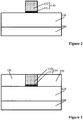
- Figures 1-2 illustrate a corresponding semiconductor structure.
- FIG. 2 is a cross-sectional view along A-A1 direction of the fin portion in Figure 1 .
- a base substrate may be provided.
- the base substrate may include a substrate 100, a fin portion 120 formed on the substrate 100, and a dummy gate structure 130 formed on the fin portion 120 and crossing the fin portion 120.
- the fin portion 120 may include one or more fins.
- the dummy gate structure 130 may cover part of top and side surfaces of the fin portion 120.
- the substrate 100 may provide a platform for subsequent fabrication processes to form the semiconductor device.
- the substrate 100 may include monocrystalline silicon, polysilicon, or amorphous silicon.
- the substrate 100 may also include silicon (Si), germanium (Ge), germanium-silicon alloy (GeSi), silicon carbide (SiC), or gallium arsenide (GaAs) and other Group III-V compounds thereof.
- the substrate 100 may be a silicon substrate.
- Forming the fin portion 120 may include: forming a patterned mask layer on the substrate 100, where the patterned mask layer may define the position of the fin portion 120; and using the patterned mask layer as a mask to etch the substrate 100 and to remove portions of the substrate 100 to form the fin portion 120. Because the fin portion 120 may be formed by etching the substrate 100, the fin portion 120 and the substrate 100 may be made of the same material. In certain embodiments, the fin portion 120 may be made of different material from the substrate 100.
- An isolation structure 110 may also be formed on the substrate 100.
- the surface of the isolation structure 110 may be lower than the top surface of the fin portion 120.
- the isolation structure 110 may be configured to electrically isolate the adjacent fins 120.
- the isolation structure 110 may be made of silicon oxide, or silicon oxynitride, etc.
- the dummy gate structure 130 may include a gate dielectric layer 131 crossing the fin portion 120 and a dummy gate electrode 132 covering the gate dielectric layer 131.
- the gate dielectric layer 131 may be formed on the isolation structure 110, and cover part of top and side surfaces of the fin portion 120.
- the gate dielectric layer 131 may be made of silicon oxide, and the dummy gate electrode 132 may be made of polysilicon.
- a source region, a drain region and an interlayer dielectric layer may be formed (S102).
- Figure 3 illustrates a corresponding semiconductor structure.
- a source region (not labeled) and a drain region (not labeled) may be formed.
- the source region may be formed in the fin portion 120 at one side of the dummy gate structure 130, and the drain region may be formed in the fin portion 120 at other side of the dummy gate structure 130.
- an interlayer dielectric layer 150 may be formed on the base substrate, as shown in Figure 3 .
- the interlayer dielectric layer 150 may cover the sidewall of the dummy gate structure 130, and the top surface of the interlayer dielectric layer 150 may be levelled with the top surface of the dummy gate structure 130.
- the interlayer dielectric layer 150 may be made of silicon oxide, silicon oxynitride, or silicon oxycarbide, etc.
- Forming the interlayer dielectric layer 150 may include forming an interlayer dielectric material layer covering the fin portion 120, the dummy gate structure 130, the isolation structure 110, and the substrate 100. The entire top surface of the interlayer dielectric material layer may be higher than the top surface of the dummy gate structure 130. Forming the interlayer dielectric layer 150 may also include planarizing the interlayer dielectric material layer until the top surface of the dummy gate structure 130 is exposed to form the interlayer dielectric layer 150.
- the top surface of the dummy gate electrode 132 may be easily oxidized in the process environment, resulting in the formation of a silicon oxide layer on the top surface of the dummy gate electrode 132.
- the difference in the conductivity of the silicon oxide layer and the conductivity of the interlayer dielectric layer 150 may be relatively small. If an atomic layer deposition process is directly performed on the surface of the interlayer dielectric layer 150 to form a sacrificial layer, correspondingly, the sacrificial layer may also be formed on the top surface of the dummy gate electrode 132.
- the selectivity of forming the sacrificial layer on the top surface of the interlayer dielectric layer 150 and the top surface of the dummy gate electrode 132 may be small.
- a sacrificial layer may be formed (S103).
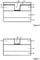
- Figure 4 illustrates a corresponding semiconductor structure.
- a sacrificial layer 160 covering the top surface of the interlayer dielectric layer 150 may be formed by using a selective atomic layer deposition process.
- the sacrificial layer 160 may be made of tantalum nitride, or cobalt nitride, etc.
- the selective atomic layer deposition process may include multiple atomic layer deposition cycles to achieve the desired thickness of the sacrificial layer 160 to be formed on the interlayer dielectric layer 150. To simplify the description, only one atomic layer deposition cycle is described herein.
- the atomic layer deposition cycle may include performing a hydrogen radical treatment on the interlayer dielectric layer 150 and the dummy gate electrode 132. After the hydrogen radical treatment, the atomic layer deposition cycle may also include introducing a precursor into the reaction chamber to be reacted to form the sacrificial layer 160 on the interlayer dielectric layer 150. The sacrificial layer 160 may expose the top surface of the dummy gate electrode 132. Further, the atomic layer deposition cycle may include removing the by-products after the reaction.
- the hydrogen radical may be adsorbed on the top surface of the dummy gate electrode 132. Because of the strong oxidation resistance of the hydrogen radical, the top surface of the dummy gate electrode 132 may not be easily oxidized in the process environment, it is difficult to form the non-conductive silicon oxide layer on the top surface of the dummy gate electrode 132. Therefore, the top surface of the dummy gate electrode 132 and the top surface of the interlayer dielectric layer 150 may exhibit different electrical conductivities, and the formed sacrificial layer 160 may be selectively deposited. Specifically, suitable precursor material may be used. The precursor may be easily adsorbed on the top surface of the interlayer dielectric layer 150 and reacted to form the sacrificial layer 160.
- the sacrificial layer 160 may not be formed on the top surface of the dummy gate electrode 132 when forming the sacrificial layer 160 on the top surface of the interlayer dielectric layer 150. Therefore, the sacrificial layer 160 with a desired thickness can be selectively formed on the top surface of the interlayer dielectric layer 150, instead of being formed on the top surface of the dummy gate electrode 132.
- the parameters of the hydrogen radical treatment may include the following.
- the gas used may include methane, or hydrogen, etc; and the process temperature may be in a range of approximately 50 °C - 400 °C. If the time of the hydrogen radical treatment is too short, the top surface of the interlayer dielectric layer 150 and the top surface of the dummy gate electrode 132 may exhibit small difference in electrical conductivity after the hydrogen radical treatment. The selectivity of forming the sacrificial layer 160 on the top surface of the interlayer dielectric layer 150 may decrease. If the time of the hydrogen radical treatment is too long, the process cost may be increased. Therefore, in one embodiment, the time of the hydrogen radical treatment may be in a range of approximately 5 seconds - 40 seconds.
- the process of forming the sacrificial layer 160 on the interlayer dielectric layer 150 by introducing the precursor into the reaction chamber to be reacted may include: proving the precursor including a first precursor and a second precursor; first introducing the first precursor into the reaction chamber, where the first precursor may be adsorbed on the interlayer dielectric layer 150; removing the excess first precursor in the chamber; then introducing the second precursor into the reaction chamber, where the second precursor may be reacted with the first precursor to form the sacrificial layer 160; and removing the by-products including the remaining second precursor, the product formed by reaction of the second precursor and the first precursor after the reaction.
- the reaction parameters of the precursor may include the following.
- the first precursor used may be NH 3
- the second precursor used may be Ta(NMe 2 ) 5 (pentyl (Methylamino) tantalum, PDMAT)
- the temperature may be in a range of approximately 100 °C - 300 °C
- the chamber pressure may be in a range of approximately 1 Torr - 10 Torr.
- the reaction parameters of the precursor may include the following.
- the first precursor used may be C 7 H 5 CoO 2 (dicarbonyl cyclopentadienyl cobalt)
- the second precursor used may be NH 3
- the temperature may be in a range of approximately 100 °C - 300 °C
- the chamber pressure may be in a range of approximately 1 Torr - 10 Torr.
- the thickness of the sacrificial layer 160 should be in a suitable range. If the thickness of the sacrificial layer is less than 20 ⁇ , the protective effect of the sacrificial layer 160 on the interlayer dielectric layer 150 may be reduced, causing a portion of the sacrificial layer 160 to be etched through, and that the interlayer dielectric layer 150 under the sacrificial layer 160 are damaged by the etching when subsequently removing the dummy gate electrode 132. In this case, the height of a portion of the interlayer dielectric layer 150 may be changed, causing the height of the subsequently formed metal gate electrode to be ineffectively controlled. If the thickness of the sacrificial layer 160 is larger than 100 ⁇ , the process cost may be increased. Therefore, the thickness of the sacrificial layer 160 may be in a range of approximately 20 ⁇ -100 ⁇ .
- a sidewall spacer may be formed on the sidewall of the dummy gate structure 130.
- the interlayer dielectric layer 150 may also cover the sidewall of the sidewall spacer, and the formed sacrificial layer 160 may also cover the top surface of the sidewall spacer.
- the hydrogen radical treatment may also be performed on the top surface of the sidewall spacer.
- FIG. 5 illustrates a corresponding semiconductor structure.
- an opening 170 may be formed by using the sacrificial layer 160 as a mask to remove the dummy gate electrode 132 (shown in Figure 4 ).
- the dummy gate electrode 132 may be removed by using a dry etching process, or a wet etching process, etc.
- a metal gate electrode may be formed (S105).
- Figure 6 illustrates a corresponding semiconductor structure.
- a metal gate electrode 180 may be formed on the sacrificial layer 160 and in the opening 170.
- the metal gate electrode 180 may be made of a metal, including one of more of W, Al, Ti, Cu, Mo, and Pt.
- the process of forming the metal gate electrode 180 may be a deposition process, or an electroplating process, etc.
- the entire surface of the metal gate electrode 180 may be higher than the surface of the sacrificial layer 160.
- the metal gate electrode and the sacrificial layer may be planarized (S106).
- Figure 7 illustrates a corresponding semiconductor structure.
- the metal gate electrode 180 and the sacrificial layer 160 may be planarized until the top surface of the metal gate electrode 180 is levelled with the top surface of the interlayer dielectric layer 150.
- the process of planarizing the metal gate electrode 180 and the sacrificial layer 160 may be a chemical mechanical polishing process.
- a barrier layer (not labeled) covering the gate dielectric layer 131 and a working function layer (not labeled) covering the barrier layer may be formed.
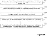
- FIG. 23 illustrates another exemplary fabrication process to form a semiconductor device consistent with the disclosed embodiments; and Figures 8-12 illustrate semiconductor structures corresponding to certain stages of the exemplary fabrication process.
- a base substrate with certain structures maybe formed (S201).
- Figure 8 illustrates a corresponding semiconductor structure.
- a base substrate may be provided.
- the base substrate may include a substrate 200, a dummy gate structure 210 and an interlayer dielectric layer 230 covering the sidewall of the dummy gate structure 210 and formed on the substrate 200.
- the top surface of the interlayer dielectric layer 230 may be levelled with the top surface of the dummy gate structure 210.
- a source region (not labeled) and a drain region (not labeled) may be formed.
- the source region may be formed in the substrate 200 at one side of the dummy gate structure 210, and the drain region may be formed in the substrate 200 at other side of the dummy gate structure 210.
- the interlayer dielectric layer 230 may be formed.
- the dummy gate structure 210 may include a gate dielectric layer 211 formed on the substrate 200 and a dummy gate electrode 212 formed on the gate dielectric layer 211.
- the gate dielectric layer 211 may be made of silicon oxide, and the dummy gate electrode 212 may be made of polysilicon.
- the method of forming the dummy gate structure 210 and the interlayer dielectric layer 230 can be referred to the above-described embodiment.
- a sacrificial layer may be formed (S202).
- Figure 9 illustrates a corresponding semiconductor structure.
- a sacrificial layer 240 covering the top surface of the interlayer dielectric layer 230 may be formed by using a selective atomic layer deposition process.
- the sacrificial layer 240 may be made of tantalum nitride, or cobalt nitride, etc.
- the thickness of the sacrificial layer 240 may be in a range of approximately 20 ⁇ - 100 ⁇ .
- the selective atomic layer deposition process configured to form the sacrificial layer 240 may include multiple atomic layer deposition cycles to achieve the desired thickness of the sacrificial layer 240 to be formed on the interlayer dielectric layer 230. To simplify the description, only one atomic layer deposition cycle is described herein.
- the atomic layer deposition cycle may include performing a hydrogen radical treatment on the interlayer dielectric layer 230 and the dummy gate electrode 212. After the hydrogen radical treatment, the atomic layer deposition cycle may also include introducing a precursor into the reaction chamber to be reacted to form the sacrificial layer 240 on the interlayer dielectric layer 230.
- the sacrificial layer 240 may expose the top surface of the dummy gate electrode 212. Further, the atomic layer deposition cycle may include removing the by-products after the reaction.
- the parameters of the hydrogen radical treatment can be referred to the above-described embodiment and are not repeated herein.
- the process and parameters of the reaction of the precursor configured to form the sacrificial layer 240 can also be referred to the above-described embodiment and are not repeated herein.
- a sidewall spacer may be formed on the sidewall of the dummy gate structure 210.
- the interlayer dielectric layer 230 may also cover the sidewall of the sidewall spacer, and the formed sacrificial layer 240 may also cover the top surface of the sidewall spacer.
- the hydrogen radical treatment may also be performed on the top surface of the sidewall spacer.
- FIG. 10 illustrates a corresponding semiconductor structure.
- an opening 250 may be formed by using the sacrificial layer 240 as a mask to remove the dummy gate electrode 212 (shown in Figure 9 ).
- the method of removing the dummy gate electrode 212 can be referred to the process of removing the dummy gate electrode 132 in the above-described embodiment and is not repeated herein.
- a metal gate electrode may be formed (S204).
- Figure 11 illustrates a corresponding semiconductor structure.
- a metal gate electrode 260 may be formed on the sacrificial layer 240 and in the opening 250.
- the method of forming the metal gate electrode 260 can be referred to the process of forming the metal gate electrode 180 in the above-described embodiment and is not repeated herein.
- the metal gate electrode and the sacrificial layer may be planarized (S205).
- Figure 12 illustrates a corresponding semiconductor structure.
- the metal gate electrode 260 and the sacrificial layer 240 may be planarized until the top surface of the metal gate electrode 260 is levelled with the top surface of the interlayer dielectric layer 230.
- the process of planarizing the metal gate electrode 260 and the sacrificial layer 240 may be a chemical mechanical polishing process.
- a barrier layer (not labeled) covering the gate dielectric layer 211 and a working function layer (not labeled) covering the barrier layer may be formed.
- the sacrificial layer covering the top surface of the interlayer dielectric layer may be formed by using the selective atomic layer deposition process, the sacrificial layer may only expose the top surface of the dummy gate electrode. Therefore, during the process of removing the dummy gate electrode, the sacrificial layer can protect the top surface of the interlayer dielectric layer from being damaged by the etching, so as to prevent the height of the interlayer dielectric layer from being decreased and changed during the process of removing the dummy gate electrode. After planarizing the metal gate electrode and the sacrificial layer, the top surface of the metal gate electrode may be levelled with the top surface of the interlayer dielectric layer.
- the height of the interlayer dielectric layer may not be changed, the height of the metal gate electrode may not be changed either. Therefore, the height of the finally formed metal gate electrode can be controlled.
- the selective atomic layer deposition process is performed to form the sacrificial layer. Forming the sacrificial layer on the top surface of the interlayer dielectric layer and not forming the sacrificial layer on the top surface of the dummy gate electrode can be achieved in one single process step, simplifying the process of forming the sacrificial layer.
- FIG. 24 illustrates another exemplary fabrication process to form a semiconductor device consistent with the disclosed embodiments; and Figures 13-21 illustrate semiconductor structures corresponding to certain stages of the exemplary fabrication process.
- a base substrate with certain structures may be formed (S301).
- Figure 13 illustrates a corresponding semiconductor structure.
- a base substrate 300 may be provided.
- the base substrate may include a first region (I region) and a second region (II region).
- a first dummy gate structure 310 may be formed on the base substrate 300 in the first region, and a second dummy gate structure 320 may be formed on the base substrate 300 in the second region.
- An interlayer dielectric layer 330 covering the sidewall of the first dummy gate structure 310 and the sidewall of the second dummy gate structure 320 may be formed on the base substrate 300.
- the top surface of the interlayer dielectric layer 330 may be levelled with the top surfaces of the first dummy gate structure 310 and the second dummy gate structure 320.
- the first region may be a P-type region, and the second region may be an N-type region. Or the first region may be an N-type region, and the second region may be a P-type region.
- a P-type MOS transistor may be formed in the P-type region, and an N-type MOS transistor may be formed in the N-type region.
- the first dummy gate structure 310 may include a first gate dielectric layer 311 formed on the base substrate 300 in the first region, and a first dummy gate electrode 312 formed on the first gate dielectric layer 311.
- the second dummy gate structure 320 may include a second gate dielectric layer 321 formed on the base substrate 300 in the second region, and a second dummy gate electrode 322 formed on the second gate dielectric layer 321.
- Forming the first dummy gate structure 310 and the second dummy gate structure 320 may include: sequentially forming a gate dielectric material layer on the base substrate 300 and a dummy gate electrode material layer on the gate dielectric material layer; forming a patterned mask layer on the dummy gate electrode material layer, configured to define the first dummy gate structure 310 and the second dummy gate structure 320; and using the mask layer as a mask to sequentially etch the dummy gate electrode material layer and the gate dielectric material layer to form the first dummy gate structure 310 and the second dummy gate structure 320.
- the first gate dielectric layer 311 and the second gate dielectric layer 321 may be made of silicon oxide.
- the first dummy gate electrode 312 and the second dummy gate electrode 322 may be made of polysilicon.
- first source and drain regions may be formed in the base substrate 300 at both sides of the first dummy gate structure 310.
- Second source and drain regions may be formed in the base substrate 300 at both sides of the second dummy gate structure 320.
- the interlayer dielectric layer 330 may be formed.
- the interlayer dielectric layer 330 may be made of silicon oxide, silicon oxynitride, or silicon oxycarbide, etc. Forming the interlayer dielectric layer 330 may include forming an interlayer dielectric material layer to cover the first dummy gate structure 310 and the second dummy gate structure 320. The entire surface of the interlayer dielectric material layer may be higher than the top surfaces of the first dummy gate structure 310 and the second dummy gate structure 320. Forming the interlayer dielectric layer 330 may also include planarizing the interlayer dielectric material layer until the top surfaces of the first dummy gate structure 310 and the second dummy gate structure 320 are exposed to form the interlayer dielectric layer 330.
- a first sacrificial layer may be formed (S302).
- Figure 14 illustrates a corresponding semiconductor structure.
- a first sacrificial layer 340 may be formed on the top surface of the interlayer dielectric layer 330 by using a selective atomic layer deposition process.
- the first sacrificial layer 340 may be made of tantalum nitride, or cobalt nitride, etc, and the thickness of the first sacrificial layer 340 may be in a range of approximately 20 ⁇ 100 ⁇ .
- the selective atomic layer deposition process configured to form the first sacrificial layer 340 may include multiple atomic layer deposition cycles to achieve the desired thickness of the first sacrificial layer 340 formed on the interlayer dielectric layer 330. To simplify the description, only one atomic layer deposition cycle is described herein.
- the atomic layer deposition cycle may include performing a hydrogen radical treatment on the interlayer dielectric layer 330, the first dummy gate electrode 312 and the second dummy gate electrode 322. After the hydrogen radical treatment, the atomic layer deposition cycle may also include introducing a precursor into the reaction chamber to be reacted to form the first sacrificial layer 340 on the interlayer dielectric layer 330. Further, the atomic layer deposition cycle may include removing the by-products after the reaction.
- the parameters of the hydrogen radical treatment may include as following.
- the gas used may be methane, or hydrogen, etc
- the process temperature may be in a range of approximately 50 °C - 400 °C
- the time may be in a range of approximately 5 seconds - 40 seconds.
- the process of forming the first sacrificial layer 340 on the interlayer dielectric layer 330 by introducing the precursor into the reaction chamber to be reacted may include: providing the precursor including a first precursor and a second precursor; first introducing the first precursor into the reaction chamber, where the first precursor may be adsorbed on the interlayer dielectric layer 330; removing the excess first precursor in the chamber; then introducing the second precursor into the reaction chamber, where the second precursor may be reacted with the first precursor to form the first sacrificial layer 340; and removing the by-products including the remaining second precursor, the product formed by reaction of the second precursor and the first precursor after the reaction.
- the reaction parameters of the precursor may include the following.
- the first precursor used may be NH 3
- the second precursor used may be Ta(NMe 2 ) 5
- the temperature may be in a range of approximately 100 °C - 300 °C
- the chamber pressure may be in a range of approximately 1 Torr - 10 Torr.
- the reaction parameters of the precursor may include as following.
- the first precursor used may be C 7 H 5 CoO 2
- the second precursor used may be NH 3
- the temperature may be in a range of approximately 100 °C - 300 °C
- the chamber pressure may be in a range of approximately 1 Torr - 10 Torr.
- a first opening may be formed (S303).
- Figure 15 illustrates a corresponding semiconductor structure.
- a first opening 313 may be formed by removing the first dummy gate electrode 312.
- the process of removing the first dummy gate electrode 312 may be a dry etching process, or a wet etching process, etc.
- a first metal gate electrode may be formed (S304).
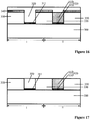
- Figure 16 illustrates a corresponding semiconductor structure.
- a first metal gate electrode 350 may be formed on the first sacrificial layer 340 and in the first opening 313 (shown in Figure 15 ).
- the first metal gate electrode 350 may be made of metal, including one or more of W, Al, Ti, Cu, Mo, and Pt.
- the process of forming the first metal gate electrode 350 may be a deposition process, or an electroplating process, etc.
- the entire surface of the first metal gate electrode 350 may be higher than the top surface of the first sacrificial layer 340.
- the first metal gate electrode and the first sacrificial layer may be planarized (S305).
- Figure 17 illustrates a corresponding semiconductor structure.
- the first metal gate electrode 350 and the first sacrificial layer 340 may be planarized until the top surface of the first metal gate electrode 350 is levelled with the top surface of the interlayer dielectric layer 330.
- the process of planarizing the first metal gate electrode 350 and the first sacrificial layer 340 may be a chemical mechanical polishing process.
- a second sacrificial layer may be formed (S306).
- Figure 18 illustrates a corresponding semiconductor structure.
- a second sacrificial layer 360 covering the surface of the interlayer dielectric layer 330 may be formed by using the selective atomic layer deposition process.
- the process of forming the second sacrificial layer 360 can be referred to the process of forming the first sacrificial layer 340, and is not repeated herein.
- a second opening may be formed (S307).
- Figure 19 illustrates a corresponding semiconductor structure.
- a second opening 323 may be formed by removing the second dummy gate electrode 322.
- the process of removing the second dummy gate electrode 322 may be a dry etching process, or a wet etching process, etc.
- a second metal gate electrode may be formed (S308).
- Figure 20 illustrates a corresponding semiconductor structure.
- a second metal gate electrode 370 may be formed on the second sacrificial layer 360 and in the second opening 323.
- the second metal gate electrode 370 may be made of metal, including one or more of W, Al, Ti, Cu, Mo, and Pt.
- the process of forming the second metal gate electrode 370 may be a deposition process, or an electroplating process, etc.
- the entire surface of the second metal gate electrode 370 may be higher than the top surface of the second sacrificial layer 360.
- the second metal gate electrode and the second sacrificial layer may be planarized (S309).
- Figure 21 illustrates a corresponding semiconductor structure.
- the second metal gate electrode 370 and the second sacrificial layer 360 may be planarized until the top surface of the second metal gate electrode 370 is levelled with the top surface of the interlayer dielectric layer 330.
- the process of planarizing the second metal gate electrode 370 and the second sacrificial layer 360 may be a chemical mechanical polishing process.
- the first sacrificial layer covering the top surface of the interlayer dielectric layer may be formed by using the selective atomic layer deposition process, the first sacrificial layer may expose the top surfaces of the first dummy gate electrode and the second dummy gate electrode. Therefore, during the process of removing the first dummy gate electrode, the first sacrificial layer can protect the top surface of the interlayer dielectric layer from being damaged by the etching, so as to prevent the height of the interlayer dielectric layer from being decreased and changed during the process of removing the first dummy gate electrode. After planarizing the first metal gate electrode and the first sacrificial layer, the top surface of the first metal gate electrode may be levelled with the top surface of the interlayer dielectric layer.
- the height of the interlayer dielectric layer may not be changed, the height of the first metal gate electrode may not be changed either. Because the second sacrificial layer covering the top surface of the interlayer dielectric layer may be formed by using the selective atomic layer deposition process, the second sacrificial layer may expose the top surfaces of the first metal gate electrode and the second dummy gate electrode. Therefore, during the process of removing the second dummy gate electrode, the second sacrificial layer can protect the top surface of the interlayer dielectric layer from being damaged by the etching, so as to prevent the height of the interlayer dielectric layer from being decreased and changed during the process of removing the second dummy gate electrode.
- the top surface of the second metal gate electrode may be levelled with the top surface of the interlayer dielectric layer. Because the height of the interlayer dielectric layer may not be changed, the height of the second metal gate electrode may not be changed either. Therefore, the heights of the finally formed first metal gate electrode and second metal gate electrode can be controlled.
- a first barrier layer covering the first gate dielectric layer and a first working function layer covering the first barrier layer may be formed before forming the first metal gate electrode.
- a second barrier layer covering the second gate dielectric layer and a second working function layer covering the second barrier layer may be formed before forming the first metal gate electrode.
- the selective atomic layer deposition process may be performed to form the sacrificial layer covering the top surface of the interlayer dielectric layer.
- Forming the sacrificial layer on the top surface of the interlayer dielectric layer and not forming the sacrificial layer on the top surface of the dummy gate electrode can be achieved in one single process step, simplifying the process of forming the sacrificial layer.
- the sacrificial layer may be formed, the sacrificial layer can protect the top surface of the interlayer dielectric layer from being damaged by the etching, so as to prevent the height of the interlayer dielectric layer from being decreased and changed during the process of removing the dummy gate electrode.
- the top surface of the metal gate electrode may be levelled with the top surface of the interlayer dielectric layer. Because the height of the interlayer dielectric layer may not be changed, the height of the metal gate electrode may not be changed either. Therefore, the height of the finally formed metal gate electrode can be controlled.
- the hydrogen radical treatment may be performed on the interlayer dielectric layer and the dummy gate electrode when forming the sacrificial layer by using the selective atomic layer deposition process, and it may be difficult to form the non-conductive silicon oxide layer on the top surface of the dummy gate electrode. Therefore, the top surface of the dummy gate electrode and the top surface of the interlayer dielectric layer may exhibit different electrical conductivities, and the precursor may be easily adsorbed on the top surface of the interlayer dielectric layer and be reacted to form the sacrificial layer.
- the sacrificial layer can be selectively formed on the top surface of the interlayer dielectric layer, instead of being formed on the top surface of the dummy gate electrode.
Landscapes
- Electrodes Of Semiconductors (AREA)
- Insulated Gate Type Field-Effect Transistor (AREA)
- Chemical & Material Sciences (AREA)
- Composite Materials (AREA)
- Engineering & Computer Science (AREA)
- Materials Engineering (AREA)
Abstract
Description
- This application claims the priority of Chinese patent application No.
201510881899.7, filed on December 03,2015 - The present invention generally relates to the field of semiconductor manufacturing technology and, more particularly, relates to a semiconductor device and fabrication method thereof.
- Metal-Oxide-Semiconductor (MOS) transistor is one of the most important components in modern integrated circuits. The basic structure of the MOS transistor includes a semiconductor substrate, a gate structure formed on the semiconductor substrate, a source region formed at one side of the gate structure, and a drain region formed at other side of the gate structure. The gate structure includes a gate dielectric layer formed on the semiconductor substrate, and a gate electrode layer formed on the gate dielectric layer. The source region and the drain region are doped with ions.
- With the increasing of integration degree of the MOS transistor, the voltage and current required for operating the MOS transistor continue to reduce, and the switching speed of the transistor accelerates accordingly, thus more requirements of the semiconductor fabrication process are substantially needed. Therefore, high dielectric constant material (high-K material) has been used instead of SiO2 as a gate dielectric layer to better isolate the gate structure and the other parts of the MOS transistor, and to reduce leakage current. At the same time, to be compatible with the high-K (K larger than 3.9) dielectric constant material, metal material has been used instead of the original polysilicon as the gate electrode layer. The high-K gate dielectric layer and the metal gate electrode form a metal gate structure, so as to further reduce the leakage current of the MOS transistor.
- A gate-last process is usually used to form the MOS transistor having the metal gate structure. During the gate-last process, a dummy gate structure is first formed on the semiconductor substrate, and an interlayer dielectric layer is formed on the semiconductor substrate at both sides of the dummy gate structure. The top surface of the interlayer dielectric layer is levelled with the top surface of the dummy gate structure. Then the dummy gate electrode is removed, and the metal gate electrode is formed at a position previously defined by the dummy gate electrode.
- However, the height of the metal gate electrode cannot be controlled by the existing techniques to form the semiconductor device. The disclosed device structures and methods are directed to solve one or more problems set forth above and other problems.
- A first aspect of the present invention includes a method for fabricating a semiconductor device. The method includes providing a base substrate including a first dummy gate electrode and an interlayer dielectric layer covering a sidewall of the first dummy gate electrode. The method also includes forming a first sacrificial layer covering a top surface of the interlayer dielectric layer by using a selective atomic layer deposition process, wherein the first sacrificial layer exposes a top surface of the dummy gate electrode. In addition, the method includes forming a first opening by using the first sacrificial layer as an etch mask to remove the first dummy gate electrode, and forming a first metal gate electrode on the first sacrificial layer and in the opening. Further, the method includes planarizing the first metal gate electrode and the first sacrificial layer until a top surface of the first metal gate electrode is levelled with the top surface of the interlayer dielectric layer.
- A thickness of the first sacrificial layer is preferably in a range of approximately 20 Å - 100 Å and/or the first sacrificial layer is preferably made of tantalum nitride, or cobalt nitride.
- In a further development of the present invention the method includes providing the base substrate including the first dummy gate electrode in a first region, a second dummy gate electrode in a second region, and an interlayer dielectric layer formed on sidewalls of the first dummy gate electrode and the second dummy gate electrode, and having the top surface coplanar with the first dummy gate electrode and the second dummy gate electrode. The method also includes forming the first sacrificial layer on a top surface of the interlayer dielectric layer by using the selective atomic layer deposition process, and forming the first opening by removing the first dummy gate electrode after forming the first sacrificial layer. In addition, the method includes forming the first metal gate electrode on the first sacrificial layer and in the first opening, and planarizing the first metal gate electrode and the first sacrificial layer until a top surface of the first metal gate electrode is levelled with the top surface of the interlayer dielectric layer. Moreover, the method includes forming a second sacrificial layer covering the top surface of the interlayer dielectric layer by using selective atomic layer deposition process after planarizing the first metal gate electrode and the first sacrificial layer, and forming a second opening by removing the second dummy gate electrode after forming the second sacrificial layer. Further, the method includes forming a second metal gate electrode on the second sacrificial layer and in the second opening, and planarizing the second metal gate electrode and the second sacrificial layer until a top surface of the second metal gate electrode is levelled with the top surface of the interlayer dielectric layer.
- A thickness of the second sacrificial layer is preferably in a range of approximately 20 Å - - 100 Å and/or the second sacrificial layer is preferably made of tantalum nitride, or cobalt nitride.
- The top surface of the interlayer dielectric layer is preferably levelled with a top surface of the first dummy gate electrode. If appropriate, i.e. in the further development, the top surface of the interlayer dielectric layer is preferably also levelled with a top surface of the second dummy gate electrode.
- The selective atomic layer deposition process may include: performing a hydrogen radical treatment on the interlayer dielectric layer and the first dummy gate electrode and/or, if appropriate, the second dummy gate electrode; introducing a precursor into a reaction chamber to be reacted to form the first sacrificial layer and/or, if appropriate, the second sacrificial layer on the interlayer dielectric layer after the hydrogen radical treatment; and removing by-products after the reaction.
- Parameters of the hydrogen radical treatment may include: a gas including methane, or hydrogen; a process time in a range of approximately 5 seconds - 40 seconds; and a process temperature in a range of approximately 50 °C - 400 °C.
- When the first sacrificial layer is and/or, if appropriate, the second sacrificial layer is made of tantalum nitride, reaction parameters of the precursor may include: the precursor including NH3 and Ta(NMe2)5; a temperature in a range of approximately 100 °C - 300 °C; and a chamber pressure in a range of approximately 1 Torr - 10 Torr.
- When the first sacrificial layer is and/or, if appropriate, the second sacrificial layer is made of cobalt nitride, reaction parameters of the precursor include: the precursor including C7H5CoO2 and NH3; a temperature in a range of approximately 100 °C - 300 °C; and a chamber pressure in a range of approximately 1 Torr - 10 Torr.
- A process of removing the first dummy gate electrode and/or, if appropriate, the second dummy gate electrode may be a dry etching process, or a wet etching process.
- The first metal gate electrode and/or, if appropriate, the second metal gate electrode may be made of a metal, including one or more of W, Al, Ti, Cu, Mo, and Pt.
- A process of forming the first metal gate electrode and/or, if appropriate, the second metal gate electrode may be a deposition process, or an electroplating process.
- An entire surface of the first metal gate electrode in the first opening may be above the first sacrificial layer and/or, if appropriate, an entire surface of the second metal gate electrode in the second opening may be above the second sacrificial layer.
- The method may further include: forming a source region in the base substrate at one side of the first dummy gate electrode; and forming a drain region in the base substrate at other side of the first dummy gate electrode, and/or, if appropriate, forming a source region in the base substrate at one side of the second dummy gate electrode; and forming a drain region in the base substrate at other side of the second dummy gate electrode.
- The method may further include: before forming the first metal gate electrode, further including: forming a first barrier layer on a first gate dielectric layer; and forming a first working function layer on the first barrier layer; and/or, if appropriate before forming the second metal gate electrode, forming a second barrier layer on a second gate dielectric layer; and forming a second working function layer on the second barrier layer.
- The method may further include: forming a source region in the base substrate at one side of the first dummy gate electrode; and forming a drain region in the base substrate at other side of the first dummy gate electrode.
- If appropriate, the method may further include: forming a source region in the base substrate at one side of the second dummy gate electrode; and forming a drain region in the base substrate at other side of the second dummy gate electrode.
- Before forming the first metal gate electrode and/or, if appropriate, the second metal gate electrode, the method may further include: forming a barrier layer on a gate dielectric layer; and forming a working function layer on the barrier layer.
- A third aspect of the present invention includes a semiconductor device. The semiconductor device includes a substrate, and a metal gate electrode structure on the substrate. The semiconductor device also includes an interlayer dielectric layer on the substrate and covering a sidewall of the metal gate electrode, wherein the metal gate electrode structure is formed by: forming a sacrificial layer covering a top surface of the interlayer dielectric layer by using a selective atomic layer deposition process, wherein the sacrificial layer exposes a top surface of a dummy gate electrode; forming an opening by using the sacrificial layer as an etch mask to remove the dummy gate electrode; forming a metal gate electrode on the sacrificial layer and in the opening; and planarizing the metal gate electrode and the sacrificial layer until a top surface of the metal gate electrode is levelled with the top surface of the interlayer dielectric layer.
- Other aspects of the present invention can be understood by those skilled in the art in light of the description, the claims, and the drawings of the present invention.
-
-
Figures 1-7 illustrate semiconductor structures corresponding to certain stages of an exemplary fabrication process to form a semiconductor device consistent with the disclosed embodiments; -
Figures 8-12 illustrate semiconductor structures corresponding to certain stages of another exemplary fabrication process to form a semiconductor device consistent with the disclosed embodiments; -
Figures 13-21 illustrate semiconductor structures corresponding to certain stages of another exemplary fabrication process to form a semiconductor device consistent with the disclosed embodiments; -
Figure 22 illustrates an exemplary fabrication process to form a semiconductor device consistent with the disclosed embodiments; -
Figure 23 illustrates another exemplary fabrication process to form a semiconductor device consistent with the disclosed embodiments; and -
Figure 24 illustrates another exemplary fabrication process to form a semiconductor device consistent with the disclosed embodiments. - Reference will now be made in detail to exemplary embodiments of the invention, which are illustrated in the accompanying drawings. Wherever possible, the same reference numbers will be used throughout the drawings to refer to the same or the alike parts.
- Forming the semiconductor device by the existing fabrication process may include proving a base substrate. The base substrate may include a dummy gate electrode, and an interlayer dielectric layer covering the sidewall of the dummy gate electrode. The top surface of the interlayer dielectric layer is levelled with the top surface of the dummy gate electrode. Forming the semiconductor device may also include removing the dummy gate electrode to form an opening, and forming a metal gate electrode on the surface of the interlayer dielectric layer and in the opening. Further, forming the semiconductor device may include planarizing the metal gate electrode using the interlayer dielectric layer as a stop layer.
- The process of removing the dummy gate electrode usually includes an etching process, such as a wet etching process, or a dry etching process, etc. Because the interlayer dielectric layer is also exposed to an etching environment when removing the dummy gate electrode, the top surface of the interlayer dielectric layer is damaged by etching, causing the thickness of the interlayer dielectric layer to be decreased and to be changed. The variation of the thickness of the interlayer dielectric layer is uncertain, and the thickness of the interlayer dielectric layer after removing the dummy gate electrode cannot be controlled. After finally forming the metal gate electrode, the top surface of the metal gate electrode is levelled with the top surface of the interlayer dielectric layer. Because the thickness of the interlayer dielectric layer cannot be controlled, the thickness of the metal gate electrode cannot be controlled.
- The present invention provides a semiconductor device and fabrication process thereof. Before removing the dummy gate electrode, a sacrificial layer covering the top surface of the interlayer dielectric layer may be formed by a selective atomic layer deposition process. The sacrificial layer may only expose the top surface of the dummy gate electrode, and the height of the finally formed metal gate electrode can be controlled.
- In one embodiment, a semiconductor device configured to form a FinFET is described herein as an example.
Figure 22 illustrates an exemplary fabrication process to form a semiconductor device consistent with the disclosed embodiments; andFigures 1-7 illustrate semiconductor structures corresponding to certain stages of the exemplary fabrication process. - As shown in
Figure 22 , at the beginning of the fabrication process, a base substrate with certain structures may be provided (S101).Figures 1-2 illustrate a corresponding semiconductor structure. -
Figure 2 is a cross-sectional view along A-A1 direction of the fin portion inFigure 1 . Referring toFigure 1 andFigure 2 , a base substrate may be provided. The base substrate may include asubstrate 100, afin portion 120 formed on thesubstrate 100, and adummy gate structure 130 formed on thefin portion 120 and crossing thefin portion 120. Thefin portion 120 may include one or more fins. Thedummy gate structure 130 may cover part of top and side surfaces of thefin portion 120. - The
substrate 100 may provide a platform for subsequent fabrication processes to form the semiconductor device. Thesubstrate 100 may include monocrystalline silicon, polysilicon, or amorphous silicon. Thesubstrate 100 may also include silicon (Si), germanium (Ge), germanium-silicon alloy (GeSi), silicon carbide (SiC), or gallium arsenide (GaAs) and other Group III-V compounds thereof. In one embodiment, thesubstrate 100 may be a silicon substrate. - Forming the
fin portion 120 may include: forming a patterned mask layer on thesubstrate 100, where the patterned mask layer may define the position of thefin portion 120; and using the patterned mask layer as a mask to etch thesubstrate 100 and to remove portions of thesubstrate 100 to form thefin portion 120. Because thefin portion 120 may be formed by etching thesubstrate 100, thefin portion 120 and thesubstrate 100 may be made of the same material. In certain embodiments, thefin portion 120 may be made of different material from thesubstrate 100. - An
isolation structure 110 may also be formed on thesubstrate 100. The surface of theisolation structure 110 may be lower than the top surface of thefin portion 120. Theisolation structure 110 may be configured to electrically isolate theadjacent fins 120. Theisolation structure 110 may be made of silicon oxide, or silicon oxynitride, etc. - The
dummy gate structure 130 may include agate dielectric layer 131 crossing thefin portion 120 and adummy gate electrode 132 covering thegate dielectric layer 131. Thegate dielectric layer 131 may be formed on theisolation structure 110, and cover part of top and side surfaces of thefin portion 120. In one embodiment, thegate dielectric layer 131 may be made of silicon oxide, and thedummy gate electrode 132 may be made of polysilicon. - Returning to
Figure 22 , after forming the base substrate, a source region, a drain region and an interlayer dielectric layer may be formed (S102).Figure 3 illustrates a corresponding semiconductor structure. - A source region (not labeled) and a drain region (not labeled) may be formed. The source region may be formed in the
fin portion 120 at one side of thedummy gate structure 130, and the drain region may be formed in thefin portion 120 at other side of thedummy gate structure 130. After forming the source region and the drain region, aninterlayer dielectric layer 150 may be formed on the base substrate, as shown inFigure 3 . Theinterlayer dielectric layer 150 may cover the sidewall of thedummy gate structure 130, and the top surface of theinterlayer dielectric layer 150 may be levelled with the top surface of thedummy gate structure 130. Theinterlayer dielectric layer 150 may be made of silicon oxide, silicon oxynitride, or silicon oxycarbide, etc. - Forming the
interlayer dielectric layer 150 may include forming an interlayer dielectric material layer covering thefin portion 120, thedummy gate structure 130, theisolation structure 110, and thesubstrate 100. The entire top surface of the interlayer dielectric material layer may be higher than the top surface of thedummy gate structure 130. Forming theinterlayer dielectric layer 150 may also include planarizing the interlayer dielectric material layer until the top surface of thedummy gate structure 130 is exposed to form theinterlayer dielectric layer 150. - Because the
dummy gate electrode 132 may be made of polysilicon, the top surface of thedummy gate electrode 132 may be easily oxidized in the process environment, resulting in the formation of a silicon oxide layer on the top surface of thedummy gate electrode 132. The difference in the conductivity of the silicon oxide layer and the conductivity of theinterlayer dielectric layer 150 may be relatively small. If an atomic layer deposition process is directly performed on the surface of theinterlayer dielectric layer 150 to form a sacrificial layer, correspondingly, the sacrificial layer may also be formed on the top surface of thedummy gate electrode 132. The selectivity of forming the sacrificial layer on the top surface of theinterlayer dielectric layer 150 and the top surface of thedummy gate electrode 132 may be small. - Returning to
Figure 22 , after forming the interlayer dielectric layer, a sacrificial layer may be formed (S103).Figure 4 illustrates a corresponding semiconductor structure. - Referring to
Figure 4 , asacrificial layer 160 covering the top surface of theinterlayer dielectric layer 150 may be formed by using a selective atomic layer deposition process. Thesacrificial layer 160 may be made of tantalum nitride, or cobalt nitride, etc. - The selective atomic layer deposition process may include multiple atomic layer deposition cycles to achieve the desired thickness of the
sacrificial layer 160 to be formed on theinterlayer dielectric layer 150. To simplify the description, only one atomic layer deposition cycle is described herein. The atomic layer deposition cycle may include performing a hydrogen radical treatment on theinterlayer dielectric layer 150 and thedummy gate electrode 132. After the hydrogen radical treatment, the atomic layer deposition cycle may also include introducing a precursor into the reaction chamber to be reacted to form thesacrificial layer 160 on theinterlayer dielectric layer 150. Thesacrificial layer 160 may expose the top surface of thedummy gate electrode 132. Further, the atomic layer deposition cycle may include removing the by-products after the reaction. - Because the hydrogen radical treatment is used, the hydrogen radical may be adsorbed on the top surface of the
dummy gate electrode 132. Because of the strong oxidation resistance of the hydrogen radical, the top surface of thedummy gate electrode 132 may not be easily oxidized in the process environment, it is difficult to form the non-conductive silicon oxide layer on the top surface of thedummy gate electrode 132. Therefore, the top surface of thedummy gate electrode 132 and the top surface of theinterlayer dielectric layer 150 may exhibit different electrical conductivities, and the formedsacrificial layer 160 may be selectively deposited. Specifically, suitable precursor material may be used. The precursor may be easily adsorbed on the top surface of theinterlayer dielectric layer 150 and reacted to form thesacrificial layer 160. During each selective atomic layer deposition reaction, by controlling the thickness of the formedsacrificial layer 160, thesacrificial layer 160 may not be formed on the top surface of thedummy gate electrode 132 when forming thesacrificial layer 160 on the top surface of theinterlayer dielectric layer 150. Therefore, thesacrificial layer 160 with a desired thickness can be selectively formed on the top surface of theinterlayer dielectric layer 150, instead of being formed on the top surface of thedummy gate electrode 132. - The parameters of the hydrogen radical treatment may include the following. The gas used may include methane, or hydrogen, etc; and the process temperature may be in a range of approximately 50 °C - 400 °C. If the time of the hydrogen radical treatment is too short, the top surface of the
interlayer dielectric layer 150 and the top surface of thedummy gate electrode 132 may exhibit small difference in electrical conductivity after the hydrogen radical treatment. The selectivity of forming thesacrificial layer 160 on the top surface of theinterlayer dielectric layer 150 may decrease. If the time of the hydrogen radical treatment is too long, the process cost may be increased. Therefore, in one embodiment, the time of the hydrogen radical treatment may be in a range of approximately 5 seconds - 40 seconds. - The process of forming the
sacrificial layer 160 on theinterlayer dielectric layer 150 by introducing the precursor into the reaction chamber to be reacted may include: proving the precursor including a first precursor and a second precursor; first introducing the first precursor into the reaction chamber, where the first precursor may be adsorbed on theinterlayer dielectric layer 150; removing the excess first precursor in the chamber; then introducing the second precursor into the reaction chamber, where the second precursor may be reacted with the first precursor to form thesacrificial layer 160; and removing the by-products including the remaining second precursor, the product formed by reaction of the second precursor and the first precursor after the reaction. - When the
sacrificial layer 160 is made of tantalum nitride, the reaction parameters of the precursor may include the following. The first precursor used may be NH3, the second precursor used may be Ta(NMe2)5 (pentyl (Methylamino) tantalum, PDMAT), the temperature may be in a range of approximately 100 °C - 300 °C, and the chamber pressure may be in a range of approximately 1 Torr - 10 Torr. - When the
sacrificial layer 160 is made of cobalt nitride, the reaction parameters of the precursor may include the following. The first precursor used may be C7H5CoO2 (dicarbonyl cyclopentadienyl cobalt), the second precursor used may be NH3, the temperature may be in a range of approximately 100 °C - 300 °C, and the chamber pressure may be in a range of approximately 1 Torr - 10 Torr. - The thickness of the
sacrificial layer 160 should be in a suitable range. If the thickness of the sacrificial layer is less than 20 Å, the protective effect of thesacrificial layer 160 on theinterlayer dielectric layer 150 may be reduced, causing a portion of thesacrificial layer 160 to be etched through, and that theinterlayer dielectric layer 150 under thesacrificial layer 160 are damaged by the etching when subsequently removing thedummy gate electrode 132. In this case, the height of a portion of theinterlayer dielectric layer 150 may be changed, causing the height of the subsequently formed metal gate electrode to be ineffectively controlled. If the thickness of thesacrificial layer 160 is larger than 100 Å, the process cost may be increased. Therefore, the thickness of thesacrificial layer 160 may be in a range of approximately 20 Å -100 Å. - In certain embodiments, a sidewall spacer may be formed on the sidewall of the
dummy gate structure 130. Theinterlayer dielectric layer 150 may also cover the sidewall of the sidewall spacer, and the formedsacrificial layer 160 may also cover the top surface of the sidewall spacer. During the hydrogen radical treatment of forming thesacrificial layer 160, the hydrogen radical treatment may also be performed on the top surface of the sidewall spacer. - Returning to
Figure 22 , after forming the sacrificial layer, an opening may be formed (S104).Figure 5 illustrates a corresponding semiconductor structure. - Referring to
Figure 5 , anopening 170 may be formed by using thesacrificial layer 160 as a mask to remove the dummy gate electrode 132 (shown inFigure 4 ). Thedummy gate electrode 132 may be removed by using a dry etching process, or a wet etching process, etc. - Returning to
Figure 22 , after forming the opening, a metal gate electrode may be formed (S105).Figure 6 illustrates a corresponding semiconductor structure. - Referring to
Figure 6 , ametal gate electrode 180 may be formed on thesacrificial layer 160 and in theopening 170. Themetal gate electrode 180 may be made of a metal, including one of more of W, Al, Ti, Cu, Mo, and Pt. The process of forming themetal gate electrode 180 may be a deposition process, or an electroplating process, etc. The entire surface of themetal gate electrode 180 may be higher than the surface of thesacrificial layer 160. - Returning to
Figure 22 , after forming the metal gate electrode, the metal gate electrode and the sacrificial layer may be planarized (S106).Figure 7 illustrates a corresponding semiconductor structure. - Referring to
Figure 7 , themetal gate electrode 180 and thesacrificial layer 160 may be planarized until the top surface of themetal gate electrode 180 is levelled with the top surface of theinterlayer dielectric layer 150. The process of planarizing themetal gate electrode 180 and thesacrificial layer 160 may be a chemical mechanical polishing process. - In one embodiment, before forming the
metal gate electrode 180, optionally, a barrier layer (not labeled) covering thegate dielectric layer 131 and a working function layer (not labeled) covering the barrier layer may be formed. - In another embodiment, a semiconductor device configured to form a planar MOS transistor is described herein as an example.
Figure 23 illustrates another exemplary fabrication process to form a semiconductor device consistent with the disclosed embodiments; andFigures 8-12 illustrate semiconductor structures corresponding to certain stages of the exemplary fabrication process. - As shown in
Figure 23 , at the beginning of the fabrication process, a base substrate with certain structures maybe formed (S201).Figure 8 illustrates a corresponding semiconductor structure. - Referring to
Figure 8 , a base substrate may be provided. The base substrate may include asubstrate 200, adummy gate structure 210 and aninterlayer dielectric layer 230 covering the sidewall of thedummy gate structure 210 and formed on thesubstrate 200. The top surface of theinterlayer dielectric layer 230 may be levelled with the top surface of thedummy gate structure 210. - In one embodiment, after forming the
dummy gate structure 210, a source region (not labeled) and a drain region (not labeled) may be formed. The source region may be formed in thesubstrate 200 at one side of thedummy gate structure 210, and the drain region may be formed in thesubstrate 200 at other side of thedummy gate structure 210. Then, theinterlayer dielectric layer 230 may be formed. - The
dummy gate structure 210 may include agate dielectric layer 211 formed on thesubstrate 200 and a dummy gate electrode 212 formed on thegate dielectric layer 211. Thegate dielectric layer 211 may be made of silicon oxide, and the dummy gate electrode 212 may be made of polysilicon. The method of forming thedummy gate structure 210 and theinterlayer dielectric layer 230 can be referred to the above-described embodiment. - Returning to
Figure 23 , after providing the base substrate, a sacrificial layer may be formed (S202).Figure 9 illustrates a corresponding semiconductor structure. - Referring to
Figure 9 , asacrificial layer 240 covering the top surface of theinterlayer dielectric layer 230 may be formed by using a selective atomic layer deposition process. Thesacrificial layer 240 may be made of tantalum nitride, or cobalt nitride, etc. The thickness of thesacrificial layer 240 may be in a range of approximately 20 Å - 100 Å. - The selective atomic layer deposition process configured to form the
sacrificial layer 240 may include multiple atomic layer deposition cycles to achieve the desired thickness of thesacrificial layer 240 to be formed on theinterlayer dielectric layer 230. To simplify the description, only one atomic layer deposition cycle is described herein. The atomic layer deposition cycle may include performing a hydrogen radical treatment on theinterlayer dielectric layer 230 and the dummy gate electrode 212. After the hydrogen radical treatment, the atomic layer deposition cycle may also include introducing a precursor into the reaction chamber to be reacted to form thesacrificial layer 240 on theinterlayer dielectric layer 230. Thesacrificial layer 240 may expose the top surface of the dummy gate electrode 212. Further, the atomic layer deposition cycle may include removing the by-products after the reaction. - The parameters of the hydrogen radical treatment can be referred to the above-described embodiment and are not repeated herein. The process and parameters of the reaction of the precursor configured to form the
sacrificial layer 240 can also be referred to the above-described embodiment and are not repeated herein. - In certain embodiments, a sidewall spacer may be formed on the sidewall of the
dummy gate structure 210. Theinterlayer dielectric layer 230 may also cover the sidewall of the sidewall spacer, and the formedsacrificial layer 240 may also cover the top surface of the sidewall spacer. During the hydrogen radical treatment of forming thesacrificial layer 240, the hydrogen radical treatment may also be performed on the top surface of the sidewall spacer. - Returning to
Figure 23 , after forming the sacrificial layer, an opening may be formed (S203).Figure 10 illustrates a corresponding semiconductor structure. - Referring to
Figure 10 , an opening 250 may be formed by using thesacrificial layer 240 as a mask to remove the dummy gate electrode 212 (shown inFigure 9 ). The method of removing the dummy gate electrode 212 can be referred to the process of removing thedummy gate electrode 132 in the above-described embodiment and is not repeated herein. - Returning to
Figure 23 , after forming the opening, a metal gate electrode may be formed (S204).Figure 11 illustrates a corresponding semiconductor structure. - Referring to
Figure 11 , ametal gate electrode 260 may be formed on thesacrificial layer 240 and in the opening 250. The method of forming themetal gate electrode 260 can be referred to the process of forming themetal gate electrode 180 in the above-described embodiment and is not repeated herein. - Returning to
Figure 23 , after forming the metal gate electrode, the metal gate electrode and the sacrificial layer may be planarized (S205).Figure 12 illustrates a corresponding semiconductor structure. - Referring to
Figure 12 , themetal gate electrode 260 and thesacrificial layer 240 may be planarized until the top surface of themetal gate electrode 260 is levelled with the top surface of theinterlayer dielectric layer 230. The process of planarizing themetal gate electrode 260 and thesacrificial layer 240 may be a chemical mechanical polishing process. - In one embodiment, before forming the
metal gate electrode 260, optionally, a barrier layer (not labeled) covering thegate dielectric layer 211 and a working function layer (not labeled) covering the barrier layer may be formed. - In the above-described embodiments described in
Figures 1-7 andFigures 8-12 , because the sacrificial layer covering the top surface of the interlayer dielectric layer may be formed by using the selective atomic layer deposition process, the sacrificial layer may only expose the top surface of the dummy gate electrode. Therefore, during the process of removing the dummy gate electrode, the sacrificial layer can protect the top surface of the interlayer dielectric layer from being damaged by the etching, so as to prevent the height of the interlayer dielectric layer from being decreased and changed during the process of removing the dummy gate electrode. After planarizing the metal gate electrode and the sacrificial layer, the top surface of the metal gate electrode may be levelled with the top surface of the interlayer dielectric layer. Because the height of the interlayer dielectric layer may not be changed, the height of the metal gate electrode may not be changed either. Therefore, the height of the finally formed metal gate electrode can be controlled. In addition, the selective atomic layer deposition process is performed to form the sacrificial layer. Forming the sacrificial layer on the top surface of the interlayer dielectric layer and not forming the sacrificial layer on the top surface of the dummy gate electrode can be achieved in one single process step, simplifying the process of forming the sacrificial layer. - In another embodiment, a semiconductor device configured to form two planar MOS transistors is described herein as an example.
Figure 24 illustrates another exemplary fabrication process to form a semiconductor device consistent with the disclosed embodiments; andFigures 13-21 illustrate semiconductor structures corresponding to certain stages of the exemplary fabrication process. - As shown in
Figure 24 , at the beginning of the fabrication process, a base substrate with certain structures may be formed (S301).Figure 13 illustrates a corresponding semiconductor structure. - Referring to
Figure 13 , abase substrate 300 may be provided. The base substrate may include a first region (I region) and a second region (II region). A firstdummy gate structure 310 may be formed on thebase substrate 300 in the first region, and a seconddummy gate structure 320 may be formed on thebase substrate 300 in the second region. Aninterlayer dielectric layer 330 covering the sidewall of the firstdummy gate structure 310 and the sidewall of the seconddummy gate structure 320 may be formed on thebase substrate 300. The top surface of theinterlayer dielectric layer 330 may be levelled with the top surfaces of the firstdummy gate structure 310 and the seconddummy gate structure 320. - The first region may be a P-type region, and the second region may be an N-type region. Or the first region may be an N-type region, and the second region may be a P-type region. A P-type MOS transistor may be formed in the P-type region, and an N-type MOS transistor may be formed in the N-type region.
- The first
dummy gate structure 310 may include a firstgate dielectric layer 311 formed on thebase substrate 300 in the first region, and a firstdummy gate electrode 312 formed on the firstgate dielectric layer 311. The seconddummy gate structure 320 may include a secondgate dielectric layer 321 formed on thebase substrate 300 in the second region, and a seconddummy gate electrode 322 formed on the secondgate dielectric layer 321. - Forming the first
dummy gate structure 310 and the seconddummy gate structure 320 may include: sequentially forming a gate dielectric material layer on thebase substrate 300 and a dummy gate electrode material layer on the gate dielectric material layer; forming a patterned mask layer on the dummy gate electrode material layer, configured to define the firstdummy gate structure 310 and the seconddummy gate structure 320; and using the mask layer as a mask to sequentially etch the dummy gate electrode material layer and the gate dielectric material layer to form the firstdummy gate structure 310 and the seconddummy gate structure 320. In one embodiment, the firstgate dielectric layer 311 and the secondgate dielectric layer 321 may be made of silicon oxide. The firstdummy gate electrode 312 and the seconddummy gate electrode 322 may be made of polysilicon. - After forming the first
dummy gate structure 310 and the seconddummy gate structure 320, first source and drain regions may be formed in thebase substrate 300 at both sides of the firstdummy gate structure 310. Second source and drain regions may be formed in thebase substrate 300 at both sides of the seconddummy gate structure 320. Then, theinterlayer dielectric layer 330 may be formed. - The
interlayer dielectric layer 330 may be made of silicon oxide, silicon oxynitride, or silicon oxycarbide, etc. Forming theinterlayer dielectric layer 330 may include forming an interlayer dielectric material layer to cover the firstdummy gate structure 310 and the seconddummy gate structure 320. The entire surface of the interlayer dielectric material layer may be higher than the top surfaces of the firstdummy gate structure 310 and the seconddummy gate structure 320. Forming theinterlayer dielectric layer 330 may also include planarizing the interlayer dielectric material layer until the top surfaces of the firstdummy gate structure 310 and the seconddummy gate structure 320 are exposed to form theinterlayer dielectric layer 330. - Returning to
Figure 24 , after providing the base substrate, a first sacrificial layer may be formed (S302).Figure 14 illustrates a corresponding semiconductor structure. - Referring to
Figure 14 , a firstsacrificial layer 340 may be formed on the top surface of theinterlayer dielectric layer 330 by using a selective atomic layer deposition process. The firstsacrificial layer 340 may be made of tantalum nitride, or cobalt nitride, etc, and the thickness of the firstsacrificial layer 340 may be in a range of approximately 20 Å 100 Å. - The selective atomic layer deposition process configured to form the first
sacrificial layer 340 may include multiple atomic layer deposition cycles to achieve the desired thickness of the firstsacrificial layer 340 formed on theinterlayer dielectric layer 330. To simplify the description, only one atomic layer deposition cycle is described herein. The atomic layer deposition cycle may include performing a hydrogen radical treatment on theinterlayer dielectric layer 330, the firstdummy gate electrode 312 and the seconddummy gate electrode 322. After the hydrogen radical treatment, the atomic layer deposition cycle may also include introducing a precursor into the reaction chamber to be reacted to form the firstsacrificial layer 340 on theinterlayer dielectric layer 330. Further, the atomic layer deposition cycle may include removing the by-products after the reaction. - The parameters of the hydrogen radical treatment may include as following. The gas used may be methane, or hydrogen, etc, the process temperature may be in a range of approximately 50 °C - 400 °C, and the time may be in a range of approximately 5 seconds - 40 seconds.
- The process of forming the first
sacrificial layer 340 on theinterlayer dielectric layer 330 by introducing the precursor into the reaction chamber to be reacted may include: providing the precursor including a first precursor and a second precursor; first introducing the first precursor into the reaction chamber, where the first precursor may be adsorbed on theinterlayer dielectric layer 330; removing the excess first precursor in the chamber; then introducing the second precursor into the reaction chamber, where the second precursor may be reacted with the first precursor to form the firstsacrificial layer 340; and removing the by-products including the remaining second precursor, the product formed by reaction of the second precursor and the first precursor after the reaction. - When the first
sacrificial layer 340 is made of tantalum nitride, the reaction parameters of the precursor may include the following. The first precursor used may be NH3, the second precursor used may be Ta(NMe2)5, the temperature may be in a range of approximately 100 °C - 300 °C, and the chamber pressure may be in a range of approximately 1 Torr - 10 Torr. - When the first
sacrificial layer 340 is made of cobalt nitride, the reaction parameters of the precursor may include as following. The first precursor used may be C7H5CoO2, the second precursor used may be NH3, the temperature may be in a range of approximately 100 °C - 300 °C, and the chamber pressure may be in a range of approximately 1 Torr - 10 Torr. - Returning to
Figure 24 , after forming the first sacrificial layer, a first opening may be formed (S303).Figure 15 illustrates a corresponding semiconductor structure. - Referring to
Figure 15 , after forming the firstsacrificial layer 340, afirst opening 313 may be formed by removing the firstdummy gate electrode 312. The process of removing the firstdummy gate electrode 312 may be a dry etching process, or a wet etching process, etc. - Returning to
Figure 24 , after forming the first opening, a first metal gate electrode may be formed (S304).Figure 16 illustrates a corresponding semiconductor structure. - Referring to
Figure 16 , a firstmetal gate electrode 350 may be formed on the firstsacrificial layer 340 and in the first opening 313 (shown inFigure 15 ). The firstmetal gate electrode 350 may be made of metal, including one or more of W, Al, Ti, Cu, Mo, and Pt. The process of forming the firstmetal gate electrode 350 may be a deposition process, or an electroplating process, etc. The entire surface of the firstmetal gate electrode 350 may be higher than the top surface of the firstsacrificial layer 340. - Returning to
Figure 24 , after forming the first metal gate electrode, the first metal gate electrode and the first sacrificial layer may be planarized (S305).Figure 17 illustrates a corresponding semiconductor structure. - Referring to
Figure 17 , the firstmetal gate electrode 350 and the firstsacrificial layer 340 may be planarized until the top surface of the firstmetal gate electrode 350 is levelled with the top surface of theinterlayer dielectric layer 330. The process of planarizing the firstmetal gate electrode 350 and the firstsacrificial layer 340 may be a chemical mechanical polishing process. - Returning to
Figure 24 , after planarizing the first metal gate electrode and the first sacrificial layer, a second sacrificial layer may be formed (S306).Figure 18 illustrates a corresponding semiconductor structure. - Referring to
Figure 18 , after planarizing the firstmetal gate electrode 350 and the firstsacrificial layer 340, a secondsacrificial layer 360 covering the surface of theinterlayer dielectric layer 330 may be formed by using the selective atomic layer deposition process. The process of forming the secondsacrificial layer 360 can be referred to the process of forming the firstsacrificial layer 340, and is not repeated herein. - Returning to
Figure 24 , after forming the second sacrificial layer, a second opening may be formed (S307).Figure 19 illustrates a corresponding semiconductor structure. - Referring to
Figure 19 , after forming the secondsacrificial layer 360, asecond opening 323 may be formed by removing the seconddummy gate electrode 322. The process of removing the seconddummy gate electrode 322 may be a dry etching process, or a wet etching process, etc. - Returning to
Figure 24 , after forming the second opening, a second metal gate electrode may be formed (S308).Figure 20 illustrates a corresponding semiconductor structure. - Referring to
Figure 20 , a secondmetal gate electrode 370 may be formed on the secondsacrificial layer 360 and in thesecond opening 323. The secondmetal gate electrode 370 may be made of metal, including one or more of W, Al, Ti, Cu, Mo, and Pt. The process of forming the secondmetal gate electrode 370 may be a deposition process, or an electroplating process, etc. The entire surface of the secondmetal gate electrode 370 may be higher than the top surface of the secondsacrificial layer 360. - Returning to
Figure 24 , after forming the second metal gate electrode, the second metal gate electrode and the second sacrificial layer may be planarized (S309).Figure 21 illustrates a corresponding semiconductor structure. - Referring to
Figure 21 , the secondmetal gate electrode 370 and the secondsacrificial layer 360 may be planarized until the top surface of the secondmetal gate electrode 370 is levelled with the top surface of theinterlayer dielectric layer 330. The process of planarizing the secondmetal gate electrode 370 and the secondsacrificial layer 360 may be a chemical mechanical polishing process. - In one embodiment, because the first sacrificial layer covering the top surface of the interlayer dielectric layer may be formed by using the selective atomic layer deposition process, the first sacrificial layer may expose the top surfaces of the first dummy gate electrode and the second dummy gate electrode. Therefore, during the process of removing the first dummy gate electrode, the first sacrificial layer can protect the top surface of the interlayer dielectric layer from being damaged by the etching, so as to prevent the height of the interlayer dielectric layer from being decreased and changed during the process of removing the first dummy gate electrode. After planarizing the first metal gate electrode and the first sacrificial layer, the top surface of the first metal gate electrode may be levelled with the top surface of the interlayer dielectric layer. Because the height of the interlayer dielectric layer may not be changed, the height of the first metal gate electrode may not be changed either. Because the second sacrificial layer covering the top surface of the interlayer dielectric layer may be formed by using the selective atomic layer deposition process, the second sacrificial layer may expose the top surfaces of the first metal gate electrode and the second dummy gate electrode. Therefore, during the process of removing the second dummy gate electrode, the second sacrificial layer can protect the top surface of the interlayer dielectric layer from being damaged by the etching, so as to prevent the height of the interlayer dielectric layer from being decreased and changed during the process of removing the second dummy gate electrode. After planarizing the second metal gate electrode and the second sacrificial layer, the top surface of the second metal gate electrode may be levelled with the top surface of the interlayer dielectric layer. Because the height of the interlayer dielectric layer may not be changed, the height of the second metal gate electrode may not be changed either. Therefore, the heights of the finally formed first metal gate electrode and second metal gate electrode can be controlled.
- In one embodiment, before forming the first metal gate electrode, optionally, a first barrier layer covering the first gate dielectric layer and a first working function layer covering the first barrier layer may be formed. Before forming the second metal gate electrode, optionally, a second barrier layer covering the second gate dielectric layer and a second working function layer covering the second barrier layer may be formed.
- Accordingly, the selective atomic layer deposition process may be performed to form the sacrificial layer covering the top surface of the interlayer dielectric layer. Forming the sacrificial layer on the top surface of the interlayer dielectric layer and not forming the sacrificial layer on the top surface of the dummy gate electrode can be achieved in one single process step, simplifying the process of forming the sacrificial layer. In addition, because the sacrificial layer may be formed, the sacrificial layer can protect the top surface of the interlayer dielectric layer from being damaged by the etching, so as to prevent the height of the interlayer dielectric layer from being decreased and changed during the process of removing the dummy gate electrode. After planarizing the metal gate electrode and the sacrificial layer, the top surface of the metal gate electrode may be levelled with the top surface of the interlayer dielectric layer. Because the height of the interlayer dielectric layer may not be changed, the height of the metal gate electrode may not be changed either. Therefore, the height of the finally formed metal gate electrode can be controlled.
- Further, the hydrogen radical treatment may be performed on the interlayer dielectric layer and the dummy gate electrode when forming the sacrificial layer by using the selective atomic layer deposition process, and it may be difficult to form the non-conductive silicon oxide layer on the top surface of the dummy gate electrode. Therefore, the top surface of the dummy gate electrode and the top surface of the interlayer dielectric layer may exhibit different electrical conductivities, and the precursor may be easily adsorbed on the top surface of the interlayer dielectric layer and be reacted to form the sacrificial layer. During each selective atomic layer deposition reaction, by controlling the thickness of the formed sacrificial layer, forming the sacrificial layer on the top surface of the dummy gate electrode and not forming the sacrificial layer on the top surface of the interlayer dielectric layer can be achieved. Therefore, the sacrificial layer can be selectively formed on the top surface of the interlayer dielectric layer, instead of being formed on the top surface of the dummy gate electrode.
Claims (15)
- A method for fabricating a semiconductor device, comprising:providing a base substrate including a first dummy gate electrode and an interlayer dielectric layer covering a sidewall of the first dummy gate electrode;forming a first sacrificial layer covering a top surface of the interlayer dielectric layer by using a selective atomic layer deposition process, wherein the sacrificial layer exposes a top surface of the first dummy gate electrode, wherein preferably a thickness of the first sacrificial layer is in a range of approximately 20 Å - 100 Å and/or the first sacrificial layer is made of tantalum nitride, or cobalt nitride;forming a first opening by using the first sacrificial layer as an etch mask to remove the first dummy gate electrode;forming a first metal gate electrode on the first sacrificial layer and in the first opening; andplanarizing the first metal gate electrode and the first sacrificial layer until a top surface of the first metal gate electrode is levelled with the top surface of the interlayer dielectric layer.
- The method according to claim 1, further comprising:providing the base substrate including the first dummy gate electrode in a first region, a second dummy gate electrode in a second region, and the interlayer dielectric layer formed on sidewalls of the first dummy gate electrode and the second dummy gate electrode, and having a top surface coplanar with the first dummy gate electrode and the second dummy gate electrode;forming the first sacrificial layer on a top surface of the interlayer dielectric layer by using the selective atomic layer deposition process;forming the first opening by removing the first dummy gate electrode after forming the first sacrificial layer;forming the first metal gate electrode on the first sacrificial layer and in the first opening;planarizing the first metal gate electrode and the first sacrificial layer until a top surface of the first metal gate electrode is levelled with the top surface of the interlayer dielectric layer;forming a second sacrificial layer covering the top surface of the interlayer dielectric layer by using the selective atomic layer deposition process after planarizing the first metal gate electrode and the first sacrificial layer, wherein preferably a thickness of the second sacrificial layer is in a range of approximately 20 Å - 100 Å and/or the second sacrificial layer is made of tantalum nitride, or cobalt nitride;forming a second opening by removing the second dummy gate electrode after forming the second sacrificial layer;forming a second metal gate electrode on the second sacrificial layer and in the second opening; andplanarizing the second metal gate electrode and the second sacrificial layer until a top surface of the second metal gate electrode is levelled with the top surface of the interlayer dielectric layer.
- The method according to claim 1 or 2, wherein:the top surface of the interlayer dielectric layer is levelled with a top surface of the first dummy gate electrode and/or, if appropriate, the second dummy gate electrode.
- The method according to any one of the claims 1-3, wherein the selective atomic layer deposition process includes:performing a hydrogen radical treatment on the interlayer dielectric layer and the first dummy gate electrode and/or, if appropriate, the second dummy gate electrode;introducing a precursor into a reaction chamber to be reacted to form the first sacrificial layer and/or, if appropriate, the second sacrificial layer on the interlayer dielectric layer after the hydrogen radical treatment; andremoving by-products after the reaction.
- The method according to claim 4, wherein parameters of the hydrogen radical treatment include:a gas including methane, or hydrogen;a process time in a range of approximately 5 seconds - 40 seconds; anda process temperature in a range of approximately 50 °C - 400 °C.
- The method according to claim 4 or 5, wherein, when the first sacrificial layer and, if appropriate, the second sacrificial layer is made of tantalum nitride, reaction parameters of the precursor include:the precursor including NH3 and Ta(NMe2)5;a temperature in a range of approximately 100 °C - 300 °C; anda chamber pressure in a range of approximately 1 Torr - 10 Torr.
- The method according to claim 4 or 5, wherein, when the first sacrificial layer and, if appropriate, the second sacrificial layer is made of cobalt nitride, reaction parameters of the precursor include:the precursor including C7H5CoO2 and NH3;a temperature in a range of approximately 100 °C - 300 °C; anda chamber pressure in a range of approximately 1 Torr - 10 Torr.
- The method according to any one of the claims 1-7, wherein:a process of removing the first dummy gate electrode and, if appropriate, the second dummy gate electrode is a dry etching process, or a wet etching process.
- The method according to any one of the claims 1-8, wherein:the first metal gate electrode and, if appropriate, the second metal gate electrode is made of a metal, including one or more of W, Al, Ti, Cu, Mo, and Pt.
- The method according to any one of the claims 1-9, wherein:a process of forming the first metal gate electrode and, if appropriate, the second metal gate electrode is a deposition process, or an electroplating process.
- The method according to any one of the claims 1-10, wherein:an entire surface of the first metal gate electrode in the first opening is above the first sacrificial layer, and, if appropriate, an entire surface of the second metal gate electrode in the second opening is above the second sacrificial layer.
- The method according to any one of the claims 1-11, further including:forming a source region in the base substrate at one side of the first dummy gate electrode; and forming a drain region in the base substrate at other side of the first dummy gate electrode; and/or, if appropriate,forming a source region in the base substrate at one side of the second dummy gate electrode; and forming a drain region in the base substrate at other side of the second dummy gate electrode.
- The method according to claims 1-12, further including:before forming the first metal gate electrode, forming a first barrier layer on a first gate dielectric layer; and forming a first working function layer on the first barrier layer; and/or, if appropriatebefore forming the second metal gate electrode, forming a second barrier layer on a second gate dielectric layer; and forming a second working function layer on the second barrier layer.
- A semiconductor device, comprising:a substrate;a metal gate electrode structure on the substrate; andan interlayer dielectric layer on the substrate and covering a sidewall of the metal gate electrode, wherein the metal gate electrode structure is formed by:forming a sacrificial layer covering a top surface of the interlayer dielectric layer by using a selective atomic layer deposition process, wherein the sacrificial layer exposes a top surface of a dummy gate electrode; forming an opening by using the sacrificial layer as an etch mask to remove the dummy gate electrode; forming a metal gate electrode on the sacrificial layer and in the opening; and planarizing the metal gate electrode and the sacrificial layer until a top surface of the metal gate electrode is levelled with the top surface of the interlayer dielectric layer.
- The semiconductor device according to claim 14, further including:a barrier layer on a gate dielectric layer; anda working function layer on the barrier layer.
Applications Claiming Priority (1)
| Application Number | Priority Date | Filing Date | Title |
|---|---|---|---|
| CN201510881899.7A CN106847694B (en) | 2015-12-03 | 2015-12-03 | Method of forming a semiconductor device |
Publications (1)
| Publication Number | Publication Date |
|---|---|
| EP3176828A1 true EP3176828A1 (en) | 2017-06-07 |
Family
ID=57354205
Family Applications (1)
| Application Number | Title | Priority Date | Filing Date |
|---|---|---|---|
| EP16199537.8A Withdrawn EP3176828A1 (en) | 2015-12-03 | 2016-11-18 | Semiconductor device and fabrication method thereof |
Country Status (3)
| Country | Link |
|---|---|
| US (1) | US10297454B2 (en) |
| EP (1) | EP3176828A1 (en) |
| CN (1) | CN106847694B (en) |
Families Citing this family (6)
| Publication number | Priority date | Publication date | Assignee | Title |
|---|---|---|---|---|
| DE102018101016B4 (en) * | 2017-09-29 | 2021-07-29 | Taiwan Semiconductor Manufacturing Co., Ltd. | Process for cutting metal gates and structures formed from them |
| US10490458B2 (en) | 2017-09-29 | 2019-11-26 | Taiwan Semiconductor Manufacturing Company, Ltd. | Methods of cutting metal gates and structures formed thereof |
| CN110729183B (en) * | 2018-07-16 | 2022-08-23 | 中芯国际集成电路制造(上海)有限公司 | Metal gate forming method and semiconductor device |
| CN111696864B (en) * | 2019-03-12 | 2023-12-22 | 中芯国际集成电路制造(上海)有限公司 | Semiconductor devices and methods of forming the same |
| CN112582336B (en) * | 2019-09-29 | 2025-06-27 | 中芯国际集成电路制造(上海)有限公司 | Method for forming a semiconductor device |
| CN114496791B (en) * | 2020-11-11 | 2025-10-31 | 中芯国际集成电路制造(上海)有限公司 | Method for forming semiconductor structure |
Citations (9)
| Publication number | Priority date | Publication date | Assignee | Title |
|---|---|---|---|---|
| US6534412B1 (en) * | 2000-10-11 | 2003-03-18 | United Microelectronics Corp. | Method for removing native oxide |
| US20030219953A1 (en) * | 2002-05-23 | 2003-11-27 | Nec Electronics Corporation | Method for fabricating semiconductor devices |
| US20080132050A1 (en) * | 2006-12-05 | 2008-06-05 | Lavoie Adrien R | Deposition process for graded cobalt barrier layers |
| US20100087056A1 (en) * | 2008-10-06 | 2010-04-08 | Taiwan Semiconductor Manufacturing Company, Ltd. | Method for gate height control in a gate last process |
| US20120264281A1 (en) * | 2011-04-12 | 2012-10-18 | Taiwan Semiconductor Manufacturing Company, Ltd. | Method of fabricating a plurality of gate structures |
| US20130243956A1 (en) * | 2012-03-14 | 2013-09-19 | Applied Materials, Inc. | Selective Atomic Layer Depositions |
| US8546209B1 (en) * | 2012-06-15 | 2013-10-01 | International Business Machines Corporation | Replacement metal gate processing with reduced interlevel dielectric layer etch rate |
| US20150145054A1 (en) * | 2013-11-27 | 2015-05-28 | Semiconductor Manufacturing International (Shanghai) Corporation | Transistor and method for forming the same |
| US20150206956A1 (en) * | 2014-01-21 | 2015-07-23 | Samsung Electronics Co., Ltd. | Semiconductor device and method of manufacturing the same |
Family Cites Families (5)
| Publication number | Priority date | Publication date | Assignee | Title |
|---|---|---|---|---|
| US7929649B2 (en) * | 2004-06-30 | 2011-04-19 | Stmicroelectronics, Inc. | Analog/digital carrier differentiation in digital cable receivers |
| US8058119B2 (en) | 2008-08-27 | 2011-11-15 | Taiwan Semiconductor Manufacturing Company, Ltd. | Device scheme of HKMG gate-last process |
| US8637390B2 (en) * | 2010-06-04 | 2014-01-28 | Applied Materials, Inc. | Metal gate structures and methods for forming thereof |
| US9659814B2 (en) * | 2013-02-01 | 2017-05-23 | Applied Materials, Inc. | Doping control of metal nitride films |
| JP2014236192A (en) * | 2013-06-05 | 2014-12-15 | 東京エレクトロン株式会社 | Formation method of manganese oxide film |
-
2015
- 2015-12-03 CN CN201510881899.7A patent/CN106847694B/en active Active
-
2016
- 2016-10-27 US US15/335,777 patent/US10297454B2/en active Active
- 2016-11-18 EP EP16199537.8A patent/EP3176828A1/en not_active Withdrawn
Patent Citations (9)
| Publication number | Priority date | Publication date | Assignee | Title |
|---|---|---|---|---|
| US6534412B1 (en) * | 2000-10-11 | 2003-03-18 | United Microelectronics Corp. | Method for removing native oxide |
| US20030219953A1 (en) * | 2002-05-23 | 2003-11-27 | Nec Electronics Corporation | Method for fabricating semiconductor devices |
| US20080132050A1 (en) * | 2006-12-05 | 2008-06-05 | Lavoie Adrien R | Deposition process for graded cobalt barrier layers |
| US20100087056A1 (en) * | 2008-10-06 | 2010-04-08 | Taiwan Semiconductor Manufacturing Company, Ltd. | Method for gate height control in a gate last process |
| US20120264281A1 (en) * | 2011-04-12 | 2012-10-18 | Taiwan Semiconductor Manufacturing Company, Ltd. | Method of fabricating a plurality of gate structures |
| US20130243956A1 (en) * | 2012-03-14 | 2013-09-19 | Applied Materials, Inc. | Selective Atomic Layer Depositions |
| US8546209B1 (en) * | 2012-06-15 | 2013-10-01 | International Business Machines Corporation | Replacement metal gate processing with reduced interlevel dielectric layer etch rate |
| US20150145054A1 (en) * | 2013-11-27 | 2015-05-28 | Semiconductor Manufacturing International (Shanghai) Corporation | Transistor and method for forming the same |
| US20150206956A1 (en) * | 2014-01-21 | 2015-07-23 | Samsung Electronics Co., Ltd. | Semiconductor device and method of manufacturing the same |
Also Published As
| Publication number | Publication date |
|---|---|
| CN106847694A (en) | 2017-06-13 |
| US10297454B2 (en) | 2019-05-21 |
| US20170162394A1 (en) | 2017-06-08 |
| CN106847694B (en) | 2019-09-27 |
Similar Documents
| Publication | Publication Date | Title |
|---|---|---|
| KR102073395B1 (en) | A method of manufacturing a semiconductor device with separated merged source/drain structure | |
| US9947766B2 (en) | Semiconductor device and fabricating method thereof | |
| CN106206308B (en) | Method of fabricating a FINFET device | |
| CN103311185B (en) | Method of hybrid high-k/metal-gate stack fabrication | |
| US10297511B2 (en) | Fin-FET device and fabrication method thereof | |
| US9685439B1 (en) | Semiconductor device and manufacturing method thereof | |
| US10615078B2 (en) | Method to recess cobalt for gate metal application | |
| CN112750775A (en) | Method for forming semiconductor device | |
| US10297454B2 (en) | Semiconductor device and fabrication method thereof | |
| CN104835780A (en) | Semiconductor structure and method for manufacturing same | |
| TW201903858A (en) | Methods for fabricating semiconductor devices | |
| US20210375683A1 (en) | Multi-channel devices and methods of manufacture | |
| WO2014029150A1 (en) | Semiconductor structure and manufacturing method therefor | |
| US12557371B2 (en) | Semiconductor structure and method for manufacturing the same | |
| TW202119479A (en) | Semiconductor device structures and methods for formng the same | |
| TW201703156A (en) | Semiconductor device and method of manufacturing same | |
| TWI801923B (en) | Semiconductor device and method of manufacture | |
| CN105990229B (en) | Semiconductor devices and their manufacturing processes | |
| US12446294B2 (en) | Method of manufacturing semiconductor devices having different gate dielectric thickness within one transistor | |
| CN115527944A (en) | Method for manufacturing semiconductor element | |
| CN107591331B (en) | Semiconductor structure and forming method thereof | |
| US20260047196A1 (en) | Semiconductor device and manufacturing method thereof | |
| CN113745113B (en) | Semiconductor devices and methods of forming the same | |
| US20250338599A1 (en) | Semiconductor gate structure and methods of forming the same | |
| TW202547301A (en) | Transistor devices and methods of manufacturing |
Legal Events
| Date | Code | Title | Description |
|---|---|---|---|
| AK | Designated contracting states |
Kind code of ref document: A1 Designated state(s): AL AT BE BG CH CY CZ DE DK EE ES FI FR GB GR HR HU IE IS IT LI LT LU LV MC MK MT NL NO PL PT RO RS SE SI SK SM TR |
|
| AX | Request for extension of the european patent |
Extension state: BA ME |
|
| PUAI | Public reference made under article 153(3) epc to a published international application that has entered the european phase |
Free format text: ORIGINAL CODE: 0009012 |
|
| STAA | Information on the status of an ep patent application or granted ep patent |
Free format text: STATUS: THE APPLICATION HAS BEEN PUBLISHED |
|
| STAA | Information on the status of an ep patent application or granted ep patent |
Free format text: STATUS: REQUEST FOR EXAMINATION WAS MADE |
|
| RAP1 | Party data changed (applicant data changed or rights of an application transferred) |
Owner name: SEMICONDUCTOR MANUFACTURING INTERNATIONAL CORPORAT |
|
| 17P | Request for examination filed |
Effective date: 20170718 |
|
| RBV | Designated contracting states (corrected) |
Designated state(s): AL AT BE BG CH CY CZ DE DK EE ES FI FR GB GR HR HU IE IS IT LI LT LU LV MC MK MT NL NO PL PT RO RS SE SI SK SM TR |
|
| RAP1 | Party data changed (applicant data changed or rights of an application transferred) |
Owner name: SEMICONDUCTOR MANUFACTURING INTERNATIONAL (BEIJING Owner name: SEMICONDUCTOR MANUFACTURING INTERNATIONAL (SHANGHA |
|
| STAA | Information on the status of an ep patent application or granted ep patent |
Free format text: STATUS: EXAMINATION IS IN PROGRESS |
|
| 17Q | First examination report despatched |
Effective date: 20200702 |
|
| STAA | Information on the status of an ep patent application or granted ep patent |
Free format text: STATUS: THE APPLICATION HAS BEEN WITHDRAWN |
|
| 18W | Application withdrawn |
Effective date: 20201006 |