EP3176819A2 - Wafer-level chip-scale package with redistribution layer - Google Patents
Wafer-level chip-scale package with redistribution layer Download PDFInfo
- Publication number
- EP3176819A2 EP3176819A2 EP16199908.1A EP16199908A EP3176819A2 EP 3176819 A2 EP3176819 A2 EP 3176819A2 EP 16199908 A EP16199908 A EP 16199908A EP 3176819 A2 EP3176819 A2 EP 3176819A2
- Authority
- EP
- European Patent Office
- Prior art keywords
- layer
- bonding pad
- passivation layer
- formed over
- portions
- Prior art date
- Legal status (The legal status is an assumption and is not a legal conclusion. Google has not performed a legal analysis and makes no representation as to the accuracy of the status listed.)
- Withdrawn
Links
Images




Classifications
-
- H—ELECTRICITY
- H10—SEMICONDUCTOR DEVICES; ELECTRIC SOLID-STATE DEVICES NOT OTHERWISE PROVIDED FOR
- H10W—GENERIC PACKAGES, INTERCONNECTIONS, CONNECTORS OR OTHER CONSTRUCTIONAL DETAILS OF DEVICES COVERED BY CLASS H10
- H10W74/00—Encapsulations, e.g. protective coatings
- H10W74/10—Encapsulations, e.g. protective coatings characterised by their shape or disposition
- H10W74/131—Encapsulations, e.g. protective coatings characterised by their shape or disposition the semiconductor body being only partially enclosed
- H10W74/147—Encapsulations, e.g. protective coatings characterised by their shape or disposition the semiconductor body being only partially enclosed the encapsulations being multilayered
-
- H—ELECTRICITY
- H10—SEMICONDUCTOR DEVICES; ELECTRIC SOLID-STATE DEVICES NOT OTHERWISE PROVIDED FOR
- H10W—GENERIC PACKAGES, INTERCONNECTIONS, CONNECTORS OR OTHER CONSTRUCTIONAL DETAILS OF DEVICES COVERED BY CLASS H10
- H10W20/00—Interconnections in chips, wafers or substrates
- H10W20/40—Interconnections external to wafers or substrates, e.g. back-end-of-line [BEOL] metallisations or vias connecting to gate electrodes
-
- H—ELECTRICITY
- H10—SEMICONDUCTOR DEVICES; ELECTRIC SOLID-STATE DEVICES NOT OTHERWISE PROVIDED FOR
- H10W—GENERIC PACKAGES, INTERCONNECTIONS, CONNECTORS OR OTHER CONSTRUCTIONAL DETAILS OF DEVICES COVERED BY CLASS H10
- H10W72/00—Interconnections or connectors in packages
- H10W72/20—Bump connectors, e.g. solder bumps or copper pillars; Dummy bumps; Thermal bumps
-
- H—ELECTRICITY
- H10—SEMICONDUCTOR DEVICES; ELECTRIC SOLID-STATE DEVICES NOT OTHERWISE PROVIDED FOR
- H10W—GENERIC PACKAGES, INTERCONNECTIONS, CONNECTORS OR OTHER CONSTRUCTIONAL DETAILS OF DEVICES COVERED BY CLASS H10
- H10W99/00—Subject matter not provided for in other groups of this subclass
-
- H—ELECTRICITY
- H10—SEMICONDUCTOR DEVICES; ELECTRIC SOLID-STATE DEVICES NOT OTHERWISE PROVIDED FOR
- H10W—GENERIC PACKAGES, INTERCONNECTIONS, CONNECTORS OR OTHER CONSTRUCTIONAL DETAILS OF DEVICES COVERED BY CLASS H10
- H10W70/00—Package substrates; Interposers; Redistribution layers [RDL]
- H10W70/60—Insulating or insulated package substrates; Interposers; Redistribution layers
- H10W70/62—Insulating or insulated package substrates; Interposers; Redistribution layers characterised by their interconnections
- H10W70/65—Shapes or dispositions of interconnections
-
- H—ELECTRICITY
- H10—SEMICONDUCTOR DEVICES; ELECTRIC SOLID-STATE DEVICES NOT OTHERWISE PROVIDED FOR
- H10W—GENERIC PACKAGES, INTERCONNECTIONS, CONNECTORS OR OTHER CONSTRUCTIONAL DETAILS OF DEVICES COVERED BY CLASS H10
- H10W70/00—Package substrates; Interposers; Redistribution layers [RDL]
- H10W70/60—Insulating or insulated package substrates; Interposers; Redistribution layers
- H10W70/62—Insulating or insulated package substrates; Interposers; Redistribution layers characterised by their interconnections
- H10W70/65—Shapes or dispositions of interconnections
- H10W70/652—Cross-sectional shapes
-
- H—ELECTRICITY
- H10—SEMICONDUCTOR DEVICES; ELECTRIC SOLID-STATE DEVICES NOT OTHERWISE PROVIDED FOR
- H10W—GENERIC PACKAGES, INTERCONNECTIONS, CONNECTORS OR OTHER CONSTRUCTIONAL DETAILS OF DEVICES COVERED BY CLASS H10
- H10W70/00—Package substrates; Interposers; Redistribution layers [RDL]
- H10W70/60—Insulating or insulated package substrates; Interposers; Redistribution layers
- H10W70/67—Insulating or insulated package substrates; Interposers; Redistribution layers characterised by their insulating layers or insulating parts
- H10W70/68—Shapes or dispositions thereof
-
- H—ELECTRICITY
- H10—SEMICONDUCTOR DEVICES; ELECTRIC SOLID-STATE DEVICES NOT OTHERWISE PROVIDED FOR
- H10W—GENERIC PACKAGES, INTERCONNECTIONS, CONNECTORS OR OTHER CONSTRUCTIONAL DETAILS OF DEVICES COVERED BY CLASS H10
- H10W72/00—Interconnections or connectors in packages
- H10W72/01—Manufacture or treatment
- H10W72/012—Manufacture or treatment of bump connectors, dummy bumps or thermal bumps
-
- H—ELECTRICITY
- H10—SEMICONDUCTOR DEVICES; ELECTRIC SOLID-STATE DEVICES NOT OTHERWISE PROVIDED FOR
- H10W—GENERIC PACKAGES, INTERCONNECTIONS, CONNECTORS OR OTHER CONSTRUCTIONAL DETAILS OF DEVICES COVERED BY CLASS H10
- H10W72/00—Interconnections or connectors in packages
- H10W72/01—Manufacture or treatment
- H10W72/019—Manufacture or treatment of bond pads
- H10W72/01931—Manufacture or treatment of bond pads using blanket deposition
- H10W72/01933—Manufacture or treatment of bond pads using blanket deposition in liquid form, e.g. spin coating, spray coating or immersion coating
- H10W72/01935—Manufacture or treatment of bond pads using blanket deposition in liquid form, e.g. spin coating, spray coating or immersion coating by plating, e.g. electroless plating or electroplating
-
- H—ELECTRICITY
- H10—SEMICONDUCTOR DEVICES; ELECTRIC SOLID-STATE DEVICES NOT OTHERWISE PROVIDED FOR
- H10W—GENERIC PACKAGES, INTERCONNECTIONS, CONNECTORS OR OTHER CONSTRUCTIONAL DETAILS OF DEVICES COVERED BY CLASS H10
- H10W72/00—Interconnections or connectors in packages
- H10W72/01—Manufacture or treatment
- H10W72/019—Manufacture or treatment of bond pads
- H10W72/01931—Manufacture or treatment of bond pads using blanket deposition
- H10W72/01938—Manufacture or treatment of bond pads using blanket deposition in gaseous form, e.g. by CVD or PVD
-
- H—ELECTRICITY
- H10—SEMICONDUCTOR DEVICES; ELECTRIC SOLID-STATE DEVICES NOT OTHERWISE PROVIDED FOR
- H10W—GENERIC PACKAGES, INTERCONNECTIONS, CONNECTORS OR OTHER CONSTRUCTIONAL DETAILS OF DEVICES COVERED BY CLASS H10
- H10W72/00—Interconnections or connectors in packages
- H10W72/01—Manufacture or treatment
- H10W72/0198—Manufacture or treatment batch processes
-
- H—ELECTRICITY
- H10—SEMICONDUCTOR DEVICES; ELECTRIC SOLID-STATE DEVICES NOT OTHERWISE PROVIDED FOR
- H10W—GENERIC PACKAGES, INTERCONNECTIONS, CONNECTORS OR OTHER CONSTRUCTIONAL DETAILS OF DEVICES COVERED BY CLASS H10
- H10W72/00—Interconnections or connectors in packages
- H10W72/20—Bump connectors, e.g. solder bumps or copper pillars; Dummy bumps; Thermal bumps
- H10W72/241—Dispositions, e.g. layouts
-
- H—ELECTRICITY
- H10—SEMICONDUCTOR DEVICES; ELECTRIC SOLID-STATE DEVICES NOT OTHERWISE PROVIDED FOR
- H10W—GENERIC PACKAGES, INTERCONNECTIONS, CONNECTORS OR OTHER CONSTRUCTIONAL DETAILS OF DEVICES COVERED BY CLASS H10
- H10W72/00—Interconnections or connectors in packages
- H10W72/20—Bump connectors, e.g. solder bumps or copper pillars; Dummy bumps; Thermal bumps
- H10W72/241—Dispositions, e.g. layouts
- H10W72/244—Dispositions, e.g. layouts relative to underlying supporting features, e.g. bond pads, RDLs or vias
-
- H—ELECTRICITY
- H10—SEMICONDUCTOR DEVICES; ELECTRIC SOLID-STATE DEVICES NOT OTHERWISE PROVIDED FOR
- H10W—GENERIC PACKAGES, INTERCONNECTIONS, CONNECTORS OR OTHER CONSTRUCTIONAL DETAILS OF DEVICES COVERED BY CLASS H10
- H10W72/00—Interconnections or connectors in packages
- H10W72/20—Bump connectors, e.g. solder bumps or copper pillars; Dummy bumps; Thermal bumps
- H10W72/251—Materials
- H10W72/252—Materials comprising solid metals or solid metalloids, e.g. PbSn, Ag or Cu
-
- H—ELECTRICITY
- H10—SEMICONDUCTOR DEVICES; ELECTRIC SOLID-STATE DEVICES NOT OTHERWISE PROVIDED FOR
- H10W—GENERIC PACKAGES, INTERCONNECTIONS, CONNECTORS OR OTHER CONSTRUCTIONAL DETAILS OF DEVICES COVERED BY CLASS H10
- H10W72/00—Interconnections or connectors in packages
- H10W72/20—Bump connectors, e.g. solder bumps or copper pillars; Dummy bumps; Thermal bumps
- H10W72/29—Bond pads specially adapted therefor
-
- H—ELECTRICITY
- H10—SEMICONDUCTOR DEVICES; ELECTRIC SOLID-STATE DEVICES NOT OTHERWISE PROVIDED FOR
- H10W—GENERIC PACKAGES, INTERCONNECTIONS, CONNECTORS OR OTHER CONSTRUCTIONAL DETAILS OF DEVICES COVERED BY CLASS H10
- H10W72/00—Interconnections or connectors in packages
- H10W72/90—Bond pads, in general
- H10W72/921—Structures or relative sizes of bond pads
- H10W72/922—Bond pads being integral with underlying chip-level interconnections
- H10W72/9223—Bond pads being integral with underlying chip-level interconnections with redistribution layers [RDL]
-
- H—ELECTRICITY
- H10—SEMICONDUCTOR DEVICES; ELECTRIC SOLID-STATE DEVICES NOT OTHERWISE PROVIDED FOR
- H10W—GENERIC PACKAGES, INTERCONNECTIONS, CONNECTORS OR OTHER CONSTRUCTIONAL DETAILS OF DEVICES COVERED BY CLASS H10
- H10W72/00—Interconnections or connectors in packages
- H10W72/90—Bond pads, in general
- H10W72/921—Structures or relative sizes of bond pads
- H10W72/923—Bond pads having multiple stacked layers
-
- H—ELECTRICITY
- H10—SEMICONDUCTOR DEVICES; ELECTRIC SOLID-STATE DEVICES NOT OTHERWISE PROVIDED FOR
- H10W—GENERIC PACKAGES, INTERCONNECTIONS, CONNECTORS OR OTHER CONSTRUCTIONAL DETAILS OF DEVICES COVERED BY CLASS H10
- H10W72/00—Interconnections or connectors in packages
- H10W72/90—Bond pads, in general
- H10W72/921—Structures or relative sizes of bond pads
- H10W72/923—Bond pads having multiple stacked layers
- H10W72/9232—Bond pads having multiple stacked layers with additional elements interposed between layers
-
- H—ELECTRICITY
- H10—SEMICONDUCTOR DEVICES; ELECTRIC SOLID-STATE DEVICES NOT OTHERWISE PROVIDED FOR
- H10W—GENERIC PACKAGES, INTERCONNECTIONS, CONNECTORS OR OTHER CONSTRUCTIONAL DETAILS OF DEVICES COVERED BY CLASS H10
- H10W72/00—Interconnections or connectors in packages
- H10W72/90—Bond pads, in general
- H10W72/941—Dispositions of bond pads
- H10W72/9415—Dispositions of bond pads relative to the surface, e.g. recessed, protruding
-
- H—ELECTRICITY
- H10—SEMICONDUCTOR DEVICES; ELECTRIC SOLID-STATE DEVICES NOT OTHERWISE PROVIDED FOR
- H10W—GENERIC PACKAGES, INTERCONNECTIONS, CONNECTORS OR OTHER CONSTRUCTIONAL DETAILS OF DEVICES COVERED BY CLASS H10
- H10W72/00—Interconnections or connectors in packages
- H10W72/90—Bond pads, in general
- H10W72/941—Dispositions of bond pads
- H10W72/942—Dispositions of bond pads relative to underlying supporting features, e.g. bond pads, RDLs or vias
-
- H—ELECTRICITY
- H10—SEMICONDUCTOR DEVICES; ELECTRIC SOLID-STATE DEVICES NOT OTHERWISE PROVIDED FOR
- H10W—GENERIC PACKAGES, INTERCONNECTIONS, CONNECTORS OR OTHER CONSTRUCTIONAL DETAILS OF DEVICES COVERED BY CLASS H10
- H10W72/00—Interconnections or connectors in packages
- H10W72/90—Bond pads, in general
- H10W72/981—Auxiliary members, e.g. spacers
-
- H—ELECTRICITY
- H10—SEMICONDUCTOR DEVICES; ELECTRIC SOLID-STATE DEVICES NOT OTHERWISE PROVIDED FOR
- H10W—GENERIC PACKAGES, INTERCONNECTIONS, CONNECTORS OR OTHER CONSTRUCTIONAL DETAILS OF DEVICES COVERED BY CLASS H10
- H10W72/00—Interconnections or connectors in packages
- H10W72/90—Bond pads, in general
- H10W72/981—Auxiliary members, e.g. spacers
- H10W72/983—Reinforcing structures, e.g. collars
-
- H—ELECTRICITY
- H10—SEMICONDUCTOR DEVICES; ELECTRIC SOLID-STATE DEVICES NOT OTHERWISE PROVIDED FOR
- H10W—GENERIC PACKAGES, INTERCONNECTIONS, CONNECTORS OR OTHER CONSTRUCTIONAL DETAILS OF DEVICES COVERED BY CLASS H10
- H10W74/00—Encapsulations, e.g. protective coatings
- H10W74/10—Encapsulations, e.g. protective coatings characterised by their shape or disposition
- H10W74/111—Encapsulations, e.g. protective coatings characterised by their shape or disposition the semiconductor body being completely enclosed
- H10W74/129—Encapsulations, e.g. protective coatings characterised by their shape or disposition the semiconductor body being completely enclosed forming a chip-scale package [CSP]
Definitions
- the present invention relates to integrated circuits (ICs), and in particular to a wafer-level chip scale package (WLCSP) with a redistribution layer and a method of manufacturing the same.
- ICs integrated circuits
- WLCSP wafer-level chip scale package
- the desire to make electronic products small, lightweight, and high-performing has developed into a desire to make electronic parts small, lightweight, and high-performing.
- This desire has caused developments to proceed in various packaging technologies, along with developments in the technologies related to designing and manufacturing semiconductors.
- Representative examples of packaging technologies include the ball grid array (BGA), the flip-chip, and the chip scale package (CSP) based on area array and surface-mount packaging.
- the CSP is a packaging technology that enables a small package to be the same size as the real chip to be developed.
- the packaging is performed in a wafer level so that the packaging costs per chip can be remarkably reduced.
- the WLCSP includes a redistribution layer (RDL) wiring traces, an under bump metallurgy (UBM) layer forming a bump, and a passivation layer protecting a circuit.
- RDL redistribution layer
- UBM under bump metallurgy
- An exemplary Wafer-level chip scale package comprises a semiconductor structure and a first bonding pad formed over a portion of the semiconductor structure.
- the WLCSP further comprises a passivation layer formed over the semiconductor structure and the first bonding pad, wherein the passivation layer exposes a plurality of portions of the first bonding pad.
- the WLCSP further comprises a conductive redistribution layer formed over the passivation layer and the portions of the first bonding pad exposed by the passivation layer.
- the WLCSP further comprises a planarization layer formed over the passivation layer and the conductive redistribution layer, exposing a portion of the conductive redistribution layer.
- the WLCSP further comprises an under bump-metallurgy (UBM) layer formed over the planarization layer and the portion of the conductive redistribution layer exposed by the planarization layer.
- UBM under bump-metallurgy
- the WLCSP further comprises a conductive bump formed over the UBM layer.
- An exemplary method for forming a Wafer-level chip scale package comprises providing a semiconductor structure having a first bonding pad formed over the semiconductor structure and forming a passivation layer over the semiconductor structure and the first bonding pad, wherein the passivation layer exposes a plurality of portions of the first bonding pad.
- the method further comprises forming a conductive redistribution layer over the passivation layer and the portions of the first bonding pad exposed by the passivation layer, and forming a planarization layer over the passivation layer and the conductive redistribution layer, exposing a portion of the conductive redistribution layer.
- the method further comprises forming an under-bump-metallurgy (UBM) layer over the portion of the portion of the conductive redistribution layer exposed by the planarization layer, and forming a conductive bump formed over the UBM layer.
- UBM under-bump-metallurgy
- FIG. 1 is a schematic cross section showing a Wafer-level chip scale package (WLCSP) according to an embodiment of the present disclosure.
- WLCSP Wafer-level chip scale package
- the WLCSP comprises a semiconductor structure 100, a bonding pad 102, a passivation layer 104, a first planarization layer 106, a second planarization layer 112, a conductive redistribution layer 110, an under-bump-metallurgy (UBM) layer 116, and a conductive bump 118.
- UBM under-bump-metallurgy
- the semiconductor structure 100 is illustrated as a structure having a flat top surface for the purpose of simplifying the figure.
- the semiconductor structure 100 can be a wafer-level semiconductor substrate having a plurality of semiconductor devices and interconnect structures (both not shown) formed thereon.
- the semiconductor devices formed over the semiconductor structure 100 can be, for example, active devices such as transistors or diodes and/or passive devices such as capacitors, resistors and conductors.
- the interconnect structures in the semiconductor structure 100 may comprise a multi-layer metallization structure isolated and supported by a plurality of interlayer dielectric layers. In this embodiment, only a portion of the semiconductor structure 100 is illustrated as the WLCSP.
- the bonding pad 102 is formed over a portion of the semiconductor structure 100 and may be electrically connected with one of the interconnect structure (not shown) of a circuit formed in the semiconductor structure 100.
- the passivation layer 104 and the first planarization layer 106 are sequentially formed over the semiconductor structure 100, and the passivation layer 104 and the first planarization layer 106 partially respectively cover portions of the bonding pad 102.
- An opening 108 is formed in the first planarization layer 106 to expose a portion of the bonding pad 102, and the conductive redistribution layer 110 is conformably formed over portions of the first planarization layer 106 and in the opening to cover the portion of the bonding pad 102 exposed by the opening 108.
- the second planarization layer 112 is formed over the first planarization layer 106 and the conductive redistribution layer 110, and an opening 116 is formed in the second planarization layer 112 to expose a portion of the conductive redistribution layer 110.
- the UBM layer 116 is formed over a portion of the second planarization layer 112 and the portion of the conductive redistribution layer 110 exposed by the second planarization layer 112, and the conductive bump 118 is formed over the UBM layer 116.
- the bonding pad 102 may comprise conductive materials such as aluminum, and the passivation layer 104 may comprise dielectric materials such as silicon oxide, silicon nitride, or combination thereof.
- the first planarization layer 106 and the second planarization layer 108 may comprise dielectric materials such as silicon nitride, silicon oxide, or polymer.
- the polymer suitable for the first planarization layer 106 and the second planarization layer 108 can be, for example, polyimide, polybenzoxazole, or benzocyclobutene.
- the conductive redistribution layer 110 may comprise conductive materials such as copper, nickel, or aluminum.
- the UBM layer 116 may comprise conductive materials such as metals or metal alloys such as Ni layers, Ag layers, A1 layers, Cu layers or alloys thereof, or materials of doped polysilicon, monocrystalline silicon or conductive glasses. Additionally, refractory metal materials such as titanium, molybdenum, chromium or titanium tungsten layers can be used to individually form the UBM layers or be combined with other metal layers.
- the fist passivation layer 106 is provided with a thickness C of about 5 ⁇ m to about 7.5 ⁇ m, and a step-height of the first planarization layer over the bonding pad 102 is too large, such that opening 108 formed in the first planarization layer 106 is a single opening of a greater dimension of, for example, about 22 ⁇ m to about 30 ⁇ m. Therefore, the conductive redistribution layer 110 is conformably formed over portions of the first planarization layer 106 and the portion of the bonding pad 102 exposed by the opening 108 and has a step portion A of a step-like configuration near the opening 108 and a flat portion B of a flat configuration extending from the opening 114 and over the first planarization layer 106.
- the opening 114 formed in the second planarization layer 112 exposes a portion of the planar portion B of the conductive redistribution layer 110, such that the UBM layer 116 can be conformably disposed over portions of the second planarization layer 112 and the planar portion B of the conductive redistribution layer 110 exposed by the opening 114.
- the step-height of the first planarization layer 106 near the opening 108 is too large to make the opening 108 smaller.
- the portion of the conductive redistribution layer 110 near the opening 108 is formed with a step-like configuration, and the UBM layer 116 and the solder bump 118 formed over the UBM layer only can be formed over the planar portion B of the conductive redistribution layer 110 extending from the opening 108 and over the first passivation layer 106. Therefore, the footprint of the WLCSP shown in FIG. 1 is quite large, which is undesirable because of the trend towards further reduction in the size of the integrated circuits in the WLCSP.
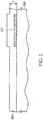
- FIGs. 2-8 are schematic cross sections showing a method for forming a Wafer-level chip scale package (WLCSP) having a structure with a reduced size, according to another embodiment of the present disclosure.
- WLCSP Wafer-level chip scale package
- a semiconductor structure 200 having a bonding pad 202 formed over a portion of the semiconductor structure 200 is provided.
- a passivation layer 204 is conformably formed over the semiconductor structure 200 and the first bonding pad 204 by, for example, a chemical vapor deposition (CVD) process (not shown). Since the passivation layer 204 is conformably formed over the semiconductor structure 200 and the first bonding pad 202, the passivation layer 204 has a non-flat top surface over the semiconductor structure 200.
- the portion of the passivation layer 204 formed over the semiconductor structure 200 has a thickness T of about 1 ⁇ m to about 6 ⁇ m.
- the semiconductor structure 200 is the same as the semiconductor structure 100 shown in FIG. 1 , and the passivation layer 204 and the bonding pad 202 are respectively the same as those used for forming the passivation layer 104 and the bonding pad 102 shown in FIG. 1 .
- a planarization process 206 is performed to level a top surface of the passivation layer 204 and reduce the thickness of the passivation layer 204, thereby leaving a passivation layer 204a having a flat top surface over both the semiconductor structure 200 and the bonding pad 202.
- the passivation layer 204a has a reduced thickness T' of about 1 ⁇ m to about 6 ⁇ m above the semiconductor structure 200.
- the planarization process 206 can be a chemical mechanical polishing (CMP) process, for example, or an etching back process.
- a patterning process 208 is next performed on the passivation layer 204a shown in FIG. 3 to form a plurality of openings 210 only in portions of the passivation layer 204a over the bonding pad 202. Therefore, a plurality of portions of the bonding pad 202 is exposed by the openings 210.
- Each of the openings 210 has a dimension W, for example a width, of about 2 ⁇ m or above, and the openings 210 may have a circular, stripe-like, or polygonal shape from a top view (not shown).
- the patterning process 208 may comprise photolithography and etching steps (not shown) with suitable patterned masks (not shown) used as an etching mask.
- a patterned conductive redistribution layer 212 is next formed over portions of the passivation layer 204a over the bonding pad 202.
- the patterned conductive redistribution layer 212 comprises a plurality of first portions 212a filling the openings 210 formed in the passivation layer 204a, and a second portion 212b formed above the flat top surface of the passivation layer 204a and the openings 210. Therefore, the patterned conductive redistribution layer 212 is also provided with a substantially flat top surface, as shown in FIG. 5 .
- the patterned conductive redistribution layer 212 can be formed by first forming a conductive redistribution layer 212 over the passivation layer 204a and in the openings 210, and then the conductive redistribution layer 212 is patterned by a patterning process (not shown) comprising photolithography and etching steps (not shown) incorporating suitable patterned masks (not shown) as an etching mask.
- Conductive materials for forming the patterned conductive redistribution layer 212 can be the same as those of the conductive redistribution layer 110 shown in FIG. 1 , with a thickness of about 4 ⁇ m to about 9 ⁇ m above the passivation layer 204a.
- a planarization layer 214 is formed over the top surface of the structure shown in FIG. 5 , and an opening 216 is then formed in a portion of the planarization layer 214 to expose a portion of the patterned conductive redistribution layer 212.
- the planarization layer 214 can be formed by a chemical vapor deposition (CVD) or spin coating process, for example, and may be patterned by a patterning process (not shown) comprising photolithography and etching steps (not shown) incorporating suitable patterned masks (not shown) as an etching mask.
- Materials for forming the planarization layer 214 can be the same as those of the first planarization layer 112 shown in FIG. 1 , and the planarization layer 214 may have a thickness of about 7.5 ⁇ m to about 10 ⁇ m, which is greater than the thickness of the patterned conductive redistribution layer 212.
- an under-bump-metallurgy (UBM) layer 218 is next formed over the portion of the patterned conductive redistribution layer 212 exposed by the opening 216 and portions of the planarization layer 214 adjacent to the opening 216.
- the UBM layer 218 can be formed by forming a layer of conductive material over the structure shown in FIG. 6 by, for example, a chemical vapor deposition (CVD) or electrical plating process, and is then patterned by a patterning process (not shown) comprising photolithography and etching steps (not shown) incorporating suitable patterned masks (not shown) as an etching mask.
- Materials for forming the UBM layer 218 can be the same as that of the UBM layer 116 shown in FIG. 1 , and the UBM layer 218 may have a thickness of about 4 ⁇ m to about 9 ⁇ m.
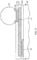
- a conductive bump 220 is next formed over the UBM layer 218 by conventional solder bump formation processes. Since the patterned conductive redistribution layer 212 is now provided with a substantially flat top surface rather than a step-like configuration, the UBM layer 218 and the conductive bump 220 can be sequentially and firmly formed over the patterned conductive redistribution layer 212. In addition, since the patterned conductive redistribution layer 212 is formed directly over the bonding pad 202, the conductive bump 220 and the UBM layer 218 are also formed directly over the bond pad 202, so that a bonding structure for the WLCSP with a reduced size can be obtained.
- the WLCSP in FIG. 8 can be fabricated more easily than the WLCSP shown in FIG. 1 , which utilizes two planarization layers.
- FIG. 9 is a schematic cross section showing another exemplary Wafer-level chip scale package (WLCSP) of the present disclosure.
- WLCSP Wafer-level chip scale package
- the second portion 212b of the patterned conductive redistribution layer 212 having a flat top surface is not only formed over the bonding pad 202 as shown in FIG. 8 , but it further extends over a portion of the passivation layer 204a not covering the bonding pad 202 to thereby provide a line-routing function, so that the UBM layer 218 and the conductive bump 220 can thus be formed over a portion of the second portion 212b of the patterned conductive redistribution layer 212 at a place that is not covering the bonding pad 202.
- the WLCSP in FIG. 9 can also be fabricated more easily than the WLCSP shown in FIG. 1 , which utilizes two planarization layers.
- FIG. 10 is a schematic cross section showing another exemplary Wafer-level chip scale package (WLCSP) of the present disclosure.
- WLCSP Wafer-level chip scale package
- the semiconductor structure 200 is now provided with two isolated bonding pads 202 formed thereover, and configurations of the passivation layer 204a and the openings 210 formed in the passivation layer 204a are the same at a place over each of the bonding pads 202.
- the patterned conductive redistribution layer 212 has a first portion 212a formed in the openings 210 which are formed over each of the passivation layers 204a over the bonding pads 202 and a second portion 212b over the leveled passivation layer 204a between the bonding pads 202.
- the UBM layer 218 and the conductive bump 220 are formed over a portion of the second portion 212b of the conductive redistribution layer 212 over one of the bonding pads 202.
- the patterned conductive redistribution layer 212 is now provided with a substantially flat top surface, so the UBM layer 218 and the conductive bump 220 can thus be formed firmly over the patterned conductive redistribution layer 212.
- the patterned conductive redistribution layer 212 is formed directly over the bonding pad 202, the conductive bump 220 and the UBM layer 218 are also formed directly over one of the bond pads 202, so that a bonding structure for the WLCSP with a reduced size can be obtained.
- the WLCSP in FIG. 9 can be fabricated more easily than the WLCSP shown in FIG. 1 , which utilizes two planarization layers.
Landscapes
- Internal Circuitry In Semiconductor Integrated Circuit Devices (AREA)
Abstract
Description
- This application claims the benefit of
U.S. Provisional Application No. 62/262,420 filed December 3, 2015 - The present invention relates to integrated circuits (ICs), and in particular to a wafer-level chip scale package (WLCSP) with a redistribution layer and a method of manufacturing the same.
- The desire to make electronic products small, lightweight, and high-performing has developed into a desire to make electronic parts small, lightweight, and high-performing. This desire has caused developments to proceed in various packaging technologies, along with developments in the technologies related to designing and manufacturing semiconductors. Representative examples of packaging technologies include the ball grid array (BGA), the flip-chip, and the chip scale package (CSP) based on area array and surface-mount packaging.
- Among the above, the CSP is a packaging technology that enables a small package to be the same size as the real chip to be developed. In particular, in a Wafer-level chip scale package (WLCSP), the packaging is performed in a wafer level so that the packaging costs per chip can be remarkably reduced. Typically, the WLCSP includes a redistribution layer (RDL) wiring traces, an under bump metallurgy (UBM) layer forming a bump, and a passivation layer protecting a circuit.
- An exemplary Wafer-level chip scale package (WLCSP) comprises a semiconductor structure and a first bonding pad formed over a portion of the semiconductor structure. The WLCSP further comprises a passivation layer formed over the semiconductor structure and the first bonding pad, wherein the passivation layer exposes a plurality of portions of the first bonding pad. The WLCSP further comprises a conductive redistribution layer formed over the passivation layer and the portions of the first bonding pad exposed by the passivation layer. The WLCSP further comprises a planarization layer formed over the passivation layer and the conductive redistribution layer, exposing a portion of the conductive redistribution layer. The WLCSP further comprises an under bump-metallurgy (UBM) layer formed over the planarization layer and the portion of the conductive redistribution layer exposed by the planarization layer. The WLCSP further comprises a conductive bump formed over the UBM layer.
- An exemplary method for forming a Wafer-level chip scale package (WLCSP) comprises providing a semiconductor structure having a first bonding pad formed over the semiconductor structure and forming a passivation layer over the semiconductor structure and the first bonding pad, wherein the passivation layer exposes a plurality of portions of the first bonding pad. The method further comprises forming a conductive redistribution layer over the passivation layer and the portions of the first bonding pad exposed by the passivation layer, and forming a planarization layer over the passivation layer and the conductive redistribution layer, exposing a portion of the conductive redistribution layer. The method further comprises forming an under-bump-metallurgy (UBM) layer over the portion of the portion of the conductive redistribution layer exposed by the planarization layer, and forming a conductive bump formed over the UBM layer.
- A detailed description is given in the following embodiments with reference to the accompanying drawings.
- The invention can be more fully understood by reading the subsequent detailed description and examples with references made to the accompanying drawings, wherein:
-
FIG. 1 is a schematic cross section showing a Wafer-level chip scale package (WLCSP) according to an embodiment of the present disclosure; -
FIGs. 2-8 are a schematic cross sections showing a method for forming a Wafer-level chip scale package (WLCSP) according to an embodiment of the present disclosure; -
FIG. 9 is a schematic cross section showing a Wafer-level chip scale package (WLCSP) according to another embodiment of the present disclosure; and -
FIG. 10 is a schematic cross section showing a Wafer-level chip scale package (WLCSP) according to yet another embodiment of the present disclosure. - The following description is of the best-contemplated mode of carrying out the invention. This description is made for the purpose of illustrating the general principles of the invention and should not be taken in a limiting sense. The scope of the invention is best determined by reference to the appended claims.
-
FIG. 1 is a schematic cross section showing a Wafer-level chip scale package (WLCSP) according to an embodiment of the present disclosure. - As shown in
FIG. 1 , the WLCSP comprises a semiconductor structure 100, abonding pad 102, apassivation layer 104, afirst planarization layer 106, asecond planarization layer 112, aconductive redistribution layer 110, an under-bump-metallurgy (UBM)layer 116, and aconductive bump 118. - Herein, the semiconductor structure 100 is illustrated as a structure having a flat top surface for the purpose of simplifying the figure. It should be noted that the semiconductor structure 100 can be a wafer-level semiconductor substrate having a plurality of semiconductor devices and interconnect structures (both not shown) formed thereon. The semiconductor devices formed over the semiconductor structure 100 can be, for example, active devices such as transistors or diodes and/or passive devices such as capacitors, resistors and conductors. The interconnect structures in the semiconductor structure 100 may comprise a multi-layer metallization structure isolated and supported by a plurality of interlayer dielectric layers. In this embodiment, only a portion of the semiconductor structure 100 is illustrated as the WLCSP.
- Referring to
FIG. 1 , thebonding pad 102 is formed over a portion of the semiconductor structure 100 and may be electrically connected with one of the interconnect structure (not shown) of a circuit formed in the semiconductor structure 100. Thepassivation layer 104 and thefirst planarization layer 106 are sequentially formed over the semiconductor structure 100, and thepassivation layer 104 and thefirst planarization layer 106 partially respectively cover portions of thebonding pad 102. Anopening 108 is formed in thefirst planarization layer 106 to expose a portion of thebonding pad 102, and theconductive redistribution layer 110 is conformably formed over portions of thefirst planarization layer 106 and in the opening to cover the portion of thebonding pad 102 exposed by theopening 108. Thesecond planarization layer 112 is formed over thefirst planarization layer 106 and theconductive redistribution layer 110, and anopening 116 is formed in thesecond planarization layer 112 to expose a portion of theconductive redistribution layer 110. TheUBM layer 116 is formed over a portion of thesecond planarization layer 112 and the portion of theconductive redistribution layer 110 exposed by thesecond planarization layer 112, and theconductive bump 118 is formed over theUBM layer 116. - In this embodiment, the
bonding pad 102 may comprise conductive materials such as aluminum, and thepassivation layer 104 may comprise dielectric materials such as silicon oxide, silicon nitride, or combination thereof. Thefirst planarization layer 106 and thesecond planarization layer 108 may comprise dielectric materials such as silicon nitride, silicon oxide, or polymer. In one embodiment, the polymer suitable for thefirst planarization layer 106 and thesecond planarization layer 108 can be, for example, polyimide, polybenzoxazole, or benzocyclobutene. Theconductive redistribution layer 110 may comprise conductive materials such as copper, nickel, or aluminum. TheUBM layer 116 may comprise conductive materials such as metals or metal alloys such as Ni layers, Ag layers, A1 layers, Cu layers or alloys thereof, or materials of doped polysilicon, monocrystalline silicon or conductive glasses. Additionally, refractory metal materials such as titanium, molybdenum, chromium or titanium tungsten layers can be used to individually form the UBM layers or be combined with other metal layers. Typically, thefist passivation layer 106 is provided with a thickness C of about 5 µm to about 7.5 µm, and a step-height of the first planarization layer over thebonding pad 102 is too large, such that opening 108 formed in thefirst planarization layer 106 is a single opening of a greater dimension of, for example, about 22 µm to about 30 µm. Therefore, theconductive redistribution layer 110 is conformably formed over portions of thefirst planarization layer 106 and the portion of thebonding pad 102 exposed by theopening 108 and has a step portion A of a step-like configuration near theopening 108 and a flat portion B of a flat configuration extending from the opening 114 and over thefirst planarization layer 106. In addition, theopening 114 formed in thesecond planarization layer 112 exposes a portion of the planar portion B of theconductive redistribution layer 110, such that theUBM layer 116 can be conformably disposed over portions of thesecond planarization layer 112 and the planar portion B of theconductive redistribution layer 110 exposed by theopening 114. - In the WLCSP shown in
FIG. 1 , since thefirst planarization layer 106 is provided, and it has a thickness C of about 5 µm to about 7.5 µm, the step-height of thefirst planarization layer 106 near theopening 108 is too large to make theopening 108 smaller. Thus, the portion of theconductive redistribution layer 110 near theopening 108 is formed with a step-like configuration, and theUBM layer 116 and thesolder bump 118 formed over the UBM layer only can be formed over the planar portion B of theconductive redistribution layer 110 extending from theopening 108 and over thefirst passivation layer 106. Therefore, the footprint of the WLCSP shown inFIG. 1 is quite large, which is undesirable because of the trend towards further reduction in the size of the integrated circuits in the WLCSP. - Therefore,
FIGs. 2-8 are schematic cross sections showing a method for forming a Wafer-level chip scale package (WLCSP) having a structure with a reduced size, according to another embodiment of the present disclosure. - Referring to
FIG. 2 , asemiconductor structure 200 having abonding pad 202 formed over a portion of thesemiconductor structure 200 is provided. Next, apassivation layer 204 is conformably formed over thesemiconductor structure 200 and thefirst bonding pad 204 by, for example, a chemical vapor deposition (CVD) process (not shown). Since thepassivation layer 204 is conformably formed over thesemiconductor structure 200 and thefirst bonding pad 202, thepassivation layer 204 has a non-flat top surface over thesemiconductor structure 200. In one embodiment, the portion of thepassivation layer 204 formed over thesemiconductor structure 200 has a thickness T of about 1 µm to about 6 µm. - In one embodiment, the
semiconductor structure 200 is the same as the semiconductor structure 100 shown inFIG. 1 , and thepassivation layer 204 and thebonding pad 202 are respectively the same as those used for forming thepassivation layer 104 and thebonding pad 102 shown inFIG. 1 . - Referring to
FIG. 3 , aplanarization process 206 is performed to level a top surface of thepassivation layer 204 and reduce the thickness of thepassivation layer 204, thereby leaving apassivation layer 204a having a flat top surface over both thesemiconductor structure 200 and thebonding pad 202. At this time, thepassivation layer 204a has a reduced thickness T' of about 1 µm to about 6 µm above thesemiconductor structure 200. Theplanarization process 206 can be a chemical mechanical polishing (CMP) process, for example, or an etching back process. - Referring to
FIG. 4 , apatterning process 208 is next performed on thepassivation layer 204a shown inFIG. 3 to form a plurality ofopenings 210 only in portions of thepassivation layer 204a over thebonding pad 202. Therefore, a plurality of portions of thebonding pad 202 is exposed by theopenings 210. Each of theopenings 210 has a dimension W, for example a width, of about 2 µm or above, and theopenings 210 may have a circular, stripe-like, or polygonal shape from a top view (not shown). In one embodiment, thepatterning process 208 may comprise photolithography and etching steps (not shown) with suitable patterned masks (not shown) used as an etching mask. - Referring to
FIG. 5 , a patternedconductive redistribution layer 212 is next formed over portions of thepassivation layer 204a over thebonding pad 202. As shown inFIG. 5 , the patternedconductive redistribution layer 212 comprises a plurality offirst portions 212a filling theopenings 210 formed in thepassivation layer 204a, and asecond portion 212b formed above the flat top surface of thepassivation layer 204a and theopenings 210. Therefore, the patternedconductive redistribution layer 212 is also provided with a substantially flat top surface, as shown inFIG. 5 . The patternedconductive redistribution layer 212 can be formed by first forming aconductive redistribution layer 212 over thepassivation layer 204a and in theopenings 210, and then theconductive redistribution layer 212 is patterned by a patterning process (not shown) comprising photolithography and etching steps (not shown) incorporating suitable patterned masks (not shown) as an etching mask. Conductive materials for forming the patternedconductive redistribution layer 212 can be the same as those of theconductive redistribution layer 110 shown inFIG. 1 , with a thickness of about 4 µm to about 9 µm above thepassivation layer 204a. - Referring to
FIG. 6 , aplanarization layer 214 is formed over the top surface of the structure shown inFIG. 5 , and anopening 216 is then formed in a portion of theplanarization layer 214 to expose a portion of the patternedconductive redistribution layer 212. Theplanarization layer 214 can be formed by a chemical vapor deposition (CVD) or spin coating process, for example, and may be patterned by a patterning process (not shown) comprising photolithography and etching steps (not shown) incorporating suitable patterned masks (not shown) as an etching mask. Materials for forming theplanarization layer 214 can be the same as those of thefirst planarization layer 112 shown inFIG. 1 , and theplanarization layer 214 may have a thickness of about 7.5 µm to about 10 µm, which is greater than the thickness of the patternedconductive redistribution layer 212. - Referring to
FIG. 7 , an under-bump-metallurgy (UBM)layer 218 is next formed over the portion of the patternedconductive redistribution layer 212 exposed by theopening 216 and portions of theplanarization layer 214 adjacent to theopening 216. TheUBM layer 218 can be formed by forming a layer of conductive material over the structure shown inFIG. 6 by, for example, a chemical vapor deposition (CVD) or electrical plating process, and is then patterned by a patterning process (not shown) comprising photolithography and etching steps (not shown) incorporating suitable patterned masks (not shown) as an etching mask. Materials for forming theUBM layer 218 can be the same as that of theUBM layer 116 shown inFIG. 1 , and theUBM layer 218 may have a thickness of about 4 µm to about 9 µm. - Referring to
FIG. 8 , aconductive bump 220 is next formed over theUBM layer 218 by conventional solder bump formation processes. Since the patternedconductive redistribution layer 212 is now provided with a substantially flat top surface rather than a step-like configuration, theUBM layer 218 and theconductive bump 220 can be sequentially and firmly formed over the patternedconductive redistribution layer 212. In addition, since the patternedconductive redistribution layer 212 is formed directly over thebonding pad 202, theconductive bump 220 and theUBM layer 218 are also formed directly over thebond pad 202, so that a bonding structure for the WLCSP with a reduced size can be obtained. - In addition, since there is only one
planarization layer 214 utilized in the WLCSP shown inFIG. 8 , the WLCSP inFIG. 8 can be fabricated more easily than the WLCSP shown inFIG. 1 , which utilizes two planarization layers. - In addition to the exemplary embodiment shown in
FIG. 8 ,FIG. 9 is a schematic cross section showing another exemplary Wafer-level chip scale package (WLCSP) of the present disclosure. At this time, the WLCSP shown inFIG. 9 is modified from the WLCSP shown inFIG. 8 , and similar components inFIG. 9 are represented with the same reference numbers shown inFIG. 8 , and only differences between the WLCSPs shown inFIGs. 8-9 are discussed as below. - Referring to
FIG. 9 , thesecond portion 212b of the patternedconductive redistribution layer 212 having a flat top surface is not only formed over thebonding pad 202 as shown inFIG. 8 , but it further extends over a portion of thepassivation layer 204a not covering thebonding pad 202 to thereby provide a line-routing function, so that theUBM layer 218 and theconductive bump 220 can thus be formed over a portion of thesecond portion 212b of the patternedconductive redistribution layer 212 at a place that is not covering thebonding pad 202. Similarly, since there is only oneplanarization layer 214 utilized in the WLCSP shown inFIG. 9 , the WLCSP inFIG. 9 can also be fabricated more easily than the WLCSP shown inFIG. 1 , which utilizes two planarization layers. - In addition to the exemplary embodiment shown in
FIG. 9 ,FIG. 10 is a schematic cross section showing another exemplary Wafer-level chip scale package (WLCSP) of the present disclosure. At this time, the WLCSP shown inFIG. 10 is modified from the WLCSP shown inFIG. 9 , and similar components shown inFIG. 10 are represented with the same reference numbers, and only differences between the WLCSPs shown inFIGs. 9-10 are discussed as below. - Referring to
FIG. 10 , thesemiconductor structure 200 is now provided with twoisolated bonding pads 202 formed thereover, and configurations of thepassivation layer 204a and theopenings 210 formed in thepassivation layer 204a are the same at a place over each of thebonding pads 202. In this embodiment, the patternedconductive redistribution layer 212 has afirst portion 212a formed in theopenings 210 which are formed over each of thepassivation layers 204a over thebonding pads 202 and asecond portion 212b over the leveledpassivation layer 204a between thebonding pads 202. TheUBM layer 218 and theconductive bump 220 are formed over a portion of thesecond portion 212b of theconductive redistribution layer 212 over one of thebonding pads 202. - Similarly, the patterned
conductive redistribution layer 212 is now provided with a substantially flat top surface, so theUBM layer 218 and theconductive bump 220 can thus be formed firmly over the patternedconductive redistribution layer 212. In addition, since the patternedconductive redistribution layer 212 is formed directly over thebonding pad 202, theconductive bump 220 and theUBM layer 218 are also formed directly over one of thebond pads 202, so that a bonding structure for the WLCSP with a reduced size can be obtained. - Moreover, since there is only one
planarization layer 214 utilized in the WLCSP shown inFIG. 10 , the WLCSP inFIG. 9 can be fabricated more easily than the WLCSP shown inFIG. 1 , which utilizes two planarization layers. - While the invention has been described by way of example and in terms of the preferred embodiments, it should be understood that the invention is not limited to the disclosed embodiments. On the contrary, it is intended to cover various modifications and similar arrangements (as would be apparent to those skilled in the art). Therefore, the scope of the appended claims should be accorded the broadest interpretation so as to encompass all such modifications and similar arrangements.
Claims (15)
- A wafer-level chip-scale package, comprising:a semiconductor structure;a first bonding pad formed over a portion of the semiconductor structure;a passivation layer formed over the semiconductor structure and the first bonding pad, wherein the passivation layer exposes a plurality of portions of the first bonding pad;a conductive redistribution layer formed over the passivation layer and the portions of the first bonding pad exposed by the passivation layer;a planarization layer formed over the passivation layer and the conductive redistribution layer, exposing a portion of the conductive redistribution layer;an under-bump-metallurgy (UBM) layer formed over the planarization layer and the portion of the conductive redistribution layer exposed by the planarization layer; anda conductive bump formed over the UBM layer.
- The Wafer-level chip-scale package claimed in claim 1, wherein the passivation layer formed over the semiconductor structure and the first bonding pad has a flat top surface.
- The Wafer-level chip-scale package claimed in claim 1 or 2, wherein the conductive redistribution layer formed over the portions of the first bonding pad exposed by the passivation layer has a substantially flat top surface, and/or
wherein the passivation comprises dielectric materials. - The Wafer-level chip-scale package claimed in one of the previous claims, wherein the planarization layer comprises polyimide, polybenzoxazole or benzocyclobutene.
- The Wafer-level chip-scale package claimed in one of the previous claims, wherein the UBM layer is formed over a portion of the conductive redistribution layer at a place over the portions of the first bonding pad exposed by the passivation layer.
- The Wafer-level chip-scale package claimed in one of claims 1 to 4, wherein the UBM layer is formed over the portion of the conductive redistribution layer at a place that is not over the portions of the first bonding pad exposed by the passivation layer.
- The Wafer-level chip-scale package claimed in one of the previous claims, wherein the portions of the first bonding pad exposed by the passivation layer respectively have a dimension of about 2 µm or above from a top view, and/or
wherein the portions of the first bonding pad exposed by the passivation layer respectively have a circular, stripe-like, or polygonal shape. - The Wafer-level chip-scale package claimed in one of the previous claims, further comprising a second bonding pad formed over another portion of the semiconductor structure,
wherein the passivation layer is preferably formed over the second bonding pad and exposes a plurality of portions of the second bonding pad,
wherein the conductive redistribution layer is preferably formed over the portions of the second bonding pad exposed by the passivation layer and has a substantially flat top surface,
wherein the UBM layer is preferably formed over a portion of the conductive redistribution layer at a place over the portions of the first bonding pad exposed by the passivation layer or portions of the second bonding pad exposed by the passivation layer. - A method for forming a wafer-level chip-scale package, comprising:providing a semiconductor structure having a first bonding pad formed over the semiconductor structure;forming a passivation layer over the semiconductor structure and the first bonding pad, wherein the passivation layer exposes a plurality of portions of the first bonding pad;forming a conductive redistribution layer over the passivation layer and the portions of the first bonding pad exposed by the passivation layer;forming a planarization layer over the passivation layer and the conductive redistribution layer, exposing a portion of the conductive redistribution layer;forming an under-bump-metallurgy (UBM) layer over the portion of the portion of the conductive redistribution layer exposed by the planarization layer; andforming a conductive bump formed over the UBM layer.
- The method as claimed in claim 9, wherein formation of the passivation layer over the semiconductor structure and the first bonding pad comprises:conformably forming the passivation layer over the semiconductor structure and the first bonding pad;performing a planarization process and removing a portion of the passivation layer over the first bonding pad, thereby leveling a top surface of the passivation layer over the semiconductor structure and the first bonding pad; andafter the planarization process, forming a plurality of first openings in the passivation layer and exposing the plurality of portions of the first bonding pad.
- The method as claimed in claim 9 or 10, wherein formation of the planarization layer over the passivation layer and the conductive redistribution layer to expose a portion of the conductive redistribution layer comprises:forming the planarization layer formed over the passivation layer and the conductive redistribution layer; andforming an opening in a portion of the planarization layer and exposing the portion of the conductive redistribution layer.
- The method as claimed in one of claims 9 to 11, wherein the passivation layer formed over the semiconductor structure and the first bonding pad has a flat top surface, and/or
wherein the conductive redistribution layer formed over the portions of the first bonding pad exposed by the passivation layer has a substantially flat top surface, and/or
wherein the portions of the first bonding pad exposed by the passivation layer respectively have a dimension of about 2 µm or above from a top view. - The method as claimed in claim 14, wherein the portions of the first bonding pad exposed by the passivation layer respectively have a circular, stripe-like, or polygonal shape, and/or
further providing a second bonding pad over another portion of the semiconductor structure. - The method as claimed in one of claims 9 to 13, wherein the passivation layer is also formed over the second bonding pad and exposes a plurality of portions of the second bonding pad,
wherein the conductive redistribution layer is preferably formed over the portions of the second bonding pad exposed by the passivation layer, having a substantially flat top surface, and/or
wherein the UBM layer is preferably formed over a portion of the conductive redistribution layer formed over the portions of the first bonding pad exposed by the passivation layer or the portions of the second bonding pad exposed by the passivation layer. - The method as claimed in one of claims 9 to 14, wherein the passivation comprises dielectric materials, and the planarization layer comprises polyimide, polybenzoxazole or benzocyclobutene.
Applications Claiming Priority (2)
| Application Number | Priority Date | Filing Date | Title |
|---|---|---|---|
| US201562262420P | 2015-12-03 | 2015-12-03 | |
| US15/274,506 US9953954B2 (en) | 2015-12-03 | 2016-09-23 | Wafer-level chip-scale package with redistribution layer |
Publications (2)
| Publication Number | Publication Date |
|---|---|
| EP3176819A2 true EP3176819A2 (en) | 2017-06-07 |
| EP3176819A3 EP3176819A3 (en) | 2017-06-28 |
Family
ID=57391817
Family Applications (1)
| Application Number | Title | Priority Date | Filing Date |
|---|---|---|---|
| EP16199908.1A Withdrawn EP3176819A3 (en) | 2015-12-03 | 2016-11-22 | Wafer-level chip-scale package with redistribution layer |
Country Status (4)
| Country | Link |
|---|---|
| US (1) | US9953954B2 (en) |
| EP (1) | EP3176819A3 (en) |
| CN (1) | CN107026138A (en) |
| TW (1) | TW201731043A (en) |
Cited By (1)
| Publication number | Priority date | Publication date | Assignee | Title |
|---|---|---|---|---|
| CN113053845A (en) * | 2019-12-27 | 2021-06-29 | 意法半导体有限公司 | WLCSP package with different solder volumes |
Families Citing this family (18)
| Publication number | Priority date | Publication date | Assignee | Title |
|---|---|---|---|---|
| US9741651B1 (en) * | 2016-02-24 | 2017-08-22 | Intel IP Corportaion | Redistribution layer lines |
| US9984987B2 (en) * | 2016-08-05 | 2018-05-29 | Nanya Technology Corporation | Semiconductor structure and manufacturing method thereof |
| US10515913B2 (en) * | 2017-03-17 | 2019-12-24 | Invensas Bonding Technologies, Inc. | Multi-metal contact structure |
| US10553527B2 (en) * | 2017-09-12 | 2020-02-04 | Advanced Semiconductor Engineering, Inc. | Substrate and semiconductor device package |
| CN107768343A (en) * | 2017-09-29 | 2018-03-06 | 江苏长电科技股份有限公司 | High reliability RDL stacks open-celled structure |
| US11364493B2 (en) | 2017-10-12 | 2022-06-21 | Hewlett-Packard Development Company, L.P. | Planarization layers over silicon dies |
| US10083926B1 (en) * | 2017-12-13 | 2018-09-25 | Dialog Semiconductor (Uk) Limited | Stress relief solutions on WLCSP large/bulk copper plane design |
| US10896887B2 (en) * | 2018-05-10 | 2021-01-19 | Infineon Technologies Ag | Stress relieving structure for semiconductor device |
| KR102543186B1 (en) * | 2018-11-23 | 2023-06-14 | 삼성전자주식회사 | Semiconductor package |
| US11373968B2 (en) * | 2019-04-26 | 2022-06-28 | Cirrus Logic, Inc. | Via structure for semiconductor dies |
| KR102499476B1 (en) * | 2019-08-19 | 2023-02-13 | 삼성전자주식회사 | Semiconductor package |
| US12057417B2 (en) * | 2019-10-15 | 2024-08-06 | Texas Instruments Incorporated | Wafer chip scale package |
| CN110729179A (en) * | 2019-10-30 | 2020-01-24 | 华虹半导体(无锡)有限公司 | Processing method of smart card chip and smart card chip |
| CN112542378B (en) * | 2020-12-01 | 2024-03-26 | 武汉新芯集成电路制造有限公司 | Method for manufacturing semiconductor device and semiconductor device |
| CN113990759B (en) * | 2020-12-21 | 2025-07-22 | 矽磐微电子(重庆)有限公司 | Semiconductor packaging method and semiconductor packaging structure |
| US11935852B2 (en) * | 2021-04-08 | 2024-03-19 | Mediatek Inc. | Semiconductor package and manufacturing method thereof |
| CN114068465B (en) * | 2021-11-04 | 2025-08-29 | 华进半导体封装先导技术研发中心有限公司 | A redistribution layer structure and construction method thereof |
| CN114823556A (en) * | 2022-03-29 | 2022-07-29 | 成都奕斯伟系统技术有限公司 | Semiconductor package and method of forming the same |
Family Cites Families (17)
| Publication number | Priority date | Publication date | Assignee | Title |
|---|---|---|---|---|
| JP2974022B1 (en) * | 1998-10-01 | 1999-11-08 | ヤマハ株式会社 | Bonding pad structure of semiconductor device |
| JP3685722B2 (en) | 2001-02-28 | 2005-08-24 | 三洋電機株式会社 | Semiconductor device and manufacturing method thereof |
| JP4360873B2 (en) | 2003-09-18 | 2009-11-11 | ミナミ株式会社 | Manufacturing method of wafer level CSP |
| JP2005243907A (en) * | 2004-02-26 | 2005-09-08 | Renesas Technology Corp | Semiconductor device |
| US7364998B2 (en) * | 2005-07-21 | 2008-04-29 | Taiwan Semiconductor Manufacturing Co., Ltd. | Method for forming high reliability bump structure |
| US8319343B2 (en) * | 2005-09-21 | 2012-11-27 | Agere Systems Llc | Routing under bond pad for the replacement of an interconnect layer |
| US7952206B2 (en) * | 2005-09-27 | 2011-05-31 | Agere Systems Inc. | Solder bump structure for flip chip semiconductor devices and method of manufacture therefore |
| KR100804392B1 (en) | 2005-12-02 | 2008-02-15 | 주식회사 네패스 | Semiconductor package and manufacturing method thereof |
| JP4998270B2 (en) * | 2005-12-27 | 2012-08-15 | 富士通セミコンダクター株式会社 | Semiconductor device and manufacturing method thereof |
| JP4818005B2 (en) | 2006-07-14 | 2011-11-16 | Okiセミコンダクタ株式会社 | Semiconductor device and manufacturing method thereof |
| CN101882608B (en) * | 2009-05-08 | 2012-05-30 | 台湾积体电路制造股份有限公司 | Bump pad structure and manufacturing method thereof |
| US9105588B2 (en) * | 2010-10-21 | 2015-08-11 | Taiwan Semiconductor Manufacturing Company, Ltd. | Semiconductor component having a second passivation layer having a first opening exposing a bond pad and a plurality of second openings exposing a top surface of an underlying first passivation layer |
| TW201304098A (en) | 2011-07-01 | 2013-01-16 | 力成科技股份有限公司 | Wafer-level wafer size package wire bonding structure and process thereof |
| JP2016129161A (en) | 2013-04-24 | 2016-07-14 | パナソニック株式会社 | Semiconductor device |
| US20150228594A1 (en) | 2014-02-13 | 2015-08-13 | Qualcomm Incorporated | Via under the interconnect structures for semiconductor devices |
| US9318429B2 (en) | 2014-03-31 | 2016-04-19 | Taiwan Semiconductor Manufacturing Company, Ltd. | Integrated structure in wafer level package |
| US20160086960A1 (en) * | 2014-09-22 | 2016-03-24 | Texas Instruments Incorporated | Low-Temperature Passivation of Ferroelectric Integrated Circuits for Enhanced Polarization Performance |
-
2016
- 2016-09-23 US US15/274,506 patent/US9953954B2/en active Active
- 2016-11-22 EP EP16199908.1A patent/EP3176819A3/en not_active Withdrawn
- 2016-11-29 TW TW105139207A patent/TW201731043A/en unknown
- 2016-12-01 CN CN201611091100.5A patent/CN107026138A/en active Pending
Non-Patent Citations (1)
| Title |
|---|
| None |
Cited By (1)
| Publication number | Priority date | Publication date | Assignee | Title |
|---|---|---|---|---|
| CN113053845A (en) * | 2019-12-27 | 2021-06-29 | 意法半导体有限公司 | WLCSP package with different solder volumes |
Also Published As
| Publication number | Publication date |
|---|---|
| EP3176819A3 (en) | 2017-06-28 |
| US20170162540A1 (en) | 2017-06-08 |
| TW201731043A (en) | 2017-09-01 |
| US9953954B2 (en) | 2018-04-24 |
| CN107026138A (en) | 2017-08-08 |
Similar Documents
| Publication | Publication Date | Title |
|---|---|---|
| US9953954B2 (en) | Wafer-level chip-scale package with redistribution layer | |
| US11784124B2 (en) | Plurality of different size metal layers for a pad structure | |
| US10998267B2 (en) | Wafer-level chip-size package with redistribution layer | |
| US9659890B2 (en) | Methods and apparatus of packaging semiconductor devices | |
| US9741659B2 (en) | Electrical connections for chip scale packaging | |
| US9349665B2 (en) | Methods and apparatus of packaging of semiconductor devices | |
| US9093333B1 (en) | Integrated circuit device having extended under ball metallization | |
| US10269749B2 (en) | Method of forming a semiconductor device with bump stop structure | |
| US20110266670A1 (en) | Wafer level chip scale package with annular reinforcement structure | |
| US11393771B2 (en) | Bonding structures in semiconductor packaged device and method of forming same | |
| US20090200675A1 (en) | Passivated Copper Chip Pads | |
| US20130087892A1 (en) | Electrical Connection for Chip Scale Packaging | |
| US9997482B2 (en) | Solder stud structure | |
| US7176117B2 (en) | Method for mounting passive components on wafer |
Legal Events
| Date | Code | Title | Description |
|---|---|---|---|
| PUAL | Search report despatched |
Free format text: ORIGINAL CODE: 0009013 |
|
| AK | Designated contracting states |
Kind code of ref document: A2 Designated state(s): AL AT BE BG CH CY CZ DE DK EE ES FI FR GB GR HR HU IE IS IT LI LT LU LV MC MK MT NL NO PL PT RO RS SE SI SK SM TR |
|
| AX | Request for extension of the european patent |
Extension state: BA ME |
|
| PUAI | Public reference made under article 153(3) epc to a published international application that has entered the european phase |
Free format text: ORIGINAL CODE: 0009012 |
|
| RIC1 | Information provided on ipc code assigned before grant |
Ipc: H01L 23/31 20060101AFI20170518BHEP |
|
| AK | Designated contracting states |
Kind code of ref document: A3 Designated state(s): AL AT BE BG CH CY CZ DE DK EE ES FI FR GB GR HR HU IE IS IT LI LT LU LV MC MK MT NL NO PL PT RO RS SE SI SK SM TR |
|
| AX | Request for extension of the european patent |
Extension state: BA ME |
|
| 17P | Request for examination filed |
Effective date: 20171214 |
|
| RBV | Designated contracting states (corrected) |
Designated state(s): AL AT BE BG CH CY CZ DE DK EE ES FI FR GB GR HR HU IE IS IT LI LT LU LV MC MK MT NL NO PL PT RO RS SE SI SK SM TR |
|
| 17Q | First examination report despatched |
Effective date: 20190102 |
|
| STAA | Information on the status of an ep patent application or granted ep patent |
Free format text: STATUS: THE APPLICATION HAS BEEN WITHDRAWN |
|
| 18W | Application withdrawn |
Effective date: 20190429 |
|
| P01 | Opt-out of the competence of the unified patent court (upc) registered |
Effective date: 20230607 |