EP3175674B1 - Gleichzeitige dualband-wlan-vorrichtung mit mcm - Google Patents
Gleichzeitige dualband-wlan-vorrichtung mit mcm Download PDFInfo
- Publication number
- EP3175674B1 EP3175674B1 EP14898565.8A EP14898565A EP3175674B1 EP 3175674 B1 EP3175674 B1 EP 3175674B1 EP 14898565 A EP14898565 A EP 14898565A EP 3175674 B1 EP3175674 B1 EP 3175674B1
- Authority
- EP
- European Patent Office
- Prior art keywords
- rfic
- bbic
- transceiver chains
- transceiver
- chains
- Prior art date
- Legal status (The legal status is an assumption and is not a legal conclusion. Google has not performed a legal analysis and makes no representation as to the accuracy of the status listed.)
- Active
Links
Images


Classifications
-
- H—ELECTRICITY
- H04—ELECTRIC COMMUNICATION TECHNIQUE
- H04B—TRANSMISSION
- H04B1/00—Details of transmission systems, not covered by a single one of groups H04B3/00 - H04B13/00; Details of transmission systems not characterised by the medium used for transmission
- H04B1/38—Transceivers, i.e. devices in which transmitter and receiver form a structural unit and in which at least one part is used for functions of transmitting and receiving
-
- H—ELECTRICITY
- H04—ELECTRIC COMMUNICATION TECHNIQUE
- H04B—TRANSMISSION
- H04B1/00—Details of transmission systems, not covered by a single one of groups H04B3/00 - H04B13/00; Details of transmission systems not characterised by the medium used for transmission
- H04B1/005—Details of transmission systems, not covered by a single one of groups H04B3/00 - H04B13/00; Details of transmission systems not characterised by the medium used for transmission adapting radio receivers, transmitters andtransceivers for operation on two or more bands, i.e. frequency ranges
- H04B1/0064—Details of transmission systems, not covered by a single one of groups H04B3/00 - H04B13/00; Details of transmission systems not characterised by the medium used for transmission adapting radio receivers, transmitters andtransceivers for operation on two or more bands, i.e. frequency ranges with separate antennas for the more than one band
-
- H—ELECTRICITY
- H04—ELECTRIC COMMUNICATION TECHNIQUE
- H04W—WIRELESS COMMUNICATION NETWORKS
- H04W88/00—Devices specially adapted for wireless communication networks, e.g. terminals, base stations or access point devices
- H04W88/02—Terminal devices
- H04W88/06—Terminal devices adapted for operation in multiple networks or having at least two operational modes, e.g. multi-mode terminals
-
- H—ELECTRICITY
- H10—SEMICONDUCTOR DEVICES; ELECTRIC SOLID-STATE DEVICES NOT OTHERWISE PROVIDED FOR
- H10W—GENERIC PACKAGES, INTERCONNECTIONS, CONNECTORS OR OTHER CONSTRUCTIONAL DETAILS OF DEVICES COVERED BY CLASS H10
- H10W90/00—Package configurations
-
- H—ELECTRICITY
- H10—SEMICONDUCTOR DEVICES; ELECTRIC SOLID-STATE DEVICES NOT OTHERWISE PROVIDED FOR
- H10W—GENERIC PACKAGES, INTERCONNECTIONS, CONNECTORS OR OTHER CONSTRUCTIONAL DETAILS OF DEVICES COVERED BY CLASS H10
- H10W72/00—Interconnections or connectors in packages
- H10W72/071—Connecting or disconnecting
- H10W72/075—Connecting or disconnecting of bond wires
- H10W72/07551—Connecting or disconnecting of bond wires characterised by changes in properties of the bond wires during the connecting
- H10W72/07554—Connecting or disconnecting of bond wires characterised by changes in properties of the bond wires during the connecting changes in dispositions
-
- H—ELECTRICITY
- H10—SEMICONDUCTOR DEVICES; ELECTRIC SOLID-STATE DEVICES NOT OTHERWISE PROVIDED FOR
- H10W—GENERIC PACKAGES, INTERCONNECTIONS, CONNECTORS OR OTHER CONSTRUCTIONAL DETAILS OF DEVICES COVERED BY CLASS H10
- H10W72/00—Interconnections or connectors in packages
- H10W72/50—Bond wires
- H10W72/541—Dispositions of bond wires
- H10W72/5445—Dispositions of bond wires being orthogonal to a side surface of the chip, e.g. parallel arrangements
-
- H—ELECTRICITY
- H10—SEMICONDUCTOR DEVICES; ELECTRIC SOLID-STATE DEVICES NOT OTHERWISE PROVIDED FOR
- H10W—GENERIC PACKAGES, INTERCONNECTIONS, CONNECTORS OR OTHER CONSTRUCTIONAL DETAILS OF DEVICES COVERED BY CLASS H10
- H10W72/00—Interconnections or connectors in packages
- H10W72/50—Bond wires
- H10W72/541—Dispositions of bond wires
- H10W72/5449—Dispositions of bond wires not being orthogonal to a side surface of the chip, e.g. fan-out arrangements
-
- H—ELECTRICITY
- H10—SEMICONDUCTOR DEVICES; ELECTRIC SOLID-STATE DEVICES NOT OTHERWISE PROVIDED FOR
- H10W—GENERIC PACKAGES, INTERCONNECTIONS, CONNECTORS OR OTHER CONSTRUCTIONAL DETAILS OF DEVICES COVERED BY CLASS H10
- H10W72/00—Interconnections or connectors in packages
- H10W72/90—Bond pads, in general
- H10W72/931—Shapes of bond pads
- H10W72/932—Plan-view shape, i.e. in top view
-
- H—ELECTRICITY
- H10—SEMICONDUCTOR DEVICES; ELECTRIC SOLID-STATE DEVICES NOT OTHERWISE PROVIDED FOR
- H10W—GENERIC PACKAGES, INTERCONNECTIONS, CONNECTORS OR OTHER CONSTRUCTIONAL DETAILS OF DEVICES COVERED BY CLASS H10
- H10W90/00—Package configurations
- H10W90/701—Package configurations characterised by the relative positions of pads or connectors relative to package parts
- H10W90/751—Package configurations characterised by the relative positions of pads or connectors relative to package parts of bond wires
- H10W90/753—Package configurations characterised by the relative positions of pads or connectors relative to package parts of bond wires between laterally-adjacent chips
-
- H—ELECTRICITY
- H10—SEMICONDUCTOR DEVICES; ELECTRIC SOLID-STATE DEVICES NOT OTHERWISE PROVIDED FOR
- H10W—GENERIC PACKAGES, INTERCONNECTIONS, CONNECTORS OR OTHER CONSTRUCTIONAL DETAILS OF DEVICES COVERED BY CLASS H10
- H10W90/00—Package configurations
- H10W90/701—Package configurations characterised by the relative positions of pads or connectors relative to package parts
- H10W90/751—Package configurations characterised by the relative positions of pads or connectors relative to package parts of bond wires
- H10W90/754—Package configurations characterised by the relative positions of pads or connectors relative to package parts of bond wires between a chip and a stacked insulating package substrate, interposer or RDL
-
- H—ELECTRICITY
- H10—SEMICONDUCTOR DEVICES; ELECTRIC SOLID-STATE DEVICES NOT OTHERWISE PROVIDED FOR
- H10W—GENERIC PACKAGES, INTERCONNECTIONS, CONNECTORS OR OTHER CONSTRUCTIONAL DETAILS OF DEVICES COVERED BY CLASS H10
- H10W90/00—Package configurations
- H10W90/701—Package configurations characterised by the relative positions of pads or connectors relative to package parts
- H10W90/751—Package configurations characterised by the relative positions of pads or connectors relative to package parts of bond wires
- H10W90/756—Package configurations characterised by the relative positions of pads or connectors relative to package parts of bond wires between a chip and a stacked lead frame, conducting package substrate or heat sink
Definitions
- the present invention relates generally to wireless communication, and particularly to methods and systems for concurrent dual band operation in a Wireless Local Area Network (WLAN) device.
- WLAN Wireless Local Area Network
- a Wireless Local-Area Network typically comprises one or more Access Points (APs) that communicate with stations (STAs).
- WLAN communication protocols are specified, for example, in the IEEE 802.11 family of standards, such as in the 802.11n-2009 standard entitled “IEEE Standard for Information technology - Local and metropolitan area networks - Specific requirements - Part 11: Wireless LAN Medium Access Control (MAC) and Physical Layer (PHY) Specifications Amendment 5: Enhancements for Higher Throughput," 2009 ; and in the 802.11ac-2013 standard entitled “IEEE Standard for Information technology - Local and metropolitan area networks - Specific requirements - Part 11: Wireless LAN Medium Access Control (MAC) and Physical Layer (PHY) Specifications Amendment 4: Enhancements for Very High Throughput for Operation in Bands below 6 GHz," 2013 .
- WLANs are also commonly referred to as Wi-Fi networks.
- US-A-2012/250,666 discloses a dual band wireless local area network transceiver. There is disclosed a wireless communication device including at least two different transceivers (or radios) to affectuate communications with other wireless communication devices using at least two respective frequency bands. Each of the two transceivers may have different respective circuitry. Coordination is made regarding when certain component of one transceiver turn and operate when another transceiver may be transmitting or receiving communications.
- US-A-2001/038,282 discloses a wireless transmission system including a plurality of systems of millimetre wave signal transmission lines capable of individually transmitting information in a millimetre wave band independently of each other.
- a sending section disposed on one end side of each of the plural systems of millimetre wave signal transmission lines is provided and a reception section disposed on the other end side of each of the plural systems of millimetre wave signal transmission lines.
- a wireless Local Area Network (WLAN) device comprising: a first transceiver, which is configured to communicate on a first frequency band, and which comprises a first Multi-Chip Module (MCM) comprising a first Radio-Frequency Integrated Circuit (RFIC) for transmitting and receiving on the first frequency band and a first BaseBand Integrated Circuit (BBIC); and a second transceiver, which is configured to communicate on a second frequency band, and which comprises a second MCM comprising a second RFIC for transmitting and receiving on the second frequency band and a second BBIC that is identical to the first BBIC, wherein the first and second RFICs and the first and second BBICs comprise bond pads to provide interfaces, wherein the first RFIC is connected to the first BBIC and the second RFIC is connected to the second BBIC using direct bond wires between the bond pads, and wherein the bond pads of each of the first and second RFICs and the
- a method comprising: by a Wireless Local Area Network (WLAN) device, communicating on a first frequency band, using a first Multi-Chip Module (MCM) comprising a first Radio-Frequency Integrated Circuit (RFIC) for transmitting and receiving on the first frequency band and a first BaseBand Integrated Circuit (BBIC); and concurrently communicating on a second frequency band, using a second MCM comprising a second RFIC for transmitting and receiving on the second frequency band and a second BBIC that is identical to the first BBIC, wherein the first and second RFICs and the first and second BBICs comprise bond pads to provide interfaces, wherein the first RFIC is connected to the first BBIC and the second RFIC is connected to the second BBIC using direct bond wires between the bond pads, and wherein the bond pads of each of the first and second RFICs and the first and second BBICs are positioned such that no two of the direct bond wires cross
- MCM Multi-Chip Module
- RFIC
- RFIC Radio
- a concurrent dual band WLAN device comprises two transceivers.
- Each transceiver is configured to communicate in a different frequency band, denoted a first band or a second band.
- each transceiver comprises a Multi-Chip Module (MCM), and a corresponding Radio Frequency (RF) front end (RFFE) which is adapted to the frequency band of the respective MCM.
- MCM Multi-Chip Module
- RFFE Radio Frequency front end
- Each MCM comprises an RF Integrated Circuit (RFIC), which comprises one or more transmit/receive (TX/RX) Radio Frequency (RF) communication chains, and a Baseband Integrated Circuit (BBIC), which performs baseband processing of transmitted and received signals.
- RFIC RF Integrated Circuit
- TX/RX transmit/receive
- RF Radio Frequency
- BBIC Baseband Integrated Circuit
- the BBIC in the MCM of the first band has a common design and functionality to the BBIC in the MCM of the second band.
- Bond pads may act as a physical interface to a chip, for connecting between chips in the MCM.
- the RFIC of the first frequency band has a different number of RF chains than the RFIC of the second frequency band, and thus, a different number of interface bond pads.
- the pads on the BBIC are configured so that either the first or the second RFIC may be connected to the BBIC using direct bond wires.
- the BBIC and RFIC pads are configured so that no matter which RFIC is connected to the BBIC, there are no crossed bond wires between the RFIC and the BBIC.
- each transceiver chain is located in the first RFIC and in the second RFIC, opposite its corresponding circuitry in the BBIC.
- substantially similar BBICs and a configuration of bond pads as described above, simplifies and enhances the flexibility of the design and manufacturing processes of WLAN devices operating in concurrent multiple frequency bands.
- Fig. 1 is a block diagram that schematically illustrates a WLAN device 20, in accordance with an embodiment of the present invention.
- Device 20 may operate as a WLAN Access Point (AP) or as a WLAN station (STA).
- AP WLAN Access Point
- STA WLAN station
- Device 20 is configured to communicate with remote WLAN devices in accordance with WLAN standards such as the IEEE 802.11 standards, cited above.
- Dual-band device 20 is capable of concurrently transmitting and receiving two frequency bands of WLAN signals, so is also referred to herein as dual-band device 20.
- the two frequency bands are assumed to be at 2.4GHz and 5GHz.
- Dual-band device 20 comprises a host 48, which is connected via a host interface (I/F) 46 to two Multi-Chip Modules (MCMs). Each MCM operates in one of the two frequency bands.
- a 5GHz MCM 28 comprises a BaseBand integrated circuit (BBIC) 36, which is connected via wires 42 to a Radio-Frequency Integrated Circuit (RFIC) 32.
- BBIC 36 processes signals conveyed to and from RFIC 32, and RFIC 32 transmits and receives signals via four antennas 22.
- RFIC 32 comprises four transmit/receive (TX/RX) chains, denoted TX/RX 0 - TX/RX 3, which use respective antennas 22.
- RFIC 32 also has a Dynamic Frequency Selection (DFS) auxiliary receive chain, which comprises a receiver (RX) and which is connected to TX/RX 2 in RFIC 32.
- DFS Dynamic Frequency Selection
- the DFS auxiliary receive chain is typically used for analyzing signal activity on alternative communication channels.
- the signal activity evaluation can be used, for example, for identifying alternative channels that device 20 may later choose to switch to, or for collecting statistical activity data.
- channels the terms "channels,” “frequency channels” and “communication channels” are used interchangeably).
- the auxiliary chain shares the antenna and some of the reception hardware of TX/RX2.
- WLAN devices having an auxiliary chain are addressed, for example, in U.S. Patent Application 14/278,117, filed May 15, 2014 .
- the four transmit/receive (TX/RX) chains in MCM 28 are coupled, via wires 38, to four respective front-ends located on an RF front-end (RFFE) 24 communication device.
- the four front-ends are connected to four respective antennas 22.
- Device 20 also comprises a 2.4GHz MCM 30, which comprises an identical BBIC 36 to the BBIC in MCM 28.
- MCM 30 BBIC 36 is connected by wires 44 to an RFIC 34, which is contained in MCM 30 as well.
- RFIC 34 comprises three transmit/receive (TX/RX) chains, denoted TX/RX 0 - TX/RX 2, which (aside from the difference in frequency band) perform similar functions to the respective TX/RX 0 - TX/RX 2 in RFIC 32, and located in the same position on the RFIC chip.
- the three transmit/receive (TX/RX) chains in MCM 30 are coupled, via wires 38, to three respective front-ends (FEs) of the chains, located on RFFE 26, which are connected to three respective antennas 22.
- BBIC 36 devices in MCMs 28 and 30 have a common design, structure and functionality, regardless of the frequency bands in use, while RFICs 32 and 34 have different structure and functionality, according to the respective frequency band of each RFIC.
- each TX/RX chain the transmit path begins in BBIC 36, which generates a digital BaseBand signal for transmission.
- the signal is transmitted, via a TX/RX chain and RFFE 24 or RFFE 26, to a respective antenna 22.
- antenna 22 receives an analog RF signal.
- RFFE 24 switches the signal to a given TX/RX chain in RFIC 32.
- the chain converts the signal to a digital format, and transmits the digital signal to BBIC 36.
- MCM 30 has a similar receive path to that of MCM 28.
- WLAN device 20 shown in Fig. 1 is an example configuration, which is chosen purely for the sake of conceptual clarity. In alternative embodiments, any other suitable device configuration can be used.
- device 20 may comprise any suitable number of TX/RX chains in either frequency band, or even a single chain.
- the 5GHz MCM comprises a DFS auxiliary receive chain, whereas the 2.4GHz MCM does not. Generally, however, either MCM may or may not comprise a DFS RX chain.
- the functionality of the front-ends may be implemented in the RFIC.
- device 20 may be implemented without an RFIC.
- the different elements of device 20 may be implemented using suitable hardware, such as Application-Specific Integrated Circuits (ASICs) or Field-Programmable Gate Arrays (FPGAs).
- ASICs Application-Specific Integrated Circuits
- FPGAs Field-Programmable Gate Arrays
- some elements of device 20, e.g., BBIC 36 can be implemented using software, or using a combination of hardware and software elements. Elements of device 20 that are not mandatory for understanding of the disclosed techniques have been omitted from the figure for the sake of clarity.
- some or all of BBIC 36 and some or all of host 48 may comprise a general-purpose processor, which is programmed in software to carry out the functions described herein.
- the software may be downloaded to the processor in electronic form, over a network, for example, or it may, alternatively or additionally, be provided and/or stored on non-transitory tangible media, such as magnetic, optical, or electronic memory.
- This processor may be internal or external to the BBIC.
- Fig. 2 is a diagram that schematically illustrates Multi-Chip Module (MCM) 28 of WLAN device 20, in accordance with an embodiment of the present invention.
- MCM Multi-Chip Module
- MCM 28 comprises BBIC 36 and RFIC 32.
- Each IC comprises bond pads 54, which connect the IC, via wires 55, to pins 57 located in the periphery of the MCM package.
- each IC comprises pads 56, which connect BBIC 36 and RFIC 32 to each other, by direct bond wires 42.
- the structure of MCM 28, which operates at 5GHz frequency corresponds to that for MCM 30, which operates at 2.4 GHz. This correspondence helps to simplify the design and manufacturing processes of similar WLAN devices, including devices using other frequency bands.
- Fig. 3A is a diagram that schematically illustrates the structure of RFIC 32 which is configured to operate at a 5GHz frequency, in accordance with an embodiment of the present invention.
- RFIC 32 comprises eleven (11) modules. Each module represents a transmit chain, or a receive chain, or a frequency source of the chains. The various modules are also referred to as transceiver sections.
- Modules TX0, TX1, TX2, and TX3, are transmit chains, denoted 60, 66, 70, and 74 respectively.
- the respective receive chains; RX0, RX1, RX2, and RX3, are denoted 62, 68, 72, and 76 respectively.
- RX4 DFS 78 is a DFS auxiliary receive chain, which shares the antenna of TX/RX2 in Fig. 1 .
- SX0 64 is a frequency source for TX/RX0 - TX/RX3 chains
- SX1 DFS 80 is a frequency source for RX4 DFS 78.
- SX0 64 and SX1 DFS 80 are configured to generate Local Oscillator (LO) signals for TX/RX0 - TX/RX3, and for RX4 DFS 78, respectively.
- LO Local Oscillator
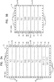
- Fig. 3B is a diagram that schematically illustrates the structure of RFIC 34, which is configured to operate at a 2.4GHz frequency, in accordance with an embodiment of the present invention.
- RFIC 34 comprises seven (7) modules of transmit/receive chains TX/RX0 - TX/RX2. Each module represents a transmit chain, or a receive chain, or a frequency source of the chains.
- the on-chip location of corresponding chains and frequency sources (in this case, the TX/RX0 - TX/RX2 chains and the SX0 DFS frequency source), and their respective bond pads 54 and 56, are identical for RFICs 32 and 34.
- the modules [TX1,RX1,SX0,TX0,RX0,TX2,RX2] are arranged in the same order on RFIC 32 and on RFIC 34.
- This design commonality enables interchangeability between RFICs 32 and 34 and their respective MCMs 28 and 30.
- MCMs 28 and 30 can use an identical BBIC 36, as shown in Fig. 1 .
- both RFIC 32 and RFIC 34 can be bonded to BBIC 36 using direct bond wires that do not cross over one another.
- using a common structure and interface of the TX/RX chains at the RFICs allows formation of multiple-band devices using the same BBIC and similar wiring and packaging schemes in the corresponding MCMs.
- RFIC 32 comprises 11 modules
- RFIC 34 comprises 7 modules.
- RFIC 32 there is a different number of transceiver chains in RFIC 32 compared to RFIC 34.
- the common transceiver chains in both RFICs are lined up identically facing their corresponding circuitry in the BBIC.
- RFICs 32 and 34 are interchangeable with each other in relation to the interface with BBIC.
- bond pads 54 and 56 of the RFICs and the BBIC are configured to avoid crossing wires between the RFIC and the BBIC, in case of switching RFIC 32 with RFIC 34, and vice versa.
- RFIC 32 comprises a basic configuration set of transceiver chains (e.g., TX/RX 0 - TX/RX 2), which is identical to the configuration of the same set of transceiver chain of RFIC 34.
- RFIC 32 comprises one or more additional transceiver sets (or sections), such as TX/RX 3 and/or the RX auxiliary chain, as shown in Fig. 1 .
- the additional transceiver sets (sections) are laid on one or more edges of a contiguous block comprising the basic configuration set of transceiver chains (denoted TX/RX 0 - TX/RX 2).
- the layout of the various chains in the RFIC floor plans are not restricted to the configuration illustrated in Figs. 3A and 3B .
- the important feature is that the interfaces between the RFIC and the BBIC (pads 56) should be configured at the RFICs and the BBICs as described in Figs. 3A and 3B , to avoid crossing wires between the RFIC and the BBIC.
- the pads configuration in RFIC 34 are a subset of the pads in RFIC 32.
- both RFICs comprise three TX/RX chains (TX/RX 0 - TX/RX 2), and their respective pads are at identical locations in the RFIC.
- RFIC 32 comprises additional groups of pads and the DFS groups, which are not present in RFIC 34.
- Figs. 3A-3B The configuration presented in Figs. 3A-3B is an example. In alternative embodiments, any other suitable configuration may be used for the same frequency bands as well as for different frequencies.
Landscapes
- Engineering & Computer Science (AREA)
- Computer Networks & Wireless Communication (AREA)
- Signal Processing (AREA)
- Transceivers (AREA)
Claims (6)
- Vorrichtung für drahtlose lokale Netzwerke (WLAN) (20), umfassend:einen ersten Sende-Empfänger (28), der ausgelegt ist, auf einem ersten Frequenzband zu kommunizieren, und der ein erstes Mehrchipmodul (MCM) umfasst, das einen ersten integrierten Funkfrequenzschaltkreis (RFIC) (32) zum Senden und Empfangen auf dem ersten Frequenzband und einen ersten integrierten Basisbandschaltkreis (BBIC) umfasst; undeinen zweiten Sende-Empfänger (30), der ausgelegt ist, auf einem zweiten Frequenzband zu kommunizieren, und der ein zweites MCM umfasst, das einen zweiten RFIC (34) zum Senden und Empfangen auf dem zweiten Frequenzband und einen zweiten BBIC umfasst, der mit dem ersten BBIC identisch ist,wobei der erste und der zweite RFIC und der erste und der zweite BBIC (36) Bondinseln (54, 56) umfassen, um Schnittstellen bereitzustellen, wobei der erste RFIC mit dem ersten BBIC verbunden ist und der zweite RFIC mit dem zweiten BBIC verbunden ist, unter Verwendung von direkten Bonddrähten zwischen den Bondinseln (54, 56), und wobei die Bondinseln jedes des ersten und des zweiten RFICs und des ersten und des zweiten BBICs so positioniert sind, dass keine zwei der direkten Bonddrähte übereinander kreuzen,wobei der erste RFIC einen grundlegenden Konfigurationssatz von Sende-Empfänger-Ketten umfasst und wobei der zweite RFIC einen grundlegenden Konfigurationssatz von Sende-Empfänger-Ketten umfasst, der jeweils dem grundlegenden Konfigurationssatz von Sende-Empfänger-Ketten des ersten RFIC sowie einer oder mehreren zusätzlichen Sende-Empfänger-Ketten entspricht,und wobei die Schnittstellen der Sende-Empfänger-Ketten im zweiten RFIC in der gleichen Reihenfolge wie entsprechende Schnittstellen der Sende-Empfänger-Ketten im ersten RFIC gereiht sind, und wobei die eine oder die mehreren zusätzlichen Sende-Empfänger-Ketten des zweiten RFIC an einer oder mehreren Kanten eines zusammenhängenden Blocks verlegt sind, der den grundlegenden Konfigurationssatz der Sende-Empfänger-Ketten bildet.
- WLAN-Vorrichtung nach Anspruch 1, wobei die Schnittstellen der Sende-Empfänger-Ketten im ersten und zweiten RFIC ausgelegt sind, jeweiligen Basisbandschaltkreisen im ersten bzw. zweiten BBIC gegenüberzuliegen.
- Verfahren, umfassend:durch eine drahtlose lokale Netzwerk-Vorrichtung (WLAN-Vorrichtung), die auf einem ersten Frequenzband unter Verwendung eines ersten Mehrchipmoduls (MCM) kommuniziert,das einen ersten integrierten Funkfrequenzschaltkreis (RFIC) (32) zum Senden und Empfangen auf dem ersten Frequenzband und einen ersten integrierten Basisbandschaltkreis (BBIC) umfasst; undgleichzeitig auf einem zweiten Frequenzband unter Verwendung eines zweiten MCM kommuniziert, das einen zweiten RFIC (34) zum Senden und Empfangen auf dem zweiten Frequenzband undeinen zweiten BBIC umfasst, der mit dem ersten BBIC identisch ist,wobei der erste und der zweite RFIC und der erste und der zweite BBIC (36) Bondinseln umfassen, um Schnittstellen bereitzustellen, wobei der erste RFIC mit dem ersten BBIC verbunden ist und der zweite RFIC mit dem zweiten BBIC verbunden ist, unter Verwendung von direkten Bonddrähten zwischen den Bondinseln (54, 56), und wobei die Bondinseln jedes des ersten und des zweiten RFICs und des ersten und des zweiten BBICs so positioniert sind, dass keine zwei der direkten Bonddrähte übereinander kreuzen,wobei der erste RFIC einen grundlegenden Konfigurationssatz von Sende-Empfänger-Ketten umfasst und wobei der zweite RFIC einen grundlegenden Konfigurationssatz von Sende-Empfänger-Ketten umfasst, der jeweils dem grundlegenden Konfigurationssatz von Sende-Empfänger-Ketten des ersten RFIC sowie einer oder mehreren zusätzlichen Sende-Empfänger-Ketten entspricht,und wobei die Schnittstellen der Sende-Empfänger-Ketten im zweiten RFIC in der gleichen Reihenfolge wie entsprechende Schnittstellen der ersten Sende-Empfänger-Ketten im ersten RFIC gereiht sind, und wobei die zusätzlichen Sende-Empfänger-Ketten an einer oder mehreren Kanten eines zusammenhängenden Blocks verlegt sind, der den grundlegenden Konfigurationssatz der Sende-Empfänger-Ketten bildet.
- Verfahren nach Anspruch 3, wobei die Schnittstellen der Sende-Empfänger-Ketten im ersten und zweiten RFICs ausgelegt sind, jeweiligen Basisbandschaltkreisen im ersten bzw. zweiten BBIC gegenüberzuliegen.
- Verfahren, umfassend:Erzeugen eines ersten Sende-Empfängers, der ein erstes Mehrchipmodul (MCM) umfasst, das einen ersten integrierten Funkfrequenzschaltkreis (RFIC) zum Senden und Empfangen auf einem ersten Frequenzband und einen ersten integrierten Basisbandschaltkreis (BBIC) umfasst;Erzeugen eines zweiten Sende-Empfängers, der ein zweites MCM umfasst, das einen zweiten RFIC zum Senden und Empfangen auf einem zweiten Frequenzband und einen zweiten BBIC umfasst, der mit dem ersten BBIC identisch ist; undIntegrieren des ersten und des zweiten Sende-Empfängers, um eine gleichzeitige Zweiband-Kommunikationsvorrichtung zu erzeugen,wobei der erste und der zweite RFIC und der erste und der zweite BBIC Bondinseln umfassen, um Schnittstellen bereitzustellen, um den ersten RFIC mit dem ersten BBIC zu verbinden und den zweiten RFIC mit dem zweiten BBIC zu verbinden, unter Verwendung von direkten Bonddrähten zwischen den Bondinseln, wobei die Bondinseln jedes des ersten und des zweiten RFICs und des ersten und des zweiten BBICs so positioniert sind, dass keine zwei der direkten Bonddrähte übereinander kreuzen,wobei der erste RFIC einen grundlegenden Konfigurationssatz von Sende-Empfänger-Ketten umfasst und wobei der zweite RFIC einen grundlegenden Konfigurationssatz von Sende-Empfänger-Ketten umfasst, der jeweils dem grundlegenden Konfigurationssatz von Sende-Empfänger-Ketten des ersten RFIC sowie einer oder mehreren zusätzlichen Sende-Empfänger-Ketten entspricht,und wobei die Sende-Empfänger-Ketten im zweiten RFIC nebeneinander in einem zusammenhängenden Block verlegt und in der gleichen Reihenfolge wie der grundlegende Konfigurationssatz der Sende-Empfänger-Ketten im ersten RFIC gereiht sind, und wobei die zusätzlichen Sende-Empfänger-Ketten an einer oder mehreren Kanten des zusammenhängenden Blocks verlegt sind.
- Verfahren nach Anspruch 5, wobei die Schnittstellen der Sende-Empfänger-Ketten im ersten und zweiten RFICs ausgelegt sind, jeweiligen Basisbandschaltkreisen im ersten bzw. zweiten BBIC gegenüberzuliegen.
Applications Claiming Priority (1)
| Application Number | Priority Date | Filing Date | Title |
|---|---|---|---|
| PCT/IB2014/063473 WO2016016684A1 (en) | 2014-07-28 | 2014-07-28 | Concurrent dual-band wlan device using mcm |
Publications (3)
| Publication Number | Publication Date |
|---|---|
| EP3175674A1 EP3175674A1 (de) | 2017-06-07 |
| EP3175674A4 EP3175674A4 (de) | 2018-03-28 |
| EP3175674B1 true EP3175674B1 (de) | 2019-07-03 |
Family
ID=55216812
Family Applications (1)
| Application Number | Title | Priority Date | Filing Date |
|---|---|---|---|
| EP14898565.8A Active EP3175674B1 (de) | 2014-07-28 | 2014-07-28 | Gleichzeitige dualband-wlan-vorrichtung mit mcm |
Country Status (3)
| Country | Link |
|---|---|
| EP (1) | EP3175674B1 (de) |
| CN (1) | CN106664105A (de) |
| WO (1) | WO2016016684A1 (de) |
Families Citing this family (1)
| Publication number | Priority date | Publication date | Assignee | Title |
|---|---|---|---|---|
| US10523249B2 (en) * | 2017-09-20 | 2019-12-31 | Frontiir PTE Ltd | Directional dual-radio wireless repeater |
Family Cites Families (8)
| Publication number | Priority date | Publication date | Assignee | Title |
|---|---|---|---|---|
| US6047175A (en) * | 1996-06-28 | 2000-04-04 | Aironet Wireless Communications, Inc. | Wireless communication method and device with auxiliary receiver for selecting different channels |
| CN100544217C (zh) * | 2005-04-04 | 2009-09-23 | 美国博通公司 | 射频收发器集成电路及其本振电路 |
| US8139670B1 (en) * | 2007-09-21 | 2012-03-20 | Marvell International Ltd. | Modular MIMO transceiver architecture |
| US8594050B2 (en) * | 2007-12-28 | 2013-11-26 | Intel Corporation | Techniques to control wireless personal area networks |
| JP5316305B2 (ja) * | 2009-08-13 | 2013-10-16 | ソニー株式会社 | 無線伝送システム、無線伝送方法 |
| US9031048B2 (en) * | 2011-03-30 | 2015-05-12 | Broadcom Corporation | Dual band wireless local area network (WLAN) transceiver |
| KR20130134193A (ko) * | 2012-05-30 | 2013-12-10 | 삼성전자주식회사 | 컨커런트 서비스를 제공하기 위한 전자 장치 및 방법 |
| US20140131854A1 (en) * | 2012-11-13 | 2014-05-15 | Lsi Corporation | Multi-chip module connection by way of bridging blocks |
-
2014
- 2014-07-28 WO PCT/IB2014/063473 patent/WO2016016684A1/en not_active Ceased
- 2014-07-28 EP EP14898565.8A patent/EP3175674B1/de active Active
- 2014-07-28 CN CN201480080651.4A patent/CN106664105A/zh active Pending
Non-Patent Citations (1)
| Title |
|---|
| None * |
Also Published As
| Publication number | Publication date |
|---|---|
| WO2016016684A1 (en) | 2016-02-04 |
| EP3175674A4 (de) | 2018-03-28 |
| EP3175674A1 (de) | 2017-06-07 |
| CN106664105A (zh) | 2017-05-10 |
Similar Documents
| Publication | Publication Date | Title |
|---|---|---|
| US9467195B2 (en) | Concurrent dual-band WLAN device using MCM | |
| US12040541B2 (en) | Radio frequency systems with tunable filter | |
| US9288031B2 (en) | Switch arrangement | |
| KR102652348B1 (ko) | 고조파의 빔형성 | |
| EP3847849B1 (de) | Dynamisch konfigurierbare drahtlose vorrichtung mit mehreren gleichzeitigen frequenzbändern | |
| TWI526005B (zh) | 無線通訊終端機 | |
| CN102185623B (zh) | 一种移动终端及其多天线实现方法 | |
| EP4220971A1 (de) | Hochfrequenz-drx-vorrichtung, hochfrequenzsystem und kommunikationsvorrichtung | |
| US8948707B2 (en) | Duplex filter arrangements for use with tunable narrow band antennas having forward and backward compatibility | |
| US8290536B2 (en) | Radio transceiver and method for reception of combined receive signals | |
| US9413444B2 (en) | Radio-frequency processing circuit and related wireless communication device | |
| EP4254812B1 (de) | Funkfrequenzsendeempfangssystem und kommunikationsvorrichtung | |
| EP4254814A1 (de) | Hochfrequenz-pa-mid-vorrichtung, hochfrequenz-sendeempfangssystem und kommunikationsvorrichtung | |
| CN110504984A (zh) | 一种电子设备 | |
| US7162266B2 (en) | Multiple band handset architecture | |
| EP4258562A1 (de) | Funkfrequenzsendeempfangssystem und kommunikationsvorrichtung | |
| WO2022193842A1 (zh) | 晶粒的制造方法 | |
| EP3175674A1 (de) | Gleichzeitige dualband-wlan-vorrichtung mit mcm | |
| EP4329203A1 (de) | Verfahren und vorrichtungen zur gemeinsamen antennennutzung unter verwendung eines funkkopfes in einem verteilten funksystem | |
| EP4258556B1 (de) | Funkfrequenzsendeempfänger und kommunikationsvorrichtung | |
| JP4865870B2 (ja) | アンテナシステムにおける受信信号を導く装置及び方法 | |
| CN113726361B (zh) | 射频l-drx器件、射频收发系统和通信设备 | |
| TWI916686B (zh) | 具有可調濾波器之射頻系統 | |
| KR20250083365A (ko) | 튜닝가능 필터 배열 | |
| WO2023048613A1 (en) | An electronic device, a method, a computer program product, and a single-chip radio |
Legal Events
| Date | Code | Title | Description |
|---|---|---|---|
| STAA | Information on the status of an ep patent application or granted ep patent |
Free format text: STATUS: THE INTERNATIONAL PUBLICATION HAS BEEN MADE |
|
| 17P | Request for examination filed |
Effective date: 20161229 |
|
| AK | Designated contracting states |
Kind code of ref document: A1 Designated state(s): AL AT BE BG CH CY CZ DE DK EE ES FI FR GB GR HR HU IE IS IT LI LT LU LV MC MK MT NL NO PL PT RO RS SE SI SK SM TR |
|
| AX | Request for extension of the european patent |
Extension state: BA ME |
|
| PUAI | Public reference made under article 153(3) epc to a published international application that has entered the european phase |
Free format text: ORIGINAL CODE: 0009012 |
|
| STAA | Information on the status of an ep patent application or granted ep patent |
Free format text: STATUS: REQUEST FOR EXAMINATION WAS MADE |
|
| DAX | Request for extension of the european patent (deleted) | ||
| A4 | Supplementary search report drawn up and despatched |
Effective date: 20180228 |
|
| RIC1 | Information provided on ipc code assigned before grant |
Ipc: H04B 1/38 20150101AFI20180222BHEP Ipc: H01L 23/48 20060101ALN20180222BHEP Ipc: H01L 21/02 20060101ALI20180222BHEP Ipc: H01L 25/065 20060101ALI20180222BHEP |
|
| REG | Reference to a national code |
Ref country code: DE Ref legal event code: R079 Ref document number: 602014049701 Country of ref document: DE Free format text: PREVIOUS MAIN CLASS: H04W0088060000 Ipc: H04B0001380000 |
|
| GRAP | Despatch of communication of intention to grant a patent |
Free format text: ORIGINAL CODE: EPIDOSNIGR1 |
|
| STAA | Information on the status of an ep patent application or granted ep patent |
Free format text: STATUS: GRANT OF PATENT IS INTENDED |
|
| RIC1 | Information provided on ipc code assigned before grant |
Ipc: H04B 1/38 20150101AFI20190121BHEP Ipc: H01L 25/065 20060101ALI20190121BHEP |
|
| INTG | Intention to grant announced |
Effective date: 20190212 |
|
| GRAS | Grant fee paid |
Free format text: ORIGINAL CODE: EPIDOSNIGR3 |
|
| GRAA | (expected) grant |
Free format text: ORIGINAL CODE: 0009210 |
|
| STAA | Information on the status of an ep patent application or granted ep patent |
Free format text: STATUS: THE PATENT HAS BEEN GRANTED |
|
| AK | Designated contracting states |
Kind code of ref document: B1 Designated state(s): AL AT BE BG CH CY CZ DE DK EE ES FI FR GB GR HR HU IE IS IT LI LT LU LV MC MK MT NL NO PL PT RO RS SE SI SK SM TR |
|
| REG | Reference to a national code |
Ref country code: GB Ref legal event code: FG4D |
|
| REG | Reference to a national code |
Ref country code: CH Ref legal event code: EP Ref country code: AT Ref legal event code: REF Ref document number: 1152230 Country of ref document: AT Kind code of ref document: T Effective date: 20190715 |
|
| REG | Reference to a national code |
Ref country code: IE Ref legal event code: FG4D |
|
| REG | Reference to a national code |
Ref country code: DE Ref legal event code: R096 Ref document number: 602014049701 Country of ref document: DE |
|
| REG | Reference to a national code |
Ref country code: NL Ref legal event code: MP Effective date: 20190703 |
|
| REG | Reference to a national code |
Ref country code: LT Ref legal event code: MG4D |
|
| REG | Reference to a national code |
Ref country code: AT Ref legal event code: MK05 Ref document number: 1152230 Country of ref document: AT Kind code of ref document: T Effective date: 20190703 |
|
| PG25 | Lapsed in a contracting state [announced via postgrant information from national office to epo] |
Ref country code: FI Free format text: LAPSE BECAUSE OF FAILURE TO SUBMIT A TRANSLATION OF THE DESCRIPTION OR TO PAY THE FEE WITHIN THE PRESCRIBED TIME-LIMIT Effective date: 20190703 Ref country code: LT Free format text: LAPSE BECAUSE OF FAILURE TO SUBMIT A TRANSLATION OF THE DESCRIPTION OR TO PAY THE FEE WITHIN THE PRESCRIBED TIME-LIMIT Effective date: 20190703 Ref country code: NL Free format text: LAPSE BECAUSE OF FAILURE TO SUBMIT A TRANSLATION OF THE DESCRIPTION OR TO PAY THE FEE WITHIN THE PRESCRIBED TIME-LIMIT Effective date: 20190703 Ref country code: CZ Free format text: LAPSE BECAUSE OF FAILURE TO SUBMIT A TRANSLATION OF THE DESCRIPTION OR TO PAY THE FEE WITHIN THE PRESCRIBED TIME-LIMIT Effective date: 20190703 Ref country code: PT Free format text: LAPSE BECAUSE OF FAILURE TO SUBMIT A TRANSLATION OF THE DESCRIPTION OR TO PAY THE FEE WITHIN THE PRESCRIBED TIME-LIMIT Effective date: 20191104 Ref country code: BG Free format text: LAPSE BECAUSE OF FAILURE TO SUBMIT A TRANSLATION OF THE DESCRIPTION OR TO PAY THE FEE WITHIN THE PRESCRIBED TIME-LIMIT Effective date: 20191003 Ref country code: NO Free format text: LAPSE BECAUSE OF FAILURE TO SUBMIT A TRANSLATION OF THE DESCRIPTION OR TO PAY THE FEE WITHIN THE PRESCRIBED TIME-LIMIT Effective date: 20191003 Ref country code: AT Free format text: LAPSE BECAUSE OF FAILURE TO SUBMIT A TRANSLATION OF THE DESCRIPTION OR TO PAY THE FEE WITHIN THE PRESCRIBED TIME-LIMIT Effective date: 20190703 Ref country code: HR Free format text: LAPSE BECAUSE OF FAILURE TO SUBMIT A TRANSLATION OF THE DESCRIPTION OR TO PAY THE FEE WITHIN THE PRESCRIBED TIME-LIMIT Effective date: 20190703 Ref country code: SE Free format text: LAPSE BECAUSE OF FAILURE TO SUBMIT A TRANSLATION OF THE DESCRIPTION OR TO PAY THE FEE WITHIN THE PRESCRIBED TIME-LIMIT Effective date: 20190703 |
|
| PG25 | Lapsed in a contracting state [announced via postgrant information from national office to epo] |
Ref country code: IS Free format text: LAPSE BECAUSE OF FAILURE TO SUBMIT A TRANSLATION OF THE DESCRIPTION OR TO PAY THE FEE WITHIN THE PRESCRIBED TIME-LIMIT Effective date: 20191103 Ref country code: RS Free format text: LAPSE BECAUSE OF FAILURE TO SUBMIT A TRANSLATION OF THE DESCRIPTION OR TO PAY THE FEE WITHIN THE PRESCRIBED TIME-LIMIT Effective date: 20190703 Ref country code: ES Free format text: LAPSE BECAUSE OF FAILURE TO SUBMIT A TRANSLATION OF THE DESCRIPTION OR TO PAY THE FEE WITHIN THE PRESCRIBED TIME-LIMIT Effective date: 20190703 Ref country code: GR Free format text: LAPSE BECAUSE OF FAILURE TO SUBMIT A TRANSLATION OF THE DESCRIPTION OR TO PAY THE FEE WITHIN THE PRESCRIBED TIME-LIMIT Effective date: 20191004 Ref country code: LV Free format text: LAPSE BECAUSE OF FAILURE TO SUBMIT A TRANSLATION OF THE DESCRIPTION OR TO PAY THE FEE WITHIN THE PRESCRIBED TIME-LIMIT Effective date: 20190703 Ref country code: AL Free format text: LAPSE BECAUSE OF FAILURE TO SUBMIT A TRANSLATION OF THE DESCRIPTION OR TO PAY THE FEE WITHIN THE PRESCRIBED TIME-LIMIT Effective date: 20190703 |
|
| REG | Reference to a national code |
Ref country code: CH Ref legal event code: PL |
|
| PG25 | Lapsed in a contracting state [announced via postgrant information from national office to epo] |
Ref country code: TR Free format text: LAPSE BECAUSE OF FAILURE TO SUBMIT A TRANSLATION OF THE DESCRIPTION OR TO PAY THE FEE WITHIN THE PRESCRIBED TIME-LIMIT Effective date: 20190703 |
|
| PG25 | Lapsed in a contracting state [announced via postgrant information from national office to epo] |
Ref country code: EE Free format text: LAPSE BECAUSE OF FAILURE TO SUBMIT A TRANSLATION OF THE DESCRIPTION OR TO PAY THE FEE WITHIN THE PRESCRIBED TIME-LIMIT Effective date: 20190703 Ref country code: IT Free format text: LAPSE BECAUSE OF FAILURE TO SUBMIT A TRANSLATION OF THE DESCRIPTION OR TO PAY THE FEE WITHIN THE PRESCRIBED TIME-LIMIT Effective date: 20190703 Ref country code: DK Free format text: LAPSE BECAUSE OF FAILURE TO SUBMIT A TRANSLATION OF THE DESCRIPTION OR TO PAY THE FEE WITHIN THE PRESCRIBED TIME-LIMIT Effective date: 20190703 Ref country code: RO Free format text: LAPSE BECAUSE OF FAILURE TO SUBMIT A TRANSLATION OF THE DESCRIPTION OR TO PAY THE FEE WITHIN THE PRESCRIBED TIME-LIMIT Effective date: 20190703 Ref country code: PL Free format text: LAPSE BECAUSE OF FAILURE TO SUBMIT A TRANSLATION OF THE DESCRIPTION OR TO PAY THE FEE WITHIN THE PRESCRIBED TIME-LIMIT Effective date: 20190703 |
|
| PG25 | Lapsed in a contracting state [announced via postgrant information from national office to epo] |
Ref country code: SK Free format text: LAPSE BECAUSE OF FAILURE TO SUBMIT A TRANSLATION OF THE DESCRIPTION OR TO PAY THE FEE WITHIN THE PRESCRIBED TIME-LIMIT Effective date: 20190703 Ref country code: CH Free format text: LAPSE BECAUSE OF NON-PAYMENT OF DUE FEES Effective date: 20190731 Ref country code: LI Free format text: LAPSE BECAUSE OF NON-PAYMENT OF DUE FEES Effective date: 20190731 Ref country code: MC Free format text: LAPSE BECAUSE OF FAILURE TO SUBMIT A TRANSLATION OF THE DESCRIPTION OR TO PAY THE FEE WITHIN THE PRESCRIBED TIME-LIMIT Effective date: 20190703 Ref country code: LU Free format text: LAPSE BECAUSE OF NON-PAYMENT OF DUE FEES Effective date: 20190728 Ref country code: IS Free format text: LAPSE BECAUSE OF FAILURE TO SUBMIT A TRANSLATION OF THE DESCRIPTION OR TO PAY THE FEE WITHIN THE PRESCRIBED TIME-LIMIT Effective date: 20200224 Ref country code: SM Free format text: LAPSE BECAUSE OF FAILURE TO SUBMIT A TRANSLATION OF THE DESCRIPTION OR TO PAY THE FEE WITHIN THE PRESCRIBED TIME-LIMIT Effective date: 20190703 |
|
| REG | Reference to a national code |
Ref country code: DE Ref legal event code: R097 Ref document number: 602014049701 Country of ref document: DE |
|
| PLBE | No opposition filed within time limit |
Free format text: ORIGINAL CODE: 0009261 |
|
| STAA | Information on the status of an ep patent application or granted ep patent |
Free format text: STATUS: NO OPPOSITION FILED WITHIN TIME LIMIT |
|
| PG2D | Information on lapse in contracting state deleted |
Ref country code: IS |
|
| PG25 | Lapsed in a contracting state [announced via postgrant information from national office to epo] |
Ref country code: IE Free format text: LAPSE BECAUSE OF NON-PAYMENT OF DUE FEES Effective date: 20190728 |
|
| 26N | No opposition filed |
Effective date: 20200603 |
|
| PG25 | Lapsed in a contracting state [announced via postgrant information from national office to epo] |
Ref country code: SI Free format text: LAPSE BECAUSE OF FAILURE TO SUBMIT A TRANSLATION OF THE DESCRIPTION OR TO PAY THE FEE WITHIN THE PRESCRIBED TIME-LIMIT Effective date: 20190703 |
|
| PG25 | Lapsed in a contracting state [announced via postgrant information from national office to epo] |
Ref country code: CY Free format text: LAPSE BECAUSE OF FAILURE TO SUBMIT A TRANSLATION OF THE DESCRIPTION OR TO PAY THE FEE WITHIN THE PRESCRIBED TIME-LIMIT Effective date: 20190703 |
|
| PG25 | Lapsed in a contracting state [announced via postgrant information from national office to epo] |
Ref country code: MT Free format text: LAPSE BECAUSE OF FAILURE TO SUBMIT A TRANSLATION OF THE DESCRIPTION OR TO PAY THE FEE WITHIN THE PRESCRIBED TIME-LIMIT Effective date: 20190703 Ref country code: HU Free format text: LAPSE BECAUSE OF FAILURE TO SUBMIT A TRANSLATION OF THE DESCRIPTION OR TO PAY THE FEE WITHIN THE PRESCRIBED TIME-LIMIT; INVALID AB INITIO Effective date: 20140728 |
|
| PG25 | Lapsed in a contracting state [announced via postgrant information from national office to epo] |
Ref country code: MK Free format text: LAPSE BECAUSE OF FAILURE TO SUBMIT A TRANSLATION OF THE DESCRIPTION OR TO PAY THE FEE WITHIN THE PRESCRIBED TIME-LIMIT Effective date: 20190703 |
|
| PGFP | Annual fee paid to national office [announced via postgrant information from national office to epo] |
Ref country code: BE Payment date: 20240719 Year of fee payment: 11 |
|
| PGFP | Annual fee paid to national office [announced via postgrant information from national office to epo] |
Ref country code: FR Payment date: 20240730 Year of fee payment: 11 |
|
| P01 | Opt-out of the competence of the unified patent court (upc) registered |
Free format text: CASE NUMBER: UPC_APP_327007/2023 Effective date: 20230524 |
|
| PGFP | Annual fee paid to national office [announced via postgrant information from national office to epo] |
Ref country code: DE Payment date: 20250722 Year of fee payment: 12 |
|
| PGFP | Annual fee paid to national office [announced via postgrant information from national office to epo] |
Ref country code: GB Payment date: 20250722 Year of fee payment: 12 |
|
| REG | Reference to a national code |
Ref country code: BE Ref legal event code: MM Effective date: 20250731 |
|
| PG25 | Lapsed in a contracting state [announced via postgrant information from national office to epo] |
Ref country code: BE Free format text: LAPSE BECAUSE OF NON-PAYMENT OF DUE FEES Effective date: 20250731 |
|
| PG25 | Lapsed in a contracting state [announced via postgrant information from national office to epo] |
Ref country code: FR Free format text: LAPSE BECAUSE OF NON-PAYMENT OF DUE FEES Effective date: 20250731 |