EP3174102A1 - Semiconductor device and method of making a semiconductor device - Google Patents
Semiconductor device and method of making a semiconductor device Download PDFInfo
- Publication number
- EP3174102A1 EP3174102A1 EP15196730.4A EP15196730A EP3174102A1 EP 3174102 A1 EP3174102 A1 EP 3174102A1 EP 15196730 A EP15196730 A EP 15196730A EP 3174102 A1 EP3174102 A1 EP 3174102A1
- Authority
- EP
- European Patent Office
- Prior art keywords
- electrically conductive
- conductive material
- trench
- layer
- contact
- Prior art date
- Legal status (The legal status is an assumption and is not a legal conclusion. Google has not performed a legal analysis and makes no representation as to the accuracy of the status listed.)
- Granted
Links
Images



Classifications
-
- H—ELECTRICITY
- H10—SEMICONDUCTOR DEVICES; ELECTRIC SOLID-STATE DEVICES NOT OTHERWISE PROVIDED FOR
- H10D—INORGANIC ELECTRIC SEMICONDUCTOR DEVICES
- H10D30/00—Field-effect transistors [FET]
- H10D30/40—FETs having zero-dimensional [0D], one-dimensional [1D] or two-dimensional [2D] charge carrier gas channels
- H10D30/47—FETs having zero-dimensional [0D], one-dimensional [1D] or two-dimensional [2D] charge carrier gas channels having two-dimensional [2D] charge carrier gas channels, e.g. nanoribbon FETs or high electron mobility transistors [HEMT]
- H10D30/471—High electron mobility transistors [HEMT] or high hole mobility transistors [HHMT]
- H10D30/475—High electron mobility transistors [HEMT] or high hole mobility transistors [HHMT] having wider bandgap layer formed on top of lower bandgap active layer, e.g. undoped barrier HEMTs such as i-AlGaN/GaN HEMTs
- H10D30/4755—High electron mobility transistors [HEMT] or high hole mobility transistors [HHMT] having wider bandgap layer formed on top of lower bandgap active layer, e.g. undoped barrier HEMTs such as i-AlGaN/GaN HEMTs having wide bandgap charge-carrier supplying layers, e.g. modulation doped HEMTs such as n-AlGaAs/GaAs HEMTs
-
- H—ELECTRICITY
- H10—SEMICONDUCTOR DEVICES; ELECTRIC SOLID-STATE DEVICES NOT OTHERWISE PROVIDED FOR
- H10D—INORGANIC ELECTRIC SEMICONDUCTOR DEVICES
- H10D30/00—Field-effect transistors [FET]
- H10D30/01—Manufacture or treatment
- H10D30/015—Manufacture or treatment of FETs having heterojunction interface channels or heterojunction gate electrodes, e.g. HEMT
-
- H—ELECTRICITY
- H10—SEMICONDUCTOR DEVICES; ELECTRIC SOLID-STATE DEVICES NOT OTHERWISE PROVIDED FOR
- H10D—INORGANIC ELECTRIC SEMICONDUCTOR DEVICES
- H10D30/00—Field-effect transistors [FET]
- H10D30/40—FETs having zero-dimensional [0D], one-dimensional [1D] or two-dimensional [2D] charge carrier gas channels
- H10D30/47—FETs having zero-dimensional [0D], one-dimensional [1D] or two-dimensional [2D] charge carrier gas channels having two-dimensional [2D] charge carrier gas channels, e.g. nanoribbon FETs or high electron mobility transistors [HEMT]
- H10D30/471—High electron mobility transistors [HEMT] or high hole mobility transistors [HHMT]
- H10D30/475—High electron mobility transistors [HEMT] or high hole mobility transistors [HHMT] having wider bandgap layer formed on top of lower bandgap active layer, e.g. undoped barrier HEMTs such as i-AlGaN/GaN HEMTs
-
- H—ELECTRICITY
- H10—SEMICONDUCTOR DEVICES; ELECTRIC SOLID-STATE DEVICES NOT OTHERWISE PROVIDED FOR
- H10D—INORGANIC ELECTRIC SEMICONDUCTOR DEVICES
- H10D62/00—Semiconductor bodies, or regions thereof, of devices having potential barriers
- H10D62/80—Semiconductor bodies, or regions thereof, of devices having potential barriers characterised by the materials
- H10D62/85—Semiconductor bodies, or regions thereof, of devices having potential barriers characterised by the materials being Group III-V materials, e.g. GaAs
-
- H—ELECTRICITY
- H10—SEMICONDUCTOR DEVICES; ELECTRIC SOLID-STATE DEVICES NOT OTHERWISE PROVIDED FOR
- H10D—INORGANIC ELECTRIC SEMICONDUCTOR DEVICES
- H10D62/00—Semiconductor bodies, or regions thereof, of devices having potential barriers
- H10D62/80—Semiconductor bodies, or regions thereof, of devices having potential barriers characterised by the materials
- H10D62/85—Semiconductor bodies, or regions thereof, of devices having potential barriers characterised by the materials being Group III-V materials, e.g. GaAs
- H10D62/8503—Nitride Group III-V materials, e.g. AlN or GaN
-
- H—ELECTRICITY
- H10—SEMICONDUCTOR DEVICES; ELECTRIC SOLID-STATE DEVICES NOT OTHERWISE PROVIDED FOR
- H10D—INORGANIC ELECTRIC SEMICONDUCTOR DEVICES
- H10D64/00—Electrodes of devices having potential barriers
- H10D64/01—Manufacture or treatment
-
- H—ELECTRICITY
- H10—SEMICONDUCTOR DEVICES; ELECTRIC SOLID-STATE DEVICES NOT OTHERWISE PROVIDED FOR
- H10D—INORGANIC ELECTRIC SEMICONDUCTOR DEVICES
- H10D64/00—Electrodes of devices having potential barriers
- H10D64/20—Electrodes characterised by their shapes, relative sizes or dispositions
- H10D64/23—Electrodes carrying the current to be rectified, amplified, oscillated or switched, e.g. sources, drains, anodes or cathodes
- H10D64/251—Source or drain electrodes for field-effect devices
- H10D64/256—Source or drain electrodes for field-effect devices for lateral devices wherein the source or drain electrodes are recessed in semiconductor bodies
-
- H—ELECTRICITY
- H10—SEMICONDUCTOR DEVICES; ELECTRIC SOLID-STATE DEVICES NOT OTHERWISE PROVIDED FOR
- H10D—INORGANIC ELECTRIC SEMICONDUCTOR DEVICES
- H10D64/00—Electrodes of devices having potential barriers
- H10D64/20—Electrodes characterised by their shapes, relative sizes or dispositions
- H10D64/27—Electrodes not carrying the current to be rectified, amplified, oscillated or switched, e.g. gates
- H10D64/311—Gate electrodes for field-effect devices
- H10D64/411—Gate electrodes for field-effect devices for FETs
- H10D64/511—Gate electrodes for field-effect devices for FETs for IGFETs
- H10D64/512—Disposition of the gate electrodes, e.g. buried gates
- H10D64/513—Disposition of the gate electrodes, e.g. buried gates within recesses in the substrate, e.g. trench gates, groove gates or buried gates
-
- H—ELECTRICITY
- H10—SEMICONDUCTOR DEVICES; ELECTRIC SOLID-STATE DEVICES NOT OTHERWISE PROVIDED FOR
- H10D—INORGANIC ELECTRIC SEMICONDUCTOR DEVICES
- H10D64/00—Electrodes of devices having potential barriers
- H10D64/60—Electrodes characterised by their materials
- H10D64/62—Electrodes ohmically coupled to a semiconductor
-
- H—ELECTRICITY
- H10—SEMICONDUCTOR DEVICES; ELECTRIC SOLID-STATE DEVICES NOT OTHERWISE PROVIDED FOR
- H10D—INORGANIC ELECTRIC SEMICONDUCTOR DEVICES
- H10D8/00—Diodes
- H10D8/60—Schottky-barrier diodes
-
- H—ELECTRICITY
- H10—SEMICONDUCTOR DEVICES; ELECTRIC SOLID-STATE DEVICES NOT OTHERWISE PROVIDED FOR
- H10D—INORGANIC ELECTRIC SEMICONDUCTOR DEVICES
- H10D64/00—Electrodes of devices having potential barriers
- H10D64/111—Field plates
-
- H—ELECTRICITY
- H10—SEMICONDUCTOR DEVICES; ELECTRIC SOLID-STATE DEVICES NOT OTHERWISE PROVIDED FOR
- H10D—INORGANIC ELECTRIC SEMICONDUCTOR DEVICES
- H10D64/00—Electrodes of devices having potential barriers
- H10D64/20—Electrodes characterised by their shapes, relative sizes or dispositions
- H10D64/27—Electrodes not carrying the current to be rectified, amplified, oscillated or switched, e.g. gates
Definitions
- the present specification relates to a semiconductor device and to a method of making a semiconductor device.
- HEMTs High Electron Mobility Transistors
- HV high voltage
- a GaN/AlGaN HEMT typically includes a substrate having an AlGaN layer located on a number of GaN layers.
- a gate, source and drain are located above the AlGaN layer.
- current flows between drain and source via a two-dimensional electron gas (2DEG) that is formed at the interface between the AlGaN layer and an upper GaN layer.
- 2DEG two-dimensional electron gas
- Switch-off is achieved by applying a suitable voltage to the gate, such that the 2DEG at the interface between the AlGaN layer and the uppermost GaN layer disappears.
- the gate may be a Schottky contact or may comprise a gate electrode that is isolated by a dielectric layer (such devices are referred to as Metal Insulator Semiconductor High Electron Mobility Transistors (MISHEMTs).
- MISHEMTs Metal Insulator Semiconductor High Electron Mobility Transistors
- a GaN/AlGaN Schottky diodes may be similarly constructed, but with two contacts (including a Schottky contact forming an anode and an ohmic contact forming a cathode of the device) instead of three.
- Both the HEMT and the Schottky diode suffer from the problem that the on-state resistance under dynamic (e.g. switching, pulsed, RF) conditions may be significantly higher than under DC conditions.
- dynamic e.g. switching, pulsed, RF
- a semiconductor device comprising:
- a method of making a semiconductor device comprising:
- a contact having a trench that extends down into the GaN layer of the device can provide a leakage path for holes in the GaN layer to exit the device through the contact, which may lower the on state resistance of the device under dynamic (e.g. switching, pulsed, RF) conditions.
- This leakage path can short a pn-junction formed between the two dimensional electron gas (“2DEG”) and the GaN layer.
- the first and second electrically conductive materials are different materials, and they may be chosen independently to optimise the performance of the contact of the device.
- the first electrically conductive material may be chosen to make a good ohmic contact.
- the second electrically conductive material that at least partially fills the trench may be chosen so that it forms a low resistance contact with the GaN layer.
- a material that makes a good ohmic contact may be suitable for use as the first electrically conductive material, but may not be suitable for use as the second electrically conductive material, as it may form a local n + region around the trench.
- This n + region may form a reverse biased pn junction with the p-type GaN layer located around the trench, presenting a barrier to the flow of holes.
- an electrically conductive material that is suitable for forming a low resistance path for holes may not be suitable for forming an ohmic contact portion of the device.
- the at least one contact may have a resistivity lower than approximately 1e9 ⁇ .mm. Using a typical width of the trench of 1 ⁇ m, this requirement is equivalent to a specific contact resistance lower than 10 ⁇ cm 2 .
- the at least one contact may include a central part aligned with the trench. This central part may be at least partially filled with the second electrically conductive material. The central part may be substantially surrounded by the ohmic contact portion when viewed from above the major surface.
- Such a contact may be conveniently manufactured in a manner that allows alignment of the trench relative to the ohmic contact portion (e.g. for producing a substantially symmetrical contact).
- a contact of this kind may be manufactured by initially depositing the first electrically conductive material of the ohmic contact portion, and then removing at least part of the first electrically conductive material to form an opening in the ohmic contact portion. The opening may expose a part of the major surface beneath the contact.
- the method may further include forming a trench in the part of the major surface that is exposed by the opening in the ohmic contact portion.
- the trench and the opening in the ohmic contact portion may then be at least partially filled with the second electrically conductive material.
- the second electrically conductive material take the form of a layer that lines the trench.
- the layer of the second electrically conductive material may also line the opening in the ohmic contact portion.
- a further electrically conductive material e.g. Al
- a single contiguous portion of the second electrically conductive may material form the central part and at least partially fill the trench. This may allow for an uninterrupted path for holes between the GaN layer and the top of the contact.
- the single contiguous portion may take the form of a layer as noted above, or alternatively may completely fill the trench and the central part.
- the substrate may further include a GaN cap layer located on the AlGaN layer.
- the trench of the at least one contact may pass through the GaN cap layer.
- the device may be a High Electron Mobility Transistor (HEMT) comprising a gate contact located between a source contact and a drain contact.
- the at least one of the contacts may be a drain contact of the HEMT.
- the HEMT may have a Schottky gate contact or may be a MISHEMT having an insulated gate.
- the device may be a Schottky diode and the at least one of the contacts may be a cathode of the Schottky diode.
- the gate contact of the HEMT or the anode of the Schottky diode may comprise the second electrically conductive material.
- At least one island may be located between the drain contact and the gate contact.
- Each island may include a trench extending down into the substrate from the major surface.
- the trench may pass through the AlGaN layer and into the GaN layer.
- the trench may be at least partially filled with the second electrically conductive material.
- the islands may provide additional paths for holes to exit the device. Since the trenches of the islands may be at least partially filled with the second electrically conductive material, the generation of a reverse biased pn junction of the kind described above, which may otherwise form a significant barrier to the flow of holes out of the device from the GaN layer, may be avoided.
- the islands may be connected to the drain contacts of the device.
- the islands may be formed during manufacture of the device by forming one or more trenches extending down into the substrate from the major surface, wherein each trench passes through the AlGaN layer and into the GaN layer.
- a deposition step may then be used to at least partially fill each trench with the second electrically conductive material.
- the first electrically conductive material may be an alloy of Ti/Al.
- the second electrically conductive material may be Ni, Pd, Pt or TiWN (in which the amount of N may be varied).
- Radio Frequencies are frequencies in the range 200MHz ⁇ f ⁇ 10GHz.
- the operating frequency of a device of the kind described herein may be in the range 10kHz ⁇ f ⁇ 10MHz.
- the electron mobility in a High Electron Mobility Transistor may be in the range 1000-3000 cm ⁇ 2/V/s or in the range 1000-2000 cm ⁇ 2/V/s.
- Figure 1 shows a semiconductor device 10 according to an embodiment of this disclosure.
- the device includes a substrate 2.
- the substrate 2 may, for instance, be a silicon substrate, although it is also envisaged that the substrate 2 may comprise a ceramic, glass, SiC or sapphire.
- the substrate 2 has an AlGaN layer 8 located on a GaN layer 6.
- a two dimensional electron gas or "2DEG” forms at an interface between the AlGaN layer and the GaN layer. Conduction of a current within the 2DEG forms the basis of operation of the device 10.
- buffer layers 4 comprising e.g. GaN and AlGaN may be located between the GaN layer and the underlying part of the substrate 2. These buffer layers 4 may form a super lattice acting as a stress relief region between the GaN layer 6 and the underlying part of the substrate 2.
- a GaN cap layer may be located on the AlGaN layer 8 (not shown in the Figures).
- a dielectric layer 14 may be provided on the AlGaN layer 8 (or on the GaN cap layer, if one is present). This dielectric layer may act as a passivation layer and/or may form a gate dielectric for the device 10 in the case of a MISHEMT.
- the dielectric layer 14 may, for instance, comprise SiN, SiOx or AlOx.
- the device 10 includes a plurality of contacts, one of which is shown in Figure 1 .
- the device 10 may be a High Electron Mobility Transistor (HEMT) having a source contact, a drain contact and a gate contact.
- the gate contact of the HEMT may be a Schottky contact, or alternatively may be an insulated gate (accordingly, the HEMT may be a Metal Insulator Semiconductor High Electron Mobility Transistor (MISHEMT)).
- the contact 34 shown in Figure 1 may be a drain contact of the HEMT.
- the device 10 may be a Schottky diode having an anode and a cathode.
- the contact 34 shown in Figure 1 may be a cathode of the Schottky diode, the anode of the Schottky diode being formed of a Schottky contact.
- the contact 34 shown in Figure 1 includes an ohmic contact portion 18.
- the ohmic contact portion 18 may be located on a major surface of the substrate 2.
- the ohmic contact portion 18 may be located on a surface of the AlGaN layer 8 (as is shown in Figure 1 ) or may be located on the surface of a GaN cap layer on the AlGaN layer 8, if one is present.
- the ohmic contact portion 18 may make a good ohmic contact to allow current flowing within the 2DEG at the interface between the AlGaN layer 8 and the GaN layer 6 to enter and/or exit the device 10 through the contact 34.
- the ohmic contact portion 18 comprises a first electrically conductive material that may be located on the major surface of the substrate 2.
- the contact 34 may be a recessed contact, in which the ohmic contact portion 18 extends through an opening in the AlGaN layer 8, thereby to directly contact the underlying GaN layer 6.
- a layer 22 may be located on the ohmic contact portion 18.
- the first electrically conductive material of the ohmic contact portion 18 may, for instance, comprise Ti/Al.
- the layer 22 may, for instance, comprise TiW(N).
- the layer 22 may function as a diffusion barrier during manufacture of the device 10.
- the contact 34 also includes a trench.
- the trench may extend down into the substrate 2 of the device 10 from the major surface upon which ohmic contact portion 18 is located (e.g. this may be the surface of the AlGaN layer 8 or the surface of a GaN cap layer, if one is present).
- the trench passes through the AlGaN layer 8 (and any GaN cap layer) and into the GaN layer 6. This may allow the material filling the trench (as described below) to make direct contact with the GaN layer 6, for allowing holes located in the GaN layer 6 to pass freely into the contact 34.
- the trench extends only partially into the GaN layer 6, although it is also envisaged that the trench may extend through the GaN layer 6 (e.g. to extend into the layers 4).
- the trench is at least partially filled with a second electrically conductive material 50.
- the second electrically conductive material 50 may also at least partially fill (or, as shown in Figure 1 , completely fill) a central part of the contact 34 that is substantially surrounded by the ohmic contact portion. As will be described below, the configuration and location of the central part of the contact 34 may allow for convenient manufacture of the device 10.
- a portion of the second electrically conductive material 50 may be located above the ohmic contact portion 18. For instance, in the example of Figure 1 , a portion of the electrically conductive material 50 extends over an upper surface of the layer 22.
- the trench that extends down into the GaN layer 6 of the device 10 can provide a leakage path for holes in the GaN layer 6 to exit the device 10 through the contact 34, which may lower the on state resistance of the device under dynamic (e.g. switching, pulsed, RF) conditions.
- This leakage path may short a pn-junction formed between the two dimensional electron gas ("2DEG") and the GaN layer 6.
- the second electrically conductive material 50 which at least partially fills the trench, may be chosen so that a pn-junction is not formed at an interface between the second electrically conductive material 50 and the GaN of the GaN layer 6 (e.g. at the sidewalls and/or base of the trench).
- the second electrically conductive material 50 may be chosen so as to lower the on state resistance of the device under dynamic (e.g. switching, pulsed, RF) conditions.
- the second electrically conductive material is a different electrically conductive material to the first electrically conductive material. These materials may be chosen independently, to optimise the performance of the contact 34 of the device 10.
- the first electrically conductive material, which forms the ohmic contact portion 18 may be chosen according to its suitability to make a good ohmic contact to the 2DEG.
- the second electrically conductive material 50 that at least partially fills the trench may be chosen so that it forms a low resistance contact with the GaN layer 6 (in particular, it may be chosen such that a pn junction may not form at the interface between the second electrically conductive material 50 and the GaN of the GaN layer 6, as noted above).
- a material that makes a good ohmic contact may be suitable for forming the ohmic contact portion, but may not be suitable for use as the second electrically conductive material, as it may form a local n + region in the part of the GaN layer 6 that surrounds the trench.
- This n + region may form a reverse biased pn junction with the GaN layer 6 (which is p-type).
- the pn junction may surround the trench, thereby presenting a barrier to the flow of holes, as noted previously.
- an electrically conductive material that is suitable for forming a low resistance path for holes to enter the contact 34 from the GaN layer 6 through the trench may not be suitable for forming the ohmic contact portion of the device 34.
- the first electrically conductive material which may form the ohmic contact portion 18, may comprise an alloy of Ti/Al.
- This electrically conductive material is suited to the formation of an ohmic contact.
- the second electrically conductive material 50 may comprise Ni, Pd, Pt or TiW(N).
- Figure 2 shows a semiconductor device 10 according to another embodiment of this disclosure.
- the device in Figure 2 is similar in some respects to the device 10 shown in Figure 1 , and only the differences will be described in detail here.
- the contact 34 includes a trench that is at least partially filled with a second electrically conductive material.
- the second electrically conductive material 86 is provided in the form of a layer 86 that lines the trench.
- the layer 86 may also line sidewalls of an opening in the central part of the ohmic contact portion 18.
- the layer 86 of the second electrically conductive material may, in some examples, form a diffusion barrier elsewhere in the device 10 and/or may form part of a field plate elsewhere in the device 10, as will be explained below in relation to Figure 4D .
- the second electrically conductive material comprises TiW(N), although as already noted above, other materials, such as Ni, Pd or Pt are envisaged.
- a third electrically conductive material 88 may also be provided, for filling the part of the trench and/or central part of the contact 34 that is not filled with the second electrically conductive material.
- the third electrically conductive material may, for instance, comprise Al.
- the example contact 34 in Figure 2 may also be a recessed contact as noted above in relation to Figure 1 , in which the ohmic contact portion 18 extends through an opening in the AlGaN 8 layer, thereby to directly contact the underlying GaN layer 6.
- the example in Figure 2 may also include a dielectric layer 60, the composition and purpose of which will be described below in relation to Figures 4A to 4D .
- Figures 3A to 3D show a method of making a semiconductor device according to an embodiment of this disclosure.
- the device 10 comprises a HEMT having a Schottky gate contact, although it will be appreciated that processes similar to that described here may also be used to form a MISHEMT or Schottky diode.
- the method of Figures 3A to 3D may be used to make a device 10 including at least one contact of the kind shown in, for instance, Figure 1 .
- the contact of Figure 1 forms a drain contact 34 of the device 10 to be manufactured.
- the method may include providing a substrate 2.
- the substrate 2 may be of the kind described above in relation to Figure 1 .
- the substrate 2 may, for instance, be a silicon substrate, although it is also envisaged that the substrate 2 may comprise a ceramic or glass.
- the substrate 2 has an AlGaN layer 8 located on a GaN layer 6.
- a number of buffer layers 4 comprising GaN may be located between the GaN layer and the underlying part of the substrate 2. As noted previously, these buffer layers 4 may form a super lattice that matches the lattice of the GaN layer 6 to underlying part of the substrate 2.
- a GaN cap layer may be located on the AlGaN layer 8 (not shown in the Figures).
- isolation regions 12 e.g. trenches filled with dielectric or implanted regions
- a dielectric layer 14 may be deposited on a major surface of the substrate, e.g. on a surface of the AlGaN layer 8 or any GaN cap layer that may be provided on the AlGaN layer 8. As noted previously, the dielectric layer 14 may act as a passivation layer.
- the dielectric layer 14 may comprise, for instance, SiN, SiOx or AlOx.
- openings 16 may be formed in the dielectric layer 14. These openings 16 may allow access to the underlying layers, such as the AlGaN layer 8 for the source and drain contacts of the device.
- the openings 16 may be formed by etching.
- a first electrically conductive material may be deposited and patterned to form the ohmic contact portion 18 of a source contact 32 and a drain contact 34 of the device 10. This step may also include depositing and patterning layers 22 on the source contact 32 and drain contact 34, which may act as a diffusion barrier.
- the first electrically conductive material that forms the ohmic contact portion 18 of the source contact 32 and the drain contact 34 may comprise, for instance, comprise Ti/Al, while the layers 22 of the source contact 32 and the drain contact 34 may, for instance, comprise TiW(N).
- a masking and etching step (e.g. a dry etch) may be used to etch a trench 36 in the drain contact 34.
- the trench 36 may be located in a central part of the drain contact 34.
- the trench 36 may extend through the ohmic contact portion 18 and the layer 22.
- the trench 36 extends through the AlGaN layer 8 and any GaN cap layer that may be located on the AlGaN layer 8.
- the trench 36 further extends into the GaN layer 6.
- a further opening 15 may be formed (e.g. by etching) in the dielectric layer 14, to allow a Schottky gate contact of the device 10 to be formed.
- the opening 15 may be located between the source contact 32 and the drain contact 34 on the major surface of the substrate 2.
- a second electrically conductive material may be deposited and patterned.
- the second electrically conductive material may, for instance, comprise Ni, Pd, Pt or TiW(N).
- the deposition and patterning of the second electrically conductive material may result in a drain contact 34 that is of the kind described above in relation to Figure 1 .
- the second electrically conductive material is also used to form the Schottky gate electrode 40 of the HEMT of the device 10. In this way, the of process steps required to manufacture the device 10 may be reduced, since separate deposition steps need not be provided for forming the second electrically conductive material 50 of the contact 34 and the Schottky gate electrode 40. Nevertheless, if it is still desired to use a different electrically conductive materials for the Schottky gate electrode 40 and the contact 34, then different deposition step may still be used.
- Figures 4A to 4D show a method of making a semiconductor device according to another embodiment of this disclosure.
- the device 10 comprises a HEMT having a Schottky gate contact, although it will be appreciated that processes similar to that described here may also be used to form a MISHEMT or Schottky diode.
- the method of Figures 4A to 4D may be used to make a device 10 including at least one contact of the kind shown in, for instance, Figure 2 .
- the contact of Figure 2 forms a drain contact 34 of the device 10 to be manufactured.
- the method may include providing a substrate 2.
- the substrate 2 may be of the kind described above in relation to Figures 1 to 3 .
- the substrate 2 may, for instance, be a silicon substrate, although it is also envisaged that the substrate 2 may comprise a ceramic or glass.
- the substrate 2 has an AlGaN layer 8 located on a GaN layer 6.
- a number of buffer layers 4 comprising GaN may be located between the GaN layer and the underlying part of the substrate 2. As noted previously, these buffer layers 4 may form a super lattice that matches the lattice of the GaN layer 6 to underlying part of the substrate 2.
- a GaN cap layer may be located on the AlGaN layer 8 (not shown in the Figures).
- the substrate 2 includes isolation regions 12 (e.g. trenches filled with dielectric) for isolating the HEMT from other parts of the substrate 2.
- a dielectric layer 14 may be deposited on a major surface of the substrate, e.g. on a surface of the AlGaN layer 8 or any GaN cap layer that may be provided on the AlGaN layer 8. As noted previously, the dielectric layer 14 may act as a passivation layer.
- the dielectric layer 14 may comprise, for instance, SiN, SiOx or AlOx.
- openings 16 may be formed in the dielectric layer 14. These openings 16 may allow access to the underlying layers, such as the AlGaN layer 8 for the source and drain contacts of the device.
- the openings 16 may be formed by etching.
- a first electrically conductive material may be deposited and patterned to form the ohmic contact portions 18 of a source contact 32 and a drain contact 34 of the device 10. This step may also include depositing and patterning layers 22 on the source contact 32 and drain contact 34.
- the first electrically conductive material that forms the ohmic contact portions 18 of the source contact 32 and the drain contact 34 may comprise, for instance, comprise Ti/Al, while the layers 22 of the source contact 32 and the drain contact 34 may, for instance, comprise TiW(N).
- a further opening 15 may be formed (e.g. by etching) in the dielectric layer 14, to allow a Schottky gate contact of the device 10 to be formed.
- the opening 15 may be located between the source contact 32 and the drain contact 34 on the major surface of the substrate 2.
- an electrically conductive material may be deposited and patterned to form the Schottky gate contact 40 of the HEMT.
- the electrically conductive material of the Schottky gate contact 40 may, for instance, comprise Ni.
- a dielectric layer 60 may be deposited, e.g. by Plasma Enhanced Chemical Vapour Deposition (PECVD).
- PECVD Plasma Enhanced Chemical Vapour Deposition
- the layer 60 may, for instance, comprise SiN.
- the layer 60 may have a thickness of around 100nm.
- openings 42, 44 may be formed (e.g. by etching) in the layer 60, to obtain access to the underlying source contact 32 and the drain contact 34.
- a masking and etching step (e.g. a dry etch) may be used to etch a trench 38 in the drain contact 34.
- the trench 38 may be located in a central part of the drain contact 34.
- the trench 36 may extend through the ohmic contact portion 18 and the layer 22.
- the trench 36 may further extend through the AlGaN layer 8 and any GaN cap layer that may be located on the AlGaN layer 8.
- the trench 36 may further extend into the GaN layer 6.
- a layer 86 of a second electrically conductive material may be deposited.
- the second electrically conductive material comprises TiW(N), although in other examples, the second electrically conductive material may, for instance, comprise Ni, Pd or Pt.
- the layer 86 of the second electrically conductive material may have a thickness of around 100nm.
- the layer 86 of the second electrically conductive material may line the trench 38 and/or sidewalls of the central part of the contact.
- the layer 86 may also cover an upper surface of the layer 22 of the drain contact 34.
- the layer 86 may further cover an upper surface of the layer 22 of the source contact 32 and an upper surface of the layer 60.
- a third electrically conductive material 88 such as Al, may be deposited on the layer 86.
- a third electrically conductive material 88 such as Al
- around 1 ⁇ m of the third electrically conductive material may be deposited on the layer 86.
- the Schottky gate electrode 40 may be of a different material to the second electrically conductive material.
- the second electrically conductive material may thus form a layer 86 that lines the trench in the drain contact 34 and may also form a layer 82 that covers an upper surface of the layer 22 of the source contact 32.
- a part 19 of the layer 82 may extend above the gate.
- the layer 82 may itself be covered by a portion 84 of the third electrically conductive material.
- the part 19 of the layer 82, and the overlying portion 84 may thus form a source field plate for the device 10.
- the structure of the drain contact 34 in Figure 4D is of the kind described above in relation to Figure 2 .
- the dielectric layer 60 may serve to separate and isolate the part 19 of the layer 82 and the overlying portion 84 from the underlying parts of the device 10, such as the gate contact 40.
- Figures 5A to 5D show a method of making a semiconductor device according to a further embodiment of this disclosure.
- the device 10 comprises a HEMT having a Schottky gate contact, although it will be appreciated that processes similar to that described here may also be used to form a MISHEMT or Schottky diode.
- the contact of the HEMT that includes a trench of the kind described herein is the drain contact.
- the method may include providing a substrate 2.
- the substrate 2 may be of the kind described above in relation to Figures 1 to 4 .
- the substrate 2 may, for instance, be a silicon substrate, although it is also envisaged that the substrate 2 may comprise a ceramic or glass.
- the substrate 2 has an AlGaN layer 8 located on a GaN layer 6.
- a number of buffer layers 4 comprising e.g. GaN and AlGaN may be located between the GaN layer and the underlying part of the substrate 2. As noted previously, these buffer layers 4 may form a super lattice that matches the lattice of the GaN layer 6 to underlying part of the substrate 2.
- a GaN cap layer may be located on the AlGaN layer 8 (not shown in the Figures).
- isolation regions 12 e.g. trenches filled with dielectric or implanted regions
- a dielectric layer 14 may be deposited on a major surface of the substrate, e.g. on a surface of the AlGaN layer 8 or any GaN cap layer that may be provided on the AlGaN layer 8. As noted previously, the dielectric layer 14 may act as a passivation layer.
- the dielectric layer 14 may comprise, for instance, SiN, SiOx or AlOx.
- openings 16 may be formed in the dielectric layer 14. These openings 16 may allow access to the underlying layers, such as the AlGaN layer 8 for the source and drain contacts of the device.
- the openings 16 may be formed by etching.
- a first electrically conductive material may be deposited and patterned to form the ohmic contact portions 18 of a source contact 32 and a drain contact 34 of the device 10. This step may also include depositing and patterning layers 22 on the source contact 32 and drain contact 34, as described previously.
- the first electrically conductive material that forms the ohmic contact portions 18 of the source contact 32 and the drain contact 34 may comprise, for instance, comprise Ti/Al, while the layers 22 of the source contact 32 and the drain contact 34 may, for instance, comprise TiW(N).
- openings 15, 17 may be formed (e.g. by etching) in the dielectric layer 14.
- the opening 15 may, as described in relation to previous embodiments, allow a Schottky gate contact of the device 10 to be formed.
- the opening 15 may be located between the source contact 32 and the drain contact 34 on the major surface of the substrate 2.
- One or more openings 17 may allow one of more islands to be formed between the gate contact and the drain contact of the device, as described in more detail below.
- a masking and etching process may be used to form a number of trenches.
- These trenches may include a trench 54 that extends through the drain contact 34 and into the GaN layer 6 as described above in relation to the preceding embodiments.
- one or more trenches 52 may also be etched through the one or more openings 17 in the dielectric layer 14. The trenches 52 may extend down into the substrate 2 from the major surface thereof in a manner similar to that already described in relation to the trench 54 of the drain contact 34.
- a second electrically conductive material may be deposited and patterned, resulting in the device shown in Figure 5D .
- the second electrically conductive material comprises Ni, although as noted previously, it is envisaged that the second electrically conductive material may comprise, for instance, Pd, Pt or TiW(N).
- the second electrically conductive material may at least partially fill the trench 54 of the drain contact 34 (as indicated using reference numeral 58 in Figure 5D ), resulting in a drain contact similar to the contacts described above in relation to the earlier embodiments.
- the second electrically conductive material may be provided in the form of a layer that lines the trench 54 as described above in relation to Figure 2 .
- Another part of the deposited and patterned second electrically conductive material, which is aligned with the opening 15 in the dielectric layer 14, may form a Schottky gate electrode 40 of the device 10.
- a further part of the deposited and patterned second electrically conductive material may at least partially fill each of the one or more trenches 52 described above in relation to Figure 5C . This may result in the formation of one or more islands 41 located between the gate contact and the drain contact 34, each island including a trench extending down into the substrate 2 from the major surface, with each trench being at least partially filled with the second electrically conductive material.
- the second electrically conductive material is provided in the form of a layer as noted above, the layer may also line the trenches 52. The remainder of the trench 54 and/or the trenches 52 may be filled with a third electrically conductive material such as Al.
- each island 41 may extend out of the trenches 52 and above the major surface of the substrate 2 (e.g. it may extend over the surface of the dielectric layer 14).
- the islands 41 may be electrically connected to the drain contact 32.
- the islands 41 may provide a further route for holes located in the GaN layer 6 to exit the device 10.
- the islands 41 and their associated trenches 52 may, when viewed from above the major surface of the substrate 2 be shaped as dots or stripes.
- the islands may be arranged in an array.
- the array may comprise on or more rows of substantially equally spaced islands.
- the opening 15 in the dielectric layer may be omitted, allowing a MISHEMT to be formed without necessarily requiring any other significant modification of the manufacturing process.
- the device includes a substrate having an AlGaN layer located on a GaN layer for forming a two dimensional electron gas at an interface between the AlGaN layer and the GaN layer.
- the device also includes a plurality of contacts. At least one of the contacts includes an ohmic contact portion located on a major surface of the substrate. The ohmic contact portion comprises a first electrically conductive material.
- the at least one of the contacts also includes a trench extending down into the substrate from the major surface. The trench passes through the AlGaN layer and into the GaN layer. The trench is at least partially filled with a second electrically conductive material.
- the second electrically conductive material is a different electrically conductive material to the first electrically conductive material.
Landscapes
- Electrodes Of Semiconductors (AREA)
- Junction Field-Effect Transistors (AREA)
- Engineering & Computer Science (AREA)
- Manufacturing & Machinery (AREA)
Abstract
Description
- The present specification relates to a semiconductor device and to a method of making a semiconductor device.
- In recent years, GaN/AlGaN High Electron Mobility Transistors (HEMTs) and GaN/AlGaN Schottky diodes have drawn a lot of attention regarding their potential to replace Si or SiC for use as high voltage (HV) devices.
- A GaN/AlGaN HEMT typically includes a substrate having an AlGaN layer located on a number of GaN layers. A gate, source and drain are located above the AlGaN layer. During operation, current flows between drain and source via a two-dimensional electron gas (2DEG) that is formed at the interface between the AlGaN layer and an upper GaN layer. Switch-off is achieved by applying a suitable voltage to the gate, such that the 2DEG at the interface between the AlGaN layer and the uppermost GaN layer disappears. The gate may be a Schottky contact or may comprise a gate electrode that is isolated by a dielectric layer (such devices are referred to as Metal Insulator Semiconductor High Electron Mobility Transistors (MISHEMTs).
- A GaN/AlGaN Schottky diodes may be similarly constructed, but with two contacts (including a Schottky contact forming an anode and an ohmic contact forming a cathode of the device) instead of three.
- Both the HEMT and the Schottky diode suffer from the problem that the on-state resistance under dynamic (e.g. switching, pulsed, RF) conditions may be significantly higher than under DC conditions.
- Aspects of the present disclosure are set out in the accompanying independent and dependent claims. Combinations of features from the dependent claims may be combined with features of the independent claims as appropriate and not merely as explicitly set out in the claims.
- According to an aspect of the present disclosure, there is provided a semiconductor device comprising:
- a substrate having an AlGaN layer located on a GaN layer for forming a two dimensional electron gas at an interface between the AlGaN layer and the GaN layer; and
- a plurality of contacts,
- an ohmic contact portion located on a major surface of the substrate, wherein the ohmic contact portion comprises a first electrically conductive material; and
- a trench extending down into the substrate from the major surface, wherein the trench passes through the AlGaN layer and into the GaN layer, wherein the trench is at least partially filled with a second electrically conductive material, and wherein the second electrically conductive material is a different electrically conductive material to the first electrically conductive material.
- According to another aspect of the present disclosure, there is provided a method of making a semiconductor device, the method comprising:
- providing a substrate having an AlGaN layer located on a GaN layer for forming a two dimensional electron gas at an interface between the AlGaN layer and the GaN layer; and
- forming a plurality of contacts of the device,
- depositing a first electrically conductive material on a major surface of the substrate to form an ohmic contact portion;
- forming a trench extending down into the substrate from the major surface, wherein the trench passes through the AlGaN layer and into the GaN layer; and
- at least partially filling the trench with a second electrically conductive material, wherein the second electrically conductive material is a different electrically conductive material to the first electrically conductive material.
- The provision of a contact having a trench that extends down into the GaN layer of the device can provide a leakage path for holes in the GaN layer to exit the device through the contact, which may lower the on state resistance of the device under dynamic (e.g. switching, pulsed, RF) conditions. This leakage path can short a pn-junction formed between the two dimensional electron gas ("2DEG") and the GaN layer.
- In accordance with embodiments of this disclosure, the first and second electrically conductive materials are different materials, and they may be chosen independently to optimise the performance of the contact of the device. The first electrically conductive material may be chosen to make a good ohmic contact. The second electrically conductive material that at least partially fills the trench may be chosen so that it forms a low resistance contact with the GaN layer. In this respect, it is noted that a material that makes a good ohmic contact may be suitable for use as the first electrically conductive material, but may not be suitable for use as the second electrically conductive material, as it may form a local n+ region around the trench. This n+ region may form a reverse biased pn junction with the p-type GaN layer located around the trench, presenting a barrier to the flow of holes. Similarly, an electrically conductive material that is suitable for forming a low resistance path for holes may not be suitable for forming an ohmic contact portion of the device.
- In some embodiments, the at least one contact may have a resistivity lower than approximately 1e9 Ω.mm. Using a typical width of the trench of 1 µm, this requirement is equivalent to a specific contact resistance lower than 10 Ωcm2.
- In one embodiment, the at least one contact may include a central part aligned with the trench. This central part may be at least partially filled with the second electrically conductive material. The central part may be substantially surrounded by the ohmic contact portion when viewed from above the major surface. Such a contact may be conveniently manufactured in a manner that allows alignment of the trench relative to the ohmic contact portion (e.g. for producing a substantially symmetrical contact). For instance, a contact of this kind may be manufactured by initially depositing the first electrically conductive material of the ohmic contact portion, and then removing at least part of the first electrically conductive material to form an opening in the ohmic contact portion. The opening may expose a part of the major surface beneath the contact. The method may further include forming a trench in the part of the major surface that is exposed by the opening in the ohmic contact portion. The trench and the opening in the ohmic contact portion may then be at least partially filled with the second electrically conductive material. In some examples, the second electrically conductive material take the form of a layer that lines the trench. The layer of the second electrically conductive material may also line the opening in the ohmic contact portion. In such examples, a further electrically conductive material (e.g. Al) may be used to fill the remainder of the trench and/or the opening in the ohmic contact portion.
- A single contiguous portion of the second electrically conductive may material form the central part and at least partially fill the trench. This may allow for an uninterrupted path for holes between the GaN layer and the top of the contact. The single contiguous portion may take the form of a layer as noted above, or alternatively may completely fill the trench and the central part.
- In some examples, the substrate may further include a GaN cap layer located on the AlGaN layer. The trench of the at least one contact may pass through the GaN cap layer.
- The device may be a High Electron Mobility Transistor (HEMT) comprising a gate contact located between a source contact and a drain contact. The at least one of the contacts may be a drain contact of the HEMT. The HEMT may have a Schottky gate contact or may be a MISHEMT having an insulated gate. In other examples, the device may be a Schottky diode and the at least one of the contacts may be a cathode of the Schottky diode. The gate contact of the HEMT or the anode of the Schottky diode may comprise the second electrically conductive material. This may allow the number of deposition steps required to manufacture the device to be reduced, since a single deposition step may be used to form the gate or anode of the HEMT or Schottky diode and the second electrically conductive material that at least partially fills the trench.
- In some examples, at least one island may be located between the drain contact and the gate contact. Each island may include a trench extending down into the substrate from the major surface. The trench may pass through the AlGaN layer and into the GaN layer. The trench may be at least partially filled with the second electrically conductive material. The islands may provide additional paths for holes to exit the device. Since the trenches of the islands may be at least partially filled with the second electrically conductive material, the generation of a reverse biased pn junction of the kind described above, which may otherwise form a significant barrier to the flow of holes out of the device from the GaN layer, may be avoided. The islands may be connected to the drain contacts of the device. The islands may be formed during manufacture of the device by forming one or more trenches extending down into the substrate from the major surface, wherein each trench passes through the AlGaN layer and into the GaN layer. A deposition step may then be used to at least partially fill each trench with the second electrically conductive material.
- The first electrically conductive material may be an alloy of Ti/Al. The second electrically conductive material may be Ni, Pd, Pt or TiWN (in which the amount of N may be varied).
- A device of the kind described herein may be used for Radio Frequency applications. For the purposes of this disclosure, Radio Frequencies (RF) are frequencies in the range 200MHz≤ f ≤ 10GHz.
- For power switching operations, the operating frequency of a device of the kind described herein may be in the range 10kHz≤ f ≤ 10MHz.
- For the purposes of this disclosure, the electron mobility in a High Electron Mobility Transistor (HEMT) may be in the range 1000-3000 cm^2/V/s or in the range 1000-2000 cm^2/V/s.
- Embodiments of this disclosure will be described hereinafter, by way of example only, with reference to the accompanying drawings in which like reference signs relate to like elements and in which:
-
Figure 1 shows a semiconductor device according to an embodiment of this disclosure; -
Figure 2 shows a semiconductor device according to another embodiment of this disclosure; -
Figures 3A to 3D show a method of making a semiconductor device incorporating a contact of the kind shown inFigure 1 ; -
Figures 4A to 4D show a method of making a semiconductor device incorporating a contact of the kind shown inFigure 2 ; and -
Figures 5A to 5D show a method of making a semiconductor device according to a further embodiment of this disclosure. - Embodiments of this disclosure are described in the following with reference to the accompanying drawings.
-
Figure 1 shows asemiconductor device 10 according to an embodiment of this disclosure. - The device includes a
substrate 2. Thesubstrate 2 may, for instance, be a silicon substrate, although it is also envisaged that thesubstrate 2 may comprise a ceramic, glass, SiC or sapphire. Thesubstrate 2 has anAlGaN layer 8 located on aGaN layer 6. In use, a two dimensional electron gas or "2DEG" forms at an interface between the AlGaN layer and the GaN layer. Conduction of a current within the 2DEG forms the basis of operation of thedevice 10. - In this example, a number of
buffer layers 4 comprising e.g. GaN and AlGaN may be located between the GaN layer and the underlying part of thesubstrate 2. These buffer layers 4 may form a super lattice acting as a stress relief region between theGaN layer 6 and the underlying part of thesubstrate 2. - In some examples, a GaN cap layer may be located on the AlGaN layer 8 (not shown in the Figures). A
dielectric layer 14 may be provided on the AlGaN layer 8 (or on the GaN cap layer, if one is present). This dielectric layer may act as a passivation layer and/or may form a gate dielectric for thedevice 10 in the case of a MISHEMT. Thedielectric layer 14 may, for instance, comprise SiN, SiOx or AlOx. - The
device 10 includes a plurality of contacts, one of which is shown inFigure 1 . Thedevice 10 may be a High Electron Mobility Transistor (HEMT) having a source contact, a drain contact and a gate contact. The gate contact of the HEMT may be a Schottky contact, or alternatively may be an insulated gate (accordingly, the HEMT may be a Metal Insulator Semiconductor High Electron Mobility Transistor (MISHEMT)). Thecontact 34 shown inFigure 1 may be a drain contact of the HEMT. In other examples, thedevice 10 may be a Schottky diode having an anode and a cathode. Thecontact 34 shown inFigure 1 may be a cathode of the Schottky diode, the anode of the Schottky diode being formed of a Schottky contact. - The
contact 34 shown inFigure 1 includes anohmic contact portion 18. Theohmic contact portion 18 may be located on a major surface of thesubstrate 2. For instance, theohmic contact portion 18 may be located on a surface of the AlGaN layer 8 (as is shown inFigure 1 ) or may be located on the surface of a GaN cap layer on theAlGaN layer 8, if one is present. Theohmic contact portion 18 may make a good ohmic contact to allow current flowing within the 2DEG at the interface between theAlGaN layer 8 and theGaN layer 6 to enter and/or exit thedevice 10 through thecontact 34. - The
ohmic contact portion 18 comprises a first electrically conductive material that may be located on the major surface of thesubstrate 2. In some examples, it is envisaged that thecontact 34 may be a recessed contact, in which theohmic contact portion 18 extends through an opening in theAlGaN layer 8, thereby to directly contact theunderlying GaN layer 6. - A
layer 22 may be located on theohmic contact portion 18. The first electrically conductive material of theohmic contact portion 18 may, for instance, comprise Ti/Al. Thelayer 22 may, for instance, comprise TiW(N). Thelayer 22 may function as a diffusion barrier during manufacture of thedevice 10. - The
contact 34 also includes a trench. The trench may extend down into thesubstrate 2 of thedevice 10 from the major surface upon whichohmic contact portion 18 is located (e.g. this may be the surface of theAlGaN layer 8 or the surface of a GaN cap layer, if one is present). In particular, and as shown in the example ofFigure 1 , the trench passes through the AlGaN layer 8 (and any GaN cap layer) and into theGaN layer 6. This may allow the material filling the trench (as described below) to make direct contact with theGaN layer 6, for allowing holes located in theGaN layer 6 to pass freely into thecontact 34. In the present example, the trench extends only partially into theGaN layer 6, although it is also envisaged that the trench may extend through the GaN layer 6 (e.g. to extend into the layers 4). - The trench is at least partially filled with a second electrically
conductive material 50. The second electricallyconductive material 50 may also at least partially fill (or, as shown inFigure 1 , completely fill) a central part of thecontact 34 that is substantially surrounded by the ohmic contact portion. As will be described below, the configuration and location of the central part of thecontact 34 may allow for convenient manufacture of thedevice 10. A portion of the second electricallyconductive material 50 may be located above theohmic contact portion 18. For instance, in the example ofFigure 1 , a portion of the electricallyconductive material 50 extends over an upper surface of thelayer 22. - The trench that extends down into the
GaN layer 6 of thedevice 10 can provide a leakage path for holes in theGaN layer 6 to exit thedevice 10 through thecontact 34, which may lower the on state resistance of the device under dynamic (e.g. switching, pulsed, RF) conditions. This leakage path may short a pn-junction formed between the two dimensional electron gas ("2DEG") and theGaN layer 6. Moreover, in accordance with embodiments of this disclosure, the second electricallyconductive material 50, which at least partially fills the trench, may be chosen so that a pn-junction is not formed at an interface between the second electricallyconductive material 50 and the GaN of the GaN layer 6 (e.g. at the sidewalls and/or base of the trench). Such a pn junction may otherwise hinder the connection between thecontact 34 and GaN of theGaN layer 6, inhibiting the flow of holes exiting thedevice 10 through thecontact 34. Accordingly, the second electricallyconductive material 50 may be chosen so as to lower the on state resistance of the device under dynamic (e.g. switching, pulsed, RF) conditions. - The second electrically conductive material is a different electrically conductive material to the first electrically conductive material. These materials may be chosen independently, to optimise the performance of the
contact 34 of thedevice 10. - The first electrically conductive material, which forms the
ohmic contact portion 18 may be chosen according to its suitability to make a good ohmic contact to the 2DEG. On the other hand, the second electricallyconductive material 50 that at least partially fills the trench may be chosen so that it forms a low resistance contact with the GaN layer 6 (in particular, it may be chosen such that a pn junction may not form at the interface between the second electricallyconductive material 50 and the GaN of theGaN layer 6, as noted above). - A material that makes a good ohmic contact may be suitable for forming the ohmic contact portion, but may not be suitable for use as the second electrically conductive material, as it may form a local n+ region in the part of the
GaN layer 6 that surrounds the trench. This n+ region may form a reverse biased pn junction with the GaN layer 6 (which is p-type). The pn junction may surround the trench, thereby presenting a barrier to the flow of holes, as noted previously. Similarly, an electrically conductive material that is suitable for forming a low resistance path for holes to enter thecontact 34 from theGaN layer 6 through the trench may not be suitable for forming the ohmic contact portion of thedevice 34. - As noted above, the first electrically conductive material, which may form the
ohmic contact portion 18, may comprise an alloy of Ti/Al. This electrically conductive material is suited to the formation of an ohmic contact. However, were this material to be used to fill the trench of thecontact 34, a reverse biased pn junction of the kind described above would form, presenting a barrier to the flow of holes into thecontact 34. In accordance with an embodiment of this disclosure, the second electricallyconductive material 50 may comprise Ni, Pd, Pt or TiW(N). -
Figure 2 shows asemiconductor device 10 according to another embodiment of this disclosure. The device inFigure 2 is similar in some respects to thedevice 10 shown inFigure 1 , and only the differences will be described in detail here. - As shown in
Figure 2 , thecontact 34 includes a trench that is at least partially filled with a second electrically conductive material. In this example, the second electricallyconductive material 86 is provided in the form of alayer 86 that lines the trench. As shown inFigure 2 , thelayer 86 may also line sidewalls of an opening in the central part of theohmic contact portion 18. Thelayer 86 of the second electrically conductive material may, in some examples, form a diffusion barrier elsewhere in thedevice 10 and/or may form part of a field plate elsewhere in thedevice 10, as will be explained below in relation toFigure 4D . In the present embodiment, the second electrically conductive material comprises TiW(N), although as already noted above, other materials, such as Ni, Pd or Pt are envisaged. In this example, a third electricallyconductive material 88 may also be provided, for filling the part of the trench and/or central part of thecontact 34 that is not filled with the second electrically conductive material. The third electrically conductive material may, for instance, comprise Al. - The
example contact 34 inFigure 2 may also be a recessed contact as noted above in relation toFigure 1 , in which theohmic contact portion 18 extends through an opening in theAlGaN 8 layer, thereby to directly contact theunderlying GaN layer 6. - The example in
Figure 2 may also include adielectric layer 60, the composition and purpose of which will be described below in relation toFigures 4A to 4D . -
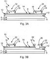
Figures 3A to 3D show a method of making a semiconductor device according to an embodiment of this disclosure. In this example, thedevice 10 comprises a HEMT having a Schottky gate contact, although it will be appreciated that processes similar to that described here may also be used to form a MISHEMT or Schottky diode. The method ofFigures 3A to 3D may be used to make adevice 10 including at least one contact of the kind shown in, for instance,Figure 1 . In this example, the contact ofFigure 1 forms adrain contact 34 of thedevice 10 to be manufactured. - In a first step, as shown in
Figure 3A , the method may include providing asubstrate 2. Thesubstrate 2 may be of the kind described above in relation toFigure 1 . - The
substrate 2 may, for instance, be a silicon substrate, although it is also envisaged that thesubstrate 2 may comprise a ceramic or glass. Thesubstrate 2 has anAlGaN layer 8 located on aGaN layer 6. A number ofbuffer layers 4 comprising GaN may be located between the GaN layer and the underlying part of thesubstrate 2. As noted previously, thesebuffer layers 4 may form a super lattice that matches the lattice of theGaN layer 6 to underlying part of thesubstrate 2. In some examples, a GaN cap layer may be located on the AlGaN layer 8 (not shown in the Figures). In the present example, isolation regions 12 (e.g. trenches filled with dielectric or implanted regions) are provided for isolating the HEMT from other electrical devices on thesubstrate 2. - A
dielectric layer 14 may be deposited on a major surface of the substrate, e.g. on a surface of theAlGaN layer 8 or any GaN cap layer that may be provided on theAlGaN layer 8. As noted previously, thedielectric layer 14 may act as a passivation layer. Thedielectric layer 14 may comprise, for instance, SiN, SiOx or AlOx. - Next,
openings 16 may be formed in thedielectric layer 14. Theseopenings 16 may allow access to the underlying layers, such as theAlGaN layer 8 for the source and drain contacts of the device. Theopenings 16 may be formed by etching. - After formation of the
opening 16, a first electrically conductive material may be deposited and patterned to form theohmic contact portion 18 of asource contact 32 and adrain contact 34 of thedevice 10. This step may also include depositing and patterning layers 22 on thesource contact 32 anddrain contact 34, which may act as a diffusion barrier. As noted previously, the first electrically conductive material that forms theohmic contact portion 18 of thesource contact 32 and thedrain contact 34 may comprise, for instance, comprise Ti/Al, while thelayers 22 of thesource contact 32 and thedrain contact 34 may, for instance, comprise TiW(N). - In a next step, shown in
Figure 3B , a masking and etching step (e.g. a dry etch) may be used to etch atrench 36 in thedrain contact 34. Thetrench 36 may be located in a central part of thedrain contact 34. Thetrench 36 may extend through theohmic contact portion 18 and thelayer 22. Thetrench 36 extends through theAlGaN layer 8 and any GaN cap layer that may be located on theAlGaN layer 8. Thetrench 36 further extends into theGaN layer 6. - In a next step shown in
Figure 3C , afurther opening 15 may be formed (e.g. by etching) in thedielectric layer 14, to allow a Schottky gate contact of thedevice 10 to be formed. Theopening 15 may be located between thesource contact 32 and thedrain contact 34 on the major surface of thesubstrate 2. - In a next step shown in
Figure 3D , a second electrically conductive material may be deposited and patterned. As noted previously, the second electrically conductive material may, for instance, comprise Ni, Pd, Pt or TiW(N). - The deposition and patterning of the second electrically conductive material may result in a
drain contact 34 that is of the kind described above in relation toFigure 1 . In the present example, the second electrically conductive material is also used to form theSchottky gate electrode 40 of the HEMT of thedevice 10. In this way, the of process steps required to manufacture thedevice 10 may be reduced, since separate deposition steps need not be provided for forming the second electricallyconductive material 50 of thecontact 34 and theSchottky gate electrode 40. Nevertheless, if it is still desired to use a different electrically conductive materials for theSchottky gate electrode 40 and thecontact 34, then different deposition step may still be used. -
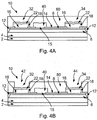
Figures 4A to 4D show a method of making a semiconductor device according to another embodiment of this disclosure. In this example, thedevice 10 comprises a HEMT having a Schottky gate contact, although it will be appreciated that processes similar to that described here may also be used to form a MISHEMT or Schottky diode. The method ofFigures 4A to 4D may be used to make adevice 10 including at least one contact of the kind shown in, for instance,Figure 2 . In this example, the contact ofFigure 2 forms adrain contact 34 of thedevice 10 to be manufactured. - In a first step, as shown in
Figure 4A , the method may include providing asubstrate 2. Thesubstrate 2 may be of the kind described above in relation toFigures 1 to 3 . - The
substrate 2 may, for instance, be a silicon substrate, although it is also envisaged that thesubstrate 2 may comprise a ceramic or glass. Thesubstrate 2 has anAlGaN layer 8 located on aGaN layer 6. A number ofbuffer layers 4 comprising GaN may be located between the GaN layer and the underlying part of thesubstrate 2. As noted previously, thesebuffer layers 4 may form a super lattice that matches the lattice of theGaN layer 6 to underlying part of thesubstrate 2. In some examples, a GaN cap layer may be located on the AlGaN layer 8 (not shown in the Figures). In the present example, thesubstrate 2 includes isolation regions 12 (e.g. trenches filled with dielectric) for isolating the HEMT from other parts of thesubstrate 2. - A
dielectric layer 14 may be deposited on a major surface of the substrate, e.g. on a surface of theAlGaN layer 8 or any GaN cap layer that may be provided on theAlGaN layer 8. As noted previously, thedielectric layer 14 may act as a passivation layer. Thedielectric layer 14 may comprise, for instance, SiN, SiOx or AlOx. - Next,
openings 16 may be formed in thedielectric layer 14. Theseopenings 16 may allow access to the underlying layers, such as theAlGaN layer 8 for the source and drain contacts of the device. Theopenings 16 may be formed by etching. - After formation of the
opening 16, a first electrically conductive material may be deposited and patterned to form theohmic contact portions 18 of asource contact 32 and adrain contact 34 of thedevice 10. This step may also include depositing and patterning layers 22 on thesource contact 32 anddrain contact 34. As noted previously, the first electrically conductive material that forms theohmic contact portions 18 of thesource contact 32 and thedrain contact 34 may comprise, for instance, comprise Ti/Al, while thelayers 22 of thesource contact 32 and thedrain contact 34 may, for instance, comprise TiW(N). - Next, a
further opening 15 may be formed (e.g. by etching) in thedielectric layer 14, to allow a Schottky gate contact of thedevice 10 to be formed. Theopening 15 may be located between thesource contact 32 and thedrain contact 34 on the major surface of thesubstrate 2. After theopening 15 is formed, an electrically conductive material may be deposited and patterned to form theSchottky gate contact 40 of the HEMT. The electrically conductive material of theSchottky gate contact 40 may, for instance, comprise Ni. - Next a
dielectric layer 60 may be deposited, e.g. by Plasma Enhanced Chemical Vapour Deposition (PECVD). Thelayer 60 may, for instance, comprise SiN. Thelayer 60 may have a thickness of around 100nm. - In a next step shown in
Figure 4B ,openings layer 60, to obtain access to theunderlying source contact 32 and thedrain contact 34. - In a next step shown in
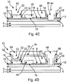
Figure 4C , a masking and etching step (e.g. a dry etch) may be used to etch atrench 38 in thedrain contact 34. Thetrench 38 may be located in a central part of thedrain contact 34. Thetrench 36 may extend through theohmic contact portion 18 and thelayer 22. Thetrench 36 may further extend through theAlGaN layer 8 and any GaN cap layer that may be located on theAlGaN layer 8. Thetrench 36 may further extend into theGaN layer 6. - In a next step, a
layer 86 of a second electrically conductive material may be deposited. In this example, the second electrically conductive material comprises TiW(N), although in other examples, the second electrically conductive material may, for instance, comprise Ni, Pd or Pt. Thelayer 86 of the second electrically conductive material may have a thickness of around 100nm. Thelayer 86 of the second electrically conductive material may line thetrench 38 and/or sidewalls of the central part of the contact. Thelayer 86 may also cover an upper surface of thelayer 22 of thedrain contact 34. Thelayer 86 may further cover an upper surface of thelayer 22 of thesource contact 32 and an upper surface of thelayer 60. - Thereafter, a third electrically
conductive material 88, such as Al, may be deposited on thelayer 86. In some examples, around 1µm of the third electrically conductive material may be deposited on thelayer 86. Note that in the present example, theSchottky gate electrode 40 may be of a different material to the second electrically conductive material. - After the second and third electrically conductive materials have been deposited, they may be patterned to result in the structure shown in
Figure 4D . The second electrically conductive material may thus form alayer 86 that lines the trench in thedrain contact 34 and may also form alayer 82 that covers an upper surface of thelayer 22 of thesource contact 32. Apart 19 of thelayer 82 may extend above the gate. Thelayer 82 may itself be covered by aportion 84 of the third electrically conductive material. Thepart 19 of thelayer 82, and the overlyingportion 84 may thus form a source field plate for thedevice 10. Note that the structure of thedrain contact 34 inFigure 4D is of the kind described above in relation toFigure 2 . Note that thedielectric layer 60 may serve to separate and isolate thepart 19 of thelayer 82 and the overlyingportion 84 from the underlying parts of thedevice 10, such as thegate contact 40. -
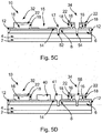
Figures 5A to 5D show a method of making a semiconductor device according to a further embodiment of this disclosure. In this example, thedevice 10 comprises a HEMT having a Schottky gate contact, although it will be appreciated that processes similar to that described here may also be used to form a MISHEMT or Schottky diode. In this example, the contact of the HEMT that includes a trench of the kind described herein is the drain contact. - In a first step, as shown in
Figure 5A , the method may include providing asubstrate 2. Thesubstrate 2 may be of the kind described above in relation toFigures 1 to 4 . - The
substrate 2 may, for instance, be a silicon substrate, although it is also envisaged that thesubstrate 2 may comprise a ceramic or glass. Thesubstrate 2 has anAlGaN layer 8 located on aGaN layer 6. A number ofbuffer layers 4 comprising e.g. GaN and AlGaN may be located between the GaN layer and the underlying part of thesubstrate 2. As noted previously, thesebuffer layers 4 may form a super lattice that matches the lattice of theGaN layer 6 to underlying part of thesubstrate 2. In some examples, a GaN cap layer may be located on the AlGaN layer 8 (not shown in the Figures). In the present example, isolation regions 12 (e.g. trenches filled with dielectric or implanted regions) are provided for isolating the HEMT from other electrical devices on thesubstrate 2. - A
dielectric layer 14 may be deposited on a major surface of the substrate, e.g. on a surface of theAlGaN layer 8 or any GaN cap layer that may be provided on theAlGaN layer 8. As noted previously, thedielectric layer 14 may act as a passivation layer. Thedielectric layer 14 may comprise, for instance, SiN, SiOx or AlOx. - Next,
openings 16 may be formed in thedielectric layer 14. Theseopenings 16 may allow access to the underlying layers, such as theAlGaN layer 8 for the source and drain contacts of the device. Theopenings 16 may be formed by etching. - After formation of the
openings 16, a first electrically conductive material may be deposited and patterned to form theohmic contact portions 18 of asource contact 32 and adrain contact 34 of thedevice 10. This step may also include depositing and patterning layers 22 on thesource contact 32 anddrain contact 34, as described previously. As also noted previously, the first electrically conductive material that forms theohmic contact portions 18 of thesource contact 32 and thedrain contact 34 may comprise, for instance, comprise Ti/Al, while thelayers 22 of thesource contact 32 and thedrain contact 34 may, for instance, comprise TiW(N). - In a next step shown in
Figure 5B ,further openings dielectric layer 14. Theopening 15 may, as described in relation to previous embodiments, allow a Schottky gate contact of thedevice 10 to be formed. Theopening 15 may be located between thesource contact 32 and thedrain contact 34 on the major surface of thesubstrate 2. One ormore openings 17 may allow one of more islands to be formed between the gate contact and the drain contact of the device, as described in more detail below. - In a next step shown in
Figure 5C , a masking and etching process may be used to form a number of trenches. These trenches may include atrench 54 that extends through thedrain contact 34 and into theGaN layer 6 as described above in relation to the preceding embodiments. In the present example, one ormore trenches 52 may also be etched through the one ormore openings 17 in thedielectric layer 14. Thetrenches 52 may extend down into thesubstrate 2 from the major surface thereof in a manner similar to that already described in relation to thetrench 54 of thedrain contact 34. - In a next step, a second electrically conductive material may be deposited and patterned, resulting in the device shown in
Figure 5D . In the present example, the second electrically conductive material comprises Ni, although as noted previously, it is envisaged that the second electrically conductive material may comprise, for instance, Pd, Pt or TiW(N). - As can be seen in
Figure 5D , the second electrically conductive material may at least partially fill thetrench 54 of the drain contact 34 (as indicated usingreference numeral 58 inFigure 5D ), resulting in a drain contact similar to the contacts described above in relation to the earlier embodiments. In some examples, the second electrically conductive material may be provided in the form of a layer that lines thetrench 54 as described above in relation toFigure 2 . - Another part of the deposited and patterned second electrically conductive material, which is aligned with the
opening 15 in thedielectric layer 14, may form aSchottky gate electrode 40 of thedevice 10. - A further part of the deposited and patterned second electrically conductive material may at least partially fill each of the one or
more trenches 52 described above in relation toFigure 5C . This may result in the formation of one ormore islands 41 located between the gate contact and thedrain contact 34, each island including a trench extending down into thesubstrate 2 from the major surface, with each trench being at least partially filled with the second electrically conductive material. In examples where the second electrically conductive material is provided in the form of a layer as noted above, the layer may also line thetrenches 52. The remainder of thetrench 54 and/or thetrenches 52 may be filled with a third electrically conductive material such as Al. - As may be seen in
Figure 5D , a part of the second electrically conductive material of eachisland 41 may extend out of thetrenches 52 and above the major surface of the substrate 2 (e.g. it may extend over the surface of the dielectric layer 14). Theislands 41 may be electrically connected to thedrain contact 32. - The
islands 41 may provide a further route for holes located in theGaN layer 6 to exit thedevice 10. - The
islands 41 and their associatedtrenches 52 may, when viewed from above the major surface of thesubstrate 2 be shaped as dots or stripes. The islands may be arranged in an array. For instance, the array may comprise on or more rows of substantially equally spaced islands. - In each of the examples described above in relation to
Figures 3 to 5 , it is envisaged that theopening 15 in the dielectric layer may be omitted, allowing a MISHEMT to be formed without necessarily requiring any other significant modification of the manufacturing process. - Accordingly, there has been described a semiconductor device and a method of making the same. The device includes a substrate having an AlGaN layer located on a GaN layer for forming a two dimensional electron gas at an interface between the AlGaN layer and the GaN layer. The device also includes a plurality of contacts. At least one of the contacts includes an ohmic contact portion located on a major surface of the substrate. The ohmic contact portion comprises a first electrically conductive material. The at least one of the contacts also includes a trench extending down into the substrate from the major surface. The trench passes through the AlGaN layer and into the GaN layer. The trench is at least partially filled with a second electrically conductive material. The second electrically conductive material is a different electrically conductive material to the first electrically conductive material.
- Although particular embodiments of this disclosure have been described, it will be appreciated that many modifications/additions and/or substitutions may be made within the scope of the claims.
Claims (15)
- A semiconductor device comprising:a substrate having an AlGaN layer located on a GaN layer for forming a two dimensional electron gas at an interface between the AlGaN layer and the GaN layer; anda plurality of contacts,wherein at least one of the contacts comprises:an ohmic contact portion located on a major surface of the substrate, wherein the ohmic contact portion comprises a first electrically conductive material; anda trench extending down into the substrate from the major surface, wherein the trench passes through the AlGaN layer and into the GaN layer, wherein the trench is at least partially filled with a second electrically conductive material, and wherein the second electrically conductive material is a different electrically conductive material to the first electrically conductive material.
- The semiconductor device of claim 1, wherein said at least one of the contacts includes a central part aligned with the trench, wherein the central part is at least partially filled with the second electrically conductive material and wherein the central part is substantially surrounded by the ohmic contact portion when viewed from above the major surface.
- The semiconductor device of claim, comprising a single contiguous portion of said second electrically conductive material at least partially filling the central part of the contact and the trench.
- The semiconductor device of claim 2 or claim 3, wherein said second electrically conductive material comprises a layer that lines at least the trench.
- The semiconductor device of any preceding claim, wherein the substrate further includes a GaN cap layer located on the AlGaN layer, and wherein the trench of said at least one of the contacts passes through the GaN cap layer.
- The semiconductor device of any preceding claim, wherein the device comprises a High Electron Mobility Transistor (HEMT) comprising a gate contact located between a source contact and a drain contact, and wherein said at least one of the contacts is a drain contact of the HEMT.
- The semiconductor device of any of claims 1 to 5, wherein the device comprises a Schottky diode and wherein said at least one of the contacts is a cathode of the Schottky diode.
- The semiconductor device of claim 6 comprising at least one island located between the drain and the gate, wherein each island includes a trench extending down into the substrate from the major surface, wherein the trench passes through the AlGaN layer and into the GaN layer, wherein the trench is at least partially filled with said second electrically conductive material.
- The semiconductor device of any of claims 6 to 8, wherein the gate of the HEMT or an anode of the Schottky diode contact comprises said second electrically conductive material.
- The semiconductor device of any preceding claim, wherein the first electrically conductive material comprises an alloy of Ti/Al and/or wherein the second electrically conductive material comprises Ni, Pd, Pt or TiWN.
- A method of making a semiconductor device, the method comprising:providing a substrate having an AlGaN layer located on a GaN layer for forming a two dimensional electron gas at an interface between the AlGaN layer and the GaN layer; andforming a plurality of contacts of the device,wherein forming at least one of said contacts comprises:depositing a first electrically conductive material on a major surface of the substrate to form an ohmic contact portion;forming a trench extending down into the substrate from the major surface, wherein the trench passes through the AlGaN layer and into the GaN layer; andat least partially filling the trench with a second electrically conductive material,wherein the second electrically conductive material is a different electrically conductive material to the first electrically conductive material.
- The method of claim 11, comprising:removing at least part of the first electrically conductive material of the at least one said contact to form an opening in the ohmic contact portion, wherein the opening exposes a part of the major surface;forming the trench in the part of the major surface exposed by the opening in the ohmic contact portion; andat least partially filling the trench and the opening in the ohmic contact portion with said second electrically conductive material.
- The method of claim 12, wherein the part of the first electrically conductive material of the at least one said contact that is removed to form said opening in the ohmic contact portion comprises a central part of said contact, and wherein after said at least partially filling the trench and the opening in the ohmic contact portion with said second electrically conductive material, the central part is substantially surrounded by the ohmic contact portion when viewed from above the major surface.
- The method of claim 12 or claim 13, wherein the semiconductor device comprises a High Electron Mobility Transistor (HEMT), the method comprising forming a gate contact of the HEMT located between a source contact and a drain contact of the HEMT.
- The method of claim 14, further comprising forming at least one island located between the drain contact and the gate contact by:forming one or more trenches extending down into the substrate from the major surface, wherein each trench passes through the AlGaN layer and into the GaN layer; andat least partially filling each trench with said second electrically conductive material.
Priority Applications (3)
| Application Number | Priority Date | Filing Date | Title |
|---|---|---|---|
| EP15196730.4A EP3174102B1 (en) | 2015-11-27 | 2015-11-27 | Semiconductor device and method of making a semiconductor device |
| US15/356,509 US10403747B2 (en) | 2015-11-27 | 2016-11-18 | Gallium nitride/ aluminum gallium nitride semiconductor device and method of making a gallium nitride/ aluminum gallium nitride semiconductor device |
| CN201611041068.XA CN106816466B (en) | 2015-11-27 | 2016-11-22 | Semiconductor device and method of making semiconductor device |
Applications Claiming Priority (1)
| Application Number | Priority Date | Filing Date | Title |
|---|---|---|---|
| EP15196730.4A EP3174102B1 (en) | 2015-11-27 | 2015-11-27 | Semiconductor device and method of making a semiconductor device |
Publications (2)
| Publication Number | Publication Date |
|---|---|
| EP3174102A1 true EP3174102A1 (en) | 2017-05-31 |
| EP3174102B1 EP3174102B1 (en) | 2022-09-28 |
Family
ID=54705518
Family Applications (1)
| Application Number | Title | Priority Date | Filing Date |
|---|---|---|---|
| EP15196730.4A Active EP3174102B1 (en) | 2015-11-27 | 2015-11-27 | Semiconductor device and method of making a semiconductor device |
Country Status (3)
| Country | Link |
|---|---|
| US (1) | US10403747B2 (en) |
| EP (1) | EP3174102B1 (en) |
| CN (1) | CN106816466B (en) |
Families Citing this family (7)
| Publication number | Priority date | Publication date | Assignee | Title |
|---|---|---|---|---|
| CN109671776A (en) * | 2018-12-24 | 2019-04-23 | 广东省半导体产业技术研究院 | Semiconductor device and method of manufacturing the same |
| EP4135051A1 (en) | 2021-08-10 | 2023-02-15 | Infineon Technologies Austria AG | Lateral iii/v heterostructure field effect transistor |
| CN113809173B (en) * | 2021-09-16 | 2024-11-22 | 深圳市承恩热视科技有限公司 | Millimeter wave switch chip |
| US12581701B2 (en) * | 2021-10-18 | 2026-03-17 | Globalfoundries U.S. Inc. | Device with dual isolation structure |
| US12349433B2 (en) | 2021-12-20 | 2025-07-01 | Nxp Usa, Inc. | Transistors with self-aligned source-connected field plates |
| US12148820B2 (en) | 2021-12-20 | 2024-11-19 | Nxp B.V. | Transistors with source-connected field plates |
| US12342560B2 (en) | 2021-12-20 | 2025-06-24 | Nxp Usa, Inc. | Transistors with source-connected field plates |
Citations (2)
| Publication number | Priority date | Publication date | Assignee | Title |
|---|---|---|---|---|
| US20080284022A1 (en) * | 2006-12-12 | 2008-11-20 | Sanken Electric Co., Ltd. | Semiconductor device and method for manufacturing the same |
| US20130248874A1 (en) * | 2012-03-26 | 2013-09-26 | Kabushiki Kaisha Toshiba | Nitride semiconductor device |
Family Cites Families (8)
| Publication number | Priority date | Publication date | Assignee | Title |
|---|---|---|---|---|
| JP4700125B2 (en) * | 2009-07-30 | 2011-06-15 | 住友電気工業株式会社 | Semiconductor device and manufacturing method thereof |
| US8492773B2 (en) * | 2010-04-23 | 2013-07-23 | Intersil Americas Inc. | Power devices with integrated protection devices: structures and methods |
| JP5848680B2 (en) | 2011-11-22 | 2016-01-27 | ルネサスエレクトロニクス株式会社 | Semiconductor device and manufacturing method of semiconductor device |
| JP5841417B2 (en) * | 2011-11-30 | 2016-01-13 | 株式会社日立製作所 | Nitride semiconductor diode |
| KR101608494B1 (en) * | 2011-12-19 | 2016-04-01 | 인텔 코포레이션 | Group iii-n transistors for system on chip(soc) architecture integrating power management and radio frequency circuits |
| US8963162B2 (en) * | 2011-12-28 | 2015-02-24 | Taiwan Semiconductor Manufacturing Company, Ltd. | High electron mobility transistor |
| EP2793265B1 (en) | 2013-04-15 | 2017-06-07 | Nexperia B.V. | Semiconductor device and manufacturing method |
| EP2953167A1 (en) | 2014-06-05 | 2015-12-09 | Nxp B.V. | Semiconductor heterojunction device |
-
2015
- 2015-11-27 EP EP15196730.4A patent/EP3174102B1/en active Active
-
2016
- 2016-11-18 US US15/356,509 patent/US10403747B2/en active Active
- 2016-11-22 CN CN201611041068.XA patent/CN106816466B/en active Active
Patent Citations (2)
| Publication number | Priority date | Publication date | Assignee | Title |
|---|---|---|---|---|
| US20080284022A1 (en) * | 2006-12-12 | 2008-11-20 | Sanken Electric Co., Ltd. | Semiconductor device and method for manufacturing the same |
| US20130248874A1 (en) * | 2012-03-26 | 2013-09-26 | Kabushiki Kaisha Toshiba | Nitride semiconductor device |
Non-Patent Citations (1)
| Title |
|---|
| CHUNHUA ZHOU ET AL: "Self-protected GaN power devices with reverse drain blocking and forward current limiting capabilities", POWER SEMICONDUCTOR DEVICES&IC'S (ISPSD), 2010 22ND INTERNATIONAL SYMPOSIUM ON, IEEE, PISCATAWAY, NJ, USA, 6 June 2010 (2010-06-06), pages 343 - 346, XP031729050, ISBN: 978-1-4244-7718-0 * |
Also Published As
| Publication number | Publication date |
|---|---|
| US20170154988A1 (en) | 2017-06-01 |
| CN106816466B (en) | 2021-03-16 |
| EP3174102B1 (en) | 2022-09-28 |
| US10403747B2 (en) | 2019-09-03 |
| CN106816466A (en) | 2017-06-09 |
Similar Documents
| Publication | Publication Date | Title |
|---|---|---|
| US10403747B2 (en) | Gallium nitride/ aluminum gallium nitride semiconductor device and method of making a gallium nitride/ aluminum gallium nitride semiconductor device | |
| US11854926B2 (en) | Semiconductor device with a passivation layer and method for producing thereof | |
| US9576841B2 (en) | Semiconductor device and manufacturing method | |
| CN105684134B (en) | Gallium nitride transistors with polysilicon layers for creating additional features | |
| US20170162429A1 (en) | Semiconductor devices with back surface isolation | |
| TW201618276A (en) | Improved GaN structure | |
| US9324816B2 (en) | Semiconductor device | |
| US9276075B2 (en) | Semiconductor device having vertical MOSFET structure that utilizes a trench-type gate electrode and method of producing the same | |
| CN109872974A (en) | Semiconductor devices with integrated PN diode temperature sensor | |
| US20140210052A1 (en) | Semiconductor Device and Method for Manufacturing a Semiconductor Device | |
| US9490355B2 (en) | Silicon carbide static induction transistor and process for making a silicon carbide static induction transistor | |
| JP2018137389A (en) | Semiconductor device | |
| US20230042721A1 (en) | Semiconductor device and manufacturing method of semiconductor device | |
| EP3499549B1 (en) | Semiconductor device | |
| US20150263147A1 (en) | Semiconductor device | |
| US10615292B2 (en) | High voltage silicon carbide Schottky diode flip chip array | |
| CN207781612U (en) | Power semiconductor | |
| JP2026016298A (en) | semiconductor elements | |
| KR20260036942A (en) | Semiconductor device | |
| KR20160100524A (en) | nitride-based insulated gate bipolar transistor | |
| WO2012172904A1 (en) | Power device, and method for producing power device |
Legal Events
| Date | Code | Title | Description |
|---|---|---|---|
| PUAI | Public reference made under article 153(3) epc to a published international application that has entered the european phase |
Free format text: ORIGINAL CODE: 0009012 |
|
| STAA | Information on the status of an ep patent application or granted ep patent |
Free format text: STATUS: THE APPLICATION HAS BEEN PUBLISHED |
|
| AK | Designated contracting states |
Kind code of ref document: A1 Designated state(s): AL AT BE BG CH CY CZ DE DK EE ES FI FR GB GR HR HU IE IS IT LI LT LU LV MC MK MT NL NO PL PT RO RS SE SI SK SM TR |
|
| AX | Request for extension of the european patent |
Extension state: BA ME |
|
| STAA | Information on the status of an ep patent application or granted ep patent |
Free format text: STATUS: REQUEST FOR EXAMINATION WAS MADE |
|
| 17P | Request for examination filed |
Effective date: 20171130 |
|
| RBV | Designated contracting states (corrected) |
Designated state(s): AL AT BE BG CH CY CZ DE DK EE ES FI FR GB GR HR HU IE IS IT LI LT LU LV MC MK MT NL NO PL PT RO RS SE SI SK SM TR |
|
| STAA | Information on the status of an ep patent application or granted ep patent |
Free format text: STATUS: EXAMINATION IS IN PROGRESS |
|
| 17Q | First examination report despatched |
Effective date: 20190410 |
|
| GRAP | Despatch of communication of intention to grant a patent |
Free format text: ORIGINAL CODE: EPIDOSNIGR1 |
|
| STAA | Information on the status of an ep patent application or granted ep patent |
Free format text: STATUS: GRANT OF PATENT IS INTENDED |
|
| RIC1 | Information provided on ipc code assigned before grant |
Ipc: H01L 29/40 20060101ALN20220627BHEP Ipc: H01L 29/20 20060101ALN20220627BHEP Ipc: H01L 29/423 20060101ALN20220627BHEP Ipc: H01L 29/45 20060101ALI20220627BHEP Ipc: H01L 29/417 20060101ALI20220627BHEP Ipc: H01L 21/338 20060101ALI20220627BHEP Ipc: H01L 29/778 20060101AFI20220627BHEP |
|
| INTG | Intention to grant announced |
Effective date: 20220711 |
|
| RAP3 | Party data changed (applicant data changed or rights of an application transferred) |
Owner name: NEXPERIA B.V. |
|
| GRAS | Grant fee paid |
Free format text: ORIGINAL CODE: EPIDOSNIGR3 |
|
| GRAA | (expected) grant |
Free format text: ORIGINAL CODE: 0009210 |
|
| STAA | Information on the status of an ep patent application or granted ep patent |
Free format text: STATUS: THE PATENT HAS BEEN GRANTED |
|
| AK | Designated contracting states |
Kind code of ref document: B1 Designated state(s): AL AT BE BG CH CY CZ DE DK EE ES FI FR GB GR HR HU IE IS IT LI LT LU LV MC MK MT NL NO PL PT RO RS SE SI SK SM TR |
|
| REG | Reference to a national code |
Ref country code: GB Ref legal event code: FG4D |
|
| REG | Reference to a national code |
Ref country code: CH Ref legal event code: EP |
|
| REG | Reference to a national code |
Ref country code: AT Ref legal event code: REF Ref document number: 1521815 Country of ref document: AT Kind code of ref document: T Effective date: 20221015 |
|
| REG | Reference to a national code |
Ref country code: DE Ref legal event code: R096 Ref document number: 602015080959 Country of ref document: DE |
|
| REG | Reference to a national code |
Ref country code: IE Ref legal event code: FG4D |
|
| REG | Reference to a national code |
Ref country code: LT Ref legal event code: MG9D |
|
| PG25 | Lapsed in a contracting state [announced via postgrant information from national office to epo] |
Ref country code: SE Free format text: LAPSE BECAUSE OF FAILURE TO SUBMIT A TRANSLATION OF THE DESCRIPTION OR TO PAY THE FEE WITHIN THE PRESCRIBED TIME-LIMIT Effective date: 20220928 Ref country code: RS Free format text: LAPSE BECAUSE OF FAILURE TO SUBMIT A TRANSLATION OF THE DESCRIPTION OR TO PAY THE FEE WITHIN THE PRESCRIBED TIME-LIMIT Effective date: 20220928 Ref country code: NO Free format text: LAPSE BECAUSE OF FAILURE TO SUBMIT A TRANSLATION OF THE DESCRIPTION OR TO PAY THE FEE WITHIN THE PRESCRIBED TIME-LIMIT Effective date: 20221228 Ref country code: LV Free format text: LAPSE BECAUSE OF FAILURE TO SUBMIT A TRANSLATION OF THE DESCRIPTION OR TO PAY THE FEE WITHIN THE PRESCRIBED TIME-LIMIT Effective date: 20220928 Ref country code: LT Free format text: LAPSE BECAUSE OF FAILURE TO SUBMIT A TRANSLATION OF THE DESCRIPTION OR TO PAY THE FEE WITHIN THE PRESCRIBED TIME-LIMIT Effective date: 20220928 Ref country code: FI Free format text: LAPSE BECAUSE OF FAILURE TO SUBMIT A TRANSLATION OF THE DESCRIPTION OR TO PAY THE FEE WITHIN THE PRESCRIBED TIME-LIMIT Effective date: 20220928 |
|
| REG | Reference to a national code |
Ref country code: NL Ref legal event code: MP Effective date: 20220928 |
|
| REG | Reference to a national code |
Ref country code: AT Ref legal event code: MK05 Ref document number: 1521815 Country of ref document: AT Kind code of ref document: T Effective date: 20220928 |
|
| PG25 | Lapsed in a contracting state [announced via postgrant information from national office to epo] |
Ref country code: HR Free format text: LAPSE BECAUSE OF FAILURE TO SUBMIT A TRANSLATION OF THE DESCRIPTION OR TO PAY THE FEE WITHIN THE PRESCRIBED TIME-LIMIT Effective date: 20220928 Ref country code: GR Free format text: LAPSE BECAUSE OF FAILURE TO SUBMIT A TRANSLATION OF THE DESCRIPTION OR TO PAY THE FEE WITHIN THE PRESCRIBED TIME-LIMIT Effective date: 20221229 |
|
| PG25 | Lapsed in a contracting state [announced via postgrant information from national office to epo] |
Ref country code: SM Free format text: LAPSE BECAUSE OF FAILURE TO SUBMIT A TRANSLATION OF THE DESCRIPTION OR TO PAY THE FEE WITHIN THE PRESCRIBED TIME-LIMIT Effective date: 20220928 Ref country code: RO Free format text: LAPSE BECAUSE OF FAILURE TO SUBMIT A TRANSLATION OF THE DESCRIPTION OR TO PAY THE FEE WITHIN THE PRESCRIBED TIME-LIMIT Effective date: 20220928 Ref country code: PT Free format text: LAPSE BECAUSE OF FAILURE TO SUBMIT A TRANSLATION OF THE DESCRIPTION OR TO PAY THE FEE WITHIN THE PRESCRIBED TIME-LIMIT Effective date: 20230130 Ref country code: ES Free format text: LAPSE BECAUSE OF FAILURE TO SUBMIT A TRANSLATION OF THE DESCRIPTION OR TO PAY THE FEE WITHIN THE PRESCRIBED TIME-LIMIT Effective date: 20220928 Ref country code: CZ Free format text: LAPSE BECAUSE OF FAILURE TO SUBMIT A TRANSLATION OF THE DESCRIPTION OR TO PAY THE FEE WITHIN THE PRESCRIBED TIME-LIMIT Effective date: 20220928 Ref country code: AT Free format text: LAPSE BECAUSE OF FAILURE TO SUBMIT A TRANSLATION OF THE DESCRIPTION OR TO PAY THE FEE WITHIN THE PRESCRIBED TIME-LIMIT Effective date: 20220928 |
|
| PG25 | Lapsed in a contracting state [announced via postgrant information from national office to epo] |
Ref country code: SK Free format text: LAPSE BECAUSE OF FAILURE TO SUBMIT A TRANSLATION OF THE DESCRIPTION OR TO PAY THE FEE WITHIN THE PRESCRIBED TIME-LIMIT Effective date: 20220928 Ref country code: PL Free format text: LAPSE BECAUSE OF FAILURE TO SUBMIT A TRANSLATION OF THE DESCRIPTION OR TO PAY THE FEE WITHIN THE PRESCRIBED TIME-LIMIT Effective date: 20220928 Ref country code: IS Free format text: LAPSE BECAUSE OF FAILURE TO SUBMIT A TRANSLATION OF THE DESCRIPTION OR TO PAY THE FEE WITHIN THE PRESCRIBED TIME-LIMIT Effective date: 20230128 Ref country code: EE Free format text: LAPSE BECAUSE OF FAILURE TO SUBMIT A TRANSLATION OF THE DESCRIPTION OR TO PAY THE FEE WITHIN THE PRESCRIBED TIME-LIMIT Effective date: 20220928 |
|
| REG | Reference to a national code |
Ref country code: DE Ref legal event code: R097 Ref document number: 602015080959 Country of ref document: DE |
|
| PG25 | Lapsed in a contracting state [announced via postgrant information from national office to epo] |
Ref country code: NL Free format text: LAPSE BECAUSE OF FAILURE TO SUBMIT A TRANSLATION OF THE DESCRIPTION OR TO PAY THE FEE WITHIN THE PRESCRIBED TIME-LIMIT Effective date: 20220928 Ref country code: MC Free format text: LAPSE BECAUSE OF FAILURE TO SUBMIT A TRANSLATION OF THE DESCRIPTION OR TO PAY THE FEE WITHIN THE PRESCRIBED TIME-LIMIT Effective date: 20220928 Ref country code: AL Free format text: LAPSE BECAUSE OF FAILURE TO SUBMIT A TRANSLATION OF THE DESCRIPTION OR TO PAY THE FEE WITHIN THE PRESCRIBED TIME-LIMIT Effective date: 20220928 |
|
| REG | Reference to a national code |
Ref country code: CH Ref legal event code: PL |
|
| REG | Reference to a national code |
Ref country code: BE Ref legal event code: MM Effective date: 20221130 |
|
| PG25 | Lapsed in a contracting state [announced via postgrant information from national office to epo] |
Ref country code: LI Free format text: LAPSE BECAUSE OF NON-PAYMENT OF DUE FEES Effective date: 20221130 Ref country code: DK Free format text: LAPSE BECAUSE OF FAILURE TO SUBMIT A TRANSLATION OF THE DESCRIPTION OR TO PAY THE FEE WITHIN THE PRESCRIBED TIME-LIMIT Effective date: 20220928 Ref country code: CH Free format text: LAPSE BECAUSE OF NON-PAYMENT OF DUE FEES Effective date: 20221130 |
|
| PLBE | No opposition filed within time limit |
Free format text: ORIGINAL CODE: 0009261 |
|
| STAA | Information on the status of an ep patent application or granted ep patent |
Free format text: STATUS: NO OPPOSITION FILED WITHIN TIME LIMIT |
|
| GBPC | Gb: european patent ceased through non-payment of renewal fee |
Effective date: 20221228 |
|
| PG25 | Lapsed in a contracting state [announced via postgrant information from national office to epo] |
Ref country code: LU Free format text: LAPSE BECAUSE OF NON-PAYMENT OF DUE FEES Effective date: 20221127 |
|
| 26N | No opposition filed |
Effective date: 20230629 |
|
| PG25 | Lapsed in a contracting state [announced via postgrant information from national office to epo] |
Ref country code: IE Free format text: LAPSE BECAUSE OF NON-PAYMENT OF DUE FEES Effective date: 20221127 Ref country code: GB Free format text: LAPSE BECAUSE OF NON-PAYMENT OF DUE FEES Effective date: 20221228 |
|
| PG25 | Lapsed in a contracting state [announced via postgrant information from national office to epo] |
Ref country code: SI Free format text: LAPSE BECAUSE OF FAILURE TO SUBMIT A TRANSLATION OF THE DESCRIPTION OR TO PAY THE FEE WITHIN THE PRESCRIBED TIME-LIMIT Effective date: 20220928 Ref country code: FR Free format text: LAPSE BECAUSE OF NON-PAYMENT OF DUE FEES Effective date: 20221128 Ref country code: BE Free format text: LAPSE BECAUSE OF NON-PAYMENT OF DUE FEES Effective date: 20221130 |
|
| PG25 | Lapsed in a contracting state [announced via postgrant information from national office to epo] |
Ref country code: HU Free format text: LAPSE BECAUSE OF FAILURE TO SUBMIT A TRANSLATION OF THE DESCRIPTION OR TO PAY THE FEE WITHIN THE PRESCRIBED TIME-LIMIT; INVALID AB INITIO Effective date: 20151127 |
|
| PG25 | Lapsed in a contracting state [announced via postgrant information from national office to epo] |
Ref country code: CY Free format text: LAPSE BECAUSE OF FAILURE TO SUBMIT A TRANSLATION OF THE DESCRIPTION OR TO PAY THE FEE WITHIN THE PRESCRIBED TIME-LIMIT Effective date: 20220928 |
|
| PG25 | Lapsed in a contracting state [announced via postgrant information from national office to epo] |
Ref country code: MK Free format text: LAPSE BECAUSE OF FAILURE TO SUBMIT A TRANSLATION OF THE DESCRIPTION OR TO PAY THE FEE WITHIN THE PRESCRIBED TIME-LIMIT Effective date: 20220928 Ref country code: IT Free format text: LAPSE BECAUSE OF FAILURE TO SUBMIT A TRANSLATION OF THE DESCRIPTION OR TO PAY THE FEE WITHIN THE PRESCRIBED TIME-LIMIT Effective date: 20220928 |
|
| PG25 | Lapsed in a contracting state [announced via postgrant information from national office to epo] |
Ref country code: BG Free format text: LAPSE BECAUSE OF FAILURE TO SUBMIT A TRANSLATION OF THE DESCRIPTION OR TO PAY THE FEE WITHIN THE PRESCRIBED TIME-LIMIT Effective date: 20220928 |
|
| PG25 | Lapsed in a contracting state [announced via postgrant information from national office to epo] |
Ref country code: MT Free format text: LAPSE BECAUSE OF FAILURE TO SUBMIT A TRANSLATION OF THE DESCRIPTION OR TO PAY THE FEE WITHIN THE PRESCRIBED TIME-LIMIT Effective date: 20220928 |
|
| REG | Reference to a national code |
Ref country code: DE Ref legal event code: R079 Ref document number: 602015080959 Country of ref document: DE Free format text: PREVIOUS MAIN CLASS: H01L0029778000 Ipc: H10D0030470000 |
|
| PG25 | Lapsed in a contracting state [announced via postgrant information from national office to epo] |
Ref country code: TR Free format text: LAPSE BECAUSE OF FAILURE TO SUBMIT A TRANSLATION OF THE DESCRIPTION OR TO PAY THE FEE WITHIN THE PRESCRIBED TIME-LIMIT Effective date: 20220928 |
|
| PGFP | Annual fee paid to national office [announced via postgrant information from national office to epo] |
Ref country code: DE Payment date: 20251126 Year of fee payment: 11 |