EP3172767B1 - Optoelectronic modules including an image sensor having regions optically separated from one another - Google Patents
Optoelectronic modules including an image sensor having regions optically separated from one another Download PDFInfo
- Publication number
- EP3172767B1 EP3172767B1 EP15824918.5A EP15824918A EP3172767B1 EP 3172767 B1 EP3172767 B1 EP 3172767B1 EP 15824918 A EP15824918 A EP 15824918A EP 3172767 B1 EP3172767 B1 EP 3172767B1
- Authority
- EP
- European Patent Office
- Prior art keywords
- adhesive
- image sensor
- spacer
- bridge
- module
- Prior art date
- Legal status (The legal status is an assumption and is not a legal conclusion. Google has not performed a legal analysis and makes no representation as to the accuracy of the status listed.)
- Active
Links
- 230000005693 optoelectronics Effects 0.000 title claims description 16
- 239000000853 adhesive Substances 0.000 claims description 103
- 230000001070 adhesive effect Effects 0.000 claims description 103
- 125000006850 spacer group Chemical group 0.000 claims description 65
- 238000000034 method Methods 0.000 claims description 43
- 239000000758 substrate Substances 0.000 claims description 31
- 238000004519 manufacturing process Methods 0.000 claims description 15
- 230000005499 meniscus Effects 0.000 claims description 14
- 238000011109 contamination Methods 0.000 claims description 6
- 239000000463 material Substances 0.000 claims description 6
- 239000004593 Epoxy Substances 0.000 description 56
- 230000005855 radiation Effects 0.000 description 12
- 238000001723 curing Methods 0.000 description 10
- 238000002347 injection Methods 0.000 description 9
- 239000007924 injection Substances 0.000 description 9
- 230000003287 optical effect Effects 0.000 description 7
- 238000012545 processing Methods 0.000 description 5
- 239000004205 dimethyl polysiloxane Substances 0.000 description 3
- 235000013870 dimethyl polysiloxane Nutrition 0.000 description 3
- CXQXSVUQTKDNFP-UHFFFAOYSA-N octamethyltrisiloxane Chemical compound C[Si](C)(C)O[Si](C)(C)O[Si](C)(C)C CXQXSVUQTKDNFP-UHFFFAOYSA-N 0.000 description 3
- 238000004987 plasma desorption mass spectroscopy Methods 0.000 description 3
- 229920000435 poly(dimethylsiloxane) Polymers 0.000 description 3
- 238000007789 sealing Methods 0.000 description 3
- 238000013036 cure process Methods 0.000 description 2
- 238000000151 deposition Methods 0.000 description 2
- 238000001514 detection method Methods 0.000 description 2
- 238000001746 injection moulding Methods 0.000 description 2
- 238000005259 measurement Methods 0.000 description 2
- 238000001029 thermal curing Methods 0.000 description 2
- NIXOWILDQLNWCW-UHFFFAOYSA-M Acrylate Chemical compound [O-]C(=O)C=C NIXOWILDQLNWCW-UHFFFAOYSA-M 0.000 description 1
- 238000003848 UV Light-Curing Methods 0.000 description 1
- 230000015572 biosynthetic process Effects 0.000 description 1
- 239000006229 carbon black Substances 0.000 description 1
- 238000012937 correction Methods 0.000 description 1
- 238000005520 cutting process Methods 0.000 description 1
- 230000032798 delamination Effects 0.000 description 1
- 230000008021 deposition Effects 0.000 description 1
- 125000003700 epoxy group Chemical group 0.000 description 1
- 239000000945 filler Substances 0.000 description 1
- 230000009969 flowable effect Effects 0.000 description 1
- 238000003384 imaging method Methods 0.000 description 1
- 239000011256 inorganic filler Substances 0.000 description 1
- 229910003475 inorganic filler Inorganic materials 0.000 description 1
- 238000007689 inspection Methods 0.000 description 1
- 239000000203 mixture Substances 0.000 description 1
- 239000000049 pigment Substances 0.000 description 1
- 238000000678 plasma activation Methods 0.000 description 1
- 229920000647 polyepoxide Polymers 0.000 description 1
- 239000002861 polymer material Substances 0.000 description 1
- 229920001296 polysiloxane Polymers 0.000 description 1
- 229920002635 polyurethane Polymers 0.000 description 1
- 239000004814 polyurethane Substances 0.000 description 1
- 238000007639 printing Methods 0.000 description 1
- 230000010076 replication Effects 0.000 description 1
- 239000004065 semiconductor Substances 0.000 description 1
- 238000007493 shaping process Methods 0.000 description 1
- 238000003892 spreading Methods 0.000 description 1
- 239000012780 transparent material Substances 0.000 description 1
Images


Classifications
-
- H—ELECTRICITY
- H01—ELECTRIC ELEMENTS
- H01L—SEMICONDUCTOR DEVICES NOT COVERED BY CLASS H10
- H01L25/00—Assemblies consisting of a plurality of individual semiconductor or other solid state devices ; Multistep manufacturing processes thereof
- H01L25/03—Assemblies consisting of a plurality of individual semiconductor or other solid state devices ; Multistep manufacturing processes thereof all the devices being of a type provided for in the same subgroup of groups H01L27/00 - H01L33/00, or in a single subclass of H10K, H10N, e.g. assemblies of rectifier diodes
- H01L25/04—Assemblies consisting of a plurality of individual semiconductor or other solid state devices ; Multistep manufacturing processes thereof all the devices being of a type provided for in the same subgroup of groups H01L27/00 - H01L33/00, or in a single subclass of H10K, H10N, e.g. assemblies of rectifier diodes the devices not having separate containers
- H01L25/041—Assemblies consisting of a plurality of individual semiconductor or other solid state devices ; Multistep manufacturing processes thereof all the devices being of a type provided for in the same subgroup of groups H01L27/00 - H01L33/00, or in a single subclass of H10K, H10N, e.g. assemblies of rectifier diodes the devices not having separate containers the devices being of a type provided for in group H01L31/00
- H01L25/042—Assemblies consisting of a plurality of individual semiconductor or other solid state devices ; Multistep manufacturing processes thereof all the devices being of a type provided for in the same subgroup of groups H01L27/00 - H01L33/00, or in a single subclass of H10K, H10N, e.g. assemblies of rectifier diodes the devices not having separate containers the devices being of a type provided for in group H01L31/00 the devices being arranged next to each other
-
- H—ELECTRICITY
- H01—ELECTRIC ELEMENTS
- H01L—SEMICONDUCTOR DEVICES NOT COVERED BY CLASS H10
- H01L25/00—Assemblies consisting of a plurality of individual semiconductor or other solid state devices ; Multistep manufacturing processes thereof
- H01L25/03—Assemblies consisting of a plurality of individual semiconductor or other solid state devices ; Multistep manufacturing processes thereof all the devices being of a type provided for in the same subgroup of groups H01L27/00 - H01L33/00, or in a single subclass of H10K, H10N, e.g. assemblies of rectifier diodes
- H01L25/04—Assemblies consisting of a plurality of individual semiconductor or other solid state devices ; Multistep manufacturing processes thereof all the devices being of a type provided for in the same subgroup of groups H01L27/00 - H01L33/00, or in a single subclass of H10K, H10N, e.g. assemblies of rectifier diodes the devices not having separate containers
- H01L25/065—Assemblies consisting of a plurality of individual semiconductor or other solid state devices ; Multistep manufacturing processes thereof all the devices being of a type provided for in the same subgroup of groups H01L27/00 - H01L33/00, or in a single subclass of H10K, H10N, e.g. assemblies of rectifier diodes the devices not having separate containers the devices being of a type provided for in group H01L27/00
- H01L25/0655—Assemblies consisting of a plurality of individual semiconductor or other solid state devices ; Multistep manufacturing processes thereof all the devices being of a type provided for in the same subgroup of groups H01L27/00 - H01L33/00, or in a single subclass of H10K, H10N, e.g. assemblies of rectifier diodes the devices not having separate containers the devices being of a type provided for in group H01L27/00 the devices being arranged next to each other
-
- H—ELECTRICITY
- H01—ELECTRIC ELEMENTS
- H01L—SEMICONDUCTOR DEVICES NOT COVERED BY CLASS H10
- H01L27/00—Devices consisting of a plurality of semiconductor or other solid-state components formed in or on a common substrate
- H01L27/14—Devices consisting of a plurality of semiconductor or other solid-state components formed in or on a common substrate including semiconductor components sensitive to infrared radiation, light, electromagnetic radiation of shorter wavelength or corpuscular radiation and specially adapted either for the conversion of the energy of such radiation into electrical energy or for the control of electrical energy by such radiation
- H01L27/144—Devices controlled by radiation
- H01L27/146—Imager structures
- H01L27/14601—Structural or functional details thereof
- H01L27/14618—Containers
-
- H—ELECTRICITY
- H01—ELECTRIC ELEMENTS
- H01L—SEMICONDUCTOR DEVICES NOT COVERED BY CLASS H10
- H01L27/00—Devices consisting of a plurality of semiconductor or other solid-state components formed in or on a common substrate
- H01L27/14—Devices consisting of a plurality of semiconductor or other solid-state components formed in or on a common substrate including semiconductor components sensitive to infrared radiation, light, electromagnetic radiation of shorter wavelength or corpuscular radiation and specially adapted either for the conversion of the energy of such radiation into electrical energy or for the control of electrical energy by such radiation
- H01L27/144—Devices controlled by radiation
- H01L27/146—Imager structures
- H01L27/14601—Structural or functional details thereof
- H01L27/1462—Coatings
- H01L27/14623—Optical shielding
-
- H—ELECTRICITY
- H01—ELECTRIC ELEMENTS
- H01L—SEMICONDUCTOR DEVICES NOT COVERED BY CLASS H10
- H01L27/00—Devices consisting of a plurality of semiconductor or other solid-state components formed in or on a common substrate
- H01L27/14—Devices consisting of a plurality of semiconductor or other solid-state components formed in or on a common substrate including semiconductor components sensitive to infrared radiation, light, electromagnetic radiation of shorter wavelength or corpuscular radiation and specially adapted either for the conversion of the energy of such radiation into electrical energy or for the control of electrical energy by such radiation
- H01L27/144—Devices controlled by radiation
- H01L27/146—Imager structures
- H01L27/14601—Structural or functional details thereof
- H01L27/14634—Assemblies, i.e. Hybrid structures
-
- H—ELECTRICITY
- H01—ELECTRIC ELEMENTS
- H01L—SEMICONDUCTOR DEVICES NOT COVERED BY CLASS H10
- H01L27/00—Devices consisting of a plurality of semiconductor or other solid-state components formed in or on a common substrate
- H01L27/14—Devices consisting of a plurality of semiconductor or other solid-state components formed in or on a common substrate including semiconductor components sensitive to infrared radiation, light, electromagnetic radiation of shorter wavelength or corpuscular radiation and specially adapted either for the conversion of the energy of such radiation into electrical energy or for the control of electrical energy by such radiation
- H01L27/144—Devices controlled by radiation
- H01L27/146—Imager structures
- H01L27/14601—Structural or functional details thereof
- H01L27/14636—Interconnect structures
-
- H—ELECTRICITY
- H01—ELECTRIC ELEMENTS
- H01L—SEMICONDUCTOR DEVICES NOT COVERED BY CLASS H10
- H01L27/00—Devices consisting of a plurality of semiconductor or other solid-state components formed in or on a common substrate
- H01L27/14—Devices consisting of a plurality of semiconductor or other solid-state components formed in or on a common substrate including semiconductor components sensitive to infrared radiation, light, electromagnetic radiation of shorter wavelength or corpuscular radiation and specially adapted either for the conversion of the energy of such radiation into electrical energy or for the control of electrical energy by such radiation
- H01L27/144—Devices controlled by radiation
- H01L27/146—Imager structures
- H01L27/14683—Processes or apparatus peculiar to the manufacture or treatment of these devices or parts thereof
- H01L27/14685—Process for coatings or optical elements
-
- H—ELECTRICITY
- H01—ELECTRIC ELEMENTS
- H01L—SEMICONDUCTOR DEVICES NOT COVERED BY CLASS H10
- H01L27/00—Devices consisting of a plurality of semiconductor or other solid-state components formed in or on a common substrate
- H01L27/14—Devices consisting of a plurality of semiconductor or other solid-state components formed in or on a common substrate including semiconductor components sensitive to infrared radiation, light, electromagnetic radiation of shorter wavelength or corpuscular radiation and specially adapted either for the conversion of the energy of such radiation into electrical energy or for the control of electrical energy by such radiation
- H01L27/144—Devices controlled by radiation
- H01L27/146—Imager structures
- H01L27/14683—Processes or apparatus peculiar to the manufacture or treatment of these devices or parts thereof
- H01L27/14687—Wafer level processing
-
- H—ELECTRICITY
- H01—ELECTRIC ELEMENTS
- H01L—SEMICONDUCTOR DEVICES NOT COVERED BY CLASS H10
- H01L2224/00—Indexing scheme for arrangements for connecting or disconnecting semiconductor or solid-state bodies and methods related thereto as covered by H01L24/00
- H01L2224/01—Means for bonding being attached to, or being formed on, the surface to be connected, e.g. chip-to-package, die-attach, "first-level" interconnects; Manufacturing methods related thereto
- H01L2224/42—Wire connectors; Manufacturing methods related thereto
- H01L2224/47—Structure, shape, material or disposition of the wire connectors after the connecting process
- H01L2224/48—Structure, shape, material or disposition of the wire connectors after the connecting process of an individual wire connector
- H01L2224/4805—Shape
- H01L2224/4809—Loop shape
- H01L2224/48091—Arched
Definitions
- This disclosure relates to optoelectronic modules including an image sensor having regions optically separated from one another.
- Optoelectronic modules that include a light emitter and a light sensor can be used in a wide range of applications including, for example, proximity sensing, gesture sensing and camera imaging. Such modules can be integrated, for example, into various consumer electronics such as handheld computing devices (e.g., smart phones) or other host devices.
- Some sensors include multiple regions sensitive to radiation from the emitter. Thus, in some cases it can be advantageous to implement a contiguous sensor with two distinct regions where the two regions are isolated optically from one another. For example, it may be desirable in some cases for radiation from the emitter to be able to impinge on a first light sensitive region of the sensor, but not to impinge on a second light sensitive region (except, for example, where the light is emitted from the module and reflected by an object outside the module back toward the sensor so that the reflected light can be detected).
- a divider is needed that is not transparent to the emitted radiation. Further, the divider should be substantially light tight so that substantially no light can pass directly from one chamber in which the first region is located to the other chamber where the second region is located.
- US 2013/265590 describes a sensor unit for detecting reference and measurement radiation for a distance measurement device
- This disclosure describes optoelectronic modules that include an image sensor having at least two regions separated optically from one another by a wall.
- the wall includes bridge portion that extends over the image sensor and further includes a cured adhesive portion, part of which is disposed between a lower surface of the bridge portion and an upper surface of the image sensor.
- Various techniques are described for fabricating the modules so as to help prevent the adhesive from contaminating sensitive regions of the image sensor (e.g., optically sensitive regions or other regions of the image sensor that are, or may be, sensitive to contamination by the adhesive).
- the wall is substantially light-tight so as to prevent undesired optical cross-talk, for example, between a light emitter located to one side of the wall and a light sensitive region of the image sensor located to the other side of the wall.
- an optoelectronic module includes a contiguous image sensor including a first region and a second region.
- a wall separates the module into first and second channels.
- the first region of the image sensor is disposed in the first channel, whereas the second region of the image sensor is disposed in the second channel.
- the wall attenuates light at one or more wavelengths detectable by the image sensor.
- the wall includes a bridge region that spans across the image sensor.
- the wall further includes adhesive that fills an area between the bridge region and an upper surface of the image sensor.
- adhesive also may be present in areas adjacent side-edges of the image sensor.
- the bridge region has one or more adhesive-filled conduits.
- the bridge region may have narrow portions, each of which faces a respective one of the first or second regions of the image sensor.
- the module includes a substrate on which the image sensor mounted.
- a spacer separates the substrate from an optics assembly over the channels.
- At least a portion of the bridge region can be composed of the same material as the spacer and is formed as a single contiguous unitary piece with the spacer.
- the first and second regions of the image sensor may be regions that are sensitive to contamination by adhesive (e.g., light sensitive regions). A portion of the adhesive over the image sensor may form an overflow meniscus that does not, however, reach the first or second regions.
- a method of fabricating an optoelectronic module according to the invention includes providing a spacer attached to a substrate.
- An image sensor is mounted on the substrate, and a bridge portion spans across the image sensor.
- the bridge portion is composed of the same material as the spacer and is formed as a single contiguous unitary piece with the spacer.
- the method further includes providing an adhesive in a space between the bridge portion and an upper surface of the image sensor, and in spaces between side-edges of the image sensor and opposing inner edges of the spacer. Subsequently, the adhesive is cured.
- the adhesive is dual-cure adhesive
- the method includes partially curing the adhesive using a first technique (e.g., a UV cure), and subsequently completing curing of the adhesive using a second technique (e.g., a thermal cure) after performing other fabrication steps.
- the method includes continuously pre-curing an overflow meniscus, formed by the adhesive, wherein the pre-curing is performed as the adhesive is being provided in the space between the bridge portion and an upper surface of the image sensor. After performing other fabrication steps, curing of the adhesive can be completed.
- the adhesive can be provided by injecting the adhesive into one or more conduits in the bridge portion.
- a wafer-level method of fabricating optoelectronic modules includes providing a substrate on which are mounted a plurality of image sensor chips, and providing a respective foundation layer of black epoxy over each of the image sensor chips such that one light sensitive region of the image sensor chip is located to a first side of the foundation layer and a second light sensitive region of the image sensor chip is located to a second side of the foundation layer.
- the method further includes providing an overmold of clear epoxy over the image sensor chips, and selectively removing the clear epoxy from areas directly over the foundation layers so as to form a respective first trench directly over each foundation layer.
- An injection process is performed to fill the first trenches with black epoxy and simultaneously to form an outer housing of black epoxy for the modules.
- a method of fabricating an optoelectronic module includes providing a spacer defining a frame that has openings corresponding to optical channels for the module.
- a surface of the spacer includes a bridge region between the openings.
- the method includes pushing epoxy through a plurality of different screens to build up a wall on the bridge region.
- a substrate, on which an image sensor chip is mounted, is attached to an epoxy-side of the spacer, such that the epoxy wall extends across a surface of the image sensor chip.
- An optics assembly is attached over the spacer such that the epoxy wall separates the module into two chambers that are optically isolated from one another.
- the dimensions of the bridge can be such that surface forces prevent the adhesive from flowing onto regions of the image sensor that are sensitive to contamination by adhesive.
- an optoelectronic module 20 includes an image sensor 22 (e.g., a CCD or CMOS sensor) on a printed circuit board (PCB) or other substrate 24.
- the image sensor 22 is implemented as a contiguous sensor that includes at least two different regions 22A, 22B, each of which includes respective light sensitive areas (e.g., pixels).
- a wall 26 separates the module into two distinct chambers or optical channels 28A, 28B, each of which contains a respective one of the image sensor regions 22A, 22B.
- One of the channels (e.g., 28A) includes a light emitter 30 mounted on the substrate 24.
- the light emitter 30 can be implemented, for example, as a light emitting diode (LED), infra-red (IR) LED, organic LED (OLED), infra-red (IR) laser or vertical cavity surface emitting lasers (VCSEL), depending on the application.
- LED light emitting diode
- IR infra-red
- OLED organic LED
- IR infra-red
- VCSEL vertical cavity surface emitting lasers
- the pixels in the region 22A of the image sensor 22 can be used, for example, to provide reference signals based on light emitted from the light emitter 30.
- the pixels in the other region 22B of the image sensor 22 can be used, for example, to provide detection signals indicative, for example, of light reflected from an object outside the module.
- the module 20 is arranged for proximity sensing. In such applications, light emitted by the emitter 30 is directed toward an object outside the module 20; a portion of the light reflected by the object may be directed back toward the module 20 and sensed by the detection pixels in the region 22B of the image sensor 22.
- the wall 26 preferably is substantially light tight and opaque to wavelength(s) of light emitted by the light emitter 30.
- the module 20 may include processing circuitry to read and process signals from the image sensor.
- the module 20 also may include control circuitry to control turning the emitter on and off.
- the wall 26 spans across the width of the image sensor 22.
- Each end 26A of the wall 26 is in contact with a spacer 32 that separates the PCB substrate 24 from an optics assembly 25 disposed over the channels 28A, 28B.
- the spacer 32 which laterally encircles the image sensor 22 and light emitter 30, can serve as outer walls of the module 20.
- the spacer 32 can be composed, for example, of a material that is substantially opaque to, or significantly attenuates, light at wavelength(s) emitted by the light emitter 30.
- the spacer 32 is composed of a flowable polymer material (e.g., epoxy, acrylate, polyurethane, or silicone) containing a non-transparent filler (e.g., carbon black, a pigment, an inorganic filler, or a dye).
- a non-transparent filler e.g., carbon black, a pigment, an inorganic filler, or a dye.
- the optics assembly 25 can be implemented, for example, by a lens wafer 27 (e.g., a PCB wafer) that has through-holes filled with transparent material forming transmissive regions 21 on which, or in which, beam shaping elements such as lenses 23 are formed.
- the wall 26 is composed of several regions.
- a bridge region 34 extends over the image sensor 22 and includes one or more adhesive-filled conduits 36A, 36B. In the illustrated example, there a single central conduit 36A and two side-edge conduits 36B.
- the area 38 between the bridge region 34 of the wall 26 and the top surface of the image sensor 22 is filled with adhesive.
- the areas 40 between the side-edges of the image sensor 22 and the opposing inner edge of the spacer 32 are filled with adhesive.
- the bridge region 34 of the wall 26 (other than the adhesive-filled conduits 36A, 36B) can be composed, for example, of the same material as the spacer.
- the bridge region 34 is formed as a single contiguous unitary piece with the spacer 32.
- the adhesive in the conduits 36A, 36B and the areas 38, 40 also should be substantially opaque to, or should significantly attenuate, light at wavelength(s) emitted by the light emitter 30.
- the bridge 34, the adhesive-filled conduits 36A, 36B and the adhesive-filled areas 38, 40 collectively constitute the wall 26.
- FIGS. 2 and 3A - 3B illustrate a technique for forming the wall 26.
- a spacer 32 - formed integrally with a bridge portion 34 having conduits (i.e., openings) 36A, 36B - is attached to the PCB substrate 24 on which the image sensor 22 is mounted.
- the central conduit 36A of the bridge portion 34 can be disposed directly over the image sensor 22, whereas each of the side-edge conduits 36B can be disposed over a space 40 that is between a sensor side-edge 42 and an opposing inner edge 44 of the spacer 32.
- adhesive e.g., epoxy
- a viscosity in the range of 400 - 7,000 (MPa • s) is suitable for the adhesive (i.e., prior to curing).
- a viscosity in the range of 3,000 - 6,000 (MPa • s) is advantageous.
- Other values may be suitable for other implementations.
- FIGS. 5 and 6 illustrate various dimensions of the module for some implementations. For example, the following values may be suitable in some instances:
- the adhesive 46 can be hardened (i.e., cured), for example, by ultra-violet (UV) and/or thermal curing.
- UV ultra-violet
- adhesive 46 is dispensed from the side, for example, in one of the areas 40 between a side-edge 42 of the image sensor 22 and an inner edge 44 of the spacer 32, as illustrated by FIG. 7A .
- the adhesive 46 can be injected, for example, using a jetting technique. Surface forces draw the adhesive 46 over the top of the image sensor 22 so as to fill the space 38 (see FIG. 7B ), without too much lateral spreading of the adhesive. In this way, the adhesive 46 can fill the spaces 38, 40, but not contaminate the sensitive regions 22A, 22B of the image sensor 22.
- the bridge portion 34 of the wall 26 does not include conduits for the adhesive.
- the width ('a') of the bridge 34 can be made somewhat smaller (e.g., 200 ⁇ m) than the corresponding width of the bridge in the example of FIG. 5 .
- An example of the resulting module 20A is illustrated in FIGS. 8A and 8B .
- a bridge 34 having narrow portions 34A each of which is opposite a sensitive region 22A, 22B of the image sensor 22.
- the thinner sections 34A can increase the lateral distance between the sensitive regions 22A, 22B of the image sensor 22 and the overflow meniscus 48 formed by the adhesive (see FIG. 9B ).
- the thickness ('e') of the thinner portions 34A of the bridge 34 should be sufficiently large to ensure mechanical stability (e.g., e ⁇ 100 ⁇ m).
- the width ('p') of the meniscus 48 is in the range of 50 - 250 ⁇ m. These values may differ for some implementations.
- the lower edges of the bridge portion 34 are substantially square. In some cases, however, the bridge portion 34 can have lower edges with cut-out regions 50 (see, e.g., FIGS. 10A, 10B ).
- the cut-out regions 50 can allow the top of the overflow meniscus of the adhesive 46 to be drawn upwards. As more of the adhesive 46 is drawn upwards, the lateral spread of the overflow meniscus can be reduced, which can help keep the adhesive 46 away from the sensitive regions 22A, 22B of the image sensor 22.
- the cut-out regions 50 can have shapes other than those illustrated in FIGS. 10A - 10B .
- the sensitive regions of the image sensor 22 are described as being optically sensitive regions (i.e., pixels) that may be damaged if the adhesive comes into contact with them.
- the sensitive regions may be other regions of the image sensor 22 that are, or may be, sensitive to contamination by the adhesive.
- modules can be fabricated various several techniques, examples of which are described in detail below.
- a spacer 32 including an integrated bridge portion 34, is formed, for example, by replication/paddle dispensing or vacuum injection molding ( FIG. 11 , block 102).
- plasma activation e.g., O 2 and heat
- Adhesive e.g., thermally curable epoxy
- the spacer 32 and PCB substrate 24 are aligned and brought into contact with one another (108).
- Additional adhesive e.g., thermally or UV curable epoxy
- Additional adhesive e.g., thermally curable epoxy
- Additional adhesive is provided on the surface of an optics assembly (116), which is aligned and attached to the spacer/substrate assembly (118). The adhesive(s) then are cured, for example, thermally (120).
- FIG. 12 A second fabrication method is illustrated by FIG. 12 .
- This method is similar to the method of FIG. 11 , but also includes partially curing the additional adhesive provided in block 110 to fill the space 30 beneath the bridge portion 34 and the areas 40 between side-edges 42 of the image sensor 22 and inner edges 44 of the spacer 32.
- the adhesive provided in block 110 should be a dual-cure adhesive (e.g., requiring both UV and thermal curing to achieve complete curing of the adhesive).
- the partial flash cure (block 112) which can take place before block 116, can be performed, for example, using UV radiation and can help prevent the components from moving out of alignment during subsequent processing.
- the curing process can be completed in block 120 (i.e., using a thermal cure).
- FIG. 13 A third fabrication method is illustrated by FIG. 13 .
- This method is similar to the method of FIG. 12 , but instead of performing a flash cure (block 112) only after providing the adhesive (block 110), the overflow meniscus formed by the adhesive is exposed to UV radiation continuously as the meniscus develops (block 114).
- FIG. 14 illustrates an example of this pre-cure process (blocks 110 and 114).
- a cured adhesive shell 46A is formed, which helps prevent the adhesive from reaching the sensitive regions 22A, 22B of the image sensor 22.
- the uncured adhesive 46B under the bridge portion 34, as well as the adhesive 46C being applied, remains viscous, which allows more adhesive to be drawn under the bridge portion 34 so as to fill the space between the lower surface of the bridge portion 34 and the top surface of the image sensor 22.
- the curing process can be completed in block 120 (i.e., using a thermal cure).
- FIGS. 15A - 15L Another wafer-level fabrication method is illustrated in FIGS. 15A - 15L and can be used to manufacture multiple modules such as the module 200 of FIG. 16 , which includes an image sensor (e.g., time-of-flight (TOF) sensor) 222, a light emitter (e.g., VCSEL) 230, and an application-specific integrated circuit (ASIC) 227, each of which can be implemented, for example, as a semiconductor integrated chip mounted on a common PCB or other substrate 224.
- the sensor 222, the light emitter 230 and the ASIC 227 can be encased (i.e., overmolded), for example, with a clear epoxy 240, which, in some instances, also forms respective lenses 242 over the sensor 222 and the emitter 230.
- a clear epoxy 240 which, in some instances, also forms respective lenses 242 over the sensor 222 and the emitter 230.
- the module housing 225 including sidewalls 232 and a cover 225, as well as an internal wall 226 separating the module into two distinct chambers or optical channels 228A, 228B, can be composed, for example, of black epoxy.
- the wall 226 includes a bridge portion that spans across the sensor 222 such that each chamber 228A, 228B includes a respective image sensor region 222A, 222B that contains a subset of the sensor's pixels.
- the bridge portion of the wall that spans across the sensors 222 can be formed in two epoxy dispensing/injection steps.
- a plurality of image sensors 222, ASICs 227 and light emitters 230 are mounted, for example, on a PCB substrate 301.
- black epoxy is dispensed onto each TOF chip 222 to form a black epoxy foundation layer 303 for subsequent formation of the bridge portion of the wall 226.
- the height of the foundation layer 303 which can be provided, for example, using a dispensing valve, is about 30-50 ⁇ m. After dispensing the black epoxy for the foundation layer 303, the epoxy is cured thermally and/or by UV radiation.
- the PCB substrate 301 is mounted to UV tape 305 and then is situated between a first top tool (i.e., a vacuum chuck/PDMS chuck) 311 and a second bottom tool 307, and is surrounded by a sealing plate 309 to facilitate further processing.
- the top tool 307 can include features 313 corresponding to the location of lenses.
- clear epoxy is injected (either with or without vacuum) so as to form an overmold 315 for the sensors 222, the ASICs 227 and the emitters 230.
- the injected epoxy also forms lenses 317 defined by the features 313 (if present).
- the clear epoxy 315 then is cured (e.g., by UV radiation and/or heat).
- the same injection molding process can be used to form both the overmold 315 and the lenses 317.
- the assembly is de-molded by removing the assembly from the tools 307, 311 and the sealing plate 309.
- the resulting assembly is shown in FIG. 15D .
- the UV tape 305 then is removed, for example, by applying UV radiation.
- portions of the clear epoxy 315 are removed (e.g., mechanically) selectively from two different types of regions.
- the epoxy 315 is removed substantially from areas 319 between adjacent groups of the chips 222, 227, 230.
- the areas 319 subsequently are filled in with black epoxy to form outer walls (i.e., spacers) for the modules.
- the clear epoxy 315 also is removed selectively from areas 321 directly above the foundation layers 303. For example, a narrow trench can be machined by dicing directly above the foundation layer 303 formed over each sensor chip 222.
- An advantage of having previously provided the foundation layer 303 is that it helps prevent the mechanical dicing from cutting into the top of the sensor chips 222.
- the trenches 321 also subsequently are filled in with black epoxy so to complete the bridge portion of the wall 226 that spans across the sensor chip 222.
- the PCB substrate 301 is mounted to UV tape 323 and then is situated between a first top tool (i.e., a PDMS baffle tool) 327 and a second bottom tool (i.e., a PDMS chuck) 325, and is surrounded by a sealing plate 329 to facilitate further processing.
- a first top tool i.e., a PDMS baffle tool
- a second bottom tool i.e., a PDMS chuck
- black epoxy 331 is injected (either with or without vacuum).
- the portions of the injected black epoxy 331 that fill the trenches 321 come into contact with the previously formed foundation layers 303, thereby completing the bridge portion of the wall across the sensor chips 222.
- the black epoxy 331 fills the trenches 321, it also forms the outer housing (i.e., sidewalls and cover) for the modules.
- the top tool 327 also can include features to seal and protect the lenses during injection of the black epoxy 331.
- the epoxy 331 then is cured, for example, thermally and/or by UV radiation.
- the bottom tool 325 is removed from the assembly, and the UV tape 323 is removed as well.
- the entire assembly is flipped over (see FIG. 15H ), and trenches 333 are formed (e.g., by laser trenching) through the PCB substrate 301 in areas between adjacent groups of the chips 222, 227, 230.
- the trenches 333 can extend somewhat into the black epoxy 321.
- the trenches 333 can help relieve warping that may be present in the PCB/spacer structure. In other cases, the trenches 333 can enable correction of such warping when the assembly is mounted to another support during subsequent processing.
- the first tool 327 is removed (see FIG. 15I ), and UV dicing tape 335 is fixed to the same side of the resulting assembly 332 from which the first tool 327 was removed (see FIG. 15J ).
- the resulting assembly 332 is singulated into individual modules by dicing through the black epoxy 331 at the location of each of the trenches 333. The dicing is performed vertically through the black epoxy 331 until the UV dicing tape 335 is reached, thereby separating the assembly 332 into multiple individual modules 334 (see FIG. 15K ).
- the UV dicing tape 335 is removed, and the PCB substrate 301 of each module 334 is attached to high-temperature tape 337 (see FIG.
- the modules 334 then are hard-baked (e.g., 120 °C for one hour) so to fully cure the epoxies 315, 331. Singulation of the assembly 332 into individual modules 334 preferably should take place before the hard-baking so as to avoid warping, breakage and/or delamination of the various components.
- an automated optical inspection can be conducted before removing the modules 334 from the high-temperature tape 337. After removing the high-temperature tape 335, the result is multiple modules like the module 200 of FIG. 16 .
- adhesive (e.g., epoxy) 46 can be injected, for example, using a jetting technique to fill the space 38 between the bridge portion 34, the spacer 32 and PCB substrate 24.
- jetting techniques typically permit only the use of low viscosity epoxy, which may overflow onto sensitive regions of the sensor 22.
- low viscosity epoxy may make it more challenging to build up the height of the epoxy.
- a multi-step three-dimensional (3D) printing technique can be used to form a wall, or bridge, that spans across the sensor chip and that separates the module into two chambers. In this case, however, the bridge is formed directly on a spacer, and subsequently a PCB substrate, on which the sensor chip is mounted, is attached to the spacer such that the bridge spans across the sensor chip and separates the module into two chambers.
- a spacer 402 defines a frame that has openings 404 corresponding to two optical channels for the module.
- One surface 403 of the spacer 402 includes a bridge region 406 across its width.
- FIG. 18A illustrates a cross-sectional side view of the spacer 402 (taken along lines x-x in FIG. 17 ) prior to depositing the epoxy to build up the bridge.
- the bridge region 406 has a valley region 408 and shoulders 410 that form an angle ⁇ . In some instances, the angle ⁇ is about 60°, although other angles may be appropriate for some implementations.
- several screens are used in sequence to selectively apply high viscosity epoxy onto the spacer 402 so as to build up the bridge (see FIGS. 18B, 18C and 18D ).
- a first screen 420 ( FIG. 19A ) is placed over the surface 403 of the spacer 402, and high viscosity epoxy is pushed through the opening 422 in the screen 420.
- the opening 422 is shaped and positioned so that the epoxy 411 is deposited in the valley region 408 of the spacer (see FIG. 18B ).
- the first screen 420 is designed to prevent overflow of the epoxy 411 onto the sensitive areas of the sensor chip (i.e., when the spacer is attached to a substrate on which the sensor chip is mounted).
- the first screen 420 is removed from the spacer 402, and a second screen 424 is placed over the surface 403 of the spacer. Additional high viscosity epoxy is pushed through openings 426 in the screen 424.
- the openings 426 are shaped and positioned such that the additional epoxy 413 is deposited on the shoulders 410 of the spacer (see FIG. 18C ).
- the second screen 424 is removed from the spacer 402, and a third screen 428 is placed over the surface 403 of the spacer. Additional high viscosity epoxy is pushed through openings 430 in the screen 428.
- the third screen 428 has many small openings 430 that can be uniformly spaced. Additional high viscosity epoxy is pushed through the openings 430 so that epoxy 415 is deposited more or less uniformly over the entire surface 403 of the spacer (see FIG. 18D ).
- epoxy 417 After deposition of the epoxy 411, 413, 415 (collectively referred to as epoxy 417) on the spacer 402, the epoxy is cured (e.g., thermally and/or by UV radiation).
- a PCB or other substrate 24, on which a TOF or other image sensor chip 22 is mounted is attached to the epoxy-side of the spacer 402, as shown in FIG. 20 .
- the epoxy 417 below the bridge portion 406 of the spacer 402 forms part of a wall that spans across the sensor chip 22.
- An optics assembly (including lenses) then can be attached over the spacer to complete the module.
- a wafer refers to a substantially disk- or plate-like shaped item, its extension in one direction (y-direction or vertical direction) is small with respect to its extension in the other two directions (x- and z- or lateral directions).
- the diameter of the wafer is between 5 cm and 40 cm, and can be, for example, between 10 cm and 31 cm.
- the wafer may be cylindrical with a diameter, for example, of 2, 4, 6, 8, or 12 inches, one inch being about 2.54 cm.
Description
- This disclosure relates to optoelectronic modules including an image sensor having regions optically separated from one another.
- Optoelectronic modules that include a light emitter and a light sensor can be used in a wide range of applications including, for example, proximity sensing, gesture sensing and camera imaging. Such modules can be integrated, for example, into various consumer electronics such as handheld computing devices (e.g., smart phones) or other host devices.
- Some sensors include multiple regions sensitive to radiation from the emitter. Thus, in some cases it can be advantageous to implement a contiguous sensor with two distinct regions where the two regions are isolated optically from one another. For example, it may be desirable in some cases for radiation from the emitter to be able to impinge on a first light sensitive region of the sensor, but not to impinge on a second light sensitive region (except, for example, where the light is emitted from the module and reflected by an object outside the module back toward the sensor so that the reflected light can be detected).
- To separate the different regions of the sensor, a divider is needed that is not transparent to the emitted radiation. Further, the divider should be substantially light tight so that substantially no light can pass directly from one chamber in which the first region is located to the other chamber where the second region is located.
-
US 2013/265590 describes a sensor unit for detecting reference and measurement radiation for a distance measurement device - This disclosure describes optoelectronic modules that include an image sensor having at least two regions separated optically from one another by a wall. The wall includes bridge portion that extends over the image sensor and further includes a cured adhesive portion, part of which is disposed between a lower surface of the bridge portion and an upper surface of the image sensor. Various techniques are described for fabricating the modules so as to help prevent the adhesive from contaminating sensitive regions of the image sensor (e.g., optically sensitive regions or other regions of the image sensor that are, or may be, sensitive to contamination by the adhesive). Preferably, the wall is substantially light-tight so as to prevent undesired optical cross-talk, for example, between a light emitter located to one side of the wall and a light sensitive region of the image sensor located to the other side of the wall.
- For example, according to one aspect, an optoelectronic module according to the invention is disclosed in
claim 1 and includes a contiguous image sensor including a first region and a second region. A wall separates the module into first and second channels. The first region of the image sensor is disposed in the first channel, whereas the second region of the image sensor is disposed in the second channel. The wall attenuates light at one or more wavelengths detectable by the image sensor. Further, the wall includes a bridge region that spans across the image sensor. The wall further includes adhesive that fills an area between the bridge region and an upper surface of the image sensor. - Some implementations include one or more of the following features. For example, adhesive also may be present in areas adjacent side-edges of the image sensor. In some cases, the bridge region has one or more adhesive-filled conduits. The bridge region may have narrow portions, each of which faces a respective one of the first or second regions of the image sensor.
- In some cases, the module includes a substrate on which the image sensor mounted. A spacer separates the substrate from an optics assembly over the channels. At least a portion of the bridge region can be composed of the same material as the spacer and is formed as a single contiguous unitary piece with the spacer.
- The first and second regions of the image sensor may be regions that are sensitive to contamination by adhesive (e.g., light sensitive regions). A portion of the adhesive over the image sensor may form an overflow meniscus that does not, however, reach the first or second regions.
- In another aspect, a method of fabricating an optoelectronic module according to the invention is disclosed in claim 7 and includes providing a spacer attached to a substrate. An image sensor is mounted on the substrate, and a bridge portion spans across the image sensor. The bridge portion is composed of the same material as the spacer and is formed as a single contiguous unitary piece with the spacer. The method further includes providing an adhesive in a space between the bridge portion and an upper surface of the image sensor, and in spaces between side-edges of the image sensor and opposing inner edges of the spacer. Subsequently, the adhesive is cured.
- Some implementations include one or more of the following features. In some cases, for example, the adhesive is dual-cure adhesive, and the method includes partially curing the adhesive using a first technique (e.g., a UV cure), and subsequently completing curing of the adhesive using a second technique (e.g., a thermal cure) after performing other fabrication steps. In some instances, the method includes continuously pre-curing an overflow meniscus, formed by the adhesive, wherein the pre-curing is performed as the adhesive is being provided in the space between the bridge portion and an upper surface of the image sensor. After performing other fabrication steps, curing of the adhesive can be completed. In some cases, the adhesive can be provided by injecting the adhesive into one or more conduits in the bridge portion.
- In accordance with another aspect being useful to understand the present invention, a wafer-level method of fabricating optoelectronic modules includes providing a substrate on which are mounted a plurality of image sensor chips, and providing a respective foundation layer of black epoxy over each of the image sensor chips such that one light sensitive region of the image sensor chip is located to a first side of the foundation layer and a second light sensitive region of the image sensor chip is located to a second side of the foundation layer. The method further includes providing an overmold of clear epoxy over the image sensor chips, and selectively removing the clear epoxy from areas directly over the foundation layers so as to form a respective first trench directly over each foundation layer. An injection process is performed to fill the first trenches with black epoxy and simultaneously to form an outer housing of black epoxy for the modules.
- According to another aspect being useful to understand the present invention, a method of fabricating an optoelectronic module includes providing a spacer defining a frame that has openings corresponding to optical channels for the module. A surface of the spacer includes a bridge region between the openings. The method includes pushing epoxy through a plurality of different screens to build up a wall on the bridge region. A substrate, on which an image sensor chip is mounted, is attached to an epoxy-side of the spacer, such that the epoxy wall extends across a surface of the image sensor chip. An optics assembly is attached over the spacer such that the epoxy wall separates the module into two chambers that are optically isolated from one another.
- The dimensions of the bridge can be such that surface forces prevent the adhesive from flowing onto regions of the image sensor that are sensitive to contamination by adhesive.
- Other aspects, features and advantages will be apparent from the following detailed description, the accompanying drawings, and the claims.
-
-
FIG. 1A is an exploded view of an example of an optoelectronic module. -
FIG.1B is a cross-sectional side view of the module ofFIG. 1A taken along line A-A. -
FIG. 2 is a cross-sectional side view of the module taken along line A-A in FIG prior to injection of adhesive. -
FIG. 3A is a cross-sectional end view of the module taken along line B-B inFIG. 1A during injection of adhesive. -
FIG. 3B is a cross-sectional end view of the module taken along line C-C inFIG. 1A during injection of adhesive. -
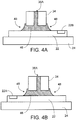
FIG. 4A is a cross-sectional end view of the module taken along line B-B inFIG. 1A after injection of adhesive. -
FIG. 4B is a cross-sectional view of the module taken along line C-C inFIG. 1 after injection of adhesive. -
FIG. 5 is a cross-sectional end view showing various dimensions of the module ofFIG. 1A . -
FIG. 6 is a cross-sectional side view showing further dimensions of the module ofFIG. 1A . -
FIGS. 7A - 7B illustrate injection of adhesive to form part of wall according to some implementations not forming part of the claimed invention. -
FIG. 8A is a top view arrangement of a second example of an optoelectronic module not forming part of the claimed invention. -
FIG. 8B is a cross-sectional side view of the module ofFIG. 8A taken along line E-E. -
FIGS. 9A and 9B show top view arrangements of a third example of an optoelectronic module. -
FIGS. 10A and 10B show further examples of a bridge portion of an internal module wall. -
FIGS. 11 - 13 illustrate methods of fabricating the modules. -
FIG. 14 illustrates pre-cure steps in the method ofFIG. 13 . -
FIGS. 15A - 15L illustrate a wafer-level method of fabricating optoelectronic modules. -
FIG. 16 illustrates an example of an optoelectronic module made by the method ofFIGS. 15A - 15L . -
FIG. 17 is a top view of spacer. -
FIGS. 18A- 18D are cross-sectional side views of the spacer, taken along lines x-x, during different stages of building up a wall on a bridge portion. -
FIGS. 19A - 19C illustrate examples of screens for building up the wall ofFIGS. 18B - 18D . -
FIG. 20 illustrates attachment of a substrate and sensor chip to the spacer ofFIG. 18D . -
FIG. 21 illustrates a top view of the spacer ofFIG. 18D attached to a substrate on which is mounted a sensor chip. - As shown in
FIGS. 1A - 1B , anoptoelectronic module 20 includes an image sensor 22 (e.g., a CCD or CMOS sensor) on a printed circuit board (PCB) orother substrate 24. Theimage sensor 22 is implemented as a contiguous sensor that includes at least twodifferent regions wall 26 separates the module into two distinct chambers oroptical channels image sensor regions light emitter 30 mounted on thesubstrate 24. Thelight emitter 30 can be implemented, for example, as a light emitting diode (LED), infra-red (IR) LED, organic LED (OLED), infra-red (IR) laser or vertical cavity surface emitting lasers (VCSEL), depending on the application. - The pixels in the
region 22A of theimage sensor 22 can be used, for example, to provide reference signals based on light emitted from thelight emitter 30. The pixels in theother region 22B of theimage sensor 22 can be used, for example, to provide detection signals indicative, for example, of light reflected from an object outside the module. Thus, in some implementations, themodule 20 is arranged for proximity sensing. In such applications, light emitted by theemitter 30 is directed toward an object outside themodule 20; a portion of the light reflected by the object may be directed back toward themodule 20 and sensed by the detection pixels in theregion 22B of theimage sensor 22. To prevent optical cross-talk between thechannels wall 26 preferably is substantially light tight and opaque to wavelength(s) of light emitted by thelight emitter 30. Themodule 20 may include processing circuitry to read and process signals from the image sensor. Themodule 20 also may include control circuitry to control turning the emitter on and off. - In the illustrated example, the
wall 26 spans across the width of theimage sensor 22. Eachend 26A of thewall 26 is in contact with aspacer 32 that separates thePCB substrate 24 from anoptics assembly 25 disposed over thechannels spacer 32, which laterally encircles theimage sensor 22 andlight emitter 30, can serve as outer walls of themodule 20. Thespacer 32 can be composed, for example, of a material that is substantially opaque to, or significantly attenuates, light at wavelength(s) emitted by thelight emitter 30. For example, in some cases, thespacer 32 is composed of a flowable polymer material (e.g., epoxy, acrylate, polyurethane, or silicone) containing a non-transparent filler (e.g., carbon black, a pigment, an inorganic filler, or a dye). Theoptics assembly 25 can be implemented, for example, by a lens wafer 27 (e.g., a PCB wafer) that has through-holes filled with transparent material formingtransmissive regions 21 on which, or in which, beam shaping elements such aslenses 23 are formed. - In the implementation of
FIGS. 1A-1B , thewall 26 is composed of several regions. Abridge region 34 extends over theimage sensor 22 and includes one or more adhesive-filledconduits central conduit 36A and two side-edge conduits 36B. Thearea 38 between thebridge region 34 of thewall 26 and the top surface of theimage sensor 22 is filled with adhesive. Likewise, theareas 40 between the side-edges of theimage sensor 22 and the opposing inner edge of thespacer 32 are filled with adhesive. Thebridge region 34 of the wall 26 (other than the adhesive-filledconduits bridge region 34 is formed as a single contiguous unitary piece with thespacer 32. In its hardened (i.e., cured) state, the adhesive in theconduits areas light emitter 30. In this example, thebridge 34, the adhesive-filledconduits areas wall 26. -
FIGS. 2 and3A - 3B illustrate a technique for forming thewall 26. First, as shown inFIG. 2 , a spacer 32 - formed integrally with abridge portion 34 having conduits (i.e., openings) 36A, 36B - is attached to thePCB substrate 24 on which theimage sensor 22 is mounted. Thecentral conduit 36A of thebridge portion 34 can be disposed directly over theimage sensor 22, whereas each of the side-edge conduits 36B can be disposed over aspace 40 that is between a sensor side-edge 42 and an opposinginner edge 44 of thespacer 32. Then, adhesive (e.g., epoxy) 46 is injected into the conduits (i.e.,central conduit 36A as shown in the end views ofFIGS. 3A - 3B , as well as side-edge conduits 36B). As the adhesive 46 flows through thecentral conduit 36A and onto the top of theimage sensor 22, surface forces can prevent the adhesive 46 from flowing onto thesensitive regions image sensor 22. The viscosity and composition of the adhesive 46, as well as the thickness (t) of thespace 38 between the top surface of theimage sensor 22 and the bottom of thebridge portion 34, should be selected to provide appropriate contact angles (α and β) such that the surface forces prevent the adhesive 46 from flowing onto thesensitive regions image sensor 22. The adhesive 46 is allowed to continue to flow until it fills thespaces conduits FIGS. 4A - 4B , the resultingoverflow meniscus 48 should not be so large as to contaminate the sensitive regions of the image sensor 22 (e.g.,regions - In some implementations, a viscosity in the range of 400 - 7,000 (MPa • s) is suitable for the adhesive (i.e., prior to curing). For some implementations, a viscosity in the range of 3,000 - 6,000 (MPa • s) is advantageous. Other values may be suitable for other implementations.
FIGS. 5 and 6 illustrate various dimensions of the module for some implementations. For example, the following values may be suitable in some instances: - bridge width (a): 200 µm - 300 µm (e.g., 250 µm);
- conduit width (b): 80 µm - 120 µm (e.g., 100 µm);
- image sensor height (c): 125 µm - 175 µm (e.g., 150 µm);
- bridge height and conduit height (d): 175 µm - 225 µm (e.g., 200 µm);
- width of overflow meniscus (p): 50 µm - 250 µm;
- width of space between sensor-edge and spacer (s): 100 µm - 300 µm (e.g., 100µm);
- height of the space between top of image sensor and bottom of bridge region (t): 20 µm - 100 µm (e.g., 50 µm).
- After injecting the adhesive 46 into the
conduits - In some implementations not forming part of the claimed invention, instead of injecting adhesive into conduits in the bridge portion of the wall, adhesive 46 is dispensed from the side, for example, in one of the
areas 40 between a side-edge 42 of theimage sensor 22 and aninner edge 44 of thespacer 32, as illustrated byFIG. 7A . The adhesive 46 can be injected, for example, using a jetting technique. Surface forces draw the adhesive 46 over the top of theimage sensor 22 so as to fill the space 38 (seeFIG. 7B ), without too much lateral spreading of the adhesive. In this way, the adhesive 46 can fill thespaces sensitive regions image sensor 22. In this implementation, thebridge portion 34 of thewall 26 does not include conduits for the adhesive. Thus, the width ('a') of thebridge 34 can be made somewhat smaller (e.g., 200 µm) than the corresponding width of the bridge in the example ofFIG. 5 . An example of the resultingmodule 20A is illustrated inFIGS. 8A and 8B . - In some implementations, as shown in
FIG. 9A , it can be advantageous to form abridge 34 havingnarrow portions 34A each of which is opposite asensitive region image sensor 22. Thethinner sections 34A can increase the lateral distance between thesensitive regions image sensor 22 and theoverflow meniscus 48 formed by the adhesive (seeFIG. 9B ). The thickness ('e') of thethinner portions 34A of thebridge 34 should be sufficiently large to ensure mechanical stability (e.g., e ≥ 100 µm). In some instances, the width ('p') of themeniscus 48 is in the range of 50 - 250 µm. These values may differ for some implementations. - In the foregoing examples, the lower edges of the
bridge portion 34 are substantially square. In some cases, however, thebridge portion 34 can have lower edges with cut-out regions 50 (see, e.g.,FIGS. 10A, 10B ). The cut-outregions 50 can allow the top of the overflow meniscus of the adhesive 46 to be drawn upwards. As more of the adhesive 46 is drawn upwards, the lateral spread of the overflow meniscus can be reduced, which can help keep the adhesive 46 away from thesensitive regions image sensor 22. The cut-outregions 50 can have shapes other than those illustrated inFIGS. 10A - 10B . - In the foregoing examples, the sensitive regions of the
image sensor 22 are described as being optically sensitive regions (i.e., pixels) that may be damaged if the adhesive comes into contact with them. However, in some implementations, the sensitive regions may be other regions of theimage sensor 22 that are, or may be, sensitive to contamination by the adhesive. - The foregoing modules can be fabricated various several techniques, examples of which are described in detail below.
- In a first fabrication method, a
spacer 32, including an integratedbridge portion 34, is formed, for example, by replication/paddle dispensing or vacuum injection molding (FIG. 11 , block 102). Next, plasma activation (e.g., O2 and heat) of thespacer 32 and a PCB substrate 24 (with theimage sensor 22 mounted thereon) can be performed to improve wettability of the surfaces (104). Adhesive (e.g., thermally curable epoxy) then is dispensed onto thespacer 32 and/or the PCB substrate 24 (106), and thespacer 32 andPCB substrate 24 are aligned and brought into contact with one another (108). Additional adhesive (e.g., thermally or UV curable epoxy) is provided to fill thespace 30 beneath thebridge portion 34 and theareas 40 between side-edges 42 of theimage sensor 22 andinner edges 44 of the spacer 32 (block 110). Additional adhesive (e.g., thermally curable) is provided on the surface of an optics assembly (116), which is aligned and attached to the spacer/substrate assembly (118). The adhesive(s) then are cured, for example, thermally (120). - A second fabrication method is illustrated by
FIG. 12 . This method is similar to the method ofFIG. 11 , but also includes partially curing the additional adhesive provided inblock 110 to fill thespace 30 beneath thebridge portion 34 and theareas 40 between side-edges 42 of theimage sensor 22 andinner edges 44 of thespacer 32. In this case, the adhesive provided inblock 110 should be a dual-cure adhesive (e.g., requiring both UV and thermal curing to achieve complete curing of the adhesive). The partial flash cure (block 112), which can take place beforeblock 116, can be performed, for example, using UV radiation and can help prevent the components from moving out of alignment during subsequent processing. The curing process can be completed in block 120 (i.e., using a thermal cure). - A third fabrication method is illustrated by
FIG. 13 . This method is similar to the method ofFIG. 12 , but instead of performing a flash cure (block 112) only after providing the adhesive (block 110), the overflow meniscus formed by the adhesive is exposed to UV radiation continuously as the meniscus develops (block 114).FIG. 14 illustrates an example of this pre-cure process (blocks 110 and 114). During the pre-cure process, asUV radiation 52 is directed at theoverflow meniscus 48 as it forms, a curedadhesive shell 46A is formed, which helps prevent the adhesive from reaching thesensitive regions image sensor 22. On the other hand, theuncured adhesive 46B under thebridge portion 34, as well as the adhesive 46C being applied, remains viscous, which allows more adhesive to be drawn under thebridge portion 34 so as to fill the space between the lower surface of thebridge portion 34 and the top surface of theimage sensor 22. The curing process can be completed in block 120 (i.e., using a thermal cure). - Another wafer-level fabrication method is illustrated in
FIGS. 15A - 15L and can be used to manufacture multiple modules such as themodule 200 ofFIG. 16 , which includes an image sensor (e.g., time-of-flight (TOF) sensor) 222, a light emitter (e.g., VCSEL) 230, and an application-specific integrated circuit (ASIC) 227, each of which can be implemented, for example, as a semiconductor integrated chip mounted on a common PCB orother substrate 224. Thesensor 222, thelight emitter 230 and theASIC 227 can be encased (i.e., overmolded), for example, with aclear epoxy 240, which, in some instances, also formsrespective lenses 242 over thesensor 222 and theemitter 230. Themodule housing 225, includingsidewalls 232 and acover 225, as well as aninternal wall 226 separating the module into two distinct chambers oroptical channels wall 226 includes a bridge portion that spans across thesensor 222 such that eachchamber image sensor region sensors 222 can be formed in two epoxy dispensing/injection steps. - As shown in
FIG. 15A , to makemodules 200, a plurality ofimage sensors 222,ASICs 227 andlight emitters 230 are mounted, for example, on aPCB substrate 301. Next, as shown inFIG. 15B , black epoxy is dispensed onto eachTOF chip 222 to form a blackepoxy foundation layer 303 for subsequent formation of the bridge portion of thewall 226. In some implementations, the height of thefoundation layer 303, which can be provided, for example, using a dispensing valve, is about 30-50 µm. After dispensing the black epoxy for thefoundation layer 303, the epoxy is cured thermally and/or by UV radiation. - As illustrated by
FIG. 15C , thePCB substrate 301 is mounted toUV tape 305 and then is situated between a first top tool (i.e., a vacuum chuck/PDMS chuck) 311 and asecond bottom tool 307, and is surrounded by a sealingplate 309 to facilitate further processing. Thetop tool 307 can includefeatures 313 corresponding to the location of lenses. With thetools overmold 315 for thesensors 222, theASICs 227 and theemitters 230. The injected epoxy also formslenses 317 defined by the features 313 (if present). Theclear epoxy 315 then is cured (e.g., by UV radiation and/or heat). Thus, the same injection molding process can be used to form both theovermold 315 and thelenses 317. - Next, the assembly is de-molded by removing the assembly from the
tools plate 309. The resulting assembly is shown inFIG. 15D . TheUV tape 305 then is removed, for example, by applying UV radiation. - As indicated by
FIG. 15E , portions of theclear epoxy 315 are removed (e.g., mechanically) selectively from two different types of regions. In particular, the epoxy 315 is removed substantially fromareas 319 between adjacent groups of thechips areas 319 subsequently are filled in with black epoxy to form outer walls (i.e., spacers) for the modules. Theclear epoxy 315 also is removed selectively fromareas 321 directly above the foundation layers 303. For example, a narrow trench can be machined by dicing directly above thefoundation layer 303 formed over eachsensor chip 222. An advantage of having previously provided thefoundation layer 303 is that it helps prevent the mechanical dicing from cutting into the top of the sensor chips 222. As explained below, thetrenches 321 also subsequently are filled in with black epoxy so to complete the bridge portion of thewall 226 that spans across thesensor chip 222. - As illustrated by
FIG. 15F , thePCB substrate 301 is mounted toUV tape 323 and then is situated between a first top tool (i.e., a PDMS baffle tool) 327 and a second bottom tool (i.e., a PDMS chuck) 325, and is surrounded by a sealingplate 329 to facilitate further processing. With thetools black epoxy 331 is injected (either with or without vacuum). The portions of the injectedblack epoxy 331 that fill thetrenches 321 come into contact with the previously formed foundation layers 303, thereby completing the bridge portion of the wall across the sensor chips 222. As theblack epoxy 331 fills thetrenches 321, it also forms the outer housing (i.e., sidewalls and cover) for the modules. Thetop tool 327 also can include features to seal and protect the lenses during injection of theblack epoxy 331. The epoxy 331 then is cured, for example, thermally and/or by UV radiation. - Next, as indicated by
FIG. 15G , thebottom tool 325 is removed from the assembly, and theUV tape 323 is removed as well. In some cases, with thefirst tool 327 still in place, the entire assembly is flipped over (seeFIG. 15H ), andtrenches 333 are formed (e.g., by laser trenching) through thePCB substrate 301 in areas between adjacent groups of thechips trenches 333 can extend somewhat into theblack epoxy 321. In some cases, thetrenches 333 can help relieve warping that may be present in the PCB/spacer structure. In other cases, thetrenches 333 can enable correction of such warping when the assembly is mounted to another support during subsequent processing. - After forming the
trenches 333, thefirst tool 327 is removed (seeFIG. 15I ), andUV dicing tape 335 is fixed to the same side of the resultingassembly 332 from which thefirst tool 327 was removed (seeFIG. 15J ). Next, the resultingassembly 332 is singulated into individual modules by dicing through theblack epoxy 331 at the location of each of thetrenches 333. The dicing is performed vertically through theblack epoxy 331 until theUV dicing tape 335 is reached, thereby separating theassembly 332 into multiple individual modules 334 (seeFIG. 15K ). Following singulation, theUV dicing tape 335 is removed, and thePCB substrate 301 of eachmodule 334 is attached to high-temperature tape 337 (seeFIG. 15L ). Themodules 334 then are hard-baked (e.g., 120 °C for one hour) so to fully cure theepoxies assembly 332 intoindividual modules 334 preferably should take place before the hard-baking so as to avoid warping, breakage and/or delamination of the various components. Before removing themodules 334 from the high-temperature tape 337, an automated optical inspection can be conducted. After removing the high-temperature tape 335, the result is multiple modules like themodule 200 ofFIG. 16 . - As described above in connection with
FIG. 7A , in some implementations, adhesive (e.g., epoxy) 46 can be injected, for example, using a jetting technique to fill thespace 38 between thebridge portion 34, thespacer 32 andPCB substrate 24. However, jetting techniques typically permit only the use of low viscosity epoxy, which may overflow onto sensitive regions of thesensor 22. Further, in some cases, low viscosity epoxy may make it more challenging to build up the height of the epoxy. To alleviate such issues, a multi-step three-dimensional (3D) printing technique can be used to form a wall, or bridge, that spans across the sensor chip and that separates the module into two chambers. In this case, however, the bridge is formed directly on a spacer, and subsequently a PCB substrate, on which the sensor chip is mounted, is attached to the spacer such that the bridge spans across the sensor chip and separates the module into two chambers. - As illustrated in
FIG. 17 , aspacer 402 defines a frame that hasopenings 404 corresponding to two optical channels for the module. Onesurface 403 of thespacer 402 includes abridge region 406 across its width.FIG. 18A illustrates a cross-sectional side view of the spacer 402 (taken along lines x-x inFIG. 17 ) prior to depositing the epoxy to build up the bridge. As can be seen inFIG. 18A , thebridge region 406 has avalley region 408 andshoulders 410 that form an angle θ. In some instances, the angle θ is about 60°, although other angles may be appropriate for some implementations. As described below, several screens (seeFIGS. 19A, 19B, 19C ) are used in sequence to selectively apply high viscosity epoxy onto thespacer 402 so as to build up the bridge (seeFIGS. 18B, 18C and 18D ). - A first screen 420 (
FIG. 19A ) is placed over thesurface 403 of thespacer 402, and high viscosity epoxy is pushed through theopening 422 in thescreen 420. Theopening 422 is shaped and positioned so that the epoxy 411 is deposited in thevalley region 408 of the spacer (seeFIG. 18B ). Preferably, thefirst screen 420 is designed to prevent overflow of the epoxy 411 onto the sensitive areas of the sensor chip (i.e., when the spacer is attached to a substrate on which the sensor chip is mounted). For example, in a particular implementation, the dimensions of theopening 422 in thefirst screen 420 can be as follows: a = 600 µm; b = 400 µm; c = 250 µm; d = 175 µm. Other dimensions or shapes may be appropriate for other implementations. - Next, the
first screen 420 is removed from thespacer 402, and asecond screen 424 is placed over thesurface 403 of the spacer. Additional high viscosity epoxy is pushed throughopenings 426 in thescreen 424. Theopenings 426 are shaped and positioned such that theadditional epoxy 413 is deposited on theshoulders 410 of the spacer (seeFIG. 18C ). For example, in a particular implementation, the dimensions of theopening 426 in thesecond screen 424 can be as follows: e = 250 µm; f = 300 µm. Other dimensions or shapes may be appropriate for other implementations. - Next, the
second screen 424 is removed from thespacer 402, and athird screen 428 is placed over thesurface 403 of the spacer. Additional high viscosity epoxy is pushed throughopenings 430 in thescreen 428. Thethird screen 428 has manysmall openings 430 that can be uniformly spaced. Additional high viscosity epoxy is pushed through theopenings 430 so thatepoxy 415 is deposited more or less uniformly over theentire surface 403 of the spacer (seeFIG. 18D ). - After deposition of the epoxy 411, 413, 415 (collectively referred to as epoxy 417) on the
spacer 402, the epoxy is cured (e.g., thermally and/or by UV radiation). Once theepoxy 417 is hardened, a PCB orother substrate 24, on which a TOF or otherimage sensor chip 22 is mounted, is attached to the epoxy-side of thespacer 402, as shown inFIG. 20 . The epoxy 417 below thebridge portion 406 of thespacer 402 forms part of a wall that spans across thesensor chip 22. An optics assembly (including lenses) then can be attached over the spacer to complete the module. The internal wall, formed by thebridge portion 406 of thespacer 402 and the epoxy 417 extending over thesensor chip 22, separates the module into two chambers that are optically isolated from one another. Each chamber can contain respective light sensitive portions of thesensor chip 22. - The foregoing fabrication methods can, in some instances, be performed on a wafer-level. Wafer-level processes allow multiple modules to be fabricated at the same time. Generally, a wafer refers to a substantially disk- or plate-like shaped item, its extension in one direction (y-direction or vertical direction) is small with respect to its extension in the other two directions (x- and z- or lateral directions). In some implementations, the diameter of the wafer is between 5 cm and 40 cm, and can be, for example, between 10 cm and 31 cm. The wafer may be cylindrical with a diameter, for example, of 2, 4, 6, 8, or 12 inches, one inch being about 2.54 cm. In some implementations of a wafer level process, there can be provisions for at least ten modules in each lateral direction, and in some cases at least thirty or even fifty or more modules in each lateral direction.
Claims (12)
- An optoelectronic module (20) comprising:a contiguous image sensor (22) including a first region (22A) and a second region (22B);a wall (26) separating the module into first (28A) and second channels (28B), the first region of the image sensor (22) disposed in the first channel, and the second region of the image sensor (22) disposed in the second channel, wherein the wall attenuates light at one or more wavelengths detectable by the image sensor,wherein the wall includes a bridge region (34) that spans across the image sensor between the first (28A) and second channels (28B), the wall further including adhesive (46) that fills an area (38) between the bridge region and an upper surface of the image sensor,characterized in thatthe bridge region has one or more conduits (36) for flow of adhesive into the area between the bridge region and an upper surface of the image sensor, wherein the one or more conduits penetrates through the bridge region and is filled with the adhesive.
- The module of claim 1 wherein adhesive also is present in areas (40) adjacent side-edges of the image sensor.
- The module of any one of the previous claims further including a substrate (24) on which the image sensor is mounted, and including a spacer (32) separating the substrate from an optics assembly (25) over the channels, wherein at least a portion of the bridge region is composed of the same material as the spacer and is formed as a single contiguous unitary piece with the spacer.
- The module of any one of the previous claims wherein the first and second regions of the image sensor are sensitive to contamination by the adhesive, and wherein a portion of the adhesive over the image sensor forms an overflow meniscus (48) that does not reach the first or second regions.
- The module of any one of the previous claims wherein a height of a space between an upper surface of the image sensor and a lower surface of the bridge region is in a range of 20µm - 100 µm and wherein the adhesive in the area between the bridge region and an upper surface of the image sensor has an overflow meniscus (48) having a width in a range of 50 µm 250 µm.
- The module of any one of the previous claims wherein the bridge region has lower edges in contact with the adhesive, the lower edges having cut-out regions (50).
- A method of fabricating an optoelectronic module (20), the method comprising:providing a spacer (32) attached to a substrate (24), a contiguous image sensor (22) being mounted on the substrate, wherein the spacer attenuates light at one or more wavelengths detectable by the image sensor, there being a bridge portion (34) spanning across the image sensor, the bridge portion composed of the same material as the spacer and formed as a single contiguous unitary piece with the spacer;providing an adhesive (46) in a space (38) between the bridge portion and an upper surface of the image sensor, and in spaces (40) between side-edges of the image sensor and opposing inner edges of the spacer; andsubsequently curing the adhesive,wherein the bridge portion has one or more conduits (36) for flow of adhesive into the area between the bridge portion and an upper surface of the image sensor, wherein the one or more conduits penetrates through the bridge portion,wherein providing an adhesive includes injecting the adhesive into the one or more conduits in the bridge portion and filling the one or more conduits with the adhesive.
- The method of claim 7 wherein the adhesive is dual-cure adhesive, the method including:partially curing the adhesive using a first technique; andsubsequently completing curing of the adhesive using a second technique after performing other fabrication steps.
- The method of claim 7 wherein the adhesive is a dual-cure adhesive, the method includingcontinuously pre-curing an overflow meniscus (48), formed by the adhesive, wherein the pre-curing is performed as the adhesive is being provided in the space between the bridge portion and an upper surface of the image sensor; andsubsequently completing curing of the adhesive after performing other fabrication steps.
- The method of any one of claims 7-9 wherein the spacer is attached to the substrate by adhesive, the method further including attaching an optics assembly (25) over the image sensor, and subsequently completing curing of all the adhesives.
- The method of any one of claims 7-9 wherein the adhesive, prior to curing, the adhesive has a viscosity in a range of 400 - 7,000 (MPa • s), optionally a viscosity in range of 3,000 - 6,000 (MPa • s).
- The method of any one of claims 7-11 wherein surface forces prevent the adhesive from flowing onto regions of the image sensor that are sensitive to contamination by adhesive, wherein the surface forces prevent the adhesive from flowing onto light sensitive regions of the image sensor.
Applications Claiming Priority (4)
| Application Number | Priority Date | Filing Date | Title |
|---|---|---|---|
| US201462028893P | 2014-07-25 | 2014-07-25 | |
| US201462053294P | 2014-09-22 | 2014-09-22 | |
| US201562156416P | 2015-05-04 | 2015-05-04 | |
| PCT/SG2015/050224 WO2016013977A1 (en) | 2014-07-25 | 2015-07-22 | Optoelectronic modules including an image sensor having regions optically separated from one another |
Publications (3)
| Publication Number | Publication Date |
|---|---|
| EP3172767A1 EP3172767A1 (en) | 2017-05-31 |
| EP3172767A4 EP3172767A4 (en) | 2018-06-27 |
| EP3172767B1 true EP3172767B1 (en) | 2022-01-05 |
Family
ID=55163393
Family Applications (1)
| Application Number | Title | Priority Date | Filing Date |
|---|---|---|---|
| EP15824918.5A Active EP3172767B1 (en) | 2014-07-25 | 2015-07-22 | Optoelectronic modules including an image sensor having regions optically separated from one another |
Country Status (8)
| Country | Link |
|---|---|
| US (1) | US10199412B2 (en) |
| EP (1) | EP3172767B1 (en) |
| JP (1) | JP6689817B2 (en) |
| KR (1) | KR102455919B1 (en) |
| CN (1) | CN106575660B (en) |
| SG (1) | SG11201700235QA (en) |
| TW (1) | TWI685126B (en) |
| WO (1) | WO2016013977A1 (en) |
Families Citing this family (7)
| Publication number | Priority date | Publication date | Assignee | Title |
|---|---|---|---|---|
| US10886420B2 (en) | 2016-04-08 | 2021-01-05 | Ams Sensors Singapore Pte. Ltd. | Thin optoelectronic modules with apertures and their manufacture |
| US10840396B2 (en) * | 2016-04-15 | 2020-11-17 | Ams Sensors Singapore Pte. Ltd. | Optoelectronic modules with alignment spacers and methods for assembling the same |
| CN107786784B (en) * | 2016-08-29 | 2020-06-30 | 光宝电子(广州)有限公司 | Lens assembly and manufacturing method thereof |
| JP6620176B2 (en) * | 2018-01-29 | 2019-12-11 | アオイ電子株式会社 | Semiconductor device |
| CN112106207A (en) * | 2018-03-07 | 2020-12-18 | ams传感器新加坡私人有限公司 | Optoelectronic module and wafer-level method for producing an optoelectronic module |
| EP3620813A1 (en) * | 2018-09-04 | 2020-03-11 | ams AG | Optical sensor arrangement, device and method of manufacturing an optical sensor arrangement |
| CN111463293B (en) * | 2019-01-17 | 2022-05-17 | 光宝光电(常州)有限公司 | Support structure, optical sensor structure and method for manufacturing optical sensor structure |
Family Cites Families (19)
| Publication number | Priority date | Publication date | Assignee | Title |
|---|---|---|---|---|
| JP3880278B2 (en) | 2000-03-10 | 2007-02-14 | オリンパス株式会社 | Solid-state imaging device and manufacturing method thereof |
| TW513558B (en) | 2000-10-27 | 2002-12-11 | Fuji Electric Co Ltd | Range finder for automatic focusing |
| JP2002350129A (en) * | 2001-05-23 | 2002-12-04 | Canon Inc | Measuring apparatus |
| JP4016275B2 (en) * | 2003-06-25 | 2007-12-05 | 富士電機デバイステクノロジー株式会社 | Ranging device |
| EP1812968B1 (en) * | 2004-08-25 | 2019-01-16 | Callahan Cellular L.L.C. | Apparatus for multiple camera devices and method of operating same |
| JP2007110588A (en) * | 2005-10-17 | 2007-04-26 | Funai Electric Co Ltd | Compound-eye imaging apparatus |
| JP4492533B2 (en) * | 2005-12-27 | 2010-06-30 | 船井電機株式会社 | Compound eye imaging device |
| KR100809277B1 (en) * | 2006-07-05 | 2008-03-03 | 삼성전기주식회사 | Camer module having a array lens |
| JP2010021283A (en) * | 2008-07-09 | 2010-01-28 | Panasonic Corp | Solid state imaging device and manufacturing method thereof |
| TWM363080U (en) * | 2009-01-21 | 2009-08-11 | Pixart Imaging Inc | Packaging structure |
| DE102010041937A1 (en) | 2010-10-04 | 2012-04-05 | Robert Bosch Gmbh | Optical shielding device for separating optical paths |
| JP5857399B2 (en) | 2010-11-12 | 2016-02-10 | ソニー株式会社 | Solid-state imaging device and electronic device |
| EP2659510B1 (en) | 2011-07-19 | 2019-01-09 | Heptagon Micro Optics Pte. Ltd. | Method for manufacturing opto-electronic modules |
| US8492181B2 (en) | 2011-12-22 | 2013-07-23 | Stmicroelectronics Pte Ltd. | Embedded wafer level optical package structure and manufacturing method |
| US8772898B2 (en) | 2012-02-09 | 2014-07-08 | Omnivision Technologies, Inc. | Lateral light shield in backside illuminated imaging sensors |
| US9627572B2 (en) | 2012-04-25 | 2017-04-18 | Kyocera Corporation | Light receiving and emitting element module and sensor device using same |
| CN103839840B (en) | 2012-11-22 | 2016-12-21 | 光宝新加坡有限公司 | The manufacture method of sensor unit |
| US9094593B2 (en) * | 2013-07-30 | 2015-07-28 | Heptagon Micro Optics Pte. Ltd. | Optoelectronic modules that have shielding to reduce light leakage or stray light, and fabrication methods for such modules |
| US9543354B2 (en) | 2013-07-30 | 2017-01-10 | Heptagon Micro Optics Pte. Ltd. | Optoelectronic modules that have shielding to reduce light leakage or stray light, and fabrication methods for such modules |
-
2015
- 2015-07-22 WO PCT/SG2015/050224 patent/WO2016013977A1/en active Application Filing
- 2015-07-22 KR KR1020177005060A patent/KR102455919B1/en active IP Right Grant
- 2015-07-22 US US15/329,112 patent/US10199412B2/en active Active
- 2015-07-22 CN CN201580044781.7A patent/CN106575660B/en active Active
- 2015-07-22 EP EP15824918.5A patent/EP3172767B1/en active Active
- 2015-07-22 SG SG11201700235QA patent/SG11201700235QA/en unknown
- 2015-07-22 JP JP2017503988A patent/JP6689817B2/en active Active
- 2015-07-24 TW TW104124161A patent/TWI685126B/en active
Non-Patent Citations (1)
| Title |
|---|
| None * |
Also Published As
| Publication number | Publication date |
|---|---|
| CN106575660B (en) | 2019-07-09 |
| WO2016013977A1 (en) | 2016-01-28 |
| EP3172767A4 (en) | 2018-06-27 |
| KR20170036020A (en) | 2017-03-31 |
| CN106575660A (en) | 2017-04-19 |
| TWI685126B (en) | 2020-02-11 |
| JP2017523612A (en) | 2017-08-17 |
| JP6689817B2 (en) | 2020-04-28 |
| TW201611319A (en) | 2016-03-16 |
| US20170229505A1 (en) | 2017-08-10 |
| SG11201700235QA (en) | 2017-02-27 |
| KR102455919B1 (en) | 2022-10-17 |
| EP3172767A1 (en) | 2017-05-31 |
| US10199412B2 (en) | 2019-02-05 |
Similar Documents
| Publication | Publication Date | Title |
|---|---|---|
| EP3172767B1 (en) | Optoelectronic modules including an image sensor having regions optically separated from one another | |
| US10199426B2 (en) | Optoelectronic modules that have shielding to reduce light leakage or stray light, and fabrication methods for such modules | |
| US10373996B2 (en) | Optical modules including focal length adjustment and fabrication of the optical modules | |
| TWI661241B (en) | Optical modules including customizable spacers for focal length adjustment and/or reduction of tilt, and fabrication of the optical modules | |
| US10193026B2 (en) | Partial spacers for wafer-level fabricated modules | |
| EP3183745B1 (en) | Fabrication method for optoelectronic modules having a silicon substrate | |
| US20070009223A1 (en) | Micro-optics on optoelectronics | |
| TW201327790A (en) | Wafer-level fabrication of optical devices, in particular of modules for computational cameras | |
| JP2017523612A5 (en) | ||
| EP3374815B1 (en) | Optical element stack assemblies | |
| US20180266877A1 (en) | Optical Devices and Methods of Making Same | |
| TW201626021A (en) | Optical element stack assemblies | |
| EP3341974B1 (en) | Optical assemblies including a spacer adhering directly to a substrate | |
| TWI638465B (en) | Modules having multiple optical channels including optical elements at different heights above the optoelectronic devices |
Legal Events
| Date | Code | Title | Description |
|---|---|---|---|
| STAA | Information on the status of an ep patent application or granted ep patent |
Free format text: STATUS: THE INTERNATIONAL PUBLICATION HAS BEEN MADE |
|
| PUAI | Public reference made under article 153(3) epc to a published international application that has entered the european phase |
Free format text: ORIGINAL CODE: 0009012 |
|
| STAA | Information on the status of an ep patent application or granted ep patent |
Free format text: STATUS: REQUEST FOR EXAMINATION WAS MADE |
|
| 17P | Request for examination filed |
Effective date: 20170127 |
|
| AK | Designated contracting states |
Kind code of ref document: A1 Designated state(s): AL AT BE BG CH CY CZ DE DK EE ES FI FR GB GR HR HU IE IS IT LI LT LU LV MC MK MT NL NO PL PT RO RS SE SI SK SM TR |
|
| AX | Request for extension of the european patent |
Extension state: BA ME |
|
| DAV | Request for validation of the european patent (deleted) | ||
| DAX | Request for extension of the european patent (deleted) | ||
| RIC1 | Information provided on ipc code assigned before grant |
Ipc: H01L 27/146 20060101AFI20180214BHEP Ipc: H01L 31/00 20060101ALI20180214BHEP |
|
| A4 | Supplementary search report drawn up and despatched |
Effective date: 20180528 |
|
| RIC1 | Information provided on ipc code assigned before grant |
Ipc: H01L 27/146 20060101AFI20180522BHEP Ipc: H01L 31/00 20060101ALI20180522BHEP |
|
| STAA | Information on the status of an ep patent application or granted ep patent |
Free format text: STATUS: EXAMINATION IS IN PROGRESS |
|
| 17Q | First examination report despatched |
Effective date: 20201112 |
|
| GRAP | Despatch of communication of intention to grant a patent |
Free format text: ORIGINAL CODE: EPIDOSNIGR1 |
|
| STAA | Information on the status of an ep patent application or granted ep patent |
Free format text: STATUS: GRANT OF PATENT IS INTENDED |
|
| INTG | Intention to grant announced |
Effective date: 20210721 |
|
| GRAS | Grant fee paid |
Free format text: ORIGINAL CODE: EPIDOSNIGR3 |
|
| GRAA | (expected) grant |
Free format text: ORIGINAL CODE: 0009210 |
|
| STAA | Information on the status of an ep patent application or granted ep patent |
Free format text: STATUS: THE PATENT HAS BEEN GRANTED |
|
| AK | Designated contracting states |
Kind code of ref document: B1 Designated state(s): AL AT BE BG CH CY CZ DE DK EE ES FI FR GB GR HR HU IE IS IT LI LT LU LV MC MK MT NL NO PL PT RO RS SE SI SK SM TR |
|
| REG | Reference to a national code |
Ref country code: GB Ref legal event code: FG4D |
|
| REG | Reference to a national code |
Ref country code: CH Ref legal event code: EP |
|
| REG | Reference to a national code |
Ref country code: AT Ref legal event code: REF Ref document number: 1461344 Country of ref document: AT Kind code of ref document: T Effective date: 20220115 |
|
| REG | Reference to a national code |
Ref country code: DE Ref legal event code: R096 Ref document number: 602015076290 Country of ref document: DE |
|
| REG | Reference to a national code |
Ref country code: IE Ref legal event code: FG4D |
|
| REG | Reference to a national code |
Ref country code: LT Ref legal event code: MG9D |
|
| REG | Reference to a national code |
Ref country code: NL Ref legal event code: MP Effective date: 20220105 |
|
| REG | Reference to a national code |
Ref country code: AT Ref legal event code: MK05 Ref document number: 1461344 Country of ref document: AT Kind code of ref document: T Effective date: 20220105 |
|
| PG25 | Lapsed in a contracting state [announced via postgrant information from national office to epo] |
Ref country code: NL Free format text: LAPSE BECAUSE OF FAILURE TO SUBMIT A TRANSLATION OF THE DESCRIPTION OR TO PAY THE FEE WITHIN THE PRESCRIBED TIME-LIMIT Effective date: 20220105 |
|
| PG25 | Lapsed in a contracting state [announced via postgrant information from national office to epo] |
Ref country code: SE Free format text: LAPSE BECAUSE OF FAILURE TO SUBMIT A TRANSLATION OF THE DESCRIPTION OR TO PAY THE FEE WITHIN THE PRESCRIBED TIME-LIMIT Effective date: 20220105 Ref country code: RS Free format text: LAPSE BECAUSE OF FAILURE TO SUBMIT A TRANSLATION OF THE DESCRIPTION OR TO PAY THE FEE WITHIN THE PRESCRIBED TIME-LIMIT Effective date: 20220105 Ref country code: PT Free format text: LAPSE BECAUSE OF FAILURE TO SUBMIT A TRANSLATION OF THE DESCRIPTION OR TO PAY THE FEE WITHIN THE PRESCRIBED TIME-LIMIT Effective date: 20220505 Ref country code: NO Free format text: LAPSE BECAUSE OF FAILURE TO SUBMIT A TRANSLATION OF THE DESCRIPTION OR TO PAY THE FEE WITHIN THE PRESCRIBED TIME-LIMIT Effective date: 20220405 Ref country code: LT Free format text: LAPSE BECAUSE OF FAILURE TO SUBMIT A TRANSLATION OF THE DESCRIPTION OR TO PAY THE FEE WITHIN THE PRESCRIBED TIME-LIMIT Effective date: 20220105 Ref country code: HR Free format text: LAPSE BECAUSE OF FAILURE TO SUBMIT A TRANSLATION OF THE DESCRIPTION OR TO PAY THE FEE WITHIN THE PRESCRIBED TIME-LIMIT Effective date: 20220105 Ref country code: ES Free format text: LAPSE BECAUSE OF FAILURE TO SUBMIT A TRANSLATION OF THE DESCRIPTION OR TO PAY THE FEE WITHIN THE PRESCRIBED TIME-LIMIT Effective date: 20220105 Ref country code: BG Free format text: LAPSE BECAUSE OF FAILURE TO SUBMIT A TRANSLATION OF THE DESCRIPTION OR TO PAY THE FEE WITHIN THE PRESCRIBED TIME-LIMIT Effective date: 20220405 |
|
| PG25 | Lapsed in a contracting state [announced via postgrant information from national office to epo] |
Ref country code: PL Free format text: LAPSE BECAUSE OF FAILURE TO SUBMIT A TRANSLATION OF THE DESCRIPTION OR TO PAY THE FEE WITHIN THE PRESCRIBED TIME-LIMIT Effective date: 20220105 Ref country code: LV Free format text: LAPSE BECAUSE OF FAILURE TO SUBMIT A TRANSLATION OF THE DESCRIPTION OR TO PAY THE FEE WITHIN THE PRESCRIBED TIME-LIMIT Effective date: 20220105 Ref country code: GR Free format text: LAPSE BECAUSE OF FAILURE TO SUBMIT A TRANSLATION OF THE DESCRIPTION OR TO PAY THE FEE WITHIN THE PRESCRIBED TIME-LIMIT Effective date: 20220406 Ref country code: FI Free format text: LAPSE BECAUSE OF FAILURE TO SUBMIT A TRANSLATION OF THE DESCRIPTION OR TO PAY THE FEE WITHIN THE PRESCRIBED TIME-LIMIT Effective date: 20220105 Ref country code: AT Free format text: LAPSE BECAUSE OF FAILURE TO SUBMIT A TRANSLATION OF THE DESCRIPTION OR TO PAY THE FEE WITHIN THE PRESCRIBED TIME-LIMIT Effective date: 20220105 |
|
| PG25 | Lapsed in a contracting state [announced via postgrant information from national office to epo] |
Ref country code: IS Free format text: LAPSE BECAUSE OF FAILURE TO SUBMIT A TRANSLATION OF THE DESCRIPTION OR TO PAY THE FEE WITHIN THE PRESCRIBED TIME-LIMIT Effective date: 20220505 |
|
| REG | Reference to a national code |
Ref country code: DE Ref legal event code: R097 Ref document number: 602015076290 Country of ref document: DE |
|
| PG25 | Lapsed in a contracting state [announced via postgrant information from national office to epo] |
Ref country code: SM Free format text: LAPSE BECAUSE OF FAILURE TO SUBMIT A TRANSLATION OF THE DESCRIPTION OR TO PAY THE FEE WITHIN THE PRESCRIBED TIME-LIMIT Effective date: 20220105 Ref country code: SK Free format text: LAPSE BECAUSE OF FAILURE TO SUBMIT A TRANSLATION OF THE DESCRIPTION OR TO PAY THE FEE WITHIN THE PRESCRIBED TIME-LIMIT Effective date: 20220105 Ref country code: RO Free format text: LAPSE BECAUSE OF FAILURE TO SUBMIT A TRANSLATION OF THE DESCRIPTION OR TO PAY THE FEE WITHIN THE PRESCRIBED TIME-LIMIT Effective date: 20220105 Ref country code: EE Free format text: LAPSE BECAUSE OF FAILURE TO SUBMIT A TRANSLATION OF THE DESCRIPTION OR TO PAY THE FEE WITHIN THE PRESCRIBED TIME-LIMIT Effective date: 20220105 Ref country code: DK Free format text: LAPSE BECAUSE OF FAILURE TO SUBMIT A TRANSLATION OF THE DESCRIPTION OR TO PAY THE FEE WITHIN THE PRESCRIBED TIME-LIMIT Effective date: 20220105 Ref country code: CZ Free format text: LAPSE BECAUSE OF FAILURE TO SUBMIT A TRANSLATION OF THE DESCRIPTION OR TO PAY THE FEE WITHIN THE PRESCRIBED TIME-LIMIT Effective date: 20220105 |
|
| PLBE | No opposition filed within time limit |
Free format text: ORIGINAL CODE: 0009261 |
|
| STAA | Information on the status of an ep patent application or granted ep patent |
Free format text: STATUS: NO OPPOSITION FILED WITHIN TIME LIMIT |
|
| PG25 | Lapsed in a contracting state [announced via postgrant information from national office to epo] |
Ref country code: AL Free format text: LAPSE BECAUSE OF FAILURE TO SUBMIT A TRANSLATION OF THE DESCRIPTION OR TO PAY THE FEE WITHIN THE PRESCRIBED TIME-LIMIT Effective date: 20220105 |
|
| 26N | No opposition filed |
Effective date: 20221006 |
|
| PG25 | Lapsed in a contracting state [announced via postgrant information from national office to epo] |
Ref country code: SI Free format text: LAPSE BECAUSE OF FAILURE TO SUBMIT A TRANSLATION OF THE DESCRIPTION OR TO PAY THE FEE WITHIN THE PRESCRIBED TIME-LIMIT Effective date: 20220105 Ref country code: MC Free format text: LAPSE BECAUSE OF FAILURE TO SUBMIT A TRANSLATION OF THE DESCRIPTION OR TO PAY THE FEE WITHIN THE PRESCRIBED TIME-LIMIT Effective date: 20220105 |
|
| REG | Reference to a national code |
Ref country code: CH Ref legal event code: PL |
|
| GBPC | Gb: european patent ceased through non-payment of renewal fee |
Effective date: 20220722 |
|
| REG | Reference to a national code |
Ref country code: BE Ref legal event code: MM Effective date: 20220731 |
|
| PG25 | Lapsed in a contracting state [announced via postgrant information from national office to epo] |
Ref country code: LU Free format text: LAPSE BECAUSE OF NON-PAYMENT OF DUE FEES Effective date: 20220722 Ref country code: LI Free format text: LAPSE BECAUSE OF NON-PAYMENT OF DUE FEES Effective date: 20220731 Ref country code: CH Free format text: LAPSE BECAUSE OF NON-PAYMENT OF DUE FEES Effective date: 20220731 |
|
| PG25 | Lapsed in a contracting state [announced via postgrant information from national office to epo] |
Ref country code: GB Free format text: LAPSE BECAUSE OF NON-PAYMENT OF DUE FEES Effective date: 20220722 Ref country code: BE Free format text: LAPSE BECAUSE OF NON-PAYMENT OF DUE FEES Effective date: 20220731 |
|
| PG25 | Lapsed in a contracting state [announced via postgrant information from national office to epo] |
Ref country code: IT Free format text: LAPSE BECAUSE OF FAILURE TO SUBMIT A TRANSLATION OF THE DESCRIPTION OR TO PAY THE FEE WITHIN THE PRESCRIBED TIME-LIMIT Effective date: 20220105 Ref country code: IE Free format text: LAPSE BECAUSE OF NON-PAYMENT OF DUE FEES Effective date: 20220722 |
|
| P01 | Opt-out of the competence of the unified patent court (upc) registered |
Effective date: 20230825 |
|
| PGFP | Annual fee paid to national office [announced via postgrant information from national office to epo] |
Ref country code: FR Payment date: 20230726 Year of fee payment: 9 Ref country code: DE Payment date: 20230719 Year of fee payment: 9 |
|
| PG25 | Lapsed in a contracting state [announced via postgrant information from national office to epo] |
Ref country code: HU Free format text: LAPSE BECAUSE OF FAILURE TO SUBMIT A TRANSLATION OF THE DESCRIPTION OR TO PAY THE FEE WITHIN THE PRESCRIBED TIME-LIMIT; INVALID AB INITIO Effective date: 20150722 |