EP3171398A1 - Array substrate and manufacturing method therefor, and display apparatus - Google Patents
Array substrate and manufacturing method therefor, and display apparatus Download PDFInfo
- Publication number
- EP3171398A1 EP3171398A1 EP14861186.6A EP14861186A EP3171398A1 EP 3171398 A1 EP3171398 A1 EP 3171398A1 EP 14861186 A EP14861186 A EP 14861186A EP 3171398 A1 EP3171398 A1 EP 3171398A1
- Authority
- EP
- European Patent Office
- Prior art keywords
- insulating layer
- forming
- electrode
- connection part
- layer
- Prior art date
- Legal status (The legal status is an assumption and is not a legal conclusion. Google has not performed a legal analysis and makes no representation as to the accuracy of the status listed.)
- Withdrawn
Links
Images




Classifications
-
- G—PHYSICS
- G02—OPTICS
- G02F—OPTICAL DEVICES OR ARRANGEMENTS FOR THE CONTROL OF LIGHT BY MODIFICATION OF THE OPTICAL PROPERTIES OF THE MEDIA OF THE ELEMENTS INVOLVED THEREIN; NON-LINEAR OPTICS; FREQUENCY-CHANGING OF LIGHT; OPTICAL LOGIC ELEMENTS; OPTICAL ANALOGUE/DIGITAL CONVERTERS
- G02F1/00—Devices or arrangements for the control of the intensity, colour, phase, polarisation or direction of light arriving from an independent light source, e.g. switching, gating or modulating; Non-linear optics
- G02F1/01—Devices or arrangements for the control of the intensity, colour, phase, polarisation or direction of light arriving from an independent light source, e.g. switching, gating or modulating; Non-linear optics for the control of the intensity, phase, polarisation or colour
- G02F1/13—Devices or arrangements for the control of the intensity, colour, phase, polarisation or direction of light arriving from an independent light source, e.g. switching, gating or modulating; Non-linear optics for the control of the intensity, phase, polarisation or colour based on liquid crystals, e.g. single liquid crystal display cells
- G02F1/133—Constructional arrangements; Operation of liquid crystal cells; Circuit arrangements
- G02F1/136—Liquid crystal cells structurally associated with a semi-conducting layer or substrate, e.g. cells forming part of an integrated circuit
- G02F1/1362—Active matrix addressed cells
- G02F1/136209—Light shielding layers, e.g. black matrix, incorporated in the active matrix substrate, e.g. structurally associated with the switching element
-
- G—PHYSICS
- G02—OPTICS
- G02F—OPTICAL DEVICES OR ARRANGEMENTS FOR THE CONTROL OF LIGHT BY MODIFICATION OF THE OPTICAL PROPERTIES OF THE MEDIA OF THE ELEMENTS INVOLVED THEREIN; NON-LINEAR OPTICS; FREQUENCY-CHANGING OF LIGHT; OPTICAL LOGIC ELEMENTS; OPTICAL ANALOGUE/DIGITAL CONVERTERS
- G02F1/00—Devices or arrangements for the control of the intensity, colour, phase, polarisation or direction of light arriving from an independent light source, e.g. switching, gating or modulating; Non-linear optics
- G02F1/01—Devices or arrangements for the control of the intensity, colour, phase, polarisation or direction of light arriving from an independent light source, e.g. switching, gating or modulating; Non-linear optics for the control of the intensity, phase, polarisation or colour
- G02F1/13—Devices or arrangements for the control of the intensity, colour, phase, polarisation or direction of light arriving from an independent light source, e.g. switching, gating or modulating; Non-linear optics for the control of the intensity, phase, polarisation or colour based on liquid crystals, e.g. single liquid crystal display cells
- G02F1/133—Constructional arrangements; Operation of liquid crystal cells; Circuit arrangements
- G02F1/136—Liquid crystal cells structurally associated with a semi-conducting layer or substrate, e.g. cells forming part of an integrated circuit
- G02F1/1362—Active matrix addressed cells
- G02F1/136227—Through-hole connection of the pixel electrode to the active element through an insulation layer
-
- G—PHYSICS
- G02—OPTICS
- G02F—OPTICAL DEVICES OR ARRANGEMENTS FOR THE CONTROL OF LIGHT BY MODIFICATION OF THE OPTICAL PROPERTIES OF THE MEDIA OF THE ELEMENTS INVOLVED THEREIN; NON-LINEAR OPTICS; FREQUENCY-CHANGING OF LIGHT; OPTICAL LOGIC ELEMENTS; OPTICAL ANALOGUE/DIGITAL CONVERTERS
- G02F1/00—Devices or arrangements for the control of the intensity, colour, phase, polarisation or direction of light arriving from an independent light source, e.g. switching, gating or modulating; Non-linear optics
- G02F1/01—Devices or arrangements for the control of the intensity, colour, phase, polarisation or direction of light arriving from an independent light source, e.g. switching, gating or modulating; Non-linear optics for the control of the intensity, phase, polarisation or colour
- G02F1/13—Devices or arrangements for the control of the intensity, colour, phase, polarisation or direction of light arriving from an independent light source, e.g. switching, gating or modulating; Non-linear optics for the control of the intensity, phase, polarisation or colour based on liquid crystals, e.g. single liquid crystal display cells
- G02F1/133—Constructional arrangements; Operation of liquid crystal cells; Circuit arrangements
- G02F1/136—Liquid crystal cells structurally associated with a semi-conducting layer or substrate, e.g. cells forming part of an integrated circuit
- G02F1/1362—Active matrix addressed cells
- G02F1/1368—Active matrix addressed cells in which the switching element is a three-electrode device
-
- H—ELECTRICITY
- H10—SEMICONDUCTOR DEVICES; ELECTRIC SOLID-STATE DEVICES NOT OTHERWISE PROVIDED FOR
- H10D—INORGANIC ELECTRIC SEMICONDUCTOR DEVICES
- H10D30/00—Field-effect transistors [FET]
- H10D30/60—Insulated-gate field-effect transistors [IGFET]
- H10D30/67—Thin-film transistors [TFT]
- H10D30/6704—Thin-film transistors [TFT] having supplementary regions or layers in the thin films or in the insulated bulk substrates for controlling properties of the device
- H10D30/6723—Thin-film transistors [TFT] having supplementary regions or layers in the thin films or in the insulated bulk substrates for controlling properties of the device having light shields
-
- H—ELECTRICITY
- H10—SEMICONDUCTOR DEVICES; ELECTRIC SOLID-STATE DEVICES NOT OTHERWISE PROVIDED FOR
- H10D—INORGANIC ELECTRIC SEMICONDUCTOR DEVICES
- H10D30/00—Field-effect transistors [FET]
- H10D30/60—Insulated-gate field-effect transistors [IGFET]
- H10D30/67—Thin-film transistors [TFT]
- H10D30/6729—Thin-film transistors [TFT] characterised by the electrodes
- H10D30/673—Thin-film transistors [TFT] characterised by the electrodes characterised by the shapes, relative sizes or dispositions of the gate electrodes
- H10D30/6733—Multi-gate TFTs
-
- H—ELECTRICITY
- H10—SEMICONDUCTOR DEVICES; ELECTRIC SOLID-STATE DEVICES NOT OTHERWISE PROVIDED FOR
- H10D—INORGANIC ELECTRIC SEMICONDUCTOR DEVICES
- H10D86/00—Integrated devices formed in or on insulating or conducting substrates, e.g. formed in silicon-on-insulator [SOI] substrates or on stainless steel or glass substrates
- H10D86/01—Manufacture or treatment
- H10D86/021—Manufacture or treatment of multiple TFTs
- H10D86/0231—Manufacture or treatment of multiple TFTs using masks, e.g. half-tone masks
-
- H—ELECTRICITY
- H10—SEMICONDUCTOR DEVICES; ELECTRIC SOLID-STATE DEVICES NOT OTHERWISE PROVIDED FOR
- H10D—INORGANIC ELECTRIC SEMICONDUCTOR DEVICES
- H10D86/00—Integrated devices formed in or on insulating or conducting substrates, e.g. formed in silicon-on-insulator [SOI] substrates or on stainless steel or glass substrates
- H10D86/40—Integrated devices formed in or on insulating or conducting substrates, e.g. formed in silicon-on-insulator [SOI] substrates or on stainless steel or glass substrates characterised by multiple TFTs
- H10D86/441—Interconnections, e.g. scanning lines
-
- H—ELECTRICITY
- H10—SEMICONDUCTOR DEVICES; ELECTRIC SOLID-STATE DEVICES NOT OTHERWISE PROVIDED FOR
- H10D—INORGANIC ELECTRIC SEMICONDUCTOR DEVICES
- H10D86/00—Integrated devices formed in or on insulating or conducting substrates, e.g. formed in silicon-on-insulator [SOI] substrates or on stainless steel or glass substrates
- H10D86/40—Integrated devices formed in or on insulating or conducting substrates, e.g. formed in silicon-on-insulator [SOI] substrates or on stainless steel or glass substrates characterised by multiple TFTs
- H10D86/481—Integrated devices formed in or on insulating or conducting substrates, e.g. formed in silicon-on-insulator [SOI] substrates or on stainless steel or glass substrates characterised by multiple TFTs integrated with passive devices, e.g. auxiliary capacitors
-
- H—ELECTRICITY
- H10—SEMICONDUCTOR DEVICES; ELECTRIC SOLID-STATE DEVICES NOT OTHERWISE PROVIDED FOR
- H10D—INORGANIC ELECTRIC SEMICONDUCTOR DEVICES
- H10D86/00—Integrated devices formed in or on insulating or conducting substrates, e.g. formed in silicon-on-insulator [SOI] substrates or on stainless steel or glass substrates
- H10D86/40—Integrated devices formed in or on insulating or conducting substrates, e.g. formed in silicon-on-insulator [SOI] substrates or on stainless steel or glass substrates characterised by multiple TFTs
- H10D86/60—Integrated devices formed in or on insulating or conducting substrates, e.g. formed in silicon-on-insulator [SOI] substrates or on stainless steel or glass substrates characterised by multiple TFTs wherein the TFTs are in active matrices
-
- G—PHYSICS
- G02—OPTICS
- G02F—OPTICAL DEVICES OR ARRANGEMENTS FOR THE CONTROL OF LIGHT BY MODIFICATION OF THE OPTICAL PROPERTIES OF THE MEDIA OF THE ELEMENTS INVOLVED THEREIN; NON-LINEAR OPTICS; FREQUENCY-CHANGING OF LIGHT; OPTICAL LOGIC ELEMENTS; OPTICAL ANALOGUE/DIGITAL CONVERTERS
- G02F1/00—Devices or arrangements for the control of the intensity, colour, phase, polarisation or direction of light arriving from an independent light source, e.g. switching, gating or modulating; Non-linear optics
- G02F1/01—Devices or arrangements for the control of the intensity, colour, phase, polarisation or direction of light arriving from an independent light source, e.g. switching, gating or modulating; Non-linear optics for the control of the intensity, phase, polarisation or colour
- G02F1/13—Devices or arrangements for the control of the intensity, colour, phase, polarisation or direction of light arriving from an independent light source, e.g. switching, gating or modulating; Non-linear optics for the control of the intensity, phase, polarisation or colour based on liquid crystals, e.g. single liquid crystal display cells
- G02F1/133—Constructional arrangements; Operation of liquid crystal cells; Circuit arrangements
- G02F1/1333—Constructional arrangements; Manufacturing methods
- G02F1/1343—Electrodes
- G02F1/134309—Electrodes characterised by their geometrical arrangement
- G02F1/134363—Electrodes characterised by their geometrical arrangement for applying an electric field parallel to the substrate, i.e. in-plane switching [IPS]
-
- G—PHYSICS
- G02—OPTICS
- G02F—OPTICAL DEVICES OR ARRANGEMENTS FOR THE CONTROL OF LIGHT BY MODIFICATION OF THE OPTICAL PROPERTIES OF THE MEDIA OF THE ELEMENTS INVOLVED THEREIN; NON-LINEAR OPTICS; FREQUENCY-CHANGING OF LIGHT; OPTICAL LOGIC ELEMENTS; OPTICAL ANALOGUE/DIGITAL CONVERTERS
- G02F1/00—Devices or arrangements for the control of the intensity, colour, phase, polarisation or direction of light arriving from an independent light source, e.g. switching, gating or modulating; Non-linear optics
- G02F1/01—Devices or arrangements for the control of the intensity, colour, phase, polarisation or direction of light arriving from an independent light source, e.g. switching, gating or modulating; Non-linear optics for the control of the intensity, phase, polarisation or colour
- G02F1/13—Devices or arrangements for the control of the intensity, colour, phase, polarisation or direction of light arriving from an independent light source, e.g. switching, gating or modulating; Non-linear optics for the control of the intensity, phase, polarisation or colour based on liquid crystals, e.g. single liquid crystal display cells
- G02F1/133—Constructional arrangements; Operation of liquid crystal cells; Circuit arrangements
- G02F1/1333—Constructional arrangements; Manufacturing methods
- G02F1/1343—Electrodes
- G02F1/134309—Electrodes characterised by their geometrical arrangement
- G02F1/134372—Electrodes characterised by their geometrical arrangement for fringe field switching [FFS] where the common electrode is not patterned
-
- G—PHYSICS
- G02—OPTICS
- G02F—OPTICAL DEVICES OR ARRANGEMENTS FOR THE CONTROL OF LIGHT BY MODIFICATION OF THE OPTICAL PROPERTIES OF THE MEDIA OF THE ELEMENTS INVOLVED THEREIN; NON-LINEAR OPTICS; FREQUENCY-CHANGING OF LIGHT; OPTICAL LOGIC ELEMENTS; OPTICAL ANALOGUE/DIGITAL CONVERTERS
- G02F1/00—Devices or arrangements for the control of the intensity, colour, phase, polarisation or direction of light arriving from an independent light source, e.g. switching, gating or modulating; Non-linear optics
- G02F1/01—Devices or arrangements for the control of the intensity, colour, phase, polarisation or direction of light arriving from an independent light source, e.g. switching, gating or modulating; Non-linear optics for the control of the intensity, phase, polarisation or colour
- G02F1/13—Devices or arrangements for the control of the intensity, colour, phase, polarisation or direction of light arriving from an independent light source, e.g. switching, gating or modulating; Non-linear optics for the control of the intensity, phase, polarisation or colour based on liquid crystals, e.g. single liquid crystal display cells
- G02F1/133—Constructional arrangements; Operation of liquid crystal cells; Circuit arrangements
- G02F1/136—Liquid crystal cells structurally associated with a semi-conducting layer or substrate, e.g. cells forming part of an integrated circuit
- G02F1/1362—Active matrix addressed cells
- G02F1/136218—Shield electrodes
-
- G—PHYSICS
- G02—OPTICS
- G02F—OPTICAL DEVICES OR ARRANGEMENTS FOR THE CONTROL OF LIGHT BY MODIFICATION OF THE OPTICAL PROPERTIES OF THE MEDIA OF THE ELEMENTS INVOLVED THEREIN; NON-LINEAR OPTICS; FREQUENCY-CHANGING OF LIGHT; OPTICAL LOGIC ELEMENTS; OPTICAL ANALOGUE/DIGITAL CONVERTERS
- G02F1/00—Devices or arrangements for the control of the intensity, colour, phase, polarisation or direction of light arriving from an independent light source, e.g. switching, gating or modulating; Non-linear optics
- G02F1/01—Devices or arrangements for the control of the intensity, colour, phase, polarisation or direction of light arriving from an independent light source, e.g. switching, gating or modulating; Non-linear optics for the control of the intensity, phase, polarisation or colour
- G02F1/13—Devices or arrangements for the control of the intensity, colour, phase, polarisation or direction of light arriving from an independent light source, e.g. switching, gating or modulating; Non-linear optics for the control of the intensity, phase, polarisation or colour based on liquid crystals, e.g. single liquid crystal display cells
- G02F1/133—Constructional arrangements; Operation of liquid crystal cells; Circuit arrangements
- G02F1/136—Liquid crystal cells structurally associated with a semi-conducting layer or substrate, e.g. cells forming part of an integrated circuit
- G02F1/1362—Active matrix addressed cells
- G02F1/1368—Active matrix addressed cells in which the switching element is a three-electrode device
- G02F1/13685—Top gates
Definitions
- the present disclosure relates to the field of display technology, and particularly to an array substrate, a method for fabricating the same, and a display device.
- LTPS low temperature poly-crystalline silicon
- a LTPS thin film transistor array substrate in the prior art mainly comprises: a substrate 01, a buffer layer 02, an active layer 03, a gate electrode 06, a source electrode 05, a drain electrode 04, a common electrode 07, a pixel electrode 08, a gate insulating layer 09, an intermediate dielectric layer 10, a planarization layer 11, and a passivation layer 12.
- a metal shielding layer 13 is further arranged between the buffer layer 02 and the active layer 03 to avoid light from being incident on the active layer 03.
- a storage capacitor is formed between the metal shielding layer 13 under the buffer layer 02 and the active layer 03 to increase storage capacitance.
- the metal shielding layer 13 should be electrically connected with the common electrode 07 by means of a first connection part 14 on the gate insulating layer 09 and a second connection part 15 on the intermediate dielectric layer 10.
- the first connection part 14 is electrically connected with the metal shielding layer 13 by means of a via penetrating the gate insulating layer 09 and the buffer layer 02
- the connection part 15 is electrically connected with the first connection part 14 by means of a via penetrating the intermediate dielectric layer 10
- the common electrode 07 is electrically connected with the second connection part 15 by means of a via penetrating planarization layer 11.
- a storage capacitor can be formed by means of the metal shielding layer and the active layer.
- the metal shielding layer 13 is electrically connected with the common electrode 07 to form the storage capacitor by the metal shielding layer 13 and the active layer 03
- an additional mask process is needed to form a via penetrating the gate insulating layer 09 and the buffer layer 02, so that the first connection part 14, which is used for electrically connecting the common electrode 07 and the metal shielding layer 13, is electrically connected with the metal shielding layer 13 by means of the via.
- the process for fabricating the above-mentioned LTPS thin film transistor array substrate is complicated in flow, high in cost, and long in duration.
- the present disclosure provides an array substrate, a method for fabricating the same, and a display device, which can solve or at least partially alleviate one or more problems in the prior art.
- the present disclosure provides an array substrate, comprising a substrate, and a metal shielding layer, a buffer layer, a top-gate thin film transistor, and a common electrode which are arranged on the substrate successively; wherein in the top-gate thin film transistor, a source/drain electrode is arranged over an active layer and is electrically connected with the active layer by means of a first via penetrating a first insulating layer between the source/drain electrode and the active layer, wherein the array substrate further comprises:
- the metal shielding layer is electrically connected with the common electrode.
- the first connection part used for electrically connecting the metal shielding layer and the common electrode is arranged in the same layer as the source/drain electrode, and is electrically connected with the metal shielding electrode by means of a via penetrating the first insulating layer and the buffer layer.
- the present array substrate can form a storage capacitor between the active layer and the metal shielding layer, thus increasing capacitance of the array substrate.
- the first connection part and the source/drain electrode which are arranged in the same layer can be formed by performing a patterning process for one time, thus reducing the fabricating flow, simplifying the fabricating process, saving the fabricating cost, and decreasing the fabricating time.
- the present array substrate can further comprise a second insulating layer which is arranged between the source/drain electrode and the common electrode, wherein the common electrode is electrically connected with the first connection part by means of a third via penetrating the second insulating layer.
- the present array substrate can further comprise: a pixel electrode which is arranged over the common electrode, a third insulating layer which is arranged between the pixel electrode and the common electrode, and a second connection part which is arranged in the same layer as the common electrode and is used for electrically connecting the pixel electrode and a drain electrode of the source/drain electrode, wherein the second connection part is electrically connected with a drain electrode of the source/drain electrode by means of a fourth via penetrating the second insulating layer, and the pixel electrode is electrically connected with the second connection part by means of a fifth via penetrating the third insulating layer.
- the present array substrate can further comprise: a pixel electrode which is arranged between the source/drain electrode and the common electrode and is insulated from the common electrode, and a second insulating layer which is arranged between the pixel electrode and the source/drain electrode, wherein the pixel electrode is electrically connected with a drain electrode of the source/drain electrode by means of a sixth via penetrating the second insulating layer.
- the present array substrate can further comprise: a third insulating layer which is arranged between the pixel electrode and the common electrode, and a third connection part which is arranged in the same layer as the pixel electrode and is used for electrically connecting the common electrode and the first connection part, wherein the third connection part is electrically connected with the first connection part by means of a seventh via penetrating the second insulating layer, and the common electrode is electrically connected with the third connection part by means of an eighth via penetrating the third insulating layer.
- the present disclosure provides a display device which comprises any one of the array substrate as mentioned above.
- the present disclosure provides a method for fabricating an array substrate, comprising forming an a substrate successively patterns of a metal shielding layer, a buffer layer, a top-gate thin film transistor, and a common electrode; wherein in the top-gate thin film transistor, a source/drain electrode is arranged over an active layer and is electrically connected with the active layer by means of a first via penetrating a first insulating layer between the source/drain electrode and the active layer, wherein the method further comprises:
- the second via penetrating the first insulating layer and the buffer layer is formed by means of a half tone mask plate or a gray tone mask plate.
- the pattern of the first connection part which is used for electrically connecting the metal shielding layer and the common electrode and is electrically connected with the metal shielding layer by means of the second via, is formed by performing a patterning process for one time.
- the present method can reduce the fabricating flow, simplify the fabricating process, save the fabricating cost, and decrease the fabricating time.
- the present method can further comprise:
- the present method can further comprise:
- the present method can further comprise:
- the present method can further comprise:
- An array substrate of the present disclosure as shown in Fig. 3a, Fig. 3b , and Fig. 4 (a top view of the array substrate shown in Fig. 3a ), comprises a substrate 100, and a metal shielding layer 200, a buffer layer 300, a top-gate thin film transistor, and a common electrode 500 which are arranged on the substrate 100 successively.
- a source/drain electrode 410 of the top-gate thin film transistor is arranged over an active layer 420, and is electrically connected with the active layer 420 by means of a first via V1 penetrating a first insulating layer 610 between the source/drain electrode 410 and the active layer 420.
- the array substrate further comprises a first connection part 510, which is arranged in the same layer as the source/drain electrode 410, is used for electrically connecting the metal shielding layer 200 and the common electrode 500, and is electrically connected with the metal shielding layer 200 by means of a second via V2 penetrating the first insulating layer 610 and the buffer layer 300.
- a first connection part 510 which is arranged in the same layer as the source/drain electrode 410, is used for electrically connecting the metal shielding layer 200 and the common electrode 500, and is electrically connected with the metal shielding layer 200 by means of a second via V2 penetrating the first insulating layer 610 and the buffer layer 300.
- the metal shielding layer is electrically connected with the common electrode.
- the first connection part used for electrically connecting the metal shielding layer and the common electrode is arranged in the same layer as the source/drain electrode, and is electrically connected with the metal shielding electrode by means of a via penetrating the first insulating layer and the buffer layer.
- the present array substrate can form a storage capacitor between the active layer and the metal shielding layer, thus increasing capacitance of the array substrate.
- the first connection part and the source/drain electrode which are arranged in the same layer can be formed by performing a patterning process for one time, thus reducing the fabricating flow, simplifying the fabricating process, saving the fabricating cost, and decreasing the fabricating time.
- an orthographic projection of the metal shielding layer 200 onto the substrate 100 at least partially overlaps an orthographic projection of the active layer 420 onto the substrate 100, so that a storage capacitor is formed between the active layer 420 and the metal shielding layer 200.
- the active layer can be made from LTPS or oxide, and the present disclosure is not limited in this aspect.
- Fig. 3a and Fig. 3b there can be only one gate electrode.
- the purpose of providing two gate electrodes 430 is to reduce leakage current of the thin film transistor.
- the active layer 420 may comprise heavily doped regions 421 and lightly doped regions 422.
- the heavily doped regions 421 are arranged in the active layer 420 at regions corresponding to the source/drain electrode 410, for reducing contact resistance between the source/drain electrode 410 and the active layer 420.
- the lightly doped regions 422 are provided between the heavily doped regions 421, and arranged at both sides of the regions corresponding to two gate electrodes 430 in the active layer 420.
- the lightly doped regions 422 can reduce the leakage current in the thin film transistor.
- the arrangement of heavily doped regions 421 and lightly doped regions 422 as shown is only an example. In practice, in some thin film transistors, there is no heavily doped region or lightly doped region. Alternatively, there are more heavily doped regions or lightly doped regions which are arranged at different positions as required.
- the gate electrode in the top-gate thin film transistor, can be arranged over the source/drain electrode, or below the source/drain electrode.
- the gate electrode lies below the source/drain electrode.
- the first insulating layer 610 between the source/drain electrode 410 and the active layer 420 refers to a gate insulating layer 611 between the active layer 420 and a gate electrode 430 and an interlayer dielectric layer 612 between the gate electrode 430 and the source/drain electrode 410.
- the present disclosure is not limited in this aspect.
- the present array substrate as shown in Fig. 3a , further comprises a second insulating layer 620 between the source/drain electrode 410 and the common electrode 500, wherein the common electrode 500 is electrically connected with the first connection part 510 by means of a third via V3 penetrating the second insulating layer 620.
- the present array substrate as shown in Fig. 3a can further comprise: a pixel electrode 700 which is arranged over the common electrode 500, a third insulating layer 630 which is arranged between the pixel electrode 700 and the common electrode 500, and a second connection part 710 which is arranged in the same layer as the common electrode 500 and is used for electrically connecting the pixel electrode 700 and a drain electrode in the source/drain electrode 410.
- the second connection part 710 is electrically connected with a drain electrode in the source/drain electrode 410 by means of a fourth via V4 penetrating the second insulating layer 620, and the pixel electrode 700 is electrically connected with the second connection part 710 by means of a fifth via V5 penetrating the third insulating layer 630.
- the pixel electrode in case the pixel electrode is arranged over the common electrode, the pixel electrode can have a slit shape, the pixel electrode can be made from a transparent conductive material like indium tin oxide, the common electrode can have a plate shape or slit shape, and the common electrode can be made from a transparent conductive material like indium tin oxide.
- the array substrate can further comprise: the pixel electrode 700 which is arranged between the source/drain electrode 410 and the common electrode 500 and is insulated from the common electrode 500, and the second insulating layer 620 which is arranged between the pixel electrode 700 and the source/drain electrode 410.
- the pixel electrode 700 is electrically connected with the drain electrode in the source/drain electrode 410 by means of a sixth via V6 penetrating the second insulating layer 620.
- the array substrate can further comprise: the third insulating layer 630 which is arranged between the pixel electrode 700 and the common electrode 500, and a third connection part 520 which is arranged in the same layer as the pixel electrode 700 and is used for electrically connecting the common electrode 500 and the first connection part 510.
- the third connection part 520 is electrically connected with the first connection part 510 by means of a seventh via V7 penetrating the second insulating layer 620.
- the common electrode 500 is electrically connected with the third connection part 520 by means of an eighth via V8 penetrating the third insulating layer 630.
- the common electrode in case the common electrode is arranged over the pixel electrode, the common electrode can have a slit shape, the common electrode can be made from a transparent conductive material like indium tin oxide, the pixel electrode can have a plate shape or slit shape, and the pixel electrode can be made from a transparent conductive material like indium tin oxide.
- the present array substrate is described in case the top-gate TFT has an active layer of poly-crystalline silicon.
- the present disclosure is also applicable to a top-gate TFT has an active layer of amorphous silicon.
- the present disclosure further provides a display device which comprises the array substrate as described above.
- the display device can be any product or component with a display function, such as a mobile phone, a tablet computer, a television, a monitor, a notebook computer, a digital photo frame, and a navigator. It will be appreciated by the skilled in the art that the display device may comprise other essential components. Thus, these components are not described in detail herein for simplicity, and do not limit the present disclosure in any way.
- the display device can be implemented in a manner similar with the array substrate as mentioned above.
- the present disclosure further provides a method for fabricating an array substrate, comprising forming an a substrate successively patterns of a metal shielding layer, a buffer layer, a top-gate thin film transistor, and a common electrode; wherein in the top-gate thin film transistor, a source/drain electrode is arranged over an active layer and is electrically connected with the active layer by means of a first via penetrating a first insulating layer between the source/drain electrode and the active layer, wherein the method further comprises:
- the second via penetrating the first insulating layer and the buffer layer is formed by means of a half tone mask plate or a gray tone mask plate.
- the pattern of the first connection part which is used for electrically connecting the metal shielding layer and the common electrode and is electrically connected with the metal shielding layer by means of the second via, is formed by performing a patterning process for one time.
- the present method can reduce the fabricating flow, simplify the fabricating process, save the fabricating cost, and decrease the fabricating time.
- the patterning process can only comprise photolithographic process.
- the patterning process can comprise photolithographic process and etching steps.
- the patterning process can further comprise a process for forming a predefined pattern, like printing, ink-jetting.
- the photolithographic process refers to a process which comprises forming a film, exposing, developing and forms the pattern by means of photoresist, mask plate, exposure machine.
- a patterning process can be selected according to the structure to be formed in the present disclosure.
- the present method can further comprise: forming a thin film for a second insulating layer between the source/drain electrode and the common electrode to be formed; and forming a third via penetrating the thin film of the second insulating layer by performing a patterning process, wherein the common electrode is electrically connected with the first connection part by means of the third via.
- the present method can further comprise: at the same time as forming the third via, forming, by performing a patterning process for one time, a fourth via penetrating the second insulating layer; at the same time as forming the pattern of the common electrode, forming, by performing a patterning process for one time, a pattern of a second connection part which is used for electrically connecting a pixel electrode to be formed and a drain electrode in the source/drain electrode, wherein the second connection part is electrically connected with the drain electrode by means of the fourth via; after forming the pattern of the common electrode, the method further comprises: forming a thin film of a third insulating layer on the common electrode; forming a fifth via penetrating the thin film of the third insulating layer by performing a patterning process; and forming a pattern of the pixel electrode on the third insulating layer, wherein the pixel electrode is electrically connected with the second connection part by means of the fifth via
- the present method can further comprise: forming a thin film for a second insulating layer between the source/drain electrode and the common electrode to be formed; forming, by performing a patterning process, a sixth via penetrating the thin film of the second insulating layer; and forming a pattern of a pixel electrode on the thin film of the second insulating layer in which the sixth via has been formed, wherein the pixel electrode is electrically connected with a drain electrode in the source/drain electrode by means of the sixth via.
- the present method can further comprise: at the same time as forming the sixth via, forming, by performing a patterning process for one time, a seventh via penetrating the second insulating layer; and at the same time as forming the pattern of the pixel electrode, forming, by performing a patterning process for one time, a pattern of a third connection part which is used for electrically connecting the common electrode to be formed and the first connection part, wherein the third connection part is electrically connected with the first connection part by means of the seventh via; after forming the pattern of the pixel electrode, the method further comprises: forming a thin film of a third insulating layer between the pixel electrode and the common electrode to be formed; and forming, by performing a patterning process, an eighth via penetrating the thin film of the third insulating layer, wherein the common electrode to be formed is electrically connected with the third connection part by means of the eighth via.
- top-gate LTPS TFT with two gates. It will be appreciated that the present disclosure is also applicable to amorphous silicon TFT or oxide TFT which has a single gate and of the top-gate type. All solutions which can increase the storage capacitance of the array substrate by increasing a confronting area between the active layer and the metal shielding layer fall within the scope of the present disclosure.
- the pixel electrode 700 in the array substrate is arranged over the common electrode 500.
- the process for fabricating the array substrate may comprise the following steps.
- the pixel electrode can have a slit shape
- the pixel electrode can be made from a transparent conductive material like indium tin oxide
- the pixel electrode is electrically connected with the second connection part by means of the fifth via.
- the array substrate of the present disclosure is obtained.
- a structural view of the resultant array substrate is shown in Fig. 3a .
- the fabricating process of the array substrate further comprises the following steps.
- the common electrode can have a slit shape
- the common electrode can be made from a transparent conductive material like indium tin oxide
- the common electrode is electrically connected with the third connection part by means of the eighth via.
- the array substrate of the present disclosure is obtained.
- a structural view of the resultant array substrate is shown in Fig. 3b .
- the present disclosure provides an array substrate, a method for fabricating the same, and a display device.
- the metal shielding layer is electrically connected with the common electrode.
- the first connection part used for electrically connecting the metal shielding layer and the common electrode is arranged in the same layer as the source/drain electrode, and is electrically connected with the metal shielding electrode by means of a via penetrating the first insulating layer and the buffer layer. In this manner, the present array substrate can form a storage capacitor between the active layer and the metal shielding layer, thus increasing capacitance of the array substrate.
- the first connection part and the source/drain electrode which are arranged in the same layer can be formed by performing a patterning process for one time, thus reducing the fabricating flow, simplifying the fabricating process, saving the fabricating cost, and decreasing the fabricating time.
Landscapes
- Physics & Mathematics (AREA)
- Nonlinear Science (AREA)
- Engineering & Computer Science (AREA)
- Microelectronics & Electronic Packaging (AREA)
- Mathematical Physics (AREA)
- Chemical & Material Sciences (AREA)
- Crystallography & Structural Chemistry (AREA)
- General Physics & Mathematics (AREA)
- Optics & Photonics (AREA)
- Liquid Crystal (AREA)
- Thin Film Transistor (AREA)
- Devices For Indicating Variable Information By Combining Individual Elements (AREA)
Abstract
Description
- The present application claims the benefit of Chinese Patent Application No.
201410232647.7, filed May 28, 2014 - The present disclosure relates to the field of display technology, and particularly to an array substrate, a method for fabricating the same, and a display device.
- Inherent drawbacks of amorphous silicon lead to a device with low on-state current, low mobility, and poor stability, and thus is hindered from being applied in several fields. LTPS (low temperature poly-crystalline silicon) has emerged to overcome inherent drawbacks of amorphous silicon and thus increase the application field.
- With the development of Thin Film Transistor Liquid Crystal Display (TFT-LCD) technology, LTPS-based display technology has gradually become mainstream. As shown in
Fig. 1 and Fig. 2 , a LTPS thin film transistor array substrate in the prior art mainly comprises: asubstrate 01, abuffer layer 02, anactive layer 03, agate electrode 06, asource electrode 05, adrain electrode 04, acommon electrode 07, apixel electrode 08, agate insulating layer 09, an intermediatedielectric layer 10, aplanarization layer 11, and apassivation layer 12. In an array substrate with a top-gate thin film transistor, as shown inFig. 2 , in order to prevent light from being incident on theactive layer 03 and thus affecting the performance of the thin film transistor, ametal shielding layer 13 is further arranged between thebuffer layer 02 and theactive layer 03 to avoid light from being incident on theactive layer 03. - As required by development of the pixel technology, an important issue is how to increase storage capacitance. In order to increase storage capacitance in the prior art, as shown in
Fig. 2 , in an array substrate with a top-gate thin film transistor, a storage capacitor is formed between themetal shielding layer 13 under thebuffer layer 02 and theactive layer 03 to increase storage capacitance. In particular, in order to apply a common electrode signal to themetal shielding layer 13, themetal shielding layer 13 should be electrically connected with thecommon electrode 07 by means of afirst connection part 14 on thegate insulating layer 09 and asecond connection part 15 on the intermediatedielectric layer 10. Thefirst connection part 14 is electrically connected with themetal shielding layer 13 by means of a via penetrating thegate insulating layer 09 and thebuffer layer 02, theconnection part 15 is electrically connected with thefirst connection part 14 by means of a via penetrating the intermediatedielectric layer 10, and thecommon electrode 07 is electrically connected with thesecond connection part 15 by means of a via penetratingplanarization layer 11. - In the above-mentioned LTPS thin film transistor array substrate, a storage capacitor can be formed by means of the metal shielding layer and the active layer. However, for the purpose that the
metal shielding layer 13 is electrically connected with thecommon electrode 07 to form the storage capacitor by themetal shielding layer 13 and theactive layer 03, an additional mask process is needed to form a via penetrating thegate insulating layer 09 and thebuffer layer 02, so that thefirst connection part 14, which is used for electrically connecting thecommon electrode 07 and themetal shielding layer 13, is electrically connected with themetal shielding layer 13 by means of the via. As a result, the process for fabricating the above-mentioned LTPS thin film transistor array substrate is complicated in flow, high in cost, and long in duration. - The present disclosure provides an array substrate, a method for fabricating the same, and a display device, which can solve or at least partially alleviate one or more problems in the prior art.
- The present disclosure provides an array substrate, comprising a substrate, and a metal shielding layer, a buffer layer, a top-gate thin film transistor, and a common electrode which are arranged on the substrate successively; wherein in the top-gate thin film transistor, a source/drain electrode is arranged over an active layer and is electrically connected with the active layer by means of a first via penetrating a first insulating layer between the source/drain electrode and the active layer, wherein the array substrate further comprises:
- a first connection part which is arranged in the same layer as the source/drain electrode, is used for electrically connecting the metal shielding layer and the common electrode, and is electrically connected with the metal shielding layer by means of a second via penetrating the first insulating layer and the buffer layer.
- In the above array substrate of the present disclosure, the metal shielding layer is electrically connected with the common electrode. Besides, the first connection part used for electrically connecting the metal shielding layer and the common electrode is arranged in the same layer as the source/drain electrode, and is electrically connected with the metal shielding electrode by means of a via penetrating the first insulating layer and the buffer layer. In this manner, the present array substrate can form a storage capacitor between the active layer and the metal shielding layer, thus increasing capacitance of the array substrate. In addition, the first connection part and the source/drain electrode which are arranged in the same layer can be formed by performing a patterning process for one time, thus reducing the fabricating flow, simplifying the fabricating process, saving the fabricating cost, and decreasing the fabricating time.
- For purpose of facilitating implementation, the present array substrate can further comprise a second insulating layer which is arranged between the source/drain electrode and the common electrode, wherein the common electrode is electrically connected with the first connection part by means of a third via penetrating the second insulating layer.
- For purpose of facilitating implementation, the present array substrate can further comprise: a pixel electrode which is arranged over the common electrode, a third insulating layer which is arranged between the pixel electrode and the common electrode, and a second connection part which is arranged in the same layer as the common electrode and is used for electrically connecting the pixel electrode and a drain electrode of the source/drain electrode,
wherein the second connection part is electrically connected with a drain electrode of the source/drain electrode by means of a fourth via penetrating the second insulating layer, and the pixel electrode is electrically connected with the second connection part by means of a fifth via penetrating the third insulating layer. - For purpose of facilitating implementation, the present array substrate can further comprise: a pixel electrode which is arranged between the source/drain electrode and the common electrode and is insulated from the common electrode, and a second insulating layer which is arranged between the pixel electrode and the source/drain electrode,
wherein the pixel electrode is electrically connected with a drain electrode of the source/drain electrode by means of a sixth via penetrating the second insulating layer. - For purpose of facilitating implementation, the present array substrate can further comprise: a third insulating layer which is arranged between the pixel electrode and the common electrode, and a third connection part which is arranged in the same layer as the pixel electrode and is used for electrically connecting the common electrode and the first connection part,
wherein the third connection part is electrically connected with the first connection part by means of a seventh via penetrating the second insulating layer, and the common electrode is electrically connected with the third connection part by means of an eighth via penetrating the third insulating layer. - The present disclosure provides a display device which comprises any one of the array substrate as mentioned above.
- The present disclosure provides a method for fabricating an array substrate, comprising forming an a substrate successively patterns of a metal shielding layer, a buffer layer, a top-gate thin film transistor, and a common electrode; wherein in the top-gate thin film transistor, a source/drain electrode is arranged over an active layer and is electrically connected with the active layer by means of a first via penetrating a first insulating layer between the source/drain electrode and the active layer, wherein the method further comprises:
- at the same time as forming the first via penetrating the first insulating layer, forming a second via penetrating the first insulating layer and the buffer layer by means of a half tone mask plate or a gray tone mask plate; and
- at the same time as forming a pattern of the source/drain electrode, forming, by performing a patterning process for one time, a pattern of a first connection part which is used for electrically connecting the metal shielding layer and the common electrode and is electrically connected with the metal shielding layer by means of the second via.
- In the above mentioned method, at the same time as forming the first via penetrating the first insulating layer, the second via penetrating the first insulating layer and the buffer layer is formed by means of a half tone mask plate or a gray tone mask plate. At the same time as forming the pattern of the source/drain electrode, the pattern of the first connection part, which is used for electrically connecting the metal shielding layer and the common electrode and is electrically connected with the metal shielding layer by means of the second via, is formed by performing a patterning process for one time. Therefore, as compared with the prior art in which the metal shielding layer and the common electrode are electrically connected with each other by means of a first connection part and a second connection part on the first connection part, a mask process which separately forms a via for electrically connecting a first connection part and a metal shielding layer can be omitted in the present method. Therefore, the present method can reduce the fabricating flow, simplify the fabricating process, save the fabricating cost, and decrease the fabricating time.
- For purpose of facilitating implementation, after forming the pattern of the source/drain electrode, and before forming the pattern of the common electrode, the present method can further comprise:
- forming a thin film for a second insulating layer between the source/drain electrode and the common electrode to be formed; and
- forming a third via penetrating the thin film of the second insulating layer by performing a patterning process, wherein the common electrode is electrically connected with the first connection part by means of the third via.
- To simplify the fabricating process, save the fabricating cost, and decrease the production cycle, the present method can further comprise:
- at the same time as forming the third via, forming, by performing a patterning process for one time, a fourth via penetrating the second insulating layer;
- at the same time as forming the pattern of the common electrode, forming, by performing a patterning process for one time, a pattern of a second connection part which is used for electrically connecting a pixel electrode to be formed and a drain electrode in the source/drain electrode, wherein the second connection part is electrically connected with the drain electrode by means of the fourth via;
- after forming the pattern of the common electrode, the method further comprises:
- forming a thin film of a third insulating layer on the common electrode;
- forming a fifth via penetrating the thin film of the third insulating layer by performing a patterning process; and
- forming a pattern of the pixel electrode on the third insulating layer, wherein the pixel electrode is electrically connected with the second connection part by means of the fifth via.
- For purpose of facilitating implementation, after forming the pattern of the source/drain electrode, and before forming the pattern of the common electrode, the present method can further comprise:
- forming a thin film for a second insulating layer between the source/drain electrode and the common electrode to be formed;
- forming, by performing a patterning process, a sixth via penetrating the thin film of the second insulating layer; and
- forming a pattern of a pixel electrode on the thin film of the second insulating layer in which the sixth via has been formed, wherein the pixel electrode is electrically connected with a drain electrode in the source/drain electrode by means of the sixth via.
- To simplify the fabricating process, save the fabricating cost, and decrease the production cycle, the present method can further comprise:
- at the same time as forming the sixth via, forming, by performing a patterning process for one time, a seventh via penetrating the second insulating layer; and
- at the same time as forming the pattern of the pixel electrode, forming, by performing a patterning process for one time, a pattern of a third connection part which is used for electrically connecting the common electrode to be formed and the first connection part, wherein the third connection part is electrically connected with the first connection part by means of the seventh via;
- after forming the pattern of the pixel electrode, the method further comprises:
- forming a thin film of a third insulating layer between the pixel electrode and the common electrode to be formed; and
- forming, by performing a patterning process, an eighth via penetrating the thin film of the third insulating layer, wherein the common electrode to be formed is electrically connected with the third connection part by means of the eighth via.
-
-
Fig. 1 is a structural view of a LTPS thin film transistor array substrate in the prior art. -
Fig. 2 is another structural view of a LTPS thin film transistor array substrate in the prior art. -
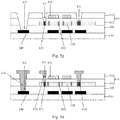
Fig. 3a and Fig. 3b are structural views of an array substrate in the present disclosure, respectively. -
Fig. 4 is a top view of the array substrate shown inFig. 3a . -
Figs. 5a, 5b, 5c, 5d ,5e, 5f ,5g, 5h ,5i, 5j , and5k are structural views of an array substrate after each step of a method in Example 1 of the present disclosure. -
Figs. 6a ,6b, and 6c are structural views of an array substrate after each step of a method in Example 2 of the present disclosure. - The following description is presented to enable any person skilled in the art to make and use the invention, and is provided in the context of a particular application and its requirements. Various modifications to the disclosed embodiments will be readily apparent to those skilled in the art, and the general principles defined herein may be applied to other embodiments and applications without departing from the spirit and scope of the present invention. Thus, the present invention is not limited to the embodiments shown, but is to be accorded the widest scope consistent with the claims.
- An array substrate of the present disclosure, as shown in
Fig. 3a, Fig. 3b , andFig. 4 (a top view of the array substrate shown inFig. 3a ), comprises asubstrate 100, and ametal shielding layer 200, abuffer layer 300, a top-gate thin film transistor, and acommon electrode 500 which are arranged on thesubstrate 100 successively. A source/drain electrode 410 of the top-gate thin film transistor is arranged over anactive layer 420, and is electrically connected with theactive layer 420 by means of a first via V1 penetrating a first insulatinglayer 610 between the source/drain electrode 410 and theactive layer 420. The array substrate further comprises afirst connection part 510, which is arranged in the same layer as the source/drain electrode 410, is used for electrically connecting themetal shielding layer 200 and thecommon electrode 500, and is electrically connected with themetal shielding layer 200 by means of a second via V2 penetrating the first insulatinglayer 610 and thebuffer layer 300. - In the above array substrate of the present disclosure, the metal shielding layer is electrically connected with the common electrode. Besides, the first connection part used for electrically connecting the metal shielding layer and the common electrode is arranged in the same layer as the source/drain electrode, and is electrically connected with the metal shielding electrode by means of a via penetrating the first insulating layer and the buffer layer. In this manner, the present array substrate can form a storage capacitor between the active layer and the metal shielding layer, thus increasing capacitance of the array substrate. In addition, the first connection part and the source/drain electrode which are arranged in the same layer can be formed by performing a patterning process for one time, thus reducing the fabricating flow, simplifying the fabricating process, saving the fabricating cost, and decreasing the fabricating time.
- It is noted that, in the present array substrate, as shown in
Fig. 3a and Fig. 3b , an orthographic projection of themetal shielding layer 200 onto thesubstrate 100 at least partially overlaps an orthographic projection of theactive layer 420 onto thesubstrate 100, so that a storage capacitor is formed between theactive layer 420 and themetal shielding layer 200. - In practice of the present array substrate, the active layer can be made from LTPS or oxide, and the present disclosure is not limited in this aspect.
- In the present array substrate, as shown in
Fig. 3a and Fig. 3b , there can be only one gate electrode. In practice, there can be twogate electrodes 430. The purpose of providing twogate electrodes 430 is to reduce leakage current of the thin film transistor. - In the present array substrate, as shown in
Fig. 3a, and Fig. 3b , theactive layer 420 may comprise heavily dopedregions 421 and lightly dopedregions 422. The heavily dopedregions 421 are arranged in theactive layer 420 at regions corresponding to the source/drain electrode 410, for reducing contact resistance between the source/drain electrode 410 and theactive layer 420. The lightly dopedregions 422 are provided between the heavily dopedregions 421, and arranged at both sides of the regions corresponding to twogate electrodes 430 in theactive layer 420. The lightly dopedregions 422 can reduce the leakage current in the thin film transistor. The arrangement of heavily dopedregions 421 and lightly dopedregions 422 as shown is only an example. In practice, in some thin film transistors, there is no heavily doped region or lightly doped region. Alternatively, there are more heavily doped regions or lightly doped regions which are arranged at different positions as required. - In particular, in the top-gate thin film transistor, the gate electrode can be arranged over the source/drain electrode, or below the source/drain electrode. Hereinafter, reference is made to a case in which the gate electrode lies below the source/drain electrode.
- In particular, when the gate electrode lies below the source/drain electrode, as shown in
Fig. 3a and Fig. 3b , the first insulatinglayer 610 between the source/drain electrode 410 and theactive layer 420 refers to agate insulating layer 611 between theactive layer 420 and agate electrode 430 and aninterlayer dielectric layer 612 between thegate electrode 430 and the source/drain electrode 410. However, the present disclosure is not limited in this aspect. - The present array substrate, as shown in
Fig. 3a , further comprises a second insulatinglayer 620 between the source/drain electrode 410 and thecommon electrode 500, wherein thecommon electrode 500 is electrically connected with thefirst connection part 510 by means of a third via V3 penetrating the second insulatinglayer 620. - For purpose of facilitating implementation, the present array substrate as shown in
Fig. 3a can further comprise: apixel electrode 700 which is arranged over thecommon electrode 500, a thirdinsulating layer 630 which is arranged between thepixel electrode 700 and thecommon electrode 500, and asecond connection part 710 which is arranged in the same layer as thecommon electrode 500 and is used for electrically connecting thepixel electrode 700 and a drain electrode in the source/drain electrode 410. Thesecond connection part 710 is electrically connected with a drain electrode in the source/drain electrode 410 by means of a fourth via V4 penetrating the second insulatinglayer 620, and thepixel electrode 700 is electrically connected with thesecond connection part 710 by means of a fifth via V5 penetrating the third insulatinglayer 630. - In practice of the present array substrate, in case the pixel electrode is arranged over the common electrode, the pixel electrode can have a slit shape, the pixel electrode can be made from a transparent conductive material like indium tin oxide, the common electrode can have a plate shape or slit shape, and the common electrode can be made from a transparent conductive material like indium tin oxide.
- For example, as shown in
Fig. 3b , the array substrate can further comprise: thepixel electrode 700 which is arranged between the source/drain electrode 410 and thecommon electrode 500 and is insulated from thecommon electrode 500, and the second insulatinglayer 620 which is arranged between thepixel electrode 700 and the source/drain electrode 410. Thepixel electrode 700 is electrically connected with the drain electrode in the source/drain electrode 410 by means of a sixth via V6 penetrating the second insulatinglayer 620. - As shown in
Fig. 3b , the array substrate can further comprise: the third insulatinglayer 630 which is arranged between thepixel electrode 700 and thecommon electrode 500, and athird connection part 520 which is arranged in the same layer as thepixel electrode 700 and is used for electrically connecting thecommon electrode 500 and thefirst connection part 510. Thethird connection part 520 is electrically connected with thefirst connection part 510 by means of a seventh via V7 penetrating the second insulatinglayer 620. Thecommon electrode 500 is electrically connected with thethird connection part 520 by means of an eighth via V8 penetrating the third insulatinglayer 630. - In practice of the present array substrate, in case the common electrode is arranged over the pixel electrode, the common electrode can have a slit shape, the common electrode can be made from a transparent conductive material like indium tin oxide, the pixel electrode can have a plate shape or slit shape, and the pixel electrode can be made from a transparent conductive material like indium tin oxide.
- It is noted that the present array substrate is described in case the top-gate TFT has an active layer of poly-crystalline silicon. However, the present disclosure is also applicable to a top-gate TFT has an active layer of amorphous silicon.
- Based on the same inventive concept, the present disclosure further provides a display device which comprises the array substrate as described above. The display device can be any product or component with a display function, such as a mobile phone, a tablet computer, a television, a monitor, a notebook computer, a digital photo frame, and a navigator. It will be appreciated by the skilled in the art that the display device may comprise other essential components. Thus, these components are not described in detail herein for simplicity, and do not limit the present disclosure in any way. The display device can be implemented in a manner similar with the array substrate as mentioned above.
- Based on the same inventive concept, the present disclosure further provides a method for fabricating an array substrate, comprising forming an a substrate successively patterns of a metal shielding layer, a buffer layer, a top-gate thin film transistor, and a common electrode; wherein in the top-gate thin film transistor, a source/drain electrode is arranged over an active layer and is electrically connected with the active layer by means of a first via penetrating a first insulating layer between the source/drain electrode and the active layer, wherein the method further comprises:
- at the same time as forming the first via penetrating the first insulating layer, forming a second via penetrating the first insulating layer and the buffer layer by means of a half tone mask plate or a gray tone mask plate; and
- at the same time as forming a pattern of the source/drain electrode, forming, by performing a patterning process for one time, a pattern of a first connection part which is used for electrically connecting the metal shielding layer and the common electrode and is electrically connected with the metal shielding layer by means of the second via.
- In the above mentioned method, at the same time as forming the first via penetrating the first insulating layer, the second via penetrating the first insulating layer and the buffer layer is formed by means of a half tone mask plate or a gray tone mask plate. At the same time as forming the pattern of the source/drain electrode, the pattern of the first connection part, which is used for electrically connecting the metal shielding layer and the common electrode and is electrically connected with the metal shielding layer by means of the second via, is formed by performing a patterning process for one time. Therefore, as compared with the prior art in which the metal shielding layer and the common electrode are electrically connected with each other by means of a first connection part and a second connection part on the first connection part, a mask process which separately forms a via for electrically connecting a first connection part and a metal shielding layer can be omitted in the present method. Therefore, the present method can reduce the fabricating flow, simplify the fabricating process, save the fabricating cost, and decrease the fabricating time.
- It is noted that in the present method, the patterning process can only comprise photolithographic process. Alternatively, the patterning process can comprise photolithographic process and etching steps. In addition, the patterning process can further comprise a process for forming a predefined pattern, like printing, ink-jetting. The photolithographic process refers to a process which comprises forming a film, exposing, developing and forms the pattern by means of photoresist, mask plate, exposure machine. In practice, a patterning process can be selected according to the structure to be formed in the present disclosure.
- The present method can further comprise: forming a thin film for a second insulating layer between the source/drain electrode and the common electrode to be formed; and forming a third via penetrating the thin film of the second insulating layer by performing a patterning process, wherein the common electrode is electrically connected with the first connection part by means of the third via.
- To simplify the fabricating process, save the fabricating cost, and decrease the production cycle, the present method can further comprise: at the same time as forming the third via, forming, by performing a patterning process for one time, a fourth via penetrating the second insulating layer; at the same time as forming the pattern of the common electrode, forming, by performing a patterning process for one time, a pattern of a second connection part which is used for electrically connecting a pixel electrode to be formed and a drain electrode in the source/drain electrode, wherein the second connection part is electrically connected with the drain electrode by means of the fourth via;
after forming the pattern of the common electrode, the method further comprises: forming a thin film of a third insulating layer on the common electrode; forming a fifth via penetrating the thin film of the third insulating layer by performing a patterning process; and forming a pattern of the pixel electrode on the third insulating layer, wherein the pixel electrode is electrically connected with the second connection part by means of the fifth via - Alternatively, after forming the pattern of the source/drain electrode, and before forming the pattern of the common electrode, the present method can further comprise: forming a thin film for a second insulating layer between the source/drain electrode and the common electrode to be formed; forming, by performing a patterning process, a sixth via penetrating the thin film of the second insulating layer; and forming a pattern of a pixel electrode on the thin film of the second insulating layer in which the sixth via has been formed, wherein the pixel electrode is electrically connected with a drain electrode in the source/drain electrode by means of the sixth via.
- To simplify the fabricating process, save the fabricating cost, and decrease the production cycle, the present method can further comprise: at the same time as forming the sixth via, forming, by performing a patterning process for one time, a seventh via penetrating the second insulating layer; and at the same time as forming the pattern of the pixel electrode, forming, by performing a patterning process for one time, a pattern of a third connection part which is used for electrically connecting the common electrode to be formed and the first connection part, wherein the third connection part is electrically connected with the first connection part by means of the seventh via;
after forming the pattern of the pixel electrode, the method further comprises: forming a thin film of a third insulating layer between the pixel electrode and the common electrode to be formed; and forming, by performing a patterning process, an eighth via penetrating the thin film of the third insulating layer, wherein the common electrode to be formed is electrically connected with the third connection part by means of the eighth via. - It is noted that reference has been made to a top-gate LTPS TFT with two gates. It will be appreciated that the present disclosure is also applicable to amorphous silicon TFT or oxide TFT which has a single gate and of the top-gate type. All solutions which can increase the storage capacitance of the array substrate by increasing a confronting area between the active layer and the metal shielding layer fall within the scope of the present disclosure.
- In particular, the method for fabricating an array substrate will be described by referring to an array substrate shown in
Fig. 3a and Fig. 3b . - As shown in
Fig. 3a , thepixel electrode 700 in the array substrate is arranged over thecommon electrode 500. The process for fabricating the array substrate may comprise the following steps. - (1) A pattern of the
metal shielding layer 200 is formed on thesubstrate 100, as shown inFig. 5a . - (2) A
buffer layer 300 is formed on themetal shielding layer 200, as shown inFig. 5b .
In practice, the buffer layer can be deposited by plasma enhanced chemical vapor deposition. The buffer layer can be made from silicon dioxide or silicon nitride. - (3) A pattern of an
active layer 420 is formed on thebuffer layer 300, as shown inFig. 5c .
In practice, a thin film of amorphous silicon is formed over the buffer layer by plasma enhanced chemical vapor deposition or similar methods. The amorphous silicon is crystallized by laser annealing process or solid phase crystallization process to form a poly-crystalline silicon thin film. The poly-crystalline silicon thin film is formed into a pattern comprising a LTPS active layer by a patterning process. - (4) A
gate insulating layer 611 is formed on theactive layer 420, as shown inFig. 5d .
In practice, the gate insulating layer can be made from silicon oxide or silicon nitride. - (5) A pattern of the
gate electrode 430 is formed on thegate insulating layer 611, as shown inFig. 5e .
In practice, the gate electrode can be made from a metal like molybdenum (Mo), aluminum (Al), or chromium (Cr). - (6) Heavily doped
regions 421 and lightly dopedregions 422 are formed in theactive layer 420, as shown inFig. 5f .
In practice, the active layer is heavily doped at both sides by ion implantation to form the heavily doped regions, and a portion of the active layer between the heavily doped regions is lightly doped to form the lightly doped regions. The lightly doped regions are arranged at both sides of a region corresponding to the gate electrode. During ion implantation, regions can be doped to different concentrations by ion implantation with a mask plate. Alternatively, the ion implantation can be performed by utilizing the pattern of the gate electrode for shielding, or by utilizing a photoresist in a patterning process for shielding, which is similar with the prior art and is omitted here for simplicity. - (7) An
interlayer dielectric layer 612 is formed on thegate electrode 430, and a first via V1 penetrating theinterlayer dielectric layer 612 and agate insulating layer 611 and a second via V2 penetrating theinterlayer dielectric layer 612, thegate insulating layer 611, and thebuffer layer 300 are formed by means of a half tone mask plate or a gray tone mask plate, as shown inFig. 5g .
In practice, a partially transparent region of the half tone mask plate or the gray tone mask plate corresponds to a region of the first via, and the completely transparent region corresponds to a region of the second via.
In practice, the interlayer dielectric layer can be made from silicon oxide or silicon nitride, and the present disclosure does not intend to be limited in this aspect. - (8) A pattern of a source/
drain electrode 410 and afirst connection part 510 is formed on theinterlayer dielectric layer 612, as shown inFig. 5h .
In practice, a thin film of the source/drain electrode can be formed on the interlayer dielectric layer. By performing a patterning process for one time, the pattern of the source/drain electrode and the first connection part can be formed in the thin film of the source/drain electrode. The source/drain electrode is electrically connected with the active layer by means of the first via, and the first connection part is electrically connected with the metal shielding layer by means of the second via. - (9) A thin film of a second insulating
layer 620 is formed on the source/drain electrode 410, and a third via V3 and a fourth via V4 penetrating the second insulatinglayer 620 are formed by performing a patterning process for one time, as shown inFig. 5i . - (10) A thin film of the
common electrode 500 is formed on the second insulatinglayer 620. A pattern of thecommon electrode 500 and asecond connection part 710 are formed in the thin film of thecommon electrode 500, by performing a patterning process for one time, as shown inFig. 5j .
In practice, the common electrode can have a plate shape or slit shape, the common electrode can be made from a transparent conductive material like indium tin oxide, the common electrode is electrically connected with the first connection part by means of the third via, and the second connection part is electrically connected with the drain electrode in the source/drain electrode by means of the fourth via. - (11) A third insulating
layer 630 is formed on thecommon electrode 500. A fifth via V5 penetrating the third insulatinglayer 630 is formed by performing a patterning process, as shown inFig. 5k . - (12) A pattern of the
pixel electrode 700 is formed on the third insulatinglayer 630, as shown inFig. 3a . - In practice, the pixel electrode can have a slit shape, the pixel electrode can be made from a transparent conductive material like indium tin oxide, and the pixel electrode is electrically connected with the second connection part by means of the fifth via.
- In particular, as a result of the above steps (1)-(12), the array substrate of the present disclosure is obtained. In particular, a structural view of the resultant array substrate is shown in
Fig. 3a . - As shown in
Fig. 3b , in the array substrate, thecommon electrode 500 is arranged over thepixel electrode 700. Apart from the above steps (1)-(8), the fabricating process of the array substrate further comprises the following steps. - (9') A thin film of the second insulating
layer 620 is formed on the source/drain electrode 410. The sixth via V6 and the seventh via V7 penetrating the second insulatinglayer 620 are formed by performing a patterning process for one time, as shown inFig. 6a . - (10') A thin film of the
pixel electrode 700 is formed on the second insulatinglayer 620. The pattern of thepixel electrode 700 and thethird connection part 520 is formed in the thin film of thepixel electrode 700 by performing a patterning process for one time, as shown inFig. 6b .
In practice, the pixel electrode can have a plate shape or slit shape, the pixel electrode can be made from a transparent conductive material like indium tin oxide, the pixel electrode is electrically connected with the drain electrode in the source/drain electrode by means of the sixth via, and the third connection part is electrically connected with the first connection part by means of the seventh via. - (11') A third insulating
layer 630 is formed on thepixel electrode 700. An eighth via V8 penetrating the third insulatinglayer 630 is formed by performing a patterning process, as shown inFig. 6c . - (12') A pattern of the
common electrode 500 is formed on the third insulatinglayer 630, as shown inFig. 3b . - In practice, the common electrode can have a slit shape, the common electrode can be made from a transparent conductive material like indium tin oxide, and the common electrode is electrically connected with the third connection part by means of the eighth via.
- In particular, as a result of the above steps (1)-(8) and (9')-(12'), the array substrate of the present disclosure is obtained. In particular, a structural view of the resultant array substrate is shown in
Fig. 3b . - The present disclosure provides an array substrate, a method for fabricating the same, and a display device. The metal shielding layer is electrically connected with the common electrode. Besides, the first connection part used for electrically connecting the metal shielding layer and the common electrode is arranged in the same layer as the source/drain electrode, and is electrically connected with the metal shielding electrode by means of a via penetrating the first insulating layer and the buffer layer. In this manner, the present array substrate can form a storage capacitor between the active layer and the metal shielding layer, thus increasing capacitance of the array substrate. In addition, the first connection part and the source/drain electrode which are arranged in the same layer can be formed by performing a patterning process for one time, thus reducing the fabricating flow, simplifying the fabricating process, saving the fabricating cost, and decreasing the fabricating time.
- The scope of the disclosure is defined by the appended claims rather than by the description, and all variations that fall within the range of the claims are intended to be embraced therein. Thus, other embodiments than the specific ones described above are equally possible within the scope of these appended claims.
Claims (11)
- An array substrate, comprising a substrate, and a metal shielding layer, a buffer layer, a top-gate thin film transistor, and a common electrode which are arranged on the substrate successively; wherein in the top-gate thin film transistor, a source/drain electrode is arranged over an active layer and is electrically connected with the active layer by means of a first via penetrating a first insulating layer between the source/drain electrode and the active layer, wherein the array substrate further comprises:a first connection part which is arranged in the same layer as the source/drain electrode, is used for electrically connecting the metal shielding layer and the common electrode, and is electrically connected with the metal shielding layer by means of a second via penetrating the first insulating layer and the buffer layer.
- The array substrate of claim 1, further comprising a second insulating layer which is arranged between the source/drain electrode and the common electrode, wherein the common electrode is electrically connected with the first connection part by means of a third via penetrating the second insulating layer.
- The array substrate of claim 2, further comprising: a pixel electrode which is arranged over the common electrode, a third insulating layer which is arranged between the pixel electrode and the common electrode, and a second connection part which is arranged in the same layer as the common electrode and is used for electrically connecting the pixel electrode and a drain electrode of the source/drain electrode,
wherein the second connection part is electrically connected with a drain electrode of the source/drain electrode by means of a fourth via penetrating the second insulating layer, and the pixel electrode is electrically connected with the second connection part by means of a fifth via penetrating the third insulating layer. - The array substrate of claim 1, further comprising: a pixel electrode which is arranged between the source/drain electrode and the common electrode and is insulated from the common electrode, and a second insulating layer which is arranged between the pixel electrode and the source/drain electrode,
wherein the pixel electrode is electrically connected with a drain electrode of the source/drain electrode by means of a sixth via penetrating the second insulating layer. - The array substrate of claim 4, further comprising: a third insulating layer which is arranged between the pixel electrode and the common electrode, and a third connection part which is arranged in the same layer as the pixel electrode and is used for electrically connecting the common electrode and the first connection part,
wherein the third connection part is electrically connected with the first connection part by means of a seventh via penetrating the second insulating layer, and the common electrode is electrically connected with the third connection part by means of an eighth via penetrating the third insulating layer. - A display device, comprising the array substrate of claim 1.
- A method for fabricating an array substrate, comprising forming an a substrate successively patterns of a metal shielding layer, a buffer layer, a top-gate thin film transistor, and a common electrode; wherein in the top-gate thin film transistor, a source/drain electrode is arranged over an active layer and is electrically connected with the active layer by means of a first via penetrating a first insulating layer between the source/drain electrode and the active layer, wherein the method further comprises:at the same time as forming the first via penetrating the first insulating layer, forming a second via penetrating the first insulating layer and the buffer layer by means of a half tone mask plate or a gray tone mask plate; andat the same time as forming a pattern of the source/drain electrode, forming, by performing a patterning process for one time, a pattern of a first connection part which is used for electrically connecting the metal shielding layer and the common electrode and is electrically connected with the metal shielding layer by means of the second via.
- The method of claim 7, wherein after forming the pattern of the source/drain electrode, and before forming the pattern of the common electrode, the method further comprises:forming a thin film for a second insulating layer between the source/drain electrode and the common electrode to be formed; andforming a third via penetrating the thin film of the second insulating layer by performing a patterning process, wherein the common electrode is electrically connected with the first connection part by means of the third via.
- The method of claim 8, further comprising:at the same time as forming the third via, forming, by performing a patterning process for one time, a fourth via penetrating the second insulating layer;at the same time as forming the pattern of the common electrode, forming, by performing a patterning process for one time, a pattern of a second connection part which is used for electrically connecting a pixel electrode to be formed and a drain electrode in the source/drain electrode, wherein the second connection part is electrically connected with the drain electrode by means of the fourth via;after forming the pattern of the common electrode, the method further comprises:forming a thin film of a third insulating layer on the common electrode;forming a fifth via penetrating the thin film of the third insulating layer by performing a patterning process; andforming a pattern of the pixel electrode on the third insulating layer, wherein the pixel electrode is electrically connected with the second connection part by means of the fifth via.
- The method of claim 7, wherein after forming the pattern of the source/drain electrode, and before forming the pattern of the common electrode, the method further comprises:forming a thin film for a second insulating layer between the source/drain electrode and the common electrode to be formed;forming, by performing a patterning process, a sixth via penetrating the thin film of the second insulating layer; andforming a pattern of a pixel electrode on the thin film of the second insulating layer in which the sixth via has been formed, wherein the pixel electrode is electrically connected with a drain electrode in the source/drain electrode by means of the sixth via.
- The method of claim 10, further comprising:at the same time as forming the sixth via, forming, by performing a patterning process for one time, a seventh via penetrating the second insulating layer; andat the same time as forming the pattern of the pixel electrode, forming, by performing a patterning process for one time, a pattern of a third connection part which is used for electrically connecting the common electrode to be formed and the first connection part, wherein the third connection part is electrically connected with the first connection part by means of the seventh via;after forming the pattern of the pixel electrode, the method further comprises:forming a thin film of a third insulating layer between the pixel electrode and the common electrode to be formed; andforming, by performing a patterning process, an eighth via penetrating the thin film of the third insulating layer, wherein the common electrode to be formed is electrically connected with the third connection part by means of the eighth via.
Applications Claiming Priority (2)
| Application Number | Priority Date | Filing Date | Title |
|---|---|---|---|
| CN201410232647.7A CN104022126B (en) | 2014-05-28 | 2014-05-28 | Array substrate and manufacturing method thereof, and display apparatus |
| PCT/CN2014/085088 WO2015180269A1 (en) | 2014-05-28 | 2014-08-25 | Array substrate and manufacturing method therefor, and display apparatus |
Publications (2)
| Publication Number | Publication Date |
|---|---|
| EP3171398A1 true EP3171398A1 (en) | 2017-05-24 |
| EP3171398A4 EP3171398A4 (en) | 2018-04-11 |
Family
ID=51438796
Family Applications (1)
| Application Number | Title | Priority Date | Filing Date |
|---|---|---|---|
| EP14861186.6A Withdrawn EP3171398A4 (en) | 2014-05-28 | 2014-08-25 | Array substrate and manufacturing method therefor, and display apparatus |
Country Status (4)
| Country | Link |
|---|---|
| US (1) | US20160276376A1 (en) |
| EP (1) | EP3171398A4 (en) |
| CN (1) | CN104022126B (en) |
| WO (1) | WO2015180269A1 (en) |
Families Citing this family (20)
| Publication number | Priority date | Publication date | Assignee | Title |
|---|---|---|---|---|
| CN104393020B (en) | 2014-11-21 | 2017-07-04 | 京东方科技集团股份有限公司 | A kind of array base palte and preparation method thereof, display device |
| CN104503172A (en) * | 2014-12-19 | 2015-04-08 | 深圳市华星光电技术有限公司 | Array substrate and display device |
| CN104460157B (en) * | 2014-12-19 | 2019-09-10 | 深圳市华星光电技术有限公司 | Array substrate and display device |
| CN204391121U (en) * | 2014-12-22 | 2015-06-10 | 京东方科技集团股份有限公司 | A kind of display unit, array base palte and thin-film transistor |
| CN104576542B (en) * | 2015-01-26 | 2018-12-18 | 合肥鑫晟光电科技有限公司 | Array substrate and preparation method thereof, display device |
| CN104716196B (en) * | 2015-03-18 | 2017-08-08 | 京东方科技集团股份有限公司 | Thin film transistor (TFT) and preparation method thereof, array base palte and display device |
| KR102391347B1 (en) * | 2015-04-09 | 2022-04-28 | 삼성디스플레이 주식회사 | Thin film transistor array substrate and display apparatus using the same |
| CN104867944B (en) * | 2015-05-08 | 2018-07-10 | 深圳市华星光电技术有限公司 | Array base-plate structure and preparation method thereof |
| CN105161505B (en) | 2015-09-28 | 2018-11-23 | 京东方科技集团股份有限公司 | A kind of array substrate and preparation method thereof, display panel |
| CN106154669A (en) * | 2016-09-14 | 2016-11-23 | 厦门天马微电子有限公司 | Array base palte and preparation method thereof, liquid crystal indicator |
| HK1251814A1 (en) * | 2016-11-17 | 2019-03-29 | 華為技術有限公司 | Array substrate and preparation method therefor, and liquid crystal display panel |
| CN108133932B (en) * | 2016-12-01 | 2020-04-10 | 京东方科技集团股份有限公司 | Array substrate, manufacturing method thereof and display panel |
| CN106920804B (en) * | 2017-04-28 | 2020-03-24 | 厦门天马微电子有限公司 | Array substrate, driving method thereof, display panel and display device |
| KR102635447B1 (en) * | 2018-06-25 | 2024-02-08 | 삼성디스플레이 주식회사 | Method for manufacturing organic light emitting display |
| CN109037297B (en) | 2018-08-09 | 2021-01-29 | 京东方科技集团股份有限公司 | An organic light-emitting display substrate and a manufacturing method thereof |
| CN109065590B (en) * | 2018-08-09 | 2020-12-04 | 京东方科技集团股份有限公司 | Organic light-emitting display substrate and method of making the same, and organic light-emitting display device |
| CN109545803B (en) * | 2018-12-29 | 2020-10-13 | 武汉华星光电技术有限公司 | Array substrate and manufacturing method thereof |
| KR102819878B1 (en) | 2019-03-15 | 2025-06-12 | 삼성디스플레이 주식회사 | Display device |
| CN114709223A (en) * | 2022-03-29 | 2022-07-05 | Tcl华星光电技术有限公司 | Display panel, preparation method thereof and display device |
| CN121127794A (en) * | 2024-04-11 | 2025-12-12 | 京东方科技集团股份有限公司 | Display substrate and display device |
Family Cites Families (32)
| Publication number | Priority date | Publication date | Assignee | Title |
|---|---|---|---|---|
| KR100202236B1 (en) * | 1996-04-09 | 1999-07-01 | 구자홍 | Active matrix panel and its making method |
| JP3708637B2 (en) * | 1996-07-15 | 2005-10-19 | 株式会社半導体エネルギー研究所 | Liquid crystal display device |
| JP3883244B2 (en) * | 1997-01-23 | 2007-02-21 | エルジー フィリップス エルシーディー カンパニー リミテッド | Liquid crystal display |
| US6433841B1 (en) * | 1997-12-19 | 2002-08-13 | Seiko Epson Corporation | Electro-optical apparatus having faces holding electro-optical material in between flattened by using concave recess, manufacturing method thereof, and electronic device using same |
| JPH11326954A (en) * | 1998-05-15 | 1999-11-26 | Semiconductor Energy Lab Co Ltd | Semiconductor device |
| JP3141860B2 (en) * | 1998-10-28 | 2001-03-07 | ソニー株式会社 | Manufacturing method of liquid crystal display device |
| US6590229B1 (en) * | 1999-01-21 | 2003-07-08 | Semiconductor Energy Laboratory Co., Ltd. | Semiconductor device and process for production thereof |
| JP3591513B2 (en) * | 2000-04-21 | 2004-11-24 | セイコーエプソン株式会社 | Electro-optical device and projector |
| US6636284B2 (en) * | 2000-08-11 | 2003-10-21 | Seiko Epson Corporation | System and method for providing an electro-optical device having light shield layers |
| US6583440B2 (en) * | 2000-11-30 | 2003-06-24 | Seiko Epson Corporation | Soi substrate, element substrate, semiconductor device, electro-optical apparatus, electronic equipment, method of manufacturing the soi substrate, method of manufacturing the element substrate, and method of manufacturing the electro-optical apparatus |
| JP2002299632A (en) * | 2001-03-30 | 2002-10-11 | Sanyo Electric Co Ltd | Semiconductor device and active matrix display device |
| TW594336B (en) * | 2002-01-30 | 2004-06-21 | Sanyo Electric Co | Semiconductor display device, method for making the same, and active matrix type display device |
| JP3788387B2 (en) * | 2002-05-10 | 2006-06-21 | セイコーエプソン株式会社 | Electro-optical device and method of manufacturing electro-optical device |
| JP3858880B2 (en) * | 2002-10-31 | 2006-12-20 | セイコーエプソン株式会社 | Electro-optical device and electronic apparatus |
| JP4423659B2 (en) * | 2003-01-31 | 2010-03-03 | 日本電気株式会社 | Thin film transistor, TFT substrate, and liquid crystal display device |
| KR101242030B1 (en) * | 2006-06-22 | 2013-03-11 | 엘지디스플레이 주식회사 | Organic Electroluminescent Device |
| TWI374544B (en) * | 2006-11-13 | 2012-10-11 | Au Optronics Corp | Thin film transistor array substrates and fbricating method thereof |
| US8110832B2 (en) * | 2007-02-22 | 2012-02-07 | Seiko Epson Corporation | Electro-optical substrate, method for designing the same, electro-optical device, and electronic apparatus |
| KR101460138B1 (en) * | 2007-04-10 | 2014-11-10 | 삼성디스플레이 주식회사 | Display substrate, liquid crystal display including the same, and manufacturing method thereof |
| KR101458898B1 (en) * | 2008-02-12 | 2014-11-07 | 삼성디스플레이 주식회사 | Display device and manufacturing method thereof |
| KR101529957B1 (en) * | 2008-02-18 | 2015-06-18 | 삼성디스플레이 주식회사 | Liquid crystal display |
| JP2010015019A (en) * | 2008-07-04 | 2010-01-21 | Hitachi Displays Ltd | Liquid crystal display device and manufacturing method for the same |
| US9136286B2 (en) * | 2009-08-07 | 2015-09-15 | Semiconductor Energy Laboratory Co., Ltd. | Display panel and electronic book |
| JP5855888B2 (en) * | 2011-09-30 | 2016-02-09 | 株式会社ジャパンディスプレイ | Liquid crystal display |
| JP2013080040A (en) * | 2011-10-03 | 2013-05-02 | Seiko Epson Corp | Electrooptical device, method for manufacturing electrooptical device, and electronic equipment |
| CN102569187B (en) * | 2011-12-21 | 2014-08-06 | 深圳市华星光电技术有限公司 | Low-temperature polysilicon display device and manufacturing method thereof |
| CN103309108B (en) * | 2013-05-30 | 2016-02-10 | 京东方科技集团股份有限公司 | Array base palte and manufacture method, display device |
| CN103383946B (en) * | 2013-07-12 | 2016-05-25 | 京东方科技集团股份有限公司 | The preparation method of a kind of array base palte, display unit and array base palte |
| CN203480182U (en) * | 2013-08-30 | 2014-03-12 | 京东方科技集团股份有限公司 | Array substrate and display device |
| CN103489824B (en) * | 2013-09-05 | 2016-08-17 | 京东方科技集团股份有限公司 | A kind of array base palte and preparation method thereof and display device |
| CN103499906B (en) * | 2013-10-15 | 2017-02-15 | 京东方科技集团股份有限公司 | Array substrate, manufacturing method of array substrate and display device |
| CN203871327U (en) * | 2014-05-28 | 2014-10-08 | 京东方科技集团股份有限公司 | Array substrate and display device |
-
2014
- 2014-05-28 CN CN201410232647.7A patent/CN104022126B/en active Active
- 2014-08-25 US US14/646,046 patent/US20160276376A1/en not_active Abandoned
- 2014-08-25 EP EP14861186.6A patent/EP3171398A4/en not_active Withdrawn
- 2014-08-25 WO PCT/CN2014/085088 patent/WO2015180269A1/en not_active Ceased
Also Published As
| Publication number | Publication date |
|---|---|
| CN104022126A (en) | 2014-09-03 |
| US20160276376A1 (en) | 2016-09-22 |
| EP3171398A4 (en) | 2018-04-11 |
| WO2015180269A1 (en) | 2015-12-03 |
| CN104022126B (en) | 2017-04-12 |
Similar Documents
| Publication | Publication Date | Title |
|---|---|---|
| US20160276376A1 (en) | Array substrate, method for fabricating the same, and display device | |
| EP2881785B1 (en) | Array substrate, manufacturing method therefor, and display apparatus | |
| US10818797B2 (en) | Thin film transistor and method of fabricating the same, array substrate and display device | |
| US9559125B2 (en) | Array substrate, display device, and method for manufacturing the array substrate | |
| US9620646B2 (en) | Array substrate, manufacturing method thereof and display device | |
| CN203871327U (en) | Array substrate and display device | |
| US7985636B2 (en) | Method for fabricating low temperature poly-silicon thin film transistor substrate | |
| US9911766B2 (en) | Array substrate and manufacturing method thereof, and display apparatus | |
| KR20180098621A (en) | Method for manufacturing low-temperature polysilicon array substrate | |
| US20160365458A1 (en) | Array substrate, method for producing the same and display device | |
| WO2016023305A1 (en) | Thin film transistor and manufacturing method thereof, array substrate and display device | |
| US20180292696A1 (en) | Array substrate, manufacturing method thereof, display panel and display device | |
| EP3457441B1 (en) | Thin film transistor and manufacturing method therefor, array substrate and manufacturing method therefor, and display apparatus | |
| WO2017128575A1 (en) | Manufacturing method for ltps array substrate | |
| US10629747B2 (en) | Thin film transistor, manufacturing method thereof, array substrate and manufacturing method thereof | |
| CN106024633A (en) | Preparation methods of thin film transistor and array substrate, array substrate and display device | |
| US6888161B2 (en) | Structure of TFT planar display panel | |
| WO2018133352A1 (en) | Array substrate and its fabricating method, display device | |
| US9653578B2 (en) | Thin film transistor, its manufacturing method and display device | |
| US9972643B2 (en) | Array substrate and fabrication method thereof, and display device | |
| US20210066504A1 (en) | Thin film transistor and manufacturing method thereof and display device | |
| US10205029B2 (en) | Thin film transistor, manufacturing method thereof, and display device | |
| US11043515B2 (en) | Display substrate, manufacturing method thereof, and display device | |
| US20120280332A1 (en) | Pixel structure and method for fabricating the same | |
| US20200091204A1 (en) | Array substrate, manufacturing method thereof, display panel and manufacturing method thereof |
Legal Events
| Date | Code | Title | Description |
|---|---|---|---|
| STAA | Information on the status of an ep patent application or granted ep patent |
Free format text: STATUS: THE INTERNATIONAL PUBLICATION HAS BEEN MADE |
|
| PUAI | Public reference made under article 153(3) epc to a published international application that has entered the european phase |
Free format text: ORIGINAL CODE: 0009012 |
|
| STAA | Information on the status of an ep patent application or granted ep patent |
Free format text: STATUS: REQUEST FOR EXAMINATION WAS MADE |
|
| 17P | Request for examination filed |
Effective date: 20150520 |
|
| AK | Designated contracting states |
Kind code of ref document: A1 Designated state(s): AL AT BE BG CH CY CZ DE DK EE ES FI FR GB GR HR HU IE IS IT LI LT LU LV MC MK MT NL NO PL PT RO RS SE SI SK SM TR |
|
| AX | Request for extension of the european patent |
Extension state: BA ME |
|
| RIN1 | Information on inventor provided before grant (corrected) |
Inventor name: CHEN, PENGJUN Inventor name: SUN, JIAN Inventor name: AN, SEONGJUN Inventor name: LI, CHENG |
|
| DAX | Request for extension of the european patent (deleted) | ||
| A4 | Supplementary search report drawn up and despatched |
Effective date: 20180314 |
|
| RIC1 | Information provided on ipc code assigned before grant |
Ipc: G02F 1/1362 20060101ALI20180308BHEP Ipc: G02F 1/1343 20060101ALN20180308BHEP Ipc: G02F 1/1368 20060101ALI20180308BHEP Ipc: H01L 27/12 20060101ALI20180308BHEP Ipc: H01L 21/77 20170101AFI20180308BHEP |
|
| STAA | Information on the status of an ep patent application or granted ep patent |
Free format text: STATUS: EXAMINATION IS IN PROGRESS |
|
| 17Q | First examination report despatched |
Effective date: 20200317 |
|
| STAA | Information on the status of an ep patent application or granted ep patent |
Free format text: STATUS: THE APPLICATION IS DEEMED TO BE WITHDRAWN |
|
| 18D | Application deemed to be withdrawn |
Effective date: 20210310 |