EP3168902A1 - Herstellungsverfahren einer elektrochemischen vorrichtung, wie etwa eines elektrochromsystems oder eines systems zur energiespeicherung, wie etwa eine mikrobatterie, eine batterie oder ein superkondensator - Google Patents
Herstellungsverfahren einer elektrochemischen vorrichtung, wie etwa eines elektrochromsystems oder eines systems zur energiespeicherung, wie etwa eine mikrobatterie, eine batterie oder ein superkondensator Download PDFInfo
- Publication number
- EP3168902A1 EP3168902A1 EP16198046.1A EP16198046A EP3168902A1 EP 3168902 A1 EP3168902 A1 EP 3168902A1 EP 16198046 A EP16198046 A EP 16198046A EP 3168902 A1 EP3168902 A1 EP 3168902A1
- Authority
- EP
- European Patent Office
- Prior art keywords
- elementary entities
- elementary
- entities
- substrate
- current collector
- Prior art date
- Legal status (The legal status is an assumption and is not a legal conclusion. Google has not performed a legal analysis and makes no representation as to the accuracy of the status listed.)
- Granted
Links
Images


Classifications
-
- H—ELECTRICITY
- H01—ELECTRIC ELEMENTS
- H01G—CAPACITORS; CAPACITORS, RECTIFIERS, DETECTORS, SWITCHING DEVICES, LIGHT-SENSITIVE OR TEMPERATURE-SENSITIVE DEVICES OF THE ELECTROLYTIC TYPE
- H01G11/00—Hybrid capacitors, i.e. capacitors having different positive and negative electrodes; Electric double-layer [EDL] capacitors; Processes for the manufacture thereof or of parts thereof
- H01G11/84—Processes for the manufacture of hybrid or EDL capacitors, or components thereof
-
- G—PHYSICS
- G02—OPTICS
- G02F—OPTICAL DEVICES OR ARRANGEMENTS FOR THE CONTROL OF LIGHT BY MODIFICATION OF THE OPTICAL PROPERTIES OF THE MEDIA OF THE ELEMENTS INVOLVED THEREIN; NON-LINEAR OPTICS; FREQUENCY-CHANGING OF LIGHT; OPTICAL LOGIC ELEMENTS; OPTICAL ANALOGUE/DIGITAL CONVERTERS
- G02F1/00—Devices or arrangements for the control of the intensity, colour, phase, polarisation or direction of light arriving from an independent light source, e.g. switching, gating or modulating; Non-linear optics
- G02F1/01—Devices or arrangements for the control of the intensity, colour, phase, polarisation or direction of light arriving from an independent light source, e.g. switching, gating or modulating; Non-linear optics for the control of the intensity, phase, polarisation or colour
- G02F1/15—Devices or arrangements for the control of the intensity, colour, phase, polarisation or direction of light arriving from an independent light source, e.g. switching, gating or modulating; Non-linear optics for the control of the intensity, phase, polarisation or colour based on an electrochromic effect
- G02F1/153—Constructional details
-
- H—ELECTRICITY
- H01—ELECTRIC ELEMENTS
- H01G—CAPACITORS; CAPACITORS, RECTIFIERS, DETECTORS, SWITCHING DEVICES, LIGHT-SENSITIVE OR TEMPERATURE-SENSITIVE DEVICES OF THE ELECTROLYTIC TYPE
- H01G11/00—Hybrid capacitors, i.e. capacitors having different positive and negative electrodes; Electric double-layer [EDL] capacitors; Processes for the manufacture thereof or of parts thereof
- H01G11/10—Multiple hybrid or EDL capacitors, e.g. arrays or modules
-
- H—ELECTRICITY
- H01—ELECTRIC ELEMENTS
- H01G—CAPACITORS; CAPACITORS, RECTIFIERS, DETECTORS, SWITCHING DEVICES, LIGHT-SENSITIVE OR TEMPERATURE-SENSITIVE DEVICES OF THE ELECTROLYTIC TYPE
- H01G11/00—Hybrid capacitors, i.e. capacitors having different positive and negative electrodes; Electric double-layer [EDL] capacitors; Processes for the manufacture thereof or of parts thereof
- H01G11/22—Electrodes
- H01G11/26—Electrodes characterised by their structure, e.g. multi-layered, porosity or surface features
- H01G11/28—Electrodes characterised by their structure, e.g. multi-layered, porosity or surface features arranged or disposed on a current collector; Layers or phases between electrodes and current collectors, e.g. adhesives
-
- H—ELECTRICITY
- H01—ELECTRIC ELEMENTS
- H01G—CAPACITORS; CAPACITORS, RECTIFIERS, DETECTORS, SWITCHING DEVICES, LIGHT-SENSITIVE OR TEMPERATURE-SENSITIVE DEVICES OF THE ELECTROLYTIC TYPE
- H01G11/00—Hybrid capacitors, i.e. capacitors having different positive and negative electrodes; Electric double-layer [EDL] capacitors; Processes for the manufacture thereof or of parts thereof
- H01G11/54—Electrolytes
- H01G11/56—Solid electrolytes, e.g. gels; Additives therein
-
- H—ELECTRICITY
- H01—ELECTRIC ELEMENTS
- H01G—CAPACITORS; CAPACITORS, RECTIFIERS, DETECTORS, SWITCHING DEVICES, LIGHT-SENSITIVE OR TEMPERATURE-SENSITIVE DEVICES OF THE ELECTROLYTIC TYPE
- H01G11/00—Hybrid capacitors, i.e. capacitors having different positive and negative electrodes; Electric double-layer [EDL] capacitors; Processes for the manufacture thereof or of parts thereof
- H01G11/54—Electrolytes
- H01G11/58—Liquid electrolytes
-
- H—ELECTRICITY
- H01—ELECTRIC ELEMENTS
- H01G—CAPACITORS; CAPACITORS, RECTIFIERS, DETECTORS, SWITCHING DEVICES, LIGHT-SENSITIVE OR TEMPERATURE-SENSITIVE DEVICES OF THE ELECTROLYTIC TYPE
- H01G11/00—Hybrid capacitors, i.e. capacitors having different positive and negative electrodes; Electric double-layer [EDL] capacitors; Processes for the manufacture thereof or of parts thereof
- H01G11/66—Current collectors
-
- H—ELECTRICITY
- H01—ELECTRIC ELEMENTS
- H01G—CAPACITORS; CAPACITORS, RECTIFIERS, DETECTORS, SWITCHING DEVICES, LIGHT-SENSITIVE OR TEMPERATURE-SENSITIVE DEVICES OF THE ELECTROLYTIC TYPE
- H01G11/00—Hybrid capacitors, i.e. capacitors having different positive and negative electrodes; Electric double-layer [EDL] capacitors; Processes for the manufacture thereof or of parts thereof
- H01G11/66—Current collectors
- H01G11/72—Current collectors specially adapted for integration in multiple or stacked hybrid or EDL capacitors
-
- H—ELECTRICITY
- H01—ELECTRIC ELEMENTS
- H01M—PROCESSES OR MEANS, e.g. BATTERIES, FOR THE DIRECT CONVERSION OF CHEMICAL ENERGY INTO ELECTRICAL ENERGY
- H01M10/00—Secondary cells; Manufacture thereof
- H01M10/04—Construction or manufacture in general
- H01M10/0436—Small-sized flat cells or batteries for portable equipment
-
- H—ELECTRICITY
- H01—ELECTRIC ELEMENTS
- H01M—PROCESSES OR MEANS, e.g. BATTERIES, FOR THE DIRECT CONVERSION OF CHEMICAL ENERGY INTO ELECTRICAL ENERGY
- H01M10/00—Secondary cells; Manufacture thereof
- H01M10/05—Accumulators with non-aqueous electrolyte
- H01M10/052—Li-accumulators
-
- H—ELECTRICITY
- H01—ELECTRIC ELEMENTS
- H01M—PROCESSES OR MEANS, e.g. BATTERIES, FOR THE DIRECT CONVERSION OF CHEMICAL ENERGY INTO ELECTRICAL ENERGY
- H01M10/00—Secondary cells; Manufacture thereof
- H01M10/05—Accumulators with non-aqueous electrolyte
- H01M10/052—Li-accumulators
- H01M10/0525—Rocking-chair batteries, i.e. batteries with lithium insertion or intercalation in both electrodes; Lithium-ion batteries
-
- H—ELECTRICITY
- H01—ELECTRIC ELEMENTS
- H01M—PROCESSES OR MEANS, e.g. BATTERIES, FOR THE DIRECT CONVERSION OF CHEMICAL ENERGY INTO ELECTRICAL ENERGY
- H01M10/00—Secondary cells; Manufacture thereof
- H01M10/05—Accumulators with non-aqueous electrolyte
- H01M10/058—Construction or manufacture
- H01M10/0585—Construction or manufacture of accumulators having only flat construction elements, i.e. flat positive electrodes, flat negative electrodes and flat separators
-
- H—ELECTRICITY
- H01—ELECTRIC ELEMENTS
- H01M—PROCESSES OR MEANS, e.g. BATTERIES, FOR THE DIRECT CONVERSION OF CHEMICAL ENERGY INTO ELECTRICAL ENERGY
- H01M50/00—Constructional details or processes of manufacture of the non-active parts of electrochemical cells other than fuel cells, e.g. hybrid cells
- H01M50/50—Current conducting connections for cells or batteries
- H01M50/502—Interconnectors for connecting terminals of adjacent batteries; Interconnectors for connecting cells outside a battery casing
- H01M50/509—Interconnectors for connecting terminals of adjacent batteries; Interconnectors for connecting cells outside a battery casing characterised by the type of connection, e.g. mixed connections
- H01M50/512—Connection only in parallel
-
- H—ELECTRICITY
- H01—ELECTRIC ELEMENTS
- H01M—PROCESSES OR MEANS, e.g. BATTERIES, FOR THE DIRECT CONVERSION OF CHEMICAL ENERGY INTO ELECTRICAL ENERGY
- H01M50/00—Constructional details or processes of manufacture of the non-active parts of electrochemical cells other than fuel cells, e.g. hybrid cells
- H01M50/50—Current conducting connections for cells or batteries
- H01M50/502—Interconnectors for connecting terminals of adjacent batteries; Interconnectors for connecting cells outside a battery casing
- H01M50/514—Methods for interconnecting adjacent batteries or cells
-
- H—ELECTRICITY
- H01—ELECTRIC ELEMENTS
- H01M—PROCESSES OR MEANS, e.g. BATTERIES, FOR THE DIRECT CONVERSION OF CHEMICAL ENERGY INTO ELECTRICAL ENERGY
- H01M50/00—Constructional details or processes of manufacture of the non-active parts of electrochemical cells other than fuel cells, e.g. hybrid cells
- H01M50/50—Current conducting connections for cells or batteries
- H01M50/502—Interconnectors for connecting terminals of adjacent batteries; Interconnectors for connecting cells outside a battery casing
- H01M50/521—Interconnectors for connecting terminals of adjacent batteries; Interconnectors for connecting cells outside a battery casing characterised by the material
- H01M50/522—Inorganic material
-
- H—ELECTRICITY
- H01—ELECTRIC ELEMENTS
- H01M—PROCESSES OR MEANS, e.g. BATTERIES, FOR THE DIRECT CONVERSION OF CHEMICAL ENERGY INTO ELECTRICAL ENERGY
- H01M6/00—Primary cells; Manufacture thereof
- H01M6/40—Printed batteries, e.g. thin film batteries
-
- H—ELECTRICITY
- H01—ELECTRIC ELEMENTS
- H01M—PROCESSES OR MEANS, e.g. BATTERIES, FOR THE DIRECT CONVERSION OF CHEMICAL ENERGY INTO ELECTRICAL ENERGY
- H01M2220/00—Batteries for particular applications
- H01M2220/30—Batteries in portable systems, e.g. mobile phone, laptop
-
- Y—GENERAL TAGGING OF NEW TECHNOLOGICAL DEVELOPMENTS; GENERAL TAGGING OF CROSS-SECTIONAL TECHNOLOGIES SPANNING OVER SEVERAL SECTIONS OF THE IPC; TECHNICAL SUBJECTS COVERED BY FORMER USPC CROSS-REFERENCE ART COLLECTIONS [XRACs] AND DIGESTS
- Y02—TECHNOLOGIES OR APPLICATIONS FOR MITIGATION OR ADAPTATION AGAINST CLIMATE CHANGE
- Y02E—REDUCTION OF GREENHOUSE GAS [GHG] EMISSIONS, RELATED TO ENERGY GENERATION, TRANSMISSION OR DISTRIBUTION
- Y02E60/00—Enabling technologies; Technologies with a potential or indirect contribution to GHG emissions mitigation
- Y02E60/10—Energy storage using batteries
-
- Y—GENERAL TAGGING OF NEW TECHNOLOGICAL DEVELOPMENTS; GENERAL TAGGING OF CROSS-SECTIONAL TECHNOLOGIES SPANNING OVER SEVERAL SECTIONS OF THE IPC; TECHNICAL SUBJECTS COVERED BY FORMER USPC CROSS-REFERENCE ART COLLECTIONS [XRACs] AND DIGESTS
- Y02—TECHNOLOGIES OR APPLICATIONS FOR MITIGATION OR ADAPTATION AGAINST CLIMATE CHANGE
- Y02E—REDUCTION OF GREENHOUSE GAS [GHG] EMISSIONS, RELATED TO ENERGY GENERATION, TRANSMISSION OR DISTRIBUTION
- Y02E60/00—Enabling technologies; Technologies with a potential or indirect contribution to GHG emissions mitigation
- Y02E60/13—Energy storage using capacitors
-
- Y—GENERAL TAGGING OF NEW TECHNOLOGICAL DEVELOPMENTS; GENERAL TAGGING OF CROSS-SECTIONAL TECHNOLOGIES SPANNING OVER SEVERAL SECTIONS OF THE IPC; TECHNICAL SUBJECTS COVERED BY FORMER USPC CROSS-REFERENCE ART COLLECTIONS [XRACs] AND DIGESTS
- Y02—TECHNOLOGIES OR APPLICATIONS FOR MITIGATION OR ADAPTATION AGAINST CLIMATE CHANGE
- Y02P—CLIMATE CHANGE MITIGATION TECHNOLOGIES IN THE PRODUCTION OR PROCESSING OF GOODS
- Y02P70/00—Climate change mitigation technologies in the production process for final industrial or consumer products
- Y02P70/50—Manufacturing or production processes characterised by the final manufactured product
Definitions
- the invention relates to a method for manufacturing electrochemical devices, such as electrochromic systems or systems for storing energy, for example microbatteries, batteries or supercapacitors, and to an electrochemical device thus obtained.
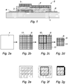
- Electrochromic systems and devices for storing energy are conventionally formed of a substrate 1 on which is disposed at least one stack of active layers 2, said stack comprising at least a first electrode 3 connected to a first current collector 4 and at least a second electrode 5 connected to a second current collector 6 ( figure 1 ).
- the electrodes are separated by an electrolytic membrane 7.
- the migration of one or more ions between the two electrodes 3, 5 through the electrolyte makes it possible to store energy or to deliver it (in the case of batteries, microbatteries / supercapacities) or to change the properties of the component, in particular the occurrence of optical properties in the case of electrochromic components.
- the documents WO2014099974 and EP2044642 describe manufacturing methods which consist in (i) depositing, in a first step, all the active layers (a first current collector, a first electrode, an electrolyte, a second electrode and a second current collector) so as to form a single stack of active layers on the entire surface of the substrate ("blanket deposition" mode), and (ii) proceed to the structuring of the layers without using masks, for example by laser ablation, so as to form several separate stacks active layers.
- the layers are simultaneously structured and connected by means of a head coupling a laser and an inkjet type deposition nozzle.
- the absence of masks or the use of masks other than mechanical ones makes it possible to reduce the costs, to improve the density of integration, and to have a yield independent of the particulate contamination of masks.
- the production rate is no longer limited by deposition parameters of the "mechanical mask” mode. Higher deposition rates can be obtained, but some deposition steps can nevertheless limit the speed of the process.
- each active layer is deposited on the entire surface of the substrate, if there is a lack of continuity in one of the layers, it can be generalized to all microbatteries formed after structuring from the same unique layers. If the defect is present in the electrolyte layer, the first and second electrodes may be in contact, causing a short circuit between the first and second electrodes, an uncontrolled migration of lithium ions between the two electrodes, and even a non-reversible saturation of one of the two ion electrodes that would make future structured batteries fail to share the same area of defects.
- the defect can extend laterally (isotropic and rapid diffusion of ions) to cover a wider area of the substrate and impact advantages of future batteries at the time of structuring
- each of the structuring steps is specific to a product type of a particular shape and size.
- the parameterization of the different stages induces a slowing down of the production rate.
- the document FR 2977380 describes a method of manufacturing a battery device with test of the operation of the batteries before their electrical connection so as not to connect the non-functional batteries.
- the document US5,350,645 proposes to make a multitude of identical lithium batteries on a substrate. After completion, the substrate is cut to separate the different individual batteries.
- the document US 2008/0263855 proposes forming batteries on two opposite sides of a substrate or adjacent to one and the same face of a substrate. After completion, the substrate is cut to separate the different individual batteries. Alternatively, groups of batteries are formed.
- the aim of the invention is to overcome the disadvantages of the prior art and, in particular, to propose a method for manufacturing electrochemical devices, such as electrochromic systems or systems for storing energy, for example microbatteries. , batteries or supercapacitors for mass producing high efficiency and low cost electrochemical devices of different sizes and shapes.
- electrochemical devices such as electrochromic systems or systems for storing energy, for example microbatteries.
- batteries or supercapacitors for mass producing high efficiency and low cost electrochemical devices of different sizes and shapes.
- the final device is not formed of a single structured entity to the desired size but of several elementary entities 8 connected in parallel.
- Each entire elementary entity 8 has a functional property Xi.
- the elementary entities 8 are connected in parallel, so as to give the electrochemical device a functional property Xf.
- the functional properties Xi, Xf are electrical, optical or electrochemical properties.
- the properties of the final device correspond to the association of the properties of the connected elementary entities 8.
- the substrate provided in step a) is silicon, glass, ceramic or metal ( figure 2a ).
- the substrate also called support substrate, is a monoblock, it forms a continuous element.
- the substrate is advantageously cleaned, for example chemically, in order to remove residues and / or particles, possibly present on its surface.
- a heat treatment step may also be applied to reduce the residual stresses and / or in addition to the cleaning step.
- a first group of elementary entities 8 is formed on the substrate 1 ( Figures 2b and 2e ).
- Elementary entities 8 can also be called elementary cells.
- the elementary entities 8 can have several possible forms. They advantageously have the shape of a polygon such as a rectangle or a rhombus. Even more advantageously, they have the shape of a regular polygon, such as a square, an equilateral triangle or a hexagon ( Figure 3a to 3c ).
- the elementary entities 8 have dimensions smaller than those of the final product to be manufactured, or those of the final products if there are several on the same production line and in particular on the substrate or substrates.
- the elementary entities 8 are advantageously identical. They could also, according to another embodiment, be different.
- the elementary entities 8 of the first group or part of the elementary entities 8 of the first group are aligned in a first direction and advantageously according to a first repetition step.
- the first group may include different elementary entities that form a repeating pattern periodically in the first direction.
- the elementary entities are aligned in two directions and advantageously in two perpendicular directions.
- the elementary entities are repeated in two repetition steps that may be identical or different.
- the formation of elementary entities 8 consists of a succession of deposition and structuring steps of the various layers forming the electrochemical stack of elementary entities 8.
- the deposits of the materials forming the different layers of the stack can be made by vacuum deposition techniques, for example by physical vapor deposition (or PVD), chemical vapor deposition (CVD for "Chemical vapor deposition"), plasma enhanced chemical vapor deposition (or PECVD for "enhanced plasma CVD”), chemical vapor deposition by organometallic compounds (or MOCVD for "metal organic CVD”), etc.
- the structuring makes it possible to define a number of elementary entities 8.
- the elementary entities are advantageously characterized by having the same geometric properties (dimensions, shape, and thickness of the layers). These elementary entities 8 have the same functional properties (electrical, optical, electrochemical) as the component to be produced, reduced to the ratio of the geometries of the two objects.
- the performance of the product obtained is equal to the sum of the contributions of the elementary entities, and the performance of the final product corresponds to the average of the uniform performances of the elementary entities.
- Product performance does not depend on a certain category of entities.
- the management of the manufacturing process is simpler: the variation in the size of the final product has no impact on the paving used. In the case where several sizes or geometries are used, there is a tendency to favor a certain configuration of paving by product, nevertheless it is possible that the paving is dependent on the product and can not be generalized to all the products.
- the structuring can be carried out by techniques from the field of microelectronics, for example by a photolithography step followed by an etching step which can be carried out wet or by plasma. Structuring can also be performed by laser ablation.
- the materials forming the stack will be chosen by those skilled in the art according to the desired properties.
- the deposition / structuring steps of at least a first current collector, a first electrode, an electrolyte, a second electrode, and a second current collector are necessary to finalize this phase.
- An example of a microbattery stack may be for example Pt (0.1 ⁇ m) / LiCoO 2 (10 ⁇ m) / LiPON ( 2 ⁇ m) / Si (0.1 ⁇ m) / Cu (100 nm) respectively for the following elements: the first current collector, the first electrode, the electrolyte, the second electrode, the second current collector.
- the elementary entities 8 are advantageously regularly spaced from each other.
- the spaces between the elementary entities 8 form cutting paths 11, also called separation zones.
- the elementary entities 8 are square, they form a matrix of elementary entities 8.
- the surface of the space 11 between the elementary entities 8 represents less than 20% of the surface of the elementary entities, preferably less than 10% of the surface of the elementary entities, and still more preferably less than 5% of the surface area of the elementary entities. elementary entities.
- the surface of the cutting paths 11 is thus sufficient to perform the cutting and the surface loss is limited.
- the device remains advantageously compact.
- the distance separating two adjacent elementary entities 8 is smaller than the width of the cutting device or cutter, for example a saw or a laser beam, used to cut the substrate.
- the cutting device forms at least one elementary entity 9 not whole.
- the width of an entire elementary entity 8 is greater than the width of the cutting device, that is to say greater than the width of the cutting area so as to cut a single elementary entity 8 perpendicular to the cutting axis.
- step c) the substrate 1 is cut to give the size and shape considered to the final product.
- the cut is made according to a cutting line 10 ( Figures 2c and 2f ).
- Substrate 1 is preferentially cut in the form of a square, a rectangle, an equilateral triangle or a hexagon.
- the entire elementary and functional entities 8, present on the cut substrate, are adjacent. They form a block at least in the center of the cut substrate. Depending on the cut, the block may extend to the periphery of the cut substrate.
- the cutting phase is carried out on substrates where the shape of the final product has been obtained beforehand by a structuring step.
- the structuring step was carried out using one or more masks specific to the final product which is complicated and expensive.
- it is the cutting step that gives the final shape of the product. It is sufficient to choose the number of elementary entities 8 according to the size and the properties of the final device.
- This cutting step can be performed for example by laser ablation, or by chemical etching.
- to form different electrochemical devices it is possible to use several substrates having the same tiling of elementary entities. By differently cutting the substrates, it is possible to form different electrochemical devices from the same substrate.
- the substrate is cut so as to divide the first group of elementary entities into at least second and third groups of different elementary entities, that is to say that the second and third groups elementary entities do not share any single elementary entity.
- the second and third groups of elementary entities each include a plurality of elementary entities that originate from the first group of elementary entities.
- the first group of elementary entities only has integer elementary entities.
- the second and third groups of elementary entities comprise the same number of integer elementary entities and possibly the same number of non-integer elementary entities.
- the second and third groups of elementary entities have the same area and advantageously have the same shape.
- the second and third groups of elementary entities have the same area but have different shapes. It is still possible to provide that the second and third groups of elementary entities have different areas.
- Two embodiments can be considered.
- the cut is made only in the cutting paths 11.
- the elementary entities are therefore not cut: the cutting line 10 follows the cutting paths 11.
- This embodiment is obtained when the shape of the elementary entities and the elementary structuring step allow a "tiling" of all the shapes of the considered products.
- tiling is meant a recovery of a given affine space, using figures or identical patterns, having in common only two parts of their boundaries. For example, if we take the case of two final products of square shape with a first that has the dimensions of 1 cmx1 cm and a second of dimensions 2.2cmx2.2cm and if the size of the elementary entities is 0.2cmx0.2cm then it it is possible to make a cut only in the space 11 between the elementary entities 8.
- the losses related to cutting are reduced because no elementary entity 8 is cut. However, this requires having relatively large spaces between the elementary entities in order to pass a cutting device without damaging the elementary entities.
- the cutting line 10 passes both in cutting paths 11 and through elementary entities 8, which are thus cut.
- Cutting leads to a cut-off substrate 1 comprising both whole elementary entities 8 and non-integer elementary entities 9.
- the entire elementary entities 8 are said to be functional and the non-integer entities 9 are, in contrast, non-functional.
- the at least second and third groups of elementary entities comprise elementary entities that are integer and not integer.
- Non-integer elementary entities come from the cutting step and are disposed at the periphery of the second group and the periphery of the third group of elementary entities.
- the second group of elementary entities is a monoblock element comprising a plurality of elementary entities and at least one elementary entity derived from the division of the substrate. It is advantageously the same for the third group of elementary entities.
- the non-integer elementary entities are exclusively formed at the periphery of the second and third groups of elementary entities so that a non-integer elementary entity is never completely surrounded by integer or non-integer elementary entities.
- the periphery of the second group of elementary entities is formed exclusively of non-integer elementary entities.
- the periphery of the second group of elementary entities is formed by non-integer elementary entities and integer elementary entities.
- the second group and the third group of elementary entities may share a common side formed by a group of non-integer elementary entities because they are split to define the second group and the third group from the first group. .
- This embodiment with division of whole and functional elementary entities to form second and third groups makes it possible, for example, to reduce the separation distance between all the elementary entities since the tiling comprises fewer predefined cutting lines than in the prior art. or no longer includes predefined cutting lines, that is to say large areas devoid of elementary entities.
- the cut lines By removing, the cut lines, the density of integration of entities elementary is increased and it is possible to form more elementary entities on the same substrate.
- the inventors have observed that it is possible to form more electrochemical devices on the same substrate. In the absence of a cutting line, the cutting of the substrate is performed by cutting exclusively whole elementary entities to form non-integer elementary entities.
- non-integer elementary entities 9 will not be electrically connected during step d).
- This configuration can take place in the case where the dimensions and / or the shape of the elementary entities 8 does not allow a tiling of all the forms of the final products considered. For example, if we take the case of two products of square shape with a first product that has the dimensions of 1 cmx1 cm and a second product that has dimensions 2.2cmx2.2cm and if the size of the elementary entities is 0.3cmx0. 3 cm then it is not possible to make a cut only in the separation zone 11.
- the shape of the elementary entities 8 also has an influence on the cut. For example, with elementary entities 8 of triangular shape, one will also obtain a division of the elementary cells 8 for a final device of square shape.
- a cleaning step is advantageously performed to remove at least a portion of the active layer stacks from the cut elementary entities 9.
- the elementary non-integer entities are eliminated.
- the non-integral elementary entities 9 and non-functional are etched before the connection step d). Engraving is a selective engraving that allows you to burn only non-integer elementary entities while leaving entire elementary and functional entities intact.
- the etching is advantageously carried out wet by soaking the entire substrate in a chemical solution that attacks only the materials made accessible by cutting.
- the economic loss will be solely related to the number of elementary entities traversed by the cut, the other elementary entities remaining intact and functional.
- the final product will thus present a "tiling" of its entire shape by elementary entities 8, with a perimeter formed of "whole patterns or parts of missing patterns". Even if this perimeter constitutes a loss of active surface, such devices have the advantage of being able to produce products of different shapes / dimensions by minimizing the number of technological steps specific to each of the end products considered. Only the cutting step is specific.
- the method of manufacturing the substrates can be optimized for the production of the elementary entities 8 and the step of cutting the substrate makes it possible to specialize it in order to manufacture the electrochemical devices sought.
- This approach is different from that of the prior art where the substrate is specialized in the paving step which generates higher manufacturing costs and difficulties to optimize the occupied surface of the substrate. This problem of optimization is all the more critical that electrochemical devices different in their forms must be made on the same substrate.
- the structuring phase is generic to all products considered.
- the structuring is not subject to specific drawing rules in relation to given products: it does not take into account any geometric data specific to a product.
- step d Figures 2d and 2g
- the different integral elementary entities 8 and functional, of the same product cut are connected in parallel with each other to obtain the functional characteristics, and in particular the electrochemical properties, desired for the final product.
- the parallel connection amounts to recovering, assembling the equivalent characteristics of all the elementary entities 8 to obtain the same characteristics as a product of the same shape / size, produced by prior art methods, that is to say say with a single undivided block.
- the non-integer elementary entities 9 are not electrically connected to the entire elementary entities 8.
- the parallel connection of the elementary entities 8 of the second group of elementary entities makes it possible to form a first electrochemical device.
- the parallel connection of the elementary entities 8 of the third group of elementary entities makes it possible to form a second electrochemical device.
- the first electrochemical device is formed before the second electrochemical device.
- the first and second electrochemical devices are formed simultaneously.
- the paralleling consists of electrically connecting the current collectors of the same polarity between them.
- the position of the connectors will depend on the position and structure of the current collectors.
- the first current collector 4 is formed on the first face of the substrate 1.
- the stack formed of the first electrode 3, the ionically conductive thin layer 7 and electrically insulating, the second electrode 5, the second current collector 6, of a second polarity, is formed on the second face of the substrate 1. There is one polarity per substrate face. In this configuration, the substrate is electrically insulating.
- the deposits of these various elements, and in particular, the first electrode 3, the ionically conductive thin layer 7 and electrically insulating, the second electrode 5, are advantageously in conformity.
- the current collectors 4, 6 disposed on the same face of the substrate 1 are electrically connected by an electrically conductive layer 12 ( figure 4d ). Putting in parallel amounts to bringing into contact, for each of the two faces of the substrate, all the current collectors present therein.
- the electrically conductive layer 12 is, for example, made by a deposition technique, such as spraying, inkjet or evaporation.
- the deposited layer is, for example, metallic and, advantageously, made of Ti, Cu, Ni, or Al.
- the electrically conductive layer 12 is made by transfer of an electrically conductive film on the current collectors. same polarity.
- electrically conductive film is meant that the film comprises at least one conductive face, this face being intended to be in contact with the current collectors of the same polarity.
- the electrically conductive film is advantageously transferred by rolling or by a technique of the "pick and place" type, which can sometimes be referred to as a chip transfer technique.
- the electrically conductive film is a metal film, for example, Cu, Ni, Ti, or Al, or an electrically insulating film covered with an electrically conductive layer. In the latter case, the electrically insulating film is thin in order to give it some flexibility to allow the film to be transferred to the substrate.
- the film is, for example, polymer, glass, or ceramic.
- the conductive layer is preferably a polymer or an adhesive or a film such as an anisotropic conductive film (or ACF for "anisotropic conductive film”).
- the film can also be an electrically conductive tape.
- the first current collector 4, the first electrode 3, the ionically conductive and electrically insulating thin layer 7, the second electrode 5, the second current collector 6, of a second polarity are formed on the same face of the substrate . It can be the first face or the second face of the substrate.
- the first and second current collectors 4, 6 of the elementary entities 8 are grouped on one and the same face of the substrate.
- the first current collector 4 is advantageously formed by deposition of an electrically conductive and continuous film on the substrate 1.
- the first current collector is common to all the elementary entities 8.
- it does not need to to be structured. Only the second current collectors 6 are structured ( figure 5d ). After cutting along the cutting line 10 ( figure 5b ) and engraving ( figure 5c ), current collectors of the same polarity are connected.
- the second current collectors 6 are connected to each other by an electrically conductive layer 12 ( figure 5d ).
- the electrically conductive layer 12 may be made as previously described.
- the cutting step the first continuous current collector 4 common to all the elementary entities is updated.
- the contact can be made on the periphery of the cut substrate, at the cutting, if the surface of the contact is sufficient.
- the cutting step comprises the passage of two laser beams.
- the first beam is configured to stop on the outer face of the first current collector 4 to release a contact zone 13.
- external face we mean the face of the first current collector 4 which is opposite the substrate 1 .
- the method comprises a step during which the first current collector 4 at the periphery of the cutting zone is made accessible.
- This accessibility is obtained, advantageously, by structuring of the layer or layers disposed above the current collector, which can be achieved, for example, by laser ablation or etching.
- the second laser beam passes entirely through the substrate 1 to ensure the cutting.
- the order of passage of the two laser beams can be reversed.
- the contact on the first current collector 4 common to the elementary entities 8 is done, for example by means of an electrically conductive pad 14, positioned in the open contact zone 13 ( figure 5d ).
- the current collectors 4, 6 of the same polarity of the entire elementary entities 8 are electrically connected in parallel, that is to say that all the first current collectors 4 of the elementary entities 8 are electrically connected in parallel and that all the second current collectors 6 of the elementary entities 8 are electrically connected in parallel.
- a microbattery is, for example, formed of a plurality of integral elementary entities 8 connected in parallel.
- the elementary entities 8 are advantageously identical.
- the elementary entities 8 advantageously have the form of a square, a rectangle, a rhombus, an equilateral triangle or a hexagon.
- the surface of the space between the elementary entities 8 represents, advantageously, less than 20% of the surface of the elementary entities, preferably less than 10% of the surface of the elementary entities, and even more preferentially, less than 5% of the surface of elementary entities.
- the positive electrode 3 is formed of a layer of lithium insertion material, such as TiOS, TiS 2 , LiTiOS, LiTiS 2 , LiCoO 2 , V 2 O 5 ....
- the anode 5 is formed of a material consisting exclusively of lithium metal (Li-metal battery) or an insertion material (NiO 2 , SnO, Si, Ge, C ...) lithiated (lithium-ion battery ).
- the electrolyte layer 8 is preferably composed of lithium oxynitride and phosphorus (LiPON). It could also be in LiPONB, LiSiCON.
- the electrochromic active electrode is formed of an electrochromic material able to insert, reversibly and simultaneously, ions and electrons to give a persistent staining of the corresponding oxidation state.
- the active electrode 5 and / or the counterelectrode 4 is an electrode made of tungsten oxide, iridium oxide, vanadium oxide or molybdenum oxide.
- the active electrode 5 is preferably tungsten oxide or molybdenum oxide.
- the counter electrode 3 is preferably in the form of iridium oxide or vanadium oxide.
- the solid layer of ionic conductive electrolyte 8 is based on lithium, for example lithium nitride (Li 3 N), LiPON, LiSiPON, or LiBON etc.
- the electrodes 3, 5 of the microcapacity may be based on carbon or metal oxides such as RuO 2 , IrO 2 , TaO 2 or MnO 2 .
- the electrolyte is, for example, a vitreous material of the same type as the microbatteries.
- an encapsulation system obtained by stacking protective layers or by transfer. a hood.
- the encapsulation layer is, for example, ceramic, polymer, or metal. It can also be a superposition of layers of these different materials. In the case of an electrochromic system, the encapsulation layer is transparent to light.
- a plurality of electrochemical devices each formed of a plurality of integral elementary entities 8, connected in parallel, can then be electrically connected together. It may be, for example, the combination of a microbattery and a super-capacity.
- the cutting step makes it possible to form several identical or different electrochemical devices in the same substrate.
- the shape of the electrochemical devices is dissociated from the shape of the elementary entities because at least one elementary entity is cut to form an electrochemical device having a desired shape. This specificity makes it possible to form electrochemical devices having any shape starting from a substrate or several substrates which comprises the same tiling.
- the shape of the pavement is dissociated from the shape of the electrochemical device.
Landscapes
- Engineering & Computer Science (AREA)
- Power Engineering (AREA)
- Chemical & Material Sciences (AREA)
- Chemical Kinetics & Catalysis (AREA)
- Electrochemistry (AREA)
- General Chemical & Material Sciences (AREA)
- Microelectronics & Electronic Packaging (AREA)
- Manufacturing & Machinery (AREA)
- Physics & Mathematics (AREA)
- Nonlinear Science (AREA)
- Inorganic Chemistry (AREA)
- General Physics & Mathematics (AREA)
- Optics & Photonics (AREA)
- Materials Engineering (AREA)
- Secondary Cells (AREA)
- Battery Electrode And Active Subsutance (AREA)
- Electric Double-Layer Capacitors Or The Like (AREA)
Applications Claiming Priority (1)
| Application Number | Priority Date | Filing Date | Title |
|---|---|---|---|
| FR1560758A FR3043496B1 (fr) | 2015-11-10 | 2015-11-10 | Procede de fabrication d'un dispositif electrochimique, tel qu'un systeme electrochrome ou un systeme pour le stockage de l'energie, par exemple une microbatterie, une batterie ou une supercapacite. |
Publications (2)
| Publication Number | Publication Date |
|---|---|
| EP3168902A1 true EP3168902A1 (de) | 2017-05-17 |
| EP3168902B1 EP3168902B1 (de) | 2018-11-07 |
Family
ID=55752360
Family Applications (1)
| Application Number | Title | Priority Date | Filing Date |
|---|---|---|---|
| EP16198046.1A Active EP3168902B1 (de) | 2015-11-10 | 2016-11-09 | Herstellungsverfahren einer elektrochemischen vorrichtung, wie etwa eines elektrochromsystems oder eines systems zur energiespeicherung, wie etwa eine mikrobatterie, eine batterie oder ein superkondensator |
Country Status (3)
| Country | Link |
|---|---|
| US (1) | US20170133166A1 (de) |
| EP (1) | EP3168902B1 (de) |
| FR (1) | FR3043496B1 (de) |
Families Citing this family (2)
| Publication number | Priority date | Publication date | Assignee | Title |
|---|---|---|---|---|
| JP6885310B2 (ja) | 2017-11-28 | 2021-06-09 | トヨタ自動車株式会社 | 電極シート製造装置および蓄電装置の製造方法 |
| FR3078200B1 (fr) * | 2018-02-16 | 2020-03-20 | Commissariat A L'energie Atomique Et Aux Energies Alternatives | Procede de fabrication d'une electrode positive pour microbatterie tout solide au lithium |
Citations (10)
| Publication number | Priority date | Publication date | Assignee | Title |
|---|---|---|---|---|
| US5350645A (en) | 1993-06-21 | 1994-09-27 | Micron Semiconductor, Inc. | Polymer-lithium batteries and improved methods for manufacturing batteries |
| CA2203869A1 (fr) * | 1997-04-28 | 1998-10-28 | Hydro-Quebec | Piles au lithium ultra-minces et a l'etat solide et procede de fabrication |
| US6764525B1 (en) | 2001-02-08 | 2004-07-20 | The United States Of America As Represented By The Administrator Of The National Aeronautics And Space Administration | Method for manufacturing thin-film lithium microbatteries |
| US20080263855A1 (en) | 2007-04-27 | 2008-10-30 | Front Edge Technology, Inc. | Thin film battery substrate cutting and fabrication process |
| EP2044642A1 (de) | 2006-07-18 | 2009-04-08 | Cymbet Corporation | Verfahren und vorrichtung zur fotolithografischen herstellung einer festkörpermikrobatterie, vereinzelung und passivierung |
| FR2977380A1 (fr) | 2011-07-01 | 2013-01-04 | Commissariat Energie Atomique | Procede de realisation d'un dispositif a batteries avec test du fonctionnement des batteries avant de les relier electriquement |
| GB2492971A (en) | 2011-07-15 | 2013-01-23 | M Solv Ltd | Method for dividing a thin film device into separate cells connected in series |
| WO2013035519A1 (ja) * | 2011-09-09 | 2013-03-14 | 株式会社 村田製作所 | 全固体電池およびその製造方法 |
| WO2014099974A1 (en) | 2012-12-19 | 2014-06-26 | Applied Materials, Inc. | Mask-less fabrication of vertical thin film batteries |
| WO2015103433A1 (en) * | 2014-01-02 | 2015-07-09 | View, Inc. | Thin-film devices and fabrication |
Family Cites Families (3)
| Publication number | Priority date | Publication date | Assignee | Title |
|---|---|---|---|---|
| KR100590376B1 (ko) * | 2003-03-20 | 2006-06-19 | 마쯔시다덴기산교 가부시키가이샤 | 집합전지 |
| US8870974B2 (en) * | 2008-02-18 | 2014-10-28 | Front Edge Technology, Inc. | Thin film battery fabrication using laser shaping |
| US9646771B2 (en) * | 2012-03-26 | 2017-05-09 | Semiconductor Energy Laboratory Co., Ltd. | Power storage element including positive electrode and negative electrode in the same plane over substrate and power storage device |
-
2015
- 2015-11-10 FR FR1560758A patent/FR3043496B1/fr active Active
-
2016
- 2016-11-08 US US15/346,378 patent/US20170133166A1/en not_active Abandoned
- 2016-11-09 EP EP16198046.1A patent/EP3168902B1/de active Active
Patent Citations (10)
| Publication number | Priority date | Publication date | Assignee | Title |
|---|---|---|---|---|
| US5350645A (en) | 1993-06-21 | 1994-09-27 | Micron Semiconductor, Inc. | Polymer-lithium batteries and improved methods for manufacturing batteries |
| CA2203869A1 (fr) * | 1997-04-28 | 1998-10-28 | Hydro-Quebec | Piles au lithium ultra-minces et a l'etat solide et procede de fabrication |
| US6764525B1 (en) | 2001-02-08 | 2004-07-20 | The United States Of America As Represented By The Administrator Of The National Aeronautics And Space Administration | Method for manufacturing thin-film lithium microbatteries |
| EP2044642A1 (de) | 2006-07-18 | 2009-04-08 | Cymbet Corporation | Verfahren und vorrichtung zur fotolithografischen herstellung einer festkörpermikrobatterie, vereinzelung und passivierung |
| US20080263855A1 (en) | 2007-04-27 | 2008-10-30 | Front Edge Technology, Inc. | Thin film battery substrate cutting and fabrication process |
| FR2977380A1 (fr) | 2011-07-01 | 2013-01-04 | Commissariat Energie Atomique | Procede de realisation d'un dispositif a batteries avec test du fonctionnement des batteries avant de les relier electriquement |
| GB2492971A (en) | 2011-07-15 | 2013-01-23 | M Solv Ltd | Method for dividing a thin film device into separate cells connected in series |
| WO2013035519A1 (ja) * | 2011-09-09 | 2013-03-14 | 株式会社 村田製作所 | 全固体電池およびその製造方法 |
| WO2014099974A1 (en) | 2012-12-19 | 2014-06-26 | Applied Materials, Inc. | Mask-less fabrication of vertical thin film batteries |
| WO2015103433A1 (en) * | 2014-01-02 | 2015-07-09 | View, Inc. | Thin-film devices and fabrication |
Also Published As
| Publication number | Publication date |
|---|---|
| EP3168902B1 (de) | 2018-11-07 |
| FR3043496A1 (fr) | 2017-05-12 |
| FR3043496B1 (fr) | 2020-05-29 |
| US20170133166A1 (en) | 2017-05-11 |
Similar Documents
| Publication | Publication Date | Title |
|---|---|---|
| EP1675207B1 (de) | Strukturierter Elektrolyt für Mikrobatterie | |
| EP1839341B1 (de) | Halbleiterbauelement mit heteroübergängen und verzahnter struktur | |
| EP2543095B1 (de) | Mikrobatterie und verfahren zu ihrer herstellung | |
| EP2409352B1 (de) | Lithium-Mikrobatterie und Herstellungsverfahren dafür | |
| FR2910721A1 (fr) | Ensemble collecteur de courant-electrode avec des cavites d'expansion pour accumulateur au lithium sous forme de films minces. | |
| EP4154343B1 (de) | Verfahren zur herstellung einer lithium-ionen-batterie | |
| FR2960346A1 (fr) | Procede de fabrication d'une batterie en couche mince et batterie ainsi realisee | |
| EP3079197B1 (de) | Verfahren zum trimmen einer elektrode eines elektrochemischen generators | |
| EP3012886B1 (de) | Elektrochemische vorrichtung, wie eine mikrobatterie oder ein elektrochromes system, und ihr herstellungsverfahren | |
| EP3596765A1 (de) | Verformbarer akkumulator | |
| EP3168902B1 (de) | Herstellungsverfahren einer elektrochemischen vorrichtung, wie etwa eines elektrochromsystems oder eines systems zur energiespeicherung, wie etwa eine mikrobatterie, eine batterie oder ein superkondensator | |
| WO2013164523A1 (fr) | Gravure par laser d'un empilement de couches minces pour une connexion de cellule photovoltaïque | |
| WO2021111063A1 (fr) | Clivage de plaque pour la fabrication de cellules solaires | |
| EP2833461B1 (de) | Herstellungsverfahren einer Lithium-Mikrobatterie | |
| EP4162533B1 (de) | Verfahren zur herstellung einer anordnung von solarzellen, die über eine verbindungsstruktur überlappen | |
| EP4117045B1 (de) | Verfahren zur herstellung einer tandem-fotovoltaikzelle | |
| EP3503142B1 (de) | Herstellung eines kollektors mit mikroelektronischer vorrichtung | |
| EP3734712B1 (de) | Speichervorrichtung und ihr herstellungsverfahren | |
| EP4521886A1 (de) | Verfahren zur passivierung von solarzellen | |
| EP3503143B1 (de) | Herstellung eines kollektors für eine mikroelektronische vorrichtung | |
| FR3166001A1 (fr) | Dispositif de stockage et procédé de fabrication | |
| EP4573612A1 (de) | System und verfahren zur herstellung einer batteriezelle | |
| EP3371838A1 (de) | Substrat für leitfähige tinte |
Legal Events
| Date | Code | Title | Description |
|---|---|---|---|
| PUAI | Public reference made under article 153(3) epc to a published international application that has entered the european phase |
Free format text: ORIGINAL CODE: 0009012 |
|
| STAA | Information on the status of an ep patent application or granted ep patent |
Free format text: STATUS: REQUEST FOR EXAMINATION WAS MADE |
|
| 17P | Request for examination filed |
Effective date: 20161109 |
|
| AK | Designated contracting states |
Kind code of ref document: A1 Designated state(s): AL AT BE BG CH CY CZ DE DK EE ES FI FR GB GR HR HU IE IS IT LI LT LU LV MC MK MT NL NO PL PT RO RS SE SI SK SM TR |
|
| AX | Request for extension of the european patent |
Extension state: BA ME |
|
| STAA | Information on the status of an ep patent application or granted ep patent |
Free format text: STATUS: EXAMINATION IS IN PROGRESS |
|
| 17Q | First examination report despatched |
Effective date: 20171010 |
|
| GRAP | Despatch of communication of intention to grant a patent |
Free format text: ORIGINAL CODE: EPIDOSNIGR1 |
|
| STAA | Information on the status of an ep patent application or granted ep patent |
Free format text: STATUS: GRANT OF PATENT IS INTENDED |
|
| INTG | Intention to grant announced |
Effective date: 20180531 |
|
| GRAS | Grant fee paid |
Free format text: ORIGINAL CODE: EPIDOSNIGR3 |
|
| GRAA | (expected) grant |
Free format text: ORIGINAL CODE: 0009210 |
|
| STAA | Information on the status of an ep patent application or granted ep patent |
Free format text: STATUS: THE PATENT HAS BEEN GRANTED |
|
| AK | Designated contracting states |
Kind code of ref document: B1 Designated state(s): AL AT BE BG CH CY CZ DE DK EE ES FI FR GB GR HR HU IE IS IT LI LT LU LV MC MK MT NL NO PL PT RO RS SE SI SK SM TR |
|
| REG | Reference to a national code |
Ref country code: GB Ref legal event code: FG4D Free format text: NOT ENGLISH |
|
| REG | Reference to a national code |
Ref country code: CH Ref legal event code: EP Ref country code: AT Ref legal event code: REF Ref document number: 1063147 Country of ref document: AT Kind code of ref document: T Effective date: 20181115 |
|
| REG | Reference to a national code |
Ref country code: DE Ref legal event code: R096 Ref document number: 602016006963 Country of ref document: DE |
|
| REG | Reference to a national code |
Ref country code: IE Ref legal event code: FG4D Free format text: LANGUAGE OF EP DOCUMENT: FRENCH |
|
| REG | Reference to a national code |
Ref country code: NL Ref legal event code: MP Effective date: 20181107 |
|
| REG | Reference to a national code |
Ref country code: LT Ref legal event code: MG4D |
|
| REG | Reference to a national code |
Ref country code: AT Ref legal event code: MK05 Ref document number: 1063147 Country of ref document: AT Kind code of ref document: T Effective date: 20181107 |
|
| PG25 | Lapsed in a contracting state [announced via postgrant information from national office to epo] |
Ref country code: HR Free format text: LAPSE BECAUSE OF FAILURE TO SUBMIT A TRANSLATION OF THE DESCRIPTION OR TO PAY THE FEE WITHIN THE PRESCRIBED TIME-LIMIT Effective date: 20181107 Ref country code: AT Free format text: LAPSE BECAUSE OF FAILURE TO SUBMIT A TRANSLATION OF THE DESCRIPTION OR TO PAY THE FEE WITHIN THE PRESCRIBED TIME-LIMIT Effective date: 20181107 Ref country code: NO Free format text: LAPSE BECAUSE OF FAILURE TO SUBMIT A TRANSLATION OF THE DESCRIPTION OR TO PAY THE FEE WITHIN THE PRESCRIBED TIME-LIMIT Effective date: 20190207 Ref country code: LV Free format text: LAPSE BECAUSE OF FAILURE TO SUBMIT A TRANSLATION OF THE DESCRIPTION OR TO PAY THE FEE WITHIN THE PRESCRIBED TIME-LIMIT Effective date: 20181107 Ref country code: FI Free format text: LAPSE BECAUSE OF FAILURE TO SUBMIT A TRANSLATION OF THE DESCRIPTION OR TO PAY THE FEE WITHIN THE PRESCRIBED TIME-LIMIT Effective date: 20181107 Ref country code: ES Free format text: LAPSE BECAUSE OF FAILURE TO SUBMIT A TRANSLATION OF THE DESCRIPTION OR TO PAY THE FEE WITHIN THE PRESCRIBED TIME-LIMIT Effective date: 20181107 Ref country code: IS Free format text: LAPSE BECAUSE OF FAILURE TO SUBMIT A TRANSLATION OF THE DESCRIPTION OR TO PAY THE FEE WITHIN THE PRESCRIBED TIME-LIMIT Effective date: 20190307 Ref country code: BG Free format text: LAPSE BECAUSE OF FAILURE TO SUBMIT A TRANSLATION OF THE DESCRIPTION OR TO PAY THE FEE WITHIN THE PRESCRIBED TIME-LIMIT Effective date: 20190207 Ref country code: LT Free format text: LAPSE BECAUSE OF FAILURE TO SUBMIT A TRANSLATION OF THE DESCRIPTION OR TO PAY THE FEE WITHIN THE PRESCRIBED TIME-LIMIT Effective date: 20181107 |
|
| PG25 | Lapsed in a contracting state [announced via postgrant information from national office to epo] |
Ref country code: GR Free format text: LAPSE BECAUSE OF FAILURE TO SUBMIT A TRANSLATION OF THE DESCRIPTION OR TO PAY THE FEE WITHIN THE PRESCRIBED TIME-LIMIT Effective date: 20190208 Ref country code: NL Free format text: LAPSE BECAUSE OF FAILURE TO SUBMIT A TRANSLATION OF THE DESCRIPTION OR TO PAY THE FEE WITHIN THE PRESCRIBED TIME-LIMIT Effective date: 20181107 Ref country code: PT Free format text: LAPSE BECAUSE OF FAILURE TO SUBMIT A TRANSLATION OF THE DESCRIPTION OR TO PAY THE FEE WITHIN THE PRESCRIBED TIME-LIMIT Effective date: 20190307 Ref country code: AL Free format text: LAPSE BECAUSE OF FAILURE TO SUBMIT A TRANSLATION OF THE DESCRIPTION OR TO PAY THE FEE WITHIN THE PRESCRIBED TIME-LIMIT Effective date: 20181107 Ref country code: SE Free format text: LAPSE BECAUSE OF FAILURE TO SUBMIT A TRANSLATION OF THE DESCRIPTION OR TO PAY THE FEE WITHIN THE PRESCRIBED TIME-LIMIT Effective date: 20181107 Ref country code: RS Free format text: LAPSE BECAUSE OF FAILURE TO SUBMIT A TRANSLATION OF THE DESCRIPTION OR TO PAY THE FEE WITHIN THE PRESCRIBED TIME-LIMIT Effective date: 20181107 |
|
| PG25 | Lapsed in a contracting state [announced via postgrant information from national office to epo] |
Ref country code: PL Free format text: LAPSE BECAUSE OF FAILURE TO SUBMIT A TRANSLATION OF THE DESCRIPTION OR TO PAY THE FEE WITHIN THE PRESCRIBED TIME-LIMIT Effective date: 20181107 Ref country code: LU Free format text: LAPSE BECAUSE OF NON-PAYMENT OF DUE FEES Effective date: 20181109 Ref country code: CZ Free format text: LAPSE BECAUSE OF FAILURE TO SUBMIT A TRANSLATION OF THE DESCRIPTION OR TO PAY THE FEE WITHIN THE PRESCRIBED TIME-LIMIT Effective date: 20181107 Ref country code: IT Free format text: LAPSE BECAUSE OF FAILURE TO SUBMIT A TRANSLATION OF THE DESCRIPTION OR TO PAY THE FEE WITHIN THE PRESCRIBED TIME-LIMIT Effective date: 20181107 Ref country code: DK Free format text: LAPSE BECAUSE OF FAILURE TO SUBMIT A TRANSLATION OF THE DESCRIPTION OR TO PAY THE FEE WITHIN THE PRESCRIBED TIME-LIMIT Effective date: 20181107 |
|
| REG | Reference to a national code |
Ref country code: DE Ref legal event code: R097 Ref document number: 602016006963 Country of ref document: DE |
|
| REG | Reference to a national code |
Ref country code: BE Ref legal event code: MM Effective date: 20181130 |
|
| REG | Reference to a national code |
Ref country code: IE Ref legal event code: MM4A |
|
| PG25 | Lapsed in a contracting state [announced via postgrant information from national office to epo] |
Ref country code: MC Free format text: LAPSE BECAUSE OF FAILURE TO SUBMIT A TRANSLATION OF THE DESCRIPTION OR TO PAY THE FEE WITHIN THE PRESCRIBED TIME-LIMIT Effective date: 20181107 Ref country code: SM Free format text: LAPSE BECAUSE OF FAILURE TO SUBMIT A TRANSLATION OF THE DESCRIPTION OR TO PAY THE FEE WITHIN THE PRESCRIBED TIME-LIMIT Effective date: 20181107 Ref country code: EE Free format text: LAPSE BECAUSE OF FAILURE TO SUBMIT A TRANSLATION OF THE DESCRIPTION OR TO PAY THE FEE WITHIN THE PRESCRIBED TIME-LIMIT Effective date: 20181107 Ref country code: SK Free format text: LAPSE BECAUSE OF FAILURE TO SUBMIT A TRANSLATION OF THE DESCRIPTION OR TO PAY THE FEE WITHIN THE PRESCRIBED TIME-LIMIT Effective date: 20181107 Ref country code: RO Free format text: LAPSE BECAUSE OF FAILURE TO SUBMIT A TRANSLATION OF THE DESCRIPTION OR TO PAY THE FEE WITHIN THE PRESCRIBED TIME-LIMIT Effective date: 20181107 |
|
| PLBE | No opposition filed within time limit |
Free format text: ORIGINAL CODE: 0009261 |
|
| STAA | Information on the status of an ep patent application or granted ep patent |
Free format text: STATUS: NO OPPOSITION FILED WITHIN TIME LIMIT |
|
| 26N | No opposition filed |
Effective date: 20190808 |
|
| PG25 | Lapsed in a contracting state [announced via postgrant information from national office to epo] |
Ref country code: IE Free format text: LAPSE BECAUSE OF NON-PAYMENT OF DUE FEES Effective date: 20181109 Ref country code: SI Free format text: LAPSE BECAUSE OF FAILURE TO SUBMIT A TRANSLATION OF THE DESCRIPTION OR TO PAY THE FEE WITHIN THE PRESCRIBED TIME-LIMIT Effective date: 20181107 |
|
| PG25 | Lapsed in a contracting state [announced via postgrant information from national office to epo] |
Ref country code: BE Free format text: LAPSE BECAUSE OF NON-PAYMENT OF DUE FEES Effective date: 20181130 |
|
| PG25 | Lapsed in a contracting state [announced via postgrant information from national office to epo] |
Ref country code: MT Free format text: LAPSE BECAUSE OF FAILURE TO SUBMIT A TRANSLATION OF THE DESCRIPTION OR TO PAY THE FEE WITHIN THE PRESCRIBED TIME-LIMIT Effective date: 20181107 |
|
| PG25 | Lapsed in a contracting state [announced via postgrant information from national office to epo] |
Ref country code: TR Free format text: LAPSE BECAUSE OF FAILURE TO SUBMIT A TRANSLATION OF THE DESCRIPTION OR TO PAY THE FEE WITHIN THE PRESCRIBED TIME-LIMIT Effective date: 20181107 |
|
| PG25 | Lapsed in a contracting state [announced via postgrant information from national office to epo] |
Ref country code: MK Free format text: LAPSE BECAUSE OF NON-PAYMENT OF DUE FEES Effective date: 20181107 Ref country code: CY Free format text: LAPSE BECAUSE OF FAILURE TO SUBMIT A TRANSLATION OF THE DESCRIPTION OR TO PAY THE FEE WITHIN THE PRESCRIBED TIME-LIMIT Effective date: 20181107 Ref country code: HU Free format text: LAPSE BECAUSE OF FAILURE TO SUBMIT A TRANSLATION OF THE DESCRIPTION OR TO PAY THE FEE WITHIN THE PRESCRIBED TIME-LIMIT; INVALID AB INITIO Effective date: 20161109 |
|
| REG | Reference to a national code |
Ref country code: CH Ref legal event code: PL |
|
| PG25 | Lapsed in a contracting state [announced via postgrant information from national office to epo] |
Ref country code: CH Free format text: LAPSE BECAUSE OF NON-PAYMENT OF DUE FEES Effective date: 20191130 Ref country code: LI Free format text: LAPSE BECAUSE OF NON-PAYMENT OF DUE FEES Effective date: 20191130 |
|
| REG | Reference to a national code |
Ref country code: DE Ref legal event code: R079 Ref document number: 602016006963 Country of ref document: DE Free format text: PREVIOUS MAIN CLASS: H01M0002200000 Ipc: H01M0050500000 |
|
| GBPC | Gb: european patent ceased through non-payment of renewal fee |
Effective date: 20201109 |
|
| PG25 | Lapsed in a contracting state [announced via postgrant information from national office to epo] |
Ref country code: GB Free format text: LAPSE BECAUSE OF NON-PAYMENT OF DUE FEES Effective date: 20201109 |
|
| PGFP | Annual fee paid to national office [announced via postgrant information from national office to epo] |
Ref country code: DE Payment date: 20251118 Year of fee payment: 10 |
|
| PGFP | Annual fee paid to national office [announced via postgrant information from national office to epo] |
Ref country code: FR Payment date: 20251125 Year of fee payment: 10 |