EP3168774B1 - Semiconductor fingerprint recognition sensor and manufacturing method therefor - Google Patents
Semiconductor fingerprint recognition sensor and manufacturing method therefor Download PDFInfo
- Publication number
- EP3168774B1 EP3168774B1 EP14882773.6A EP14882773A EP3168774B1 EP 3168774 B1 EP3168774 B1 EP 3168774B1 EP 14882773 A EP14882773 A EP 14882773A EP 3168774 B1 EP3168774 B1 EP 3168774B1
- Authority
- EP
- European Patent Office
- Prior art keywords
- layer
- fingerprint identification
- area
- identification sensor
- interface
- Prior art date
- Legal status (The legal status is an assumption and is not a legal conclusion. Google has not performed a legal analysis and makes no representation as to the accuracy of the status listed.)
- Active
Links
Images
Classifications
-
- G—PHYSICS
- G06—COMPUTING OR CALCULATING; COUNTING
- G06V—IMAGE OR VIDEO RECOGNITION OR UNDERSTANDING
- G06V40/00—Recognition of biometric, human-related or animal-related patterns in image or video data
- G06V40/10—Human or animal bodies, e.g. vehicle occupants or pedestrians; Body parts, e.g. hands
- G06V40/12—Fingerprints or palmprints
- G06V40/13—Sensors therefor
- G06V40/1306—Sensors therefor non-optical, e.g. ultrasonic or capacitive sensing
-
- G—PHYSICS
- G06—COMPUTING OR CALCULATING; COUNTING
- G06V—IMAGE OR VIDEO RECOGNITION OR UNDERSTANDING
- G06V40/00—Recognition of biometric, human-related or animal-related patterns in image or video data
- G06V40/10—Human or animal bodies, e.g. vehicle occupants or pedestrians; Body parts, e.g. hands
- G06V40/12—Fingerprints or palmprints
- G06V40/13—Sensors therefor
- G06V40/1329—Protecting the fingerprint sensor against damage caused by the finger
-
- H—ELECTRICITY
- H10—SEMICONDUCTOR DEVICES; ELECTRIC SOLID-STATE DEVICES NOT OTHERWISE PROVIDED FOR
- H10W—GENERIC PACKAGES, INTERCONNECTIONS, CONNECTORS OR OTHER CONSTRUCTIONAL DETAILS OF DEVICES COVERED BY CLASS H10
- H10W42/00—Arrangements for protection of devices
- H10W42/60—Arrangements for protection of devices protecting against electrostatic charges or discharges, e.g. Faraday shields
-
- H—ELECTRICITY
- H10—SEMICONDUCTOR DEVICES; ELECTRIC SOLID-STATE DEVICES NOT OTHERWISE PROVIDED FOR
- H10W—GENERIC PACKAGES, INTERCONNECTIONS, CONNECTORS OR OTHER CONSTRUCTIONAL DETAILS OF DEVICES COVERED BY CLASS H10
- H10W70/00—Package substrates; Interposers; Redistribution layers [RDL]
- H10W70/01—Manufacture or treatment
- H10W70/05—Manufacture or treatment of insulating or insulated package substrates, or of interposers, or of redistribution layers
- H10W70/095—Manufacture or treatment of insulating or insulated package substrates, or of interposers, or of redistribution layers of vias therein
-
- H—ELECTRICITY
- H10—SEMICONDUCTOR DEVICES; ELECTRIC SOLID-STATE DEVICES NOT OTHERWISE PROVIDED FOR
- H10W—GENERIC PACKAGES, INTERCONNECTIONS, CONNECTORS OR OTHER CONSTRUCTIONAL DETAILS OF DEVICES COVERED BY CLASS H10
- H10W70/00—Package substrates; Interposers; Redistribution layers [RDL]
- H10W70/60—Insulating or insulated package substrates; Interposers; Redistribution layers
- H10W70/62—Insulating or insulated package substrates; Interposers; Redistribution layers characterised by their interconnections
- H10W70/63—Vias, e.g. via plugs
- H10W70/635—Through-vias
-
- H—ELECTRICITY
- H10—SEMICONDUCTOR DEVICES; ELECTRIC SOLID-STATE DEVICES NOT OTHERWISE PROVIDED FOR
- H10W—GENERIC PACKAGES, INTERCONNECTIONS, CONNECTORS OR OTHER CONSTRUCTIONAL DETAILS OF DEVICES COVERED BY CLASS H10
- H10W70/00—Package substrates; Interposers; Redistribution layers [RDL]
- H10W70/60—Insulating or insulated package substrates; Interposers; Redistribution layers
- H10W70/62—Insulating or insulated package substrates; Interposers; Redistribution layers characterised by their interconnections
- H10W70/65—Shapes or dispositions of interconnections
-
- H—ELECTRICITY
- H10—SEMICONDUCTOR DEVICES; ELECTRIC SOLID-STATE DEVICES NOT OTHERWISE PROVIDED FOR
- H10W—GENERIC PACKAGES, INTERCONNECTIONS, CONNECTORS OR OTHER CONSTRUCTIONAL DETAILS OF DEVICES COVERED BY CLASS H10
- H10W70/00—Package substrates; Interposers; Redistribution layers [RDL]
- H10W70/60—Insulating or insulated package substrates; Interposers; Redistribution layers
- H10W70/67—Insulating or insulated package substrates; Interposers; Redistribution layers characterised by their insulating layers or insulating parts
- H10W70/688—Flexible insulating substrates
-
- H—ELECTRICITY
- H10—SEMICONDUCTOR DEVICES; ELECTRIC SOLID-STATE DEVICES NOT OTHERWISE PROVIDED FOR
- H10W—GENERIC PACKAGES, INTERCONNECTIONS, CONNECTORS OR OTHER CONSTRUCTIONAL DETAILS OF DEVICES COVERED BY CLASS H10
- H10W72/00—Interconnections or connectors in packages
- H10W72/20—Bump connectors, e.g. solder bumps or copper pillars; Dummy bumps; Thermal bumps
-
- H—ELECTRICITY
- H10—SEMICONDUCTOR DEVICES; ELECTRIC SOLID-STATE DEVICES NOT OTHERWISE PROVIDED FOR
- H10W—GENERIC PACKAGES, INTERCONNECTIONS, CONNECTORS OR OTHER CONSTRUCTIONAL DETAILS OF DEVICES COVERED BY CLASS H10
- H10W70/00—Package substrates; Interposers; Redistribution layers [RDL]
- H10W70/60—Insulating or insulated package substrates; Interposers; Redistribution layers
- H10W70/62—Insulating or insulated package substrates; Interposers; Redistribution layers characterised by their interconnections
- H10W70/63—Vias, e.g. via plugs
-
- H—ELECTRICITY
- H10—SEMICONDUCTOR DEVICES; ELECTRIC SOLID-STATE DEVICES NOT OTHERWISE PROVIDED FOR
- H10W—GENERIC PACKAGES, INTERCONNECTIONS, CONNECTORS OR OTHER CONSTRUCTIONAL DETAILS OF DEVICES COVERED BY CLASS H10
- H10W70/00—Package substrates; Interposers; Redistribution layers [RDL]
- H10W70/60—Insulating or insulated package substrates; Interposers; Redistribution layers
- H10W70/67—Insulating or insulated package substrates; Interposers; Redistribution layers characterised by their insulating layers or insulating parts
- H10W70/68—Shapes or dispositions thereof
- H10W70/682—Shapes or dispositions thereof comprising holes having chips therein
-
- H—ELECTRICITY
- H10—SEMICONDUCTOR DEVICES; ELECTRIC SOLID-STATE DEVICES NOT OTHERWISE PROVIDED FOR
- H10W—GENERIC PACKAGES, INTERCONNECTIONS, CONNECTORS OR OTHER CONSTRUCTIONAL DETAILS OF DEVICES COVERED BY CLASS H10
- H10W72/00—Interconnections or connectors in packages
- H10W72/01—Manufacture or treatment
- H10W72/012—Manufacture or treatment of bump connectors, dummy bumps or thermal bumps
- H10W72/01231—Manufacture or treatment of bump connectors, dummy bumps or thermal bumps using blanket deposition
- H10W72/01233—Manufacture or treatment of bump connectors, dummy bumps or thermal bumps using blanket deposition in liquid form, e.g. spin coating, spray coating or immersion coating
- H10W72/01235—Manufacture or treatment of bump connectors, dummy bumps or thermal bumps using blanket deposition in liquid form, e.g. spin coating, spray coating or immersion coating by plating, e.g. electroless plating or electroplating
-
- H—ELECTRICITY
- H10—SEMICONDUCTOR DEVICES; ELECTRIC SOLID-STATE DEVICES NOT OTHERWISE PROVIDED FOR
- H10W—GENERIC PACKAGES, INTERCONNECTIONS, CONNECTORS OR OTHER CONSTRUCTIONAL DETAILS OF DEVICES COVERED BY CLASS H10
- H10W72/00—Interconnections or connectors in packages
- H10W72/071—Connecting or disconnecting
- H10W72/072—Connecting or disconnecting of bump connectors
- H10W72/07231—Techniques
- H10W72/07236—Soldering or alloying
-
- H—ELECTRICITY
- H10—SEMICONDUCTOR DEVICES; ELECTRIC SOLID-STATE DEVICES NOT OTHERWISE PROVIDED FOR
- H10W—GENERIC PACKAGES, INTERCONNECTIONS, CONNECTORS OR OTHER CONSTRUCTIONAL DETAILS OF DEVICES COVERED BY CLASS H10
- H10W72/00—Interconnections or connectors in packages
- H10W72/071—Connecting or disconnecting
- H10W72/072—Connecting or disconnecting of bump connectors
- H10W72/07251—Connecting or disconnecting of bump connectors characterised by changes in properties of the bump connectors during connecting
- H10W72/07254—Connecting or disconnecting of bump connectors characterised by changes in properties of the bump connectors during connecting changes in dispositions
-
- H—ELECTRICITY
- H10—SEMICONDUCTOR DEVICES; ELECTRIC SOLID-STATE DEVICES NOT OTHERWISE PROVIDED FOR
- H10W—GENERIC PACKAGES, INTERCONNECTIONS, CONNECTORS OR OTHER CONSTRUCTIONAL DETAILS OF DEVICES COVERED BY CLASS H10
- H10W72/00—Interconnections or connectors in packages
- H10W72/20—Bump connectors, e.g. solder bumps or copper pillars; Dummy bumps; Thermal bumps
- H10W72/241—Dispositions, e.g. layouts
- H10W72/242—Dispositions, e.g. layouts relative to the surface, e.g. recessed, protruding
-
- H—ELECTRICITY
- H10—SEMICONDUCTOR DEVICES; ELECTRIC SOLID-STATE DEVICES NOT OTHERWISE PROVIDED FOR
- H10W—GENERIC PACKAGES, INTERCONNECTIONS, CONNECTORS OR OTHER CONSTRUCTIONAL DETAILS OF DEVICES COVERED BY CLASS H10
- H10W74/00—Encapsulations, e.g. protective coatings
- H10W74/10—Encapsulations, e.g. protective coatings characterised by their shape or disposition
- H10W74/111—Encapsulations, e.g. protective coatings characterised by their shape or disposition the semiconductor body being completely enclosed
- H10W74/114—Encapsulations, e.g. protective coatings characterised by their shape or disposition the semiconductor body being completely enclosed by a substrate and the encapsulations
-
- H—ELECTRICITY
- H10—SEMICONDUCTOR DEVICES; ELECTRIC SOLID-STATE DEVICES NOT OTHERWISE PROVIDED FOR
- H10W—GENERIC PACKAGES, INTERCONNECTIONS, CONNECTORS OR OTHER CONSTRUCTIONAL DETAILS OF DEVICES COVERED BY CLASS H10
- H10W90/00—Package configurations
- H10W90/701—Package configurations characterised by the relative positions of pads or connectors relative to package parts
- H10W90/721—Package configurations characterised by the relative positions of pads or connectors relative to package parts of bump connectors
- H10W90/724—Package configurations characterised by the relative positions of pads or connectors relative to package parts of bump connectors between a chip and a stacked insulating package substrate, interposer or RDL
Definitions
- the existing fingerprint identification sensors mainly include optical fingerprint identification sensors, surface acoustic wave (SAW) fingerprint identification sensors and semiconductor identification fingerprint sensors, etc.
- SAW surface acoustic wave
Landscapes
- Engineering & Computer Science (AREA)
- Physics & Mathematics (AREA)
- Human Computer Interaction (AREA)
- General Physics & Mathematics (AREA)
- Multimedia (AREA)
- Theoretical Computer Science (AREA)
- Measurement Of Length, Angles, Or The Like Using Electric Or Magnetic Means (AREA)
- Image Input (AREA)
- Measurement Of The Respiration, Hearing Ability, Form, And Blood Characteristics Of Living Organisms (AREA)
- Manufacturing & Machinery (AREA)
- Power Engineering (AREA)
- Geometry (AREA)
- Microelectronics & Electronic Packaging (AREA)
Description
- Embodiments of the present invention relate to a semiconductor fingerprint identification sensor and a method for manufacturing the same.
- At present, the existing fingerprint identification sensors mainly include optical fingerprint identification sensors, surface acoustic wave (SAW) fingerprint identification sensors and semiconductor identification fingerprint sensors, etc.
- The principle of an optical fingerprint identification sensor is the principle of optical photography and reflection, it has the advantages of strong antistatic capacity, low cost and long service life, and its disadvantages are high light dependence, failing to recognize fake fingers, and poor applicability of dry-wet fingers, etc.
- A SAW fingerprint identification sensor has disadvantages of large volume and high power consumption, etc.
- A semiconductor fingerprint identification sensor mainly uses the principle of capacitance, inductance, temperature or pressure to achieve fingerprint image collection. As the most promising fingerprint sensor, the semiconductor fingerprint identification sensor has been more and more focused by people because of the advantages of high recognition rate (can recognize the fake fingers), small size and low power consumption. But its disadvantages are obvious: using single-crystal silicon as the sensor results in high cost, low signal-to-noise ratio, and poor reliability, etc. The sensing unit of the existing semiconductor fingerprint identification sensor is made of single-crystal silicon substrate; the price is calculated according to the size of single-crystal silicon substrate, so that the cost is rising sharply by increasing the sensor area.
GB 2 478 421 Aplated castellation 30 capable of conducing electrostatic discharge, and a circuit trace 34 electrically connected to the at least oneplated castellation 30.
WO 01/99035 A2 - A semiconductor fingerprint identification sensor according to the invention is defined by
claim 1. Preferred exemplary embodiments are defined by claims 2-6. A method according to the invention for manufacturing the semiconductor fingerprint identification sensor according to any of claims 1-6 is defined by claim 7. Preferred exemplary embodiments of the method are defined in claims 8-10. - In order to clearly illustrate the technical solution of the embodiments of the invention, the drawings of the embodiments will be briefly described in the following; it is obvious that the described drawings are only related to some embodiments of the invention and thus are not limitative of the invention.
-
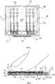
Fig. 1 schematically illustrates a configuration of a semiconductor fingerprint identification sensor in accordance with an embodiment of the invention; -
Fig. 2 schematically illustrates a cross-section view of a configuration of a semiconductor fingerprint identification sensor in accordance with an embodiment of the invention. - In order to make objects, technical details and advantages of the embodiments of the invention apparent, the technical solutions of the embodiments will be described in a clearly and fully understandable way in connection with the drawings related to the embodiments of the invention.
- As illustrated in
Fig. 1 , an embodiment of the present invention provides a semiconductor fingerprint identification sensor, which comprises: asensing area 1, acontrol area 2 and aninterface area 3; thesensing area 1, thecontrol area 2 and theinterface area 3 are communicated with one another; a fingerprint information sensed in thesensing area 1 is sent to thecontrol area 2, and is output through theinterface area 3 after the information is processed in thecontrol area 2. - As illustrated in
Fig. 2 , thesensing area 1 comprises aninsulation layer 50, a wiring layer 60, asubstrate layer 51 and aprotective layer 80 which are stacked in a sequence. The wiring layer 60 is embedded between theinsulation layer 50 and thesubstrate layer 51. Asensor array 11 is disposed on a side of thesubstrate layer 51 in contact with theprotective layer 80. A electrically conductive viahole 10 corresponding to thesensor array 11 is disposed on thesubstrate layer 51, and thesensor array 11 is electrically connected with asensing lead circuit 12 of the wiring layer 60 through thevia hole 10. The semiconductor fingerprint identification sensor is described in detail as below. - As an example of the present invention, both the
insulation layer 50 and thesubstrate layer 51 in thesensing area 1 are made from a flexible insulating material, such as polyimide or polyester film. Theprotective layer 80 is made from a material with a high dielectric constant and high hardness, such as Si3N4 or polytetrafluoroethene (PTFE), etc. For example, the high dielectric constant and high hardness material is deposited on a top surface of thesubstrate layer 51 by means of sputtering, evaporation or the like to form theprotective layer 80. For example, the thickness of theprotective layer 80 is less than 5µm. - For example, the
protective layer 80 is made from Si3N4, due to Si3N4 with high dielectric constant and ultra-thin thickness, the capacitance signal variation cannot be too small while the finger contacts thesensor array 11. Moreover, the reliability of the sensor is increased due to Si3N4 with good wear-resisting property. - The
sensor array 11 disposed in thesensing area 1 comprises a plurality of semiconductor sensor units which are arranged in an N×N array. The number of the semiconductor sensor unit per inch, for example, is more than 300, to ensure the identification accuracy. Thesensor array 11 is made from high conductivity material, such as copper and silver. As an example, thesensor array 11 is made from copper. The fingerprint information sensed in thesensor array 11 is sent to thecontrol area 2 through thevia hole 10 disposed on thesubstrate layer 51 and asensing lead circuit 12 disposed in the wiring layer 60. Every lead in the wiring layer 60 does not intersect each other, thus the parasitic capacitance is minimized. A printed circuit is used as thesensing lead circuit 12 in the wiring layer 60, for example, the material of the printed circuit is liquid silver. - As an example of the present invention, as illustrated in
Fig. 2 , thecontrol area 2 comprises aninsulation layer 50, a wiring layer 60 and asubstrate layer 51 which stacked in a sequence. The wiring layer 60 is embedded between theinsulation layer 50 and thesubstrate layer 51. A plurality ofbonding spots 21 are disposed on a side of thesubstrate layer 51 away from theinsulation layer 50, and a bonding pad is composed of the plurality ofbonding joints 21. Bonding pad viaholes 20 which correspond to thebonding joints 21 are disposed on thesubstrate layer 51, and thebonding joints 21 are electrically connected with asensing lead circuit 12 of the wiring layer 60 through the bonding pad viaholes 20. A fingerprint identification sensor integratedcircuit 22 is welded in thecontrol area 2. Fingerprint information collected in thesensing area 1 is identified and processed by the fingerprint identification sensor integratedcircuit 22 in thecontrol area 2 to become a fingerprint image, and then the image is output through theinterface area 3. A fingerprint identification sensor circuit comprises: thesensor array 11 and eachsensing lead circuit 12 of the wiring layer in thesensing area 1, and the fingerprint identification sensor integratedcircuit 22 in thecontrol area 2. - As illustrated in
Fig. 2 , theinterface area 3 comprises aninsulation layer 50, a wiring layer 60 and asubstrate layer 51 which stacked in a sequence. The wiring layer 60 is embedded between theinsulation layer 50 and thesubstrate layer 51. A plurality ofinterface contacts 31 are disposed on a side of thesubstrate layer 51 away from theinsulation layer 50. Interface viaholes 30 which correspond to theinterface contacts 31 are disposed on thesubstrate layer 51, and theinterface contacts 31 are electrically connected with asensing lead circuit 12 of the wiring layer 60 through the interface viaholes 30. - As illustrated in
Fig. 1 and Fig. 2 , thesensing area 1, thecontrol area 2 and theinterface area 3 may be integrally molded; theinsulation layer 50, the wiring layer 60 and thesubstrate layer 51 in thesensing area 1, thecontrol area 2 and theinterface area 3 may be made from the same material respectively. For example, thesensing area 1, thecontrol area 2 and theinterface area 3 are integrally molded to form an FPC (Flexible Printed Circuit board) together. - As illustrated in
Fig. 1 , the semiconductor fingerprint identification sensor further comprises an ESD (Electro-Static Discharge) loop 4, the ESD loop 4 surrounds thesensing area 1. In order to avoid the antenna loop effect, the ESD loop 4 is designed as segments, and the ESD loop 4 has anotch 42. The ESD loop 4 is made from a metal conductive material such as copper, nickel, or silver, etc. and wraps the whole sensor area, and is connected with an IC bonding pad. After the loop 4 is bonding to the IC, it is connected to the ground lead in the IC. In case static electricity is generated, it could be led to the ground by IC through the metallic conductor, and then the static is discharged, and that the damage and impact from static electricity on the sensor area is reduced. In addition, if the loop is a closed loop, the loop antenna effect will be caused, and then the detection of sensor signal is influenced. Hereby, the segment design is used, thenotch 42 is added, and the size of the notch is designed depending on the specific requirements, for example, the width of the notch is at least 30µm. - Another embodiment of the present invention provides a method for manufacturing the semiconductor fingerprint identification sensor, which comprises:
- cutting a flexible substrate, for example, the substrate in rolls is cut to a desired size according to the specific requirements;
- drilling a through hole on the flexible substrate by chemical etching or laser etc., metalizing the through hole (the metal is a high conductivity material such as cooper, or, silver, etc.) by chemical plating or carbon conductive layer electroplating to form an electrically conductive via hole, and a metal layer is also formed on a surface of the flexible substrate;
- cleansing the surface of the metal layer by chemical or mechanical method, forming a photosensitive film layer on the metal layer, and forming a sensing lead circuit of a wiring layer by a pattern process, for example, it is subjected to ultraviolet exposure, development by using developer, etching and peeling processes.
- coating an adhesive, such as polyimide, on the sensing lead circuit, forming an insulation layer after partially curing the adhesive, and linking the insulation layer with the wiring layer closely by hot-pressing and leaving no air bubbles;
- after cleansing a surface of the flexible substrate away from the wiring layer, electroplating a sensor array, an integrated circuit bonding pad (IC Bonding Pad) and an interface contact (also known as an interface golden finger) on the surface to form a sensing area, a control area and an interface area respectively; and
- forming a protective layer on a top surface of the flexible substrate, by depositing the high dielectric constant and high hardness material using sputtering, evaporation, etc. For example, the thickness of the protective layer is less than 5µm.
- after manufacturing the semiconductor fingerprint identification sensor, welding a sensor integrated circuit in the control area and testing the sensor.
- For example, punching and cutting a large flexible sensor into small pieces, reinforcing the control area with a reinforcement plate; coating ACF (Anisotropic Conductive Film) after cleansing the IC bonding pad; welding IC on the sensor after subjected to pre-bonding and bonding; finally performing lead check and testing electrical performance.
- According to the method for manufacturing the semiconductor fingerprint identification sensor provided in an embodiment of the present invention, the sensor pad is prepared on the flexible substrate, so the process cost is greatly reduced. IC is bonded on FPC, which is similar to COF (Chip on Film), and then the process is simplified and the process cost is greatly reduced.
- Embodiments of the present invention relate to a semiconductor fingerprint identification sensor and a method for manufacturing the same, a sensor array is prepared on a flexible substrate, in comparison with the traditional common semiconductor fingerprint sensor in which the sensor unit is prepared on a single crystal silicon substrate, the price competitiveness is enhanced by using cheaper flexible substrate. Further, the process is simplified by using IC bonding similar to COF. Because the flexible substrate is provided with metal wirings (which is made from high conductivity metal material, such as cooper, or silver, etc.), the signal loss is reduced and the signal-to-noise ratio is increased. The substrate is covered by the protective layer of the high dielectric constant material, in order to improve the sensor reliability. An ESD loop is designed for the semiconductor fingerprint identification sensor, in order to prevent the fingerprint signal from interference.
- What is described above is related to the illustrative embodiments of the disclosure only and not limitative to the scope of the disclosure; the scopes of the disclosure are defined by the accompanying claims.
- The present application claims the priority of Chinese patent application No.
201410317703.7 filed on July 4, 2014
Claims (10)
- A semiconductor fingerprint identification sensor, comprising:a sensing area (1), a control area (2) and an interface area (3), wherein the sensing area (1), the control area (2) and the interface area (3) are in communication with one another, and a fingerprint information sensed in the sensing area (1) is sent to the control area (2), and is output through the interface area (3) after being processed in the control area (2);the semiconductor fingerprint identification sensor further comprises:an insulation layer, a wiring layer, and a substrate layer, wherein the insulation layer, the wiring layer and the substrate layer are stacked in a sequence, the wiring layer is embedded between the insulation layer and the substrate layer and comprises a sensing lead circuit (12), each of the insulation layer, the wiring layer and the substrate layer is configured to extend across the sensing area, the control area and the interface area;wherein the sensing area (1) further comprises a protective layer (80), a sensor array (11), and an electrically conductive via hole (10), wherein the protective layer (80) is stacked on the substrate layer (51), the sensor array(11) is disposed on theside of the substrate layer (51) being in contact with the protective layer (80) and away from the insulation layer (50), the electrically conductive via hole (10) is formed in the substrate layer (51), and the sensor array (11) is configured to electrically connect with the sensing lead circuit (12) of the wiring layer (60) through the electrically conductive via hole (10);wherein the control area (2) comprises a fingerprint identification sensor integrated circuit (22), a bonding pad composed of a plurality of bonding joints (21), a plurality of bonding pad via holes (20), wherein the fingerprint identification sensor integrated circuit (22) is welded in the control area (2) and disposed on the same side of the substrate layer (51) as the sensor array (11), the plurality of bonding joints (21) are disposed on the side of the substrate layer (51) being away from the insulation layer (50), the plurality of bonding pad via holes (20) are formed in the substrate layer (51), the fingerprint identification sensor integrated circuit (22) is configured to electrically connect to the sensing lead circuit (12) of the wiring layer (60) through the bonding pad and the plurality of bonding pad via holes (20);wherein the interface area (3) comprises a plurality of interface contacts (31) and a plurality of interface via holes (30), wherein the plurality of interface contacts (31) are disposed on the side of the substrate layer (51) being away from the insulation layer (50), the plurality of interface via holes (30) are formed in the substrate layer (51), the plurality of interface contacts (31) is configured to electrically connect to the sensing lead circuit (12) of the wiring layer (60) through the plurality of interface via holes (30);wherein the sensor array (11) in the sensing area (1) is configured to sense the fingerprint information and to send the fingerprint information to the fingerprint identification sensor integrated circuit (22) in the control area (2) through the sensing lead circuit (12) of the wiring layer (60);wherein the fingerprint identification sensor integrated circuit (22) is configured to identify and process the fingerprint information sensed in the sensing area (1) so as to form a fingerprint image;wherein the interface area (3) is configured to output the fingerprint image.
- The semiconductor fingerprint identification sensor according to claim 1, wherein the insulation layer (50) and the substrate layer (51) are made from a flexible insulating material.
- The semiconductor fingerprint identification sensor according to claim 1, wherein the sensor array (11) is made from a high conductivity material.
- The semiconductor fingerprint identification sensor according to claim 1, wherein the protective layer (50) is made from a material with a high dielectric constant and high hardness.
- The semiconductor fingerprint identification sensor according to any one of claims 1-4, further comprising: an electro-static discharge loop (4), wherein the electro-static discharge loop (4) surrounds the sensing area (1).
- The semiconductor fingerprint identification sensor according to claim 5, wherein the electro-static discharge loop (4) comprises a notch (42).
- A method for manufacturing the semiconductor fingerprint identification sensor according to any one of claims 1-6, comprising:cutting a flexible substrate (51);drilling a through hole on the flexible substrate (51), and forming a metal layer on a surface of the flexible substrate (51), such that the electrically conductive via hole (10) is formed by metalizing the through hole;forming a photosensitive film layer on the metal layer, and forming a sensing lead circuit (12) of a wiring layer (60) by a pattern process;coating an insulation layer on the sensing lead circuit (12);electroplating a sensor array (11), an integrated circuit bonding pad and an interface contact (31) on a surface of the flexible substrate (51) away from the wiring layer (60) to form the sensing area (1), the control area (2) and the interface area (3) respectively; andforming a protective layer (60) on a top surface of the flexible substrate (51).
- The method for manufacturing the semiconductor fingerprint identification sensor according to claim 7, wherein the insulation layer (50) and the flexible substrate (51) are made from a flexible insulating material.
- The method for manufacturing the semiconductor fingerprint identification sensor according to claim 7, wherein the sensor array (11) is made from a high conductivity material.
- The method for manufacturing the semiconductor fingerprint identification sensor according to claim 7, wherein the protective layer (80) is made from a material with a high dielectric constant and high hardness.
Applications Claiming Priority (2)
| Application Number | Priority Date | Filing Date | Title |
|---|---|---|---|
| CN201410317703.7A CN104102902B (en) | 2014-07-04 | 2014-07-04 | A kind of semiconductor fingerprint identification sensor and its manufacture method |
| PCT/CN2014/091825 WO2016000389A1 (en) | 2014-07-04 | 2014-11-21 | Semiconductor fingerprint recognition sensor and manufacturing method therefor |
Publications (3)
| Publication Number | Publication Date |
|---|---|
| EP3168774A1 EP3168774A1 (en) | 2017-05-17 |
| EP3168774A4 EP3168774A4 (en) | 2018-01-03 |
| EP3168774B1 true EP3168774B1 (en) | 2020-10-28 |
Family
ID=51671042
Family Applications (1)
| Application Number | Title | Priority Date | Filing Date |
|---|---|---|---|
| EP14882773.6A Active EP3168774B1 (en) | 2014-07-04 | 2014-11-21 | Semiconductor fingerprint recognition sensor and manufacturing method therefor |
Country Status (4)
| Country | Link |
|---|---|
| US (1) | US10242242B2 (en) |
| EP (1) | EP3168774B1 (en) |
| CN (1) | CN104102902B (en) |
| WO (1) | WO2016000389A1 (en) |
Families Citing this family (33)
| Publication number | Priority date | Publication date | Assignee | Title |
|---|---|---|---|---|
| US8144319B2 (en) | 2009-05-07 | 2012-03-27 | Solum, Inc. | Automated soil measurement device |
| US9146223B1 (en) | 2012-08-03 | 2015-09-29 | Monsanto Technology Llc | Automated soil measurement device |
| US9291545B1 (en) | 2012-09-06 | 2016-03-22 | Monsanto Technology Llc | Self-filling soil processing chamber with dynamic extractant volume |
| CN104102902B (en) * | 2014-07-04 | 2017-07-04 | 京东方科技集团股份有限公司 | A kind of semiconductor fingerprint identification sensor and its manufacture method |
| CN105608406B (en) * | 2014-11-20 | 2019-05-28 | 上海箩箕技术有限公司 | Fingerprint sensor |
| CN104553113A (en) * | 2014-12-11 | 2015-04-29 | 业成光电(深圳)有限公司 | Acoustic wave fingerprint identification component and manufacturing method thereof |
| CN105893918A (en) * | 2015-01-26 | 2016-08-24 | 胡家安 | Fingerprint detection device and method |
| CN104751126A (en) * | 2015-03-06 | 2015-07-01 | 南昌欧菲生物识别技术有限公司 | Fingerprint identification device, touch screen and electronic equipment |
| CN104881628A (en) * | 2015-03-06 | 2015-09-02 | 南昌欧菲生物识别技术有限公司 | Fingerprint identification device, touch screen and electronic equipment |
| CN104751124A (en) * | 2015-03-06 | 2015-07-01 | 南昌欧菲生物识别技术有限公司 | Fingerprint identification device, touch screen and electronic equipment |
| TWI563253B (en) * | 2015-04-14 | 2016-12-21 | Lee Mei Yen | Composite substrate sensor device and method of manufacturing such sensor device |
| CN106292865B (en) * | 2015-06-24 | 2019-06-21 | 神盾股份有限公司 | electronic device |
| CN106326807B (en) * | 2015-06-24 | 2020-02-11 | 神盾股份有限公司 | Fingerprint sensor |
| CN106356348A (en) * | 2015-07-24 | 2017-01-25 | 晨星半导体股份有限公司 | Capacitive sensor structure, circuit board structure with capacitive sensor and packaging structure of capacitive sensor |
| CN106650552B (en) * | 2015-10-30 | 2019-09-13 | 深圳指芯智能科技有限公司 | A metal ring for fingerprint identification sensor and its preparation method and application |
| CN106767628B (en) * | 2015-12-18 | 2019-04-19 | 深圳市汇顶科技股份有限公司 | A kind of thickness detecting method and system of fingerprint sensor protective layer |
| TWI584202B (en) * | 2015-12-31 | 2017-05-21 | 速博思股份有限公司 | Fingerprint identification apparatus |
| US9792516B2 (en) * | 2016-01-26 | 2017-10-17 | Next Biometrics Group Asa | Flexible card with fingerprint sensor |
| TWI596716B (en) * | 2016-06-27 | 2017-08-21 | 速博思股份有限公司 | Fingerprint recognition apparatus |
| MY181171A (en) * | 2016-11-28 | 2020-12-21 | Carsem M Sdn Bhd | Low-profile electronic package |
| US10055637B2 (en) * | 2016-12-07 | 2018-08-21 | Synaptics Incorporated | Optical sensor with substrate light filter |
| EP3422397A4 (en) * | 2017-02-13 | 2019-07-31 | Shenzhen Goodix Technology Co., Ltd. | METHOD FOR SECONDARY ENCLOSURE OF INTERCONNECTION HOLE CHIP THROUGH SILICON AND ITS SECONDARY HOUSING |
| CN106980835B (en) * | 2017-03-24 | 2018-08-17 | 维沃移动通信有限公司 | A kind of fingerprint identification device and electronic equipment |
| TWI718365B (en) * | 2017-05-09 | 2021-02-11 | 漢辰科技股份有限公司 | Wafer charges monitoring |
| CN107564899A (en) * | 2017-08-22 | 2018-01-09 | 苏州科阳光电科技有限公司 | The method for packing and bio-identification module of a kind of bio-identification chip |
| CN110739327B (en) * | 2018-07-20 | 2022-06-07 | 京东方科技集团股份有限公司 | Array substrate, manufacturing method thereof and display device |
| CN112580389B (en) * | 2019-09-27 | 2024-05-10 | 速博思股份有限公司 | Fingerprint detection device |
| CN111126351B (en) * | 2020-01-21 | 2024-02-09 | 北京京东方光电科技有限公司 | Fingerprint recognition module |
| CN111987085B (en) * | 2020-08-21 | 2022-08-05 | 上海天马微电子有限公司 | Sensor, preparation method of sensor and electronic equipment |
| US11816919B2 (en) | 2021-06-04 | 2023-11-14 | Synaptics Incorporated | Sensor device for transcapacitive sensing with shielding |
| US11519801B1 (en) * | 2021-06-04 | 2022-12-06 | Synaptics Incorporated | Sensor device for transcapacitive sensing with shielding |
| TWI793030B (en) * | 2022-06-02 | 2023-02-11 | 義隆電子股份有限公司 | Card having a fingerprint sensor and manufacturing method of the same |
| EP4715764A1 (en) * | 2023-06-30 | 2026-03-25 | Samsung Electronics Co., Ltd. | Electronic device including fingerprint sensor |
Family Cites Families (13)
| Publication number | Priority date | Publication date | Assignee | Title |
|---|---|---|---|---|
| NO315017B1 (en) | 2000-06-09 | 2003-06-23 | Idex Asa | Sensor chip, especially for measuring structures in a finger surface |
| JP3806044B2 (en) * | 2002-02-08 | 2006-08-09 | 日本電信電話株式会社 | Surface shape recognition sensor and manufacturing method thereof |
| JP3684233B2 (en) * | 2002-05-14 | 2005-08-17 | キヤノン株式会社 | Fingerprint input device and manufacturing method thereof |
| CZ2005209A3 (en) * | 2002-09-10 | 2005-12-14 | Ivi Smart Technologies, Inc. | Secure Biometric Identity Verification |
| JP4160851B2 (en) | 2003-03-31 | 2008-10-08 | 富士通株式会社 | Semiconductor device for fingerprint recognition |
| TWI224191B (en) * | 2003-05-28 | 2004-11-21 | Au Optronics Corp | Capacitive semiconductor pressure sensor |
| NO20083766L (en) | 2008-09-01 | 2010-03-02 | Idex Asa | surface Sensor |
| US8716613B2 (en) | 2010-03-02 | 2014-05-06 | Synaptics Incoporated | Apparatus and method for electrostatic discharge protection |
| CA2892181C (en) * | 2012-11-22 | 2020-03-31 | Universite Laval | Electrochemical sensor |
| CN203232406U (en) | 2013-05-15 | 2013-10-09 | 京东方科技集团股份有限公司 | Capacitive touch screen and display device |
| CN103294312B (en) | 2013-05-15 | 2016-04-20 | 京东方科技集团股份有限公司 | Capacitive touch screen, capacitive touch screen preparation method and display device |
| CN203366350U (en) * | 2013-07-24 | 2013-12-25 | 江苏恒成高科信息科技有限公司 | Fingerprint reading sensor ic card |
| CN104102902B (en) | 2014-07-04 | 2017-07-04 | 京东方科技集团股份有限公司 | A kind of semiconductor fingerprint identification sensor and its manufacture method |
-
2014
- 2014-07-04 CN CN201410317703.7A patent/CN104102902B/en not_active Expired - Fee Related
- 2014-11-21 EP EP14882773.6A patent/EP3168774B1/en active Active
- 2014-11-21 WO PCT/CN2014/091825 patent/WO2016000389A1/en not_active Ceased
- 2014-11-21 US US14/762,847 patent/US10242242B2/en active Active
Non-Patent Citations (1)
| Title |
|---|
| None * |
Also Published As
| Publication number | Publication date |
|---|---|
| WO2016000389A1 (en) | 2016-01-07 |
| US20160247009A1 (en) | 2016-08-25 |
| CN104102902A (en) | 2014-10-15 |
| EP3168774A1 (en) | 2017-05-17 |
| CN104102902B (en) | 2017-07-04 |
| EP3168774A4 (en) | 2018-01-03 |
| US10242242B2 (en) | 2019-03-26 |
Similar Documents
| Publication | Publication Date | Title |
|---|---|---|
| US10242242B2 (en) | Semiconductor fingerprint identification sensor and manufacturing method thereof | |
| CN105404880B (en) | Electronic device with fingerprint sensor assembly | |
| JP5753857B2 (en) | Surface sensor | |
| CN203608443U (en) | Printed circuit and electronic module provided with same | |
| US20200225098A1 (en) | Force sensor and manufacturing method thereof | |
| WO2010032602A1 (en) | Semiconductor device | |
| CN115000135B (en) | Display substrate and preparation method thereof, and display module | |
| US11081436B2 (en) | Component carrier with integrated strain gauge | |
| CN107381494A (en) | Fingerprint sensor and packaging method thereof | |
| KR20190089406A (en) | Fingerprint sensing module and lectronic device comprising the same | |
| CN115988949A (en) | Electronic equipment, ultrasonic transducer and its semiconductor chip, and manufacturing method | |
| JP2018194483A (en) | Sensor unit and sensor module | |
| US12320718B2 (en) | Pressure sensing circuit board and method for manufacturing the same | |
| US7768459B2 (en) | Transponder card | |
| US10095330B2 (en) | Printed wiring board | |
| KR20140142936A (en) | Flexible printed circuit board and the manufacturing method | |
| KR100854104B1 (en) | Electrical connection member for RDF tag manufacturing method, RDF tag and RDF tag | |
| CN116978077B (en) | Ultrasonic fingerprint recognition device and electronic device | |
| US20250207986A1 (en) | Pressure sensing flexible circuit board and method of fabricating the same | |
| CN121397858A (en) | Flexible circuit board, circuit board assembly, temperature detection device and electronic equipment | |
| CN115357133A (en) | Touch module and touch display panel | |
| KR101551733B1 (en) | Conductive film for forming touch panel and touch panel manufactured by using the same | |
| JP2018197942A (en) | IC card with non-contact communication function | |
| KR20170135118A (en) | Touch force sensing apparatus | |
| JP2017027543A (en) | Inlay for non-contact type information medium |
Legal Events
| Date | Code | Title | Description |
|---|---|---|---|
| PUAI | Public reference made under article 153(3) epc to a published international application that has entered the european phase |
Free format text: ORIGINAL CODE: 0009012 |
|
| STAA | Information on the status of an ep patent application or granted ep patent |
Free format text: STATUS: REQUEST FOR EXAMINATION WAS MADE |
|
| 17P | Request for examination filed |
Effective date: 20150821 |
|
| AK | Designated contracting states |
Kind code of ref document: A1 Designated state(s): AL AT BE BG CH CY CZ DE DK EE ES FI FR GB GR HR HU IE IS IT LI LT LU LV MC MK MT NL NO PL PT RO RS SE SI SK SM TR |
|
| AX | Request for extension of the european patent |
Extension state: BA ME |
|
| DAX | Request for extension of the european patent (deleted) | ||
| A4 | Supplementary search report drawn up and despatched |
Effective date: 20171130 |
|
| RIC1 | Information provided on ipc code assigned before grant |
Ipc: G06K 9/00 20060101AFI20171124BHEP |
|
| STAA | Information on the status of an ep patent application or granted ep patent |
Free format text: STATUS: EXAMINATION IS IN PROGRESS |
|
| 17Q | First examination report despatched |
Effective date: 20190621 |
|
| GRAP | Despatch of communication of intention to grant a patent |
Free format text: ORIGINAL CODE: EPIDOSNIGR1 |
|
| STAA | Information on the status of an ep patent application or granted ep patent |
Free format text: STATUS: GRANT OF PATENT IS INTENDED |
|
| RIC1 | Information provided on ipc code assigned before grant |
Ipc: H01L 23/31 20060101ALN20200422BHEP Ipc: G06K 9/00 20060101AFI20200422BHEP |
|
| INTG | Intention to grant announced |
Effective date: 20200527 |
|
| GRAS | Grant fee paid |
Free format text: ORIGINAL CODE: EPIDOSNIGR3 |
|
| GRAA | (expected) grant |
Free format text: ORIGINAL CODE: 0009210 |
|
| STAA | Information on the status of an ep patent application or granted ep patent |
Free format text: STATUS: THE PATENT HAS BEEN GRANTED |
|
| AK | Designated contracting states |
Kind code of ref document: B1 Designated state(s): AL AT BE BG CH CY CZ DE DK EE ES FI FR GB GR HR HU IE IS IT LI LT LU LV MC MK MT NL NO PL PT RO RS SE SI SK SM TR |
|
| REG | Reference to a national code |
Ref country code: GB Ref legal event code: FG4D |
|
| REG | Reference to a national code |
Ref country code: CH Ref legal event code: EP |
|
| REG | Reference to a national code |
Ref country code: DE Ref legal event code: R096 Ref document number: 602014071832 Country of ref document: DE |
|
| REG | Reference to a national code |
Ref country code: AT Ref legal event code: REF Ref document number: 1328946 Country of ref document: AT Kind code of ref document: T Effective date: 20201115 |
|
| REG | Reference to a national code |
Ref country code: IE Ref legal event code: FG4D |
|
| REG | Reference to a national code |
Ref country code: AT Ref legal event code: MK05 Ref document number: 1328946 Country of ref document: AT Kind code of ref document: T Effective date: 20201028 |
|
| REG | Reference to a national code |
Ref country code: NL Ref legal event code: MP Effective date: 20201028 |
|
| PG25 | Lapsed in a contracting state [announced via postgrant information from national office to epo] |
Ref country code: GR Free format text: LAPSE BECAUSE OF FAILURE TO SUBMIT A TRANSLATION OF THE DESCRIPTION OR TO PAY THE FEE WITHIN THE PRESCRIBED TIME-LIMIT Effective date: 20210129 Ref country code: NO Free format text: LAPSE BECAUSE OF FAILURE TO SUBMIT A TRANSLATION OF THE DESCRIPTION OR TO PAY THE FEE WITHIN THE PRESCRIBED TIME-LIMIT Effective date: 20210128 Ref country code: NL Free format text: LAPSE BECAUSE OF FAILURE TO SUBMIT A TRANSLATION OF THE DESCRIPTION OR TO PAY THE FEE WITHIN THE PRESCRIBED TIME-LIMIT Effective date: 20201028 Ref country code: PT Free format text: LAPSE BECAUSE OF FAILURE TO SUBMIT A TRANSLATION OF THE DESCRIPTION OR TO PAY THE FEE WITHIN THE PRESCRIBED TIME-LIMIT Effective date: 20210301 Ref country code: FI Free format text: LAPSE BECAUSE OF FAILURE TO SUBMIT A TRANSLATION OF THE DESCRIPTION OR TO PAY THE FEE WITHIN THE PRESCRIBED TIME-LIMIT Effective date: 20201028 Ref country code: RS Free format text: LAPSE BECAUSE OF FAILURE TO SUBMIT A TRANSLATION OF THE DESCRIPTION OR TO PAY THE FEE WITHIN THE PRESCRIBED TIME-LIMIT Effective date: 20201028 |
|
| REG | Reference to a national code |
Ref country code: LT Ref legal event code: MG4D |
|
| PG25 | Lapsed in a contracting state [announced via postgrant information from national office to epo] |
Ref country code: ES Free format text: LAPSE BECAUSE OF FAILURE TO SUBMIT A TRANSLATION OF THE DESCRIPTION OR TO PAY THE FEE WITHIN THE PRESCRIBED TIME-LIMIT Effective date: 20201028 Ref country code: AT Free format text: LAPSE BECAUSE OF FAILURE TO SUBMIT A TRANSLATION OF THE DESCRIPTION OR TO PAY THE FEE WITHIN THE PRESCRIBED TIME-LIMIT Effective date: 20201028 Ref country code: BG Free format text: LAPSE BECAUSE OF FAILURE TO SUBMIT A TRANSLATION OF THE DESCRIPTION OR TO PAY THE FEE WITHIN THE PRESCRIBED TIME-LIMIT Effective date: 20210128 Ref country code: PL Free format text: LAPSE BECAUSE OF FAILURE TO SUBMIT A TRANSLATION OF THE DESCRIPTION OR TO PAY THE FEE WITHIN THE PRESCRIBED TIME-LIMIT Effective date: 20201028 Ref country code: SE Free format text: LAPSE BECAUSE OF FAILURE TO SUBMIT A TRANSLATION OF THE DESCRIPTION OR TO PAY THE FEE WITHIN THE PRESCRIBED TIME-LIMIT Effective date: 20201028 Ref country code: LV Free format text: LAPSE BECAUSE OF FAILURE TO SUBMIT A TRANSLATION OF THE DESCRIPTION OR TO PAY THE FEE WITHIN THE PRESCRIBED TIME-LIMIT Effective date: 20201028 Ref country code: IS Free format text: LAPSE BECAUSE OF FAILURE TO SUBMIT A TRANSLATION OF THE DESCRIPTION OR TO PAY THE FEE WITHIN THE PRESCRIBED TIME-LIMIT Effective date: 20210228 |
|
| PG25 | Lapsed in a contracting state [announced via postgrant information from national office to epo] |
Ref country code: HR Free format text: LAPSE BECAUSE OF FAILURE TO SUBMIT A TRANSLATION OF THE DESCRIPTION OR TO PAY THE FEE WITHIN THE PRESCRIBED TIME-LIMIT Effective date: 20201028 |
|
| REG | Reference to a national code |
Ref country code: CH Ref legal event code: PL |
|
| REG | Reference to a national code |
Ref country code: DE Ref legal event code: R097 Ref document number: 602014071832 Country of ref document: DE |
|
| PG25 | Lapsed in a contracting state [announced via postgrant information from national office to epo] |
Ref country code: EE Free format text: LAPSE BECAUSE OF FAILURE TO SUBMIT A TRANSLATION OF THE DESCRIPTION OR TO PAY THE FEE WITHIN THE PRESCRIBED TIME-LIMIT Effective date: 20201028 Ref country code: CZ Free format text: LAPSE BECAUSE OF FAILURE TO SUBMIT A TRANSLATION OF THE DESCRIPTION OR TO PAY THE FEE WITHIN THE PRESCRIBED TIME-LIMIT Effective date: 20201028 Ref country code: SM Free format text: LAPSE BECAUSE OF FAILURE TO SUBMIT A TRANSLATION OF THE DESCRIPTION OR TO PAY THE FEE WITHIN THE PRESCRIBED TIME-LIMIT Effective date: 20201028 Ref country code: MC Free format text: LAPSE BECAUSE OF FAILURE TO SUBMIT A TRANSLATION OF THE DESCRIPTION OR TO PAY THE FEE WITHIN THE PRESCRIBED TIME-LIMIT Effective date: 20201028 Ref country code: LU Free format text: LAPSE BECAUSE OF NON-PAYMENT OF DUE FEES Effective date: 20201121 Ref country code: LT Free format text: LAPSE BECAUSE OF FAILURE TO SUBMIT A TRANSLATION OF THE DESCRIPTION OR TO PAY THE FEE WITHIN THE PRESCRIBED TIME-LIMIT Effective date: 20201028 Ref country code: SK Free format text: LAPSE BECAUSE OF FAILURE TO SUBMIT A TRANSLATION OF THE DESCRIPTION OR TO PAY THE FEE WITHIN THE PRESCRIBED TIME-LIMIT Effective date: 20201028 Ref country code: RO Free format text: LAPSE BECAUSE OF FAILURE TO SUBMIT A TRANSLATION OF THE DESCRIPTION OR TO PAY THE FEE WITHIN THE PRESCRIBED TIME-LIMIT Effective date: 20201028 |
|
| REG | Reference to a national code |
Ref country code: BE Ref legal event code: MM Effective date: 20201130 |
|
| PG25 | Lapsed in a contracting state [announced via postgrant information from national office to epo] |
Ref country code: CH Free format text: LAPSE BECAUSE OF NON-PAYMENT OF DUE FEES Effective date: 20201130 Ref country code: DK Free format text: LAPSE BECAUSE OF FAILURE TO SUBMIT A TRANSLATION OF THE DESCRIPTION OR TO PAY THE FEE WITHIN THE PRESCRIBED TIME-LIMIT Effective date: 20201028 Ref country code: LI Free format text: LAPSE BECAUSE OF NON-PAYMENT OF DUE FEES Effective date: 20201130 |
|
| PLBE | No opposition filed within time limit |
Free format text: ORIGINAL CODE: 0009261 |
|
| STAA | Information on the status of an ep patent application or granted ep patent |
Free format text: STATUS: NO OPPOSITION FILED WITHIN TIME LIMIT |
|
| 26N | No opposition filed |
Effective date: 20210729 |
|
| PG25 | Lapsed in a contracting state [announced via postgrant information from national office to epo] |
Ref country code: IE Free format text: LAPSE BECAUSE OF NON-PAYMENT OF DUE FEES Effective date: 20201121 Ref country code: IT Free format text: LAPSE BECAUSE OF FAILURE TO SUBMIT A TRANSLATION OF THE DESCRIPTION OR TO PAY THE FEE WITHIN THE PRESCRIBED TIME-LIMIT Effective date: 20201028 Ref country code: AL Free format text: LAPSE BECAUSE OF FAILURE TO SUBMIT A TRANSLATION OF THE DESCRIPTION OR TO PAY THE FEE WITHIN THE PRESCRIBED TIME-LIMIT Effective date: 20201028 |
|
| REG | Reference to a national code |
Ref country code: DE Ref legal event code: R079 Ref document number: 602014071832 Country of ref document: DE Free format text: PREVIOUS MAIN CLASS: G06K0009000000 Ipc: G06V0010000000 |
|
| PG25 | Lapsed in a contracting state [announced via postgrant information from national office to epo] |
Ref country code: SI Free format text: LAPSE BECAUSE OF FAILURE TO SUBMIT A TRANSLATION OF THE DESCRIPTION OR TO PAY THE FEE WITHIN THE PRESCRIBED TIME-LIMIT Effective date: 20201028 |
|
| PG25 | Lapsed in a contracting state [announced via postgrant information from national office to epo] |
Ref country code: IS Free format text: LAPSE BECAUSE OF FAILURE TO SUBMIT A TRANSLATION OF THE DESCRIPTION OR TO PAY THE FEE WITHIN THE PRESCRIBED TIME-LIMIT Effective date: 20210228 Ref country code: TR Free format text: LAPSE BECAUSE OF FAILURE TO SUBMIT A TRANSLATION OF THE DESCRIPTION OR TO PAY THE FEE WITHIN THE PRESCRIBED TIME-LIMIT Effective date: 20201028 Ref country code: MT Free format text: LAPSE BECAUSE OF FAILURE TO SUBMIT A TRANSLATION OF THE DESCRIPTION OR TO PAY THE FEE WITHIN THE PRESCRIBED TIME-LIMIT Effective date: 20201028 Ref country code: CY Free format text: LAPSE BECAUSE OF FAILURE TO SUBMIT A TRANSLATION OF THE DESCRIPTION OR TO PAY THE FEE WITHIN THE PRESCRIBED TIME-LIMIT Effective date: 20201028 |
|
| PG25 | Lapsed in a contracting state [announced via postgrant information from national office to epo] |
Ref country code: MK Free format text: LAPSE BECAUSE OF FAILURE TO SUBMIT A TRANSLATION OF THE DESCRIPTION OR TO PAY THE FEE WITHIN THE PRESCRIBED TIME-LIMIT Effective date: 20201028 |
|
| PG25 | Lapsed in a contracting state [announced via postgrant information from national office to epo] |
Ref country code: BE Free format text: LAPSE BECAUSE OF NON-PAYMENT OF DUE FEES Effective date: 20201130 |
|
| P01 | Opt-out of the competence of the unified patent court (upc) registered |
Effective date: 20230630 |
|
| PGFP | Annual fee paid to national office [announced via postgrant information from national office to epo] |
Ref country code: GB Payment date: 20231026 Year of fee payment: 10 |
|
| PGFP | Annual fee paid to national office [announced via postgrant information from national office to epo] |
Ref country code: FR Payment date: 20231011 Year of fee payment: 10 Ref country code: DE Payment date: 20231120 Year of fee payment: 10 |
|
| REG | Reference to a national code |
Ref country code: DE Ref legal event code: R119 Ref document number: 602014071832 Country of ref document: DE |
|
| GBPC | Gb: european patent ceased through non-payment of renewal fee |
Effective date: 20241121 |
|
| PG25 | Lapsed in a contracting state [announced via postgrant information from national office to epo] |
Ref country code: DE Free format text: LAPSE BECAUSE OF NON-PAYMENT OF DUE FEES Effective date: 20250603 |
|
| PG25 | Lapsed in a contracting state [announced via postgrant information from national office to epo] |
Ref country code: GB Free format text: LAPSE BECAUSE OF NON-PAYMENT OF DUE FEES Effective date: 20241121 |
|
| PG25 | Lapsed in a contracting state [announced via postgrant information from national office to epo] |
Ref country code: FR Free format text: LAPSE BECAUSE OF NON-PAYMENT OF DUE FEES Effective date: 20241130 |