EP3165583A1 - Bonding method, method for manufacturing structure, and structure - Google Patents
Bonding method, method for manufacturing structure, and structure Download PDFInfo
- Publication number
- EP3165583A1 EP3165583A1 EP15814156.4A EP15814156A EP3165583A1 EP 3165583 A1 EP3165583 A1 EP 3165583A1 EP 15814156 A EP15814156 A EP 15814156A EP 3165583 A1 EP3165583 A1 EP 3165583A1
- Authority
- EP
- European Patent Office
- Prior art keywords
- region
- bonding
- thin film
- specific region
- gold
- Prior art date
- Legal status (The legal status is an assumption and is not a legal conclusion. Google has not performed a legal analysis and makes no representation as to the accuracy of the status listed.)
- Granted
Links
Images


Classifications
-
- B—PERFORMING OPERATIONS; TRANSPORTING
- B32—LAYERED PRODUCTS
- B32B—LAYERED PRODUCTS, i.e. PRODUCTS BUILT-UP OF STRATA OF FLAT OR NON-FLAT, e.g. CELLULAR OR HONEYCOMB, FORM
- B32B15/00—Layered products comprising a layer of metal
- B32B15/04—Layered products comprising a layer of metal comprising metal as the main or only constituent of a layer, which is next to another layer of the same or of a different material
-
- B—PERFORMING OPERATIONS; TRANSPORTING
- B32—LAYERED PRODUCTS
- B32B—LAYERED PRODUCTS, i.e. PRODUCTS BUILT-UP OF STRATA OF FLAT OR NON-FLAT, e.g. CELLULAR OR HONEYCOMB, FORM
- B32B15/00—Layered products comprising a layer of metal
- B32B15/20—Layered products comprising a layer of metal comprising aluminium or copper
-
- B—PERFORMING OPERATIONS; TRANSPORTING
- B32—LAYERED PRODUCTS
- B32B—LAYERED PRODUCTS, i.e. PRODUCTS BUILT-UP OF STRATA OF FLAT OR NON-FLAT, e.g. CELLULAR OR HONEYCOMB, FORM
- B32B17/00—Layered products essentially comprising sheet glass, or glass, slag, or like fibres
-
- B—PERFORMING OPERATIONS; TRANSPORTING
- B32—LAYERED PRODUCTS
- B32B—LAYERED PRODUCTS, i.e. PRODUCTS BUILT-UP OF STRATA OF FLAT OR NON-FLAT, e.g. CELLULAR OR HONEYCOMB, FORM
- B32B37/00—Methods or apparatus for laminating, e.g. by curing or by ultrasonic bonding
- B32B37/12—Methods or apparatus for laminating, e.g. by curing or by ultrasonic bonding characterised by using adhesives
-
- B—PERFORMING OPERATIONS; TRANSPORTING
- B32—LAYERED PRODUCTS
- B32B—LAYERED PRODUCTS, i.e. PRODUCTS BUILT-UP OF STRATA OF FLAT OR NON-FLAT, e.g. CELLULAR OR HONEYCOMB, FORM
- B32B38/00—Ancillary operations in connection with laminating processes
- B32B38/0008—Electrical discharge treatment, e.g. corona, plasma treatment; wave energy or particle radiation
-
- B—PERFORMING OPERATIONS; TRANSPORTING
- B32—LAYERED PRODUCTS
- B32B—LAYERED PRODUCTS, i.e. PRODUCTS BUILT-UP OF STRATA OF FLAT OR NON-FLAT, e.g. CELLULAR OR HONEYCOMB, FORM
- B32B7/00—Layered products characterised by the relation between layers; Layered products characterised by the relative orientation of features between layers, or by the relative values of a measurable parameter between layers, i.e. products comprising layers having different physical, chemical or physicochemical properties; Layered products characterised by the interconnection of layers
- B32B7/04—Interconnection of layers
- B32B7/12—Interconnection of layers using interposed adhesives or interposed materials with bonding properties
-
- C—CHEMISTRY; METALLURGY
- C03—GLASS; MINERAL OR SLAG WOOL
- C03C—CHEMICAL COMPOSITION OF GLASSES, GLAZES OR VITREOUS ENAMELS; SURFACE TREATMENT OF GLASS; SURFACE TREATMENT OF FIBRES OR FILAMENTS MADE FROM GLASS, MINERALS OR SLAGS; JOINING GLASS TO GLASS OR OTHER MATERIALS
- C03C27/00—Joining pieces of glass to pieces of other inorganic material; Joining glass to glass other than by fusing
- C03C27/04—Joining glass to metal by means of an interlayer
- C03C27/048—Joining glass to metal by means of an interlayer consisting of an adhesive specially adapted for that purpose
-
- C—CHEMISTRY; METALLURGY
- C09—DYES; PAINTS; POLISHES; NATURAL RESINS; ADHESIVES; COMPOSITIONS NOT OTHERWISE PROVIDED FOR; APPLICATIONS OF MATERIALS NOT OTHERWISE PROVIDED FOR
- C09J—ADHESIVES; NON-MECHANICAL ASPECTS OF ADHESIVE PROCESSES IN GENERAL; ADHESIVE PROCESSES NOT PROVIDED FOR ELSEWHERE; USE OF MATERIALS AS ADHESIVES
- C09J201/00—Adhesives based on unspecified macromolecular compounds
-
- C—CHEMISTRY; METALLURGY
- C09—DYES; PAINTS; POLISHES; NATURAL RESINS; ADHESIVES; COMPOSITIONS NOT OTHERWISE PROVIDED FOR; APPLICATIONS OF MATERIALS NOT OTHERWISE PROVIDED FOR
- C09J—ADHESIVES; NON-MECHANICAL ASPECTS OF ADHESIVE PROCESSES IN GENERAL; ADHESIVE PROCESSES NOT PROVIDED FOR ELSEWHERE; USE OF MATERIALS AS ADHESIVES
- C09J5/00—Adhesive processes in general; Adhesive processes not provided for elsewhere, e.g. relating to primers
- C09J5/02—Adhesive processes in general; Adhesive processes not provided for elsewhere, e.g. relating to primers involving pretreatment of the surfaces to be joined
-
- B—PERFORMING OPERATIONS; TRANSPORTING
- B32—LAYERED PRODUCTS
- B32B—LAYERED PRODUCTS, i.e. PRODUCTS BUILT-UP OF STRATA OF FLAT OR NON-FLAT, e.g. CELLULAR OR HONEYCOMB, FORM
- B32B2250/00—Layers arrangement
- B32B2250/02—2 layers
-
- B—PERFORMING OPERATIONS; TRANSPORTING
- B32—LAYERED PRODUCTS
- B32B—LAYERED PRODUCTS, i.e. PRODUCTS BUILT-UP OF STRATA OF FLAT OR NON-FLAT, e.g. CELLULAR OR HONEYCOMB, FORM
- B32B2250/00—Layers arrangement
- B32B2250/44—Number of layers variable across the laminate
-
- B—PERFORMING OPERATIONS; TRANSPORTING
- B32—LAYERED PRODUCTS
- B32B—LAYERED PRODUCTS, i.e. PRODUCTS BUILT-UP OF STRATA OF FLAT OR NON-FLAT, e.g. CELLULAR OR HONEYCOMB, FORM
- B32B2255/00—Coating on the layer surface
- B32B2255/06—Coating on the layer surface on metal layer
-
- B—PERFORMING OPERATIONS; TRANSPORTING
- B32—LAYERED PRODUCTS
- B32B—LAYERED PRODUCTS, i.e. PRODUCTS BUILT-UP OF STRATA OF FLAT OR NON-FLAT, e.g. CELLULAR OR HONEYCOMB, FORM
- B32B2255/00—Coating on the layer surface
- B32B2255/20—Inorganic coating
- B32B2255/205—Metallic coating
-
- B—PERFORMING OPERATIONS; TRANSPORTING
- B32—LAYERED PRODUCTS
- B32B—LAYERED PRODUCTS, i.e. PRODUCTS BUILT-UP OF STRATA OF FLAT OR NON-FLAT, e.g. CELLULAR OR HONEYCOMB, FORM
- B32B2255/00—Coating on the layer surface
- B32B2255/28—Multiple coating on one surface
-
- B—PERFORMING OPERATIONS; TRANSPORTING
- B32—LAYERED PRODUCTS
- B32B—LAYERED PRODUCTS, i.e. PRODUCTS BUILT-UP OF STRATA OF FLAT OR NON-FLAT, e.g. CELLULAR OR HONEYCOMB, FORM
- B32B2307/00—Properties of the layers or laminate
- B32B2307/40—Properties of the layers or laminate having particular optical properties
- B32B2307/412—Transparent
-
- B—PERFORMING OPERATIONS; TRANSPORTING
- B32—LAYERED PRODUCTS
- B32B—LAYERED PRODUCTS, i.e. PRODUCTS BUILT-UP OF STRATA OF FLAT OR NON-FLAT, e.g. CELLULAR OR HONEYCOMB, FORM
- B32B2307/00—Properties of the layers or laminate
- B32B2307/50—Properties of the layers or laminate having particular mechanical properties
-
- B—PERFORMING OPERATIONS; TRANSPORTING
- B32—LAYERED PRODUCTS
- B32B—LAYERED PRODUCTS, i.e. PRODUCTS BUILT-UP OF STRATA OF FLAT OR NON-FLAT, e.g. CELLULAR OR HONEYCOMB, FORM
- B32B2307/00—Properties of the layers or laminate
- B32B2307/50—Properties of the layers or laminate having particular mechanical properties
- B32B2307/538—Roughness
-
- B—PERFORMING OPERATIONS; TRANSPORTING
- B32—LAYERED PRODUCTS
- B32B—LAYERED PRODUCTS, i.e. PRODUCTS BUILT-UP OF STRATA OF FLAT OR NON-FLAT, e.g. CELLULAR OR HONEYCOMB, FORM
- B32B2307/00—Properties of the layers or laminate
- B32B2307/70—Other properties
- B32B2307/732—Dimensional properties
-
- B—PERFORMING OPERATIONS; TRANSPORTING
- B32—LAYERED PRODUCTS
- B32B—LAYERED PRODUCTS, i.e. PRODUCTS BUILT-UP OF STRATA OF FLAT OR NON-FLAT, e.g. CELLULAR OR HONEYCOMB, FORM
- B32B2457/00—Electrical equipment
-
- B—PERFORMING OPERATIONS; TRANSPORTING
- B32—LAYERED PRODUCTS
- B32B—LAYERED PRODUCTS, i.e. PRODUCTS BUILT-UP OF STRATA OF FLAT OR NON-FLAT, e.g. CELLULAR OR HONEYCOMB, FORM
- B32B2551/00—Optical elements
-
- C—CHEMISTRY; METALLURGY
- C09—DYES; PAINTS; POLISHES; NATURAL RESINS; ADHESIVES; COMPOSITIONS NOT OTHERWISE PROVIDED FOR; APPLICATIONS OF MATERIALS NOT OTHERWISE PROVIDED FOR
- C09J—ADHESIVES; NON-MECHANICAL ASPECTS OF ADHESIVE PROCESSES IN GENERAL; ADHESIVE PROCESSES NOT PROVIDED FOR ELSEWHERE; USE OF MATERIALS AS ADHESIVES
- C09J2301/00—Additional features of adhesives in the form of films or foils
- C09J2301/40—Additional features of adhesives in the form of films or foils characterized by the presence of essential components
- C09J2301/416—Additional features of adhesives in the form of films or foils characterized by the presence of essential components use of irradiation
-
- C—CHEMISTRY; METALLURGY
- C09—DYES; PAINTS; POLISHES; NATURAL RESINS; ADHESIVES; COMPOSITIONS NOT OTHERWISE PROVIDED FOR; APPLICATIONS OF MATERIALS NOT OTHERWISE PROVIDED FOR
- C09J—ADHESIVES; NON-MECHANICAL ASPECTS OF ADHESIVE PROCESSES IN GENERAL; ADHESIVE PROCESSES NOT PROVIDED FOR ELSEWHERE; USE OF MATERIALS AS ADHESIVES
- C09J2400/00—Presence of inorganic and organic materials
- C09J2400/10—Presence of inorganic materials
- C09J2400/16—Metal
- C09J2400/163—Metal in the substrate
-
- C—CHEMISTRY; METALLURGY
- C09—DYES; PAINTS; POLISHES; NATURAL RESINS; ADHESIVES; COMPOSITIONS NOT OTHERWISE PROVIDED FOR; APPLICATIONS OF MATERIALS NOT OTHERWISE PROVIDED FOR
- C09J—ADHESIVES; NON-MECHANICAL ASPECTS OF ADHESIVE PROCESSES IN GENERAL; ADHESIVE PROCESSES NOT PROVIDED FOR ELSEWHERE; USE OF MATERIALS AS ADHESIVES
- C09J2400/00—Presence of inorganic and organic materials
- C09J2400/10—Presence of inorganic materials
- C09J2400/16—Metal
- C09J2400/166—Metal in the pretreated surface to be joined
-
- H—ELECTRICITY
- H10—SEMICONDUCTOR DEVICES; ELECTRIC SOLID-STATE DEVICES NOT OTHERWISE PROVIDED FOR
- H10W—GENERIC PACKAGES, INTERCONNECTIONS, CONNECTORS OR OTHER CONSTRUCTIONAL DETAILS OF DEVICES COVERED BY CLASS H10
- H10W72/00—Interconnections or connectors in packages
- H10W72/01—Manufacture or treatment
- H10W72/013—Manufacture or treatment of die-attach connectors
- H10W72/01371—Cleaning, e.g. oxide removal or de-smearing
-
- H—ELECTRICITY
- H10—SEMICONDUCTOR DEVICES; ELECTRIC SOLID-STATE DEVICES NOT OTHERWISE PROVIDED FOR
- H10W—GENERIC PACKAGES, INTERCONNECTIONS, CONNECTORS OR OTHER CONSTRUCTIONAL DETAILS OF DEVICES COVERED BY CLASS H10
- H10W72/00—Interconnections or connectors in packages
- H10W72/071—Connecting or disconnecting
- H10W72/073—Connecting or disconnecting of die-attach connectors
- H10W72/07311—Treating the bonding area before connecting, e.g. by applying flux or cleaning
-
- H—ELECTRICITY
- H10—SEMICONDUCTOR DEVICES; ELECTRIC SOLID-STATE DEVICES NOT OTHERWISE PROVIDED FOR
- H10W—GENERIC PACKAGES, INTERCONNECTIONS, CONNECTORS OR OTHER CONSTRUCTIONAL DETAILS OF DEVICES COVERED BY CLASS H10
- H10W72/00—Interconnections or connectors in packages
- H10W72/071—Connecting or disconnecting
- H10W72/073—Connecting or disconnecting of die-attach connectors
- H10W72/07331—Connecting techniques
- H10W72/07337—Connecting techniques using a polymer adhesive, e.g. an adhesive based on silicone or epoxy
-
- H—ELECTRICITY
- H10—SEMICONDUCTOR DEVICES; ELECTRIC SOLID-STATE DEVICES NOT OTHERWISE PROVIDED FOR
- H10W—GENERIC PACKAGES, INTERCONNECTIONS, CONNECTORS OR OTHER CONSTRUCTIONAL DETAILS OF DEVICES COVERED BY CLASS H10
- H10W72/00—Interconnections or connectors in packages
- H10W72/071—Connecting or disconnecting
- H10W72/073—Connecting or disconnecting of die-attach connectors
- H10W72/07331—Connecting techniques
- H10W72/07337—Connecting techniques using a polymer adhesive, e.g. an adhesive based on silicone or epoxy
- H10W72/07338—Connecting techniques using a polymer adhesive, e.g. an adhesive based on silicone or epoxy hardening the adhesive by curing, e.g. thermosetting
-
- H—ELECTRICITY
- H10—SEMICONDUCTOR DEVICES; ELECTRIC SOLID-STATE DEVICES NOT OTHERWISE PROVIDED FOR
- H10W—GENERIC PACKAGES, INTERCONNECTIONS, CONNECTORS OR OTHER CONSTRUCTIONAL DETAILS OF DEVICES COVERED BY CLASS H10
- H10W72/00—Interconnections or connectors in packages
- H10W72/30—Die-attach connectors
- H10W72/351—Materials of die-attach connectors
- H10W72/353—Materials of die-attach connectors not comprising solid metals or solid metalloids, e.g. ceramics
- H10W72/354—Materials of die-attach connectors not comprising solid metals or solid metalloids, e.g. ceramics comprising polymers
-
- H—ELECTRICITY
- H10—SEMICONDUCTOR DEVICES; ELECTRIC SOLID-STATE DEVICES NOT OTHERWISE PROVIDED FOR
- H10W—GENERIC PACKAGES, INTERCONNECTIONS, CONNECTORS OR OTHER CONSTRUCTIONAL DETAILS OF DEVICES COVERED BY CLASS H10
- H10W72/00—Interconnections or connectors in packages
- H10W72/90—Bond pads, in general
- H10W72/921—Structures or relative sizes of bond pads
- H10W72/923—Bond pads having multiple stacked layers
-
- H—ELECTRICITY
- H10—SEMICONDUCTOR DEVICES; ELECTRIC SOLID-STATE DEVICES NOT OTHERWISE PROVIDED FOR
- H10W—GENERIC PACKAGES, INTERCONNECTIONS, CONNECTORS OR OTHER CONSTRUCTIONAL DETAILS OF DEVICES COVERED BY CLASS H10
- H10W72/00—Interconnections or connectors in packages
- H10W72/90—Bond pads, in general
- H10W72/951—Materials of bond pads
- H10W72/952—Materials of bond pads comprising metals or metalloids, e.g. PbSn, Ag or Cu
-
- H—ELECTRICITY
- H10—SEMICONDUCTOR DEVICES; ELECTRIC SOLID-STATE DEVICES NOT OTHERWISE PROVIDED FOR
- H10W—GENERIC PACKAGES, INTERCONNECTIONS, CONNECTORS OR OTHER CONSTRUCTIONAL DETAILS OF DEVICES COVERED BY CLASS H10
- H10W90/00—Package configurations
- H10W90/701—Package configurations characterised by the relative positions of pads or connectors relative to package parts
- H10W90/731—Package configurations characterised by the relative positions of pads or connectors relative to package parts of die-attach connectors
- H10W90/736—Package configurations characterised by the relative positions of pads or connectors relative to package parts of die-attach connectors between a chip and a stacked lead frame, conducting package substrate or heat sink
-
- Y—GENERAL TAGGING OF NEW TECHNOLOGICAL DEVELOPMENTS; GENERAL TAGGING OF CROSS-SECTIONAL TECHNOLOGIES SPANNING OVER SEVERAL SECTIONS OF THE IPC; TECHNICAL SUBJECTS COVERED BY FORMER USPC CROSS-REFERENCE ART COLLECTIONS [XRACs] AND DIGESTS
- Y10—TECHNICAL SUBJECTS COVERED BY FORMER USPC
- Y10T—TECHNICAL SUBJECTS COVERED BY FORMER US CLASSIFICATION
- Y10T428/00—Stock material or miscellaneous articles
- Y10T428/24—Structurally defined web or sheet [e.g., overall dimension, etc.]
- Y10T428/24802—Discontinuous or differential coating, impregnation or bond [e.g., artwork, printing, retouched photograph, etc.]
- Y10T428/24917—Discontinuous or differential coating, impregnation or bond [e.g., artwork, printing, retouched photograph, etc.] including metal layer
Definitions
- the present invention relates to a method for bonding two members to each other by use of an adhesive.
- the present invention also relates to a structure including two members which are bonded to each other and a method for manufacturing the structure.
- solder is used for bonding an electronic component to a submount of a laser module and an adhesive is used for bonding an optical component to the submount of the laser module.
- the electronic component and the optical component are bonded to the submount, the following problem occurs. That is, in a case where the electronic component is bonded to the submount by use of solder, it is necessary to plate a surface of the submount with gold in order to obtain sufficient bonding strength. However, a gold-plated surface of the submount makes it difficult to bond the optical component to the submount by use of an adhesive.
- bonding by an adhesive is typically strengthened by intermolecular force generated between molecules constituting the adhesive and atoms or molecules constituting a surface to be bonded of a member.
- bonding by an adhesive is typically strengthened by intermolecular force generated between molecules constituting the adhesive and atoms or molecules constituting a surface to be bonded of a member.
- gold atoms are nonpolar atoms, in a case where the surface to be bonded is made of gold, it is impossible to strengthen the bonding by the adhesive by using the intermolecular force.
- Patent Literature 1 discloses a bonding method as a technique usable for avoiding the problem. According to the bonding method disclosed in Patent Literature 1, an FIPG (Formed In Place Gasket) which has high bonding strength with respect to metal is used for bonding a metal member and a synthetic resin member to each other.
- FIPG Form In Place Gasket
- a technique of bonding a second member (e.g., optical component) to a first member (e.g., submount) having a gold-plated surface requires, in addition to use of the FIPG as an adhesive, a step of providing, on a surface of the second member, a synthetic resin material containing aluminum powder. Further, use of the technique also requires a step of causing a synthetic resin material to contain aluminum powder and a step of appropriately controlling the synthetic resin material.
- a bonding method in accordance with the present invention is a bonding method for bonding a first member and a second member to each other, the first member being made of a material other than gold and having a surface on which a gold thin film is formed, the second member being made of a material other than gold, the bonding method including the steps of: (1) irradiating, with laser light, at least part of a specific region of the surface of the first member, so that a base of the thin film is exposed in the at least part of the specific region; and (2) bonding the second member to the specific region by use of an adhesive.
- a manufacturing method for manufacturing a structure including a first member and a second member, the first member being made of a material other than gold and having a surface on which a gold thin film is formed, the manufacturing method including the steps of: (1) irradiating, with laser light, a specific region of the surface of the first member, so that a base of the thin film is exposed in the specific region; and (2) bonding the second member to the specific region by use of an adhesive.
- a structure in accordance with the present invention is a structure including: a first member; and a second member, the first member being made of a material other than gold and having a surface on which a gold thin film is formed, the surface of the first member containing a specific region in which a base of the thin film is exposed by irradiation with laser light, the second member being bonded to the specific region by use of an adhesive.
- the present invention it is possible to achieve a high adhesive force without carrying out any special treatment on the second member, even in a case where the first member has a surface on which a gold thin film is formed.
- Embodiment 1 employs, as the first member 11, a member in which, on a surface of a copper base material 11a, a nickel thin film 11b and a palladium thin film 11c are formed in this order (specifically, the surface of the copper base material 11a is plated with nickel and palladium).
- the gold thin film 12 is formed on the palladium thin film 11c.
- materials of the base material 11a and the thin films 11b and 11c can be selected from any materials other than gold.
- the materials can be aluminum or stainless (SUS).
- the thin films 11b and 11c can be omitted.
- the irradiation step S11 is a step of irradiating, with laser light, at least part of a specific region (hereinafter referred to as "irradiation region") 12a on the thin film 12.
- irradiation region a specific region
- gold constituting the thin film 12 is evaporated in the at least part of the irradiation region 12a, so that a base of the thin film 12 is exposed.
- (c) of Fig. 1 is a perspective view illustrating the first member 11 after the irradiation step S11 is carried out.
- each point in the irradiation region 12a is sporadically irradiated with laser light in the irradiation step S11. Specifically, by using a laser marking technique, each irradiation point in the irradiation region 12a is irradiated with pulsed laser light, one pulse at a time. Accordingly, regions in each of which the base is exposed can be densely scattered in the irradiation region 12a.
- the bonding step S12 is a step of bonding the second member 14 to a specific region (hereinafter referred to as "bonding region") 12b on the thin film 12 by use of an adhesive 13. By carrying out the bonding step S12, bonding of the first member 11 and the second member 14 to each other is completed.
- (d) of Fig. 1 is a perspective view illustrating a structure 1 including the first member 11 and the second member 14 which have been bonded to each other by the bonding method S1 in accordance with Embodiment 1.
- a photocurable resin such as an ultraviolet curable resin is employed as a material of the adhesive 13 and a transparent material such as glass is employed as a material of the second member 14.
- a photocurable resin such as an ultraviolet curable resin
- a transparent material such as glass
- the adhesive 13 is not limited to the photocurable resin which is cured by light, but can be a resin which is cured by heat or a chemical reaction.
- the bonding region 12b is set to encompass the irradiation region 12a.
- the irradiation region 12a is set to be encompassed in the bonding region 12b.
- this makes it possible to prevent the base (in Embodiment 1, the base material 11a, the thin film 11b, or the thin film 11c) of the thin film 12 from coming into contact with outside air after the bonding step S12 is carried out. Accordingly, it is possible to prevent a deterioration such as corrosion of the base of the thin film 12.
- the bonding method S1 in accordance with Embodiment 1 (1) the base of the thin film 12 is exposed in the at least part of the irradiation region 12a by irradiation with laser light, and then (2) the second member 14 is bonded to the irradiation region 12a by use of the adhesive 13. Accordingly, in the at least part of the irradiation region 12a, the second member 14 is bonded to the base (the copper base material 11a, the nickel thin film 11b, or the palladium thin film 11c) made of the material other than gold, instead of being bonded to the gold thin film 12. This can achieve a higher adhesive force as compared with a case where the second member 14 is bonded to the gold thin film 12.
- An optical module can be an example of the structure 1 which can be manufactured by the bonding method S1 in accordance with Embodiment 1.
- a laser light source e.g., a laser diode (LD)
- an electronic component for driving the LD e.g., a laser diode (LD)
- an optical member e.g., a mirror or a lens
- a surface of the substrate or the submount is often plated with gold.
- the bonding method in accordance with the present invention is applied when the substrate or the submount (corresponding to the first member 11) and the optical member (corresponding to the second member 14) are bonded to each other.
- This makes it possible to favorably bond the optical member to the surface of the substrate or the submount by use of an adhesive, even in a case where the surface of the substrate or the submount is plated with gold.
- the structure 1 e.g., the optical module which is manufactured by the bonding method S1 in accordance with Embodiment 1 is also encompassed in the scope of the present invention.
- Example 1 in which the irradiation step S11 is carried out once
- Example 2 Example in which the irradiation step S11 is carried out twice
- Example 3 in which the irradiation step S11 is carried out four times
- Example 4 in which the irradiation step S11 is carried out eight times.
- Examples 1 through 4 employed, as the first member 11, a member in which on a surface of a copper base material 11a, a nickel thin film 11b having a thickness of 1 ⁇ m and a palladium thin film 11c having a thickness of 0.1 ⁇ m had been formed in this order by a plating method. Further, a gold-plated film which had been formed by the plating method so as to have a thickness of 0.1 ⁇ m was employed as the thin film 12. A mirror made of glass was employed as the second member 14. The thin film 12 had a bonding region 12b to which the second member 14 was bonded and which had a rectangular shape identical to a shape of a bottom surface of the mirror. In Examples 1 through 4, a mirror having a bottom surface with an area of 27 mm 2 was employed as the mirror serving as the second member 14.
- each of irradiation points which were distributed at a predetermined density in an irradiation region 12a was irradiated with pulsed laser light having a wavelength of 1064 nm, one pulse at a time.
- the irradiation step S11 was carried out once, twice, four times, and eight times, respectively.
- an adhesive 13 (ultraviolet curable resin) was applied to the bonding region 12b, (2) the second member 14 was placed on the bonding region 12b via the adhesive 13, and (3) the adhesive 13 was irradiated with ultraviolet through the second member 14.
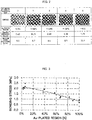
- Fig. 2 is a table showing a state of a surface of the irradiation region 12a of the first member 11, a ratio of an Au-plated region (a region in which the thin film 12 remained in the irradiation region 12a), a surface roughness Ra, and a maximum level difference Ry in each of Comparative Example (a case where no irradiation step S11 was carried out) and Examples 1 through 4.
- the maximum level difference Ry is a difference between a highest level and a lowest level in a surface profile of the irradiation region 12a.
- the ratio of the Au-plated region was obtained by (i) extracting, by carrying out image processing, a region in which the thin film 12 remained in a photograph obtained by capturing an image of the irradiation region 12a and (ii) calculating a ratio of a sum total of an area of the region thus extracted to an area of the irradiation region 12a.
- Fig. 3 is a graph showing a correlation between a bonding stress between the first member 11 and the second member 14 and a ratio of a remaining gold-plated region.
- the bonding stress is a value obtained by (i) applying a force to the bonding region 12b while gradually increasing the force and (ii) dividing the force by an area of the bonding region 12b at a time point at which the first member 11 and the second member 14 bonded to each other started separating from each other.
- a higher bonding stress means higher bonding strength.
- the bonding stress between the first member 11 and the second member 14 was not less than 0.6 MPa and not more than 1.0 MPa.
- the bonding stress between the first member 11 and the second member 14 showed a tendency to increase. That is, it was confirmed that as the ratio of the Au-plated region decreased from 100%, the bonding strength increased. Note that in the case where the irradiation step S11 was carried out eight times (Example 4), the bonding stress between the first member 11 and the second member 14 was not less than 1.8 MPa and not more than 2.5 MPa.
- the bonding stress between the first member 11 and the second member 14 is preferably not less than 1.4 MPa. This is based on the finding that, in the optical module, a substrate or a submount which corresponds to the first member 11 may be warped by 10 ⁇ m at the maximum. The inventors of the present application found that in a case where the substrate or the submount is warped by 10 ⁇ m, a bending stress of approximately 1.4 MPa at the maximum is generated in a bonding region 12b of an optical component corresponding to the second member 14.
- the bonding stress between the first member 11 and the second member 14 is not less than 1.4 MPa, it is possible to favorably maintain the bonding between the first member 11 and the second member 14 so that the first member 11 and the second member 14 do not separate from each other even in a case where the first member 11 is warped by 10 ⁇ m.
- the bonding stress between the first member 11 and the second member 14 exceeds 1.4 MPa. Accordingly, in the bonding method S1, it is preferable to repeat the irradiation step S11 until the ratio of the Au-plated region becomes not more than 60%.
- the bonding stress between the first member 11 and the second member 14 increases as the number of times the irradiation step S11 is carried out increases. This is primarily because as the number of times at which the irradiation step S11 is carried out increases, the ratio of the Au-plated region in the irradiation region 12a decreases. Further, increasing the number of times the irradiation step S11 is carried out generates secondary effects such as an increase in surface roughness Ra in the irradiation region 12a. The increase in surface roughness Ra results in an increase in area of a region in which the adhesive 13 is bonded to the base of the thin film 12. This consequently improves the bonding stress.
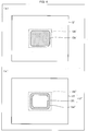
- FIG. 4 two modified examples of the bonding method S1 in accordance with Embodiment 1.
- FIG. 4 are each a top view illustrating the first member 11 after an irradiation step S11 included in a bonding method S1 in accordance with Modified Example 1 is carried out. Note that the first member 11 is completely covered with thin films 12' and 12" in (a) and (b) of Fig. 4 , respectively.
- the thin films 12' and 12" illustrated in respective (a) and (b) of Fig. 4 correspond to the thin film 12 illustrated in (c) of Fig. 1 .
- the modified example illustrated in (a) of Fig. 4 employs a configuration in which an outer circumference of an irradiation region 12a' which is irradiated with laser light in the irradiation step S11 is constituted by a smooth curved line.
- the outer circumference of the irradiation region 12a' has no angular corner (vertex) on which a bending stress is likely to concentrate. Accordingly, a bending stress which is generated when the first member 11 is warped is dispersed on the outer circumference of the irradiation region 12a'.
- the modified example illustrated in (b) of Fig. 4 employs a configuration in which an irradiation region 12a" irradiated with laser light in the irradiation step S11 is an annular region which (i) has an outer circumference and an inner circumference each of which is constituted by a smooth curved line and (ii) extends along a bonding region 12b" to which the second member 14 is bonded in the bonding step S12.
- the irradiation region 12a" partitions the thin film 12 into a thin film 121 which is located inside the irradiation region 12a" and a thin film 122 which is located outside the irradiation region 12a".
- the second member 14 is bonded to the irradiation region 12a" having the outer circumference and the inner circumference each of which is constituted by a smooth curved line, the first member 11 and the second member 14 can be bonded to each other so as to exhibit a bonding stress as high as that in the modified example illustrated in (a) of Fig. 4 .
- the configuration allows an area of the irradiation region 12a" to be smaller as compared with the modified example illustrated in (a) of Fig. 4 . This makes it possible to reduce a time required for the irradiation step S11.
- FIG. 5 another two modified examples of the bonding method S1 in accordance with Embodiment 1.
- (a) and (b) of Fig. 5 are each a top view illustrating a first member 11 after an irradiation step S11 included in a bonding method S1 in accordance with Modified Example 2 is carried out.
- the first member 11 is completely covered with thin films 22 and 22' in (a) and (b) of Fig. 5 , respectively.
- the thin films 22 and 22' illustrated in respective (a) and (b) of Fig. 5 correspond to the thin film 12 illustrated in (c) of Fig. 1 .
- the modified example illustrated in (a) of Fig. 5 employs a configuration in which an irradiation region 22a irradiated with laser light in the irradiation step S11 contains a bonding region 22b to which a second member 14 is bonded in a bonding step S12.
- the irradiation region 22a contains an outer circumference of the bonding region 22b on which outer circumference a bending stress generated when the first member 11 is warped is likely to concentrate. Accordingly, as compared with a case where the irradiation region 12a does not contain the bonding region 12b (see Fig. 1 ), a structure bonded by the bonding method in accordance with Modified Example 2 exhibits a higher bonding stress.
- Modified Example 2 it is preferable in Modified Example 2 to apply an adhesive 13 to a region containing the irradiation region 22a. That is, it is preferable that the irradiation region 22a be a part of a region to which the adhesive 13 is applied and the bonding region 22b be a part of the irradiation region 22a. This makes it possible to cover, with the adhesive 13, the region in which the base of the thin film 22 is exposed in the irradiation region 22a. Accordingly, it is possible to prevent a deterioration such as corrosion in the region.
- the modified example illustrated in (b) of Fig. 5 employs a configuration in which an irradiation region 22a' irradiated with laser light in the irradiation step S11 is an annular region which (i) contains an outer circumference of a bonding region 22b' to which the second member 14 is bonded in the bonding step S12 and (ii) extends along the outer circumference of the bonding region 22b'.
- the irradiation region 22a' partitions the thin film 22' into a thin film 221 which is located inside the irradiation region 22a' and a thin film 222 which is located outside the irradiation region 22a'.
- the irradiation region 22a' contains the outer circumference of the bonding region 22b', the first member 11 and the second member 14 can be bonded to each other so as to exhibit a bonding stress as high as that in the modified example illustrated in (a) of Fig. 5 . Further, the configuration allows an area of the irradiation region 22a' to be smaller as compared with the modified example illustrated in (a) of Fig. 5 . This makes it possible to reduce a time required for the irradiation step S11.
- (b) of Fig. 5 illustrates the irradiation region 22a' having the outer circumference and the inner circumference each of which is constituted by a smooth curved line. Note, however, that the outer circumference and the inner circumference of the irradiation region 22a' can each have an angular corner (vertex). For example, the outer circumference and the inner circumference of the irradiation region 22a' can each have a rectangular shape.
- a bonding method in accordance with Embodiment 1 is a bonding method for bonding a first member and a second member to each other, the first member being made of a material other than gold and having a surface on which a gold thin film is formed, the second member being made of a material other than gold, the bonding method including the steps of: (1) irradiating, with laser light, at least part of a specific region of the surface of the first member, so that a base of the thin film is exposed in the at least part of the specific region; and (2) bonding the second member to the specific region by use of an adhesive.
- the second member is bonded to the base which is made of the material other than gold, instead of being bonded to the gold thin film. This makes it possible to achieve a higher adhesive force without carrying out any special treatment on the second member, as compared with a case where the second member is bonded to the gold thin film.
- the bonding method in accordance with Embodiment 1 is preferably configured such that the step (1) is a step of sporadically irradiating each point in the specific region with laser light.
- regions in each of which the base is exposed can be densely scattered in the irradiation region. Further, in a case where the step (1) is repeatedly carried out, it is possible to (i) gradually increase, in the specific region, a ratio of the regions in each of which the base is exposed and (ii) gradually reduce, in the specific region, a ratio of a region in which the thin film remains.
- the bonding method in accordance with Embodiment 1 is preferably configured such that the step (1) is repeated until a sum total of an area of a region in which the thin film remains in the specific region becomes not more than 60% of an area of the specific region.
- a bonding stress between the first member and the second member exceeds a predetermined value (1.4 MPa) which is considered to be sufficient for practical use.
- the bonding method in accordance with Embodiment 1 is preferably configured such that the specific region is contained in a region to which the second member is bonded on the surface of the first member.
- the configuration makes it possible to prevent the base of the thin film from coming into contact with outside air after the step (2) is carried out. Accordingly, it is possible to prevent a deterioration such as corrosion of the base of the thin film.
- the bonding method in accordance with Embodiment 1 is preferably configured such that the specific region is a region whose outer circumference is constituted by a smooth curved line.
- the outer circumference of the specific region has no angular corner on which a bending stress is likely to concentrate. Accordingly, a bending stress which is generated when the first member is warped is dispersed on the outer circumference of the specific region. This makes it possible to more strongly bond the first member and the second member to each other, as compared with a case where the outer circumference of the specific region has an angular corner.
- the bonding method in accordance with Embodiment 1 is preferably configured such that the specific region is an annular region which extends along an outer circumference of a region to which the second member is bonded on the surface of the first member.
- the configuration allows an area of the irradiation region to be smaller. This makes it possible to reduce a time required for the step (1).
- the bonding method in accordance with Embodiment 1 is preferably configured such that the second member is a transparent member.
- the configuration makes it possible to irradiate the adhesive with light (e.g., ultraviolet) through the second member, so that the step (2) can be easily carried out.
- light e.g., ultraviolet
- a manufacturing method in accordance with Embodiment 1 is a manufacturing method for manufacturing a structure including a first member and a second member, the first member being made of a material other than gold and having a surface on which a gold thin film is formed, the manufacturing method including the steps of: (1) irradiating, with laser light, a specific region of the surface of the first member, so that a base of the thin film is exposed in the specific region; and (2) bonding the second member to the specific region by use of an adhesive.
- the manufacturing method in accordance with Embodiment 1 brings about an effect similar to that of the bonding method in accordance with Embodiment 1.
- a structure in accordance with Embodiment 1 is a structure including: a first member; and a second member, the first member being made of a material other than gold and having a surface on which a gold thin film is formed, the surface of the first member containing a specific region in which a base of the thin film is exposed by irradiation with laser light, the second member being bonded to the specific region by use of an adhesive.
- the structure in accordance with Embodiment 1 brings about an effect similar to that of the bonding method in accordance with Embodiment 1.
- the present invention is applicable to a bonding method for bonding two members to each other by use of an adhesive. Further, the present invention is applicable to a structure including two members which are bonded to each other and a manufacturing method for manufacturing the structure.
Landscapes
- Chemical & Material Sciences (AREA)
- Organic Chemistry (AREA)
- Engineering & Computer Science (AREA)
- General Chemical & Material Sciences (AREA)
- Life Sciences & Earth Sciences (AREA)
- Chemical Kinetics & Catalysis (AREA)
- Ceramic Engineering (AREA)
- Geochemistry & Mineralogy (AREA)
- Materials Engineering (AREA)
- Physics & Mathematics (AREA)
- Plasma & Fusion (AREA)
- Thermal Sciences (AREA)
- Adhesives Or Adhesive Processes (AREA)
- Laser Beam Processing (AREA)
- Laminated Bodies (AREA)
Abstract
Description
- The present invention relates to a method for bonding two members to each other by use of an adhesive. The present invention also relates to a structure including two members which are bonded to each other and a method for manufacturing the structure.
- As a method for bonding two members to each other, a bonding method using solder and a bonding method using an adhesive have widely been used. For example, solder is used for bonding an electronic component to a submount of a laser module and an adhesive is used for bonding an optical component to the submount of the laser module.
- In a case where the electronic component and the optical component are bonded to the submount, the following problem occurs. That is, in a case where the electronic component is bonded to the submount by use of solder, it is necessary to plate a surface of the submount with gold in order to obtain sufficient bonding strength. However, a gold-plated surface of the submount makes it difficult to bond the optical component to the submount by use of an adhesive.
- The following describes why it is difficult to bond a member to another member having a surface plated with gold. That is, bonding by an adhesive is typically strengthened by intermolecular force generated between molecules constituting the adhesive and atoms or molecules constituting a surface to be bonded of a member. However, since gold atoms are nonpolar atoms, in a case where the surface to be bonded is made of gold, it is impossible to strengthen the bonding by the adhesive by using the intermolecular force.
-
Patent Literature 1 discloses a bonding method as a technique usable for avoiding the problem. According to the bonding method disclosed inPatent Literature 1, an FIPG (Formed In Place Gasket) which has high bonding strength with respect to metal is used for bonding a metal member and a synthetic resin member to each other. - Japanese Patent Application Publication, Tokukai, No.
2013-199834 (Publication date: October 3, 2013 - However, a technique of bonding a second member (e.g., optical component) to a first member (e.g., submount) having a gold-plated surface requires, in addition to use of the FIPG as an adhesive, a step of providing, on a surface of the second member, a synthetic resin material containing aluminum powder. Further, use of the technique also requires a step of causing a synthetic resin material to contain aluminum powder and a step of appropriately controlling the synthetic resin material.
- For this reason, there is a demand for realization of a bonding method which is a method for bonding a gold-plated first member and a second member to each other and is capable of achieving a high adhesive force without carrying out any special treatment on the second member.
- The present invention has been accomplished in view of the problem, and an object of the present invention is to provide a bonding method which is a method for bonding a first member and a second member to each other and is capable of achieving a high adhesive force without carrying out any special treatment on the second member, even in a case where the first member has a surface on which a gold thin film is formed. Another object of the present invention is to provide a manufacturing method and a structure each of which brings about an effect similar to that of the bonding method.
- In order to attain the object, a bonding method in accordance with the present invention is a bonding method for bonding a first member and a second member to each other, the first member being made of a material other than gold and having a surface on which a gold thin film is formed, the second member being made of a material other than gold, the bonding method including the steps of: (1) irradiating, with laser light, at least part of a specific region of the surface of the first member, so that a base of the thin film is exposed in the at least part of the specific region; and (2) bonding the second member to the specific region by use of an adhesive.
- In order to attain the object, a manufacturing method for manufacturing a structure including a first member and a second member, the first member being made of a material other than gold and having a surface on which a gold thin film is formed, the manufacturing method including the steps of: (1) irradiating, with laser light, a specific region of the surface of the first member, so that a base of the thin film is exposed in the specific region; and (2) bonding the second member to the specific region by use of an adhesive.
- In order to attain the object, a structure in accordance with the present invention is a structure including: a first member; and a second member, the first member being made of a material other than gold and having a surface on which a gold thin film is formed, the surface of the first member containing a specific region in which a base of the thin film is exposed by irradiation with laser light, the second member being bonded to the specific region by use of an adhesive.
- With the present invention, it is possible to achieve a high adhesive force without carrying out any special treatment on the second member, even in a case where the first member has a surface on which a gold thin film is formed.
-
- (a) of
Fig. 1 is a flow chart showing a flow of a bonding method in accordance with an embodiment of the present invention. (b) ofFig. 1 is a perspective view illustrating a first member before an irradiation step is carried out. (c) ofFig. 1 is a perspective view illustrating the first member after the irradiation step is carried out. (d) ofFig. 1 is a perspective view illustrating the first member and a second member after a bonding step is carried out. -
Fig. 2 is a table showing a state of a surface of an irradiation region of a first member, a ratio of an Au-plated region, a surface roughness, and a maximum level difference in each of Comparative Example and Examples 1 through 4. -
Fig. 3 is a graph showing a correlation between a bonding stress between the first member and the second member and the ratio of the Au-plated region. - (a) and (b) of
Fig. 4 are each a top view illustrating a first member and a thin film after an irradiation step included in a bonding method in accordance with a modified example of the present invention is carried out. - (a) and (b) of
Fig. 5 are each a top view illustrating a first member and a thin film after an irradiation step included in a bonding method in accordance with another modified example of the present invention is carried out. - The following description will discuss, with reference to
Fig. 1 , a bonding method in accordance with an embodiment of the present invention. - (a) of
Fig. 1 is a flow chart showing a bonding method S1 in accordance withEmbodiment 1.
The bonding method S1 is a method for bonding afirst member 11 and asecond member 14 to each other and includes an irradiation step S11 and a bonding step S12 as illustrated in (a) ofFig. 1 . The following description will discuss, with reference to also (b) through (d) ofFig. 1 , the steps included in the bonding method S1. - (b) of
Fig. 1 is a perspective view illustrating thefirst member 11 before the irradiation step S11 is carried out. Thefirst member 11 is made of a material other than gold and has a surface on which a goldthin film 12 is formed (specifically, thefirst member 11 has a surface which is plated with gold), as illustrated in (b) ofFig. 1 . -
Embodiment 1 employs, as thefirst member 11, a member in which, on a surface of acopper base material 11a, a nickelthin film 11b and a palladiumthin film 11c are formed in this order (specifically, the surface of thecopper base material 11a is plated with nickel and palladium). In this case, the goldthin film 12 is formed on the palladiumthin film 11c. Note that materials of thebase material 11a and thethin films thin films - The irradiation step S11 is a step of irradiating, with laser light, at least part of a specific region (hereinafter referred to as "irradiation region") 12a on the
thin film 12. In a case where the irradiation step S11 is carried out, gold constituting thethin film 12 is evaporated in the at least part of theirradiation region 12a, so that a base of thethin film 12 is exposed. (c) ofFig. 1 is a perspective view illustrating thefirst member 11 after the irradiation step S11 is carried out. - In
Embodiment 1, each point in theirradiation region 12a is sporadically irradiated with laser light in the irradiation step S11. Specifically, by using a laser marking technique, each irradiation point in theirradiation region 12a is irradiated with pulsed laser light, one pulse at a time. Accordingly, regions in each of which the base is exposed can be densely scattered in theirradiation region 12a. In a case where the irradiation step S11 is repeatedly carried out, it is possible to (i) gradually increase, in theirradiation region 12a, a ratio of the regions in each of which the base is exposed and (ii) gradually reduce, in theirradiation region 12a, a ratio of a region in which thethin film 12 remains. - The bonding step S12 is a step of bonding the
second member 14 to a specific region (hereinafter referred to as "bonding region") 12b on thethin film 12 by use of an adhesive 13. By carrying out the bonding step S12, bonding of thefirst member 11 and thesecond member 14 to each other is completed. (d) ofFig. 1 is a perspective view illustrating astructure 1 including thefirst member 11 and thesecond member 14 which have been bonded to each other by the bonding method S1 in accordance withEmbodiment 1. - In
Embodiment 1, a photocurable resin such as an ultraviolet curable resin is employed as a material of the adhesive 13 and a transparent material such as glass is employed as a material of thesecond member 14. This makes it possible to irradiate theadhesive 13 with light (e.g., ultraviolet) through thesecond member 14, so that the bonding step S12 can be easily carried out. Note, however, that the material of thesecond member 14 can be selected from any materials other than gold. Further, theadhesive 13 is not limited to the photocurable resin which is cured by light, but can be a resin which is cured by heat or a chemical reaction. - In
Embodiment 1, as illustrated in (b) ofFig. 1 , thebonding region 12b is set to encompass theirradiation region 12a. In other words, theirradiation region 12a is set to be encompassed in thebonding region 12b. As illustrated in (c) ofFig. 1 , this makes it possible to prevent the base (inEmbodiment 1, thebase material 11a, thethin film 11b, or thethin film 11c) of thethin film 12 from coming into contact with outside air after the bonding step S12 is carried out. Accordingly, it is possible to prevent a deterioration such as corrosion of the base of thethin film 12. - As described above, according to the bonding method S1 in accordance with
Embodiment 1, (1) the base of thethin film 12 is exposed in the at least part of theirradiation region 12a by irradiation with laser light, and then (2) thesecond member 14 is bonded to theirradiation region 12a by use of the adhesive 13. Accordingly, in the at least part of theirradiation region 12a, thesecond member 14 is bonded to the base (thecopper base material 11a, the nickelthin film 11b, or the palladiumthin film 11c) made of the material other than gold, instead of being bonded to the goldthin film 12. This can achieve a higher adhesive force as compared with a case where thesecond member 14 is bonded to the goldthin film 12. - Note that the bonding method S1 in accordance with
Embodiment 1 is also applicable to a method for manufacturing thestructure 1. An optical module can be an example of thestructure 1 which can be manufactured by the bonding method S1 in accordance withEmbodiment 1. In the optical module, (1) a laser light source (e.g., a laser diode (LD)) which emits laser light, (2) an electronic component for driving the LD, (3) an optical member (e.g., a mirror or a lens) which directs the laser light to an optical fiber, and the like are provided on a substrate or a submount stacked on the substrate. Note that a surface of the substrate or the submount is often plated with gold. Thus, the bonding method in accordance with the present invention is applied when the substrate or the submount (corresponding to the first member 11) and the optical member (corresponding to the second member 14) are bonded to each other. This makes it possible to favorably bond the optical member to the surface of the substrate or the submount by use of an adhesive, even in a case where the surface of the substrate or the submount is plated with gold. The structure 1 (e.g., the optical module) which is manufactured by the bonding method S1 in accordance withEmbodiment 1 is also encompassed in the scope of the present invention. - The following description will discuss examples of the bonding method S1 with reference to
Figs. 2 and 3 . The following description will discuss (1) Example 1 in which the irradiation step S11 is carried out once, (2) Example in which the irradiation step S11 is carried out twice, (3) Example 3 in which the irradiation step S11 is carried out four times, and (4) Example 4 in which the irradiation step S11 is carried out eight times. - Note that Examples 1 through 4 employed, as the
first member 11, a member in which on a surface of acopper base material 11a, a nickelthin film 11b having a thickness of 1 µm and a palladiumthin film 11c having a thickness of 0.1 µm had been formed in this order by a plating method. Further, a gold-plated film which had been formed by the plating method so as to have a thickness of 0.1 µm was employed as thethin film 12. A mirror made of glass was employed as thesecond member 14. Thethin film 12 had abonding region 12b to which thesecond member 14 was bonded and which had a rectangular shape identical to a shape of a bottom surface of the mirror. In Examples 1 through 4, a mirror having a bottom surface with an area of 27 mm2 was employed as the mirror serving as thesecond member 14. - In the irradiation step S11, each of irradiation points which were distributed at a predetermined density in an
irradiation region 12a was irradiated with pulsed laser light having a wavelength of 1064 nm, one pulse at a time. In Examples 1, 2, 3, and 4, the irradiation step S11 was carried out once, twice, four times, and eight times, respectively. - In the bonding step S12, (1) an adhesive 13 (ultraviolet curable resin) was applied to the
bonding region 12b, (2) thesecond member 14 was placed on thebonding region 12b via the adhesive 13, and (3) the adhesive 13 was irradiated with ultraviolet through thesecond member 14. -
Fig. 2 is a table showing a state of a surface of theirradiation region 12a of thefirst member 11, a ratio of an Au-plated region (a region in which thethin film 12 remained in theirradiation region 12a), a surface roughness Ra, and a maximum level difference Ry in each of Comparative Example (a case where no irradiation step S11 was carried out) and Examples 1 through 4. Note that the maximum level difference Ry is a difference between a highest level and a lowest level in a surface profile of theirradiation region 12a. - As shown in
Fig. 2 , it was confirmed that as the number of times the irradiation step S11 was carried out increased, the ratio of the Au-plated region gradually decreased, i.e., a ratio of a region in which a base of thethin film 12 was exposed gradually increased. Further, it was confirmed that as the number of times the irradiation step S11 was carried out increased, the surface roughness Ra and the maximum level difference Ry showed a tendency to increase. - Note that the ratio of the Au-plated region was obtained by (i) extracting, by carrying out image processing, a region in which the
thin film 12 remained in a photograph obtained by capturing an image of theirradiation region 12a and (ii) calculating a ratio of a sum total of an area of the region thus extracted to an area of theirradiation region 12a. -
Fig. 3 is a graph showing a correlation between a bonding stress between thefirst member 11 and thesecond member 14 and a ratio of a remaining gold-plated region. Note that the bonding stress is a value obtained by (i) applying a force to thebonding region 12b while gradually increasing the force and (ii) dividing the force by an area of thebonding region 12b at a time point at which thefirst member 11 and thesecond member 14 bonded to each other started separating from each other. A higher bonding stress means higher bonding strength. - As shown in
Fig. 3 , in a case where the ratio of the Au-plated region was 100% (Comparative Example), the bonding stress between thefirst member 11 and thesecond member 14 was not less than 0.6 MPa and not more than 1.0 MPa. As the ratio of the Au-plated region decreased from 100%, the bonding stress between thefirst member 11 and thesecond member 14 showed a tendency to increase. That is, it was confirmed that as the ratio of the Au-plated region decreased from 100%, the bonding strength increased. Note that in the case where the irradiation step S11 was carried out eight times (Example 4), the bonding stress between thefirst member 11 and thesecond member 14 was not less than 1.8 MPa and not more than 2.5 MPa. - In a case where an optical module is manufactured by the bonding method S1, the bonding stress between the
first member 11 and thesecond member 14 is preferably not less than 1.4 MPa. This is based on the finding that, in the optical module, a substrate or a submount which corresponds to thefirst member 11 may be warped by 10 µm at the maximum. The inventors of the present application found that in a case where the substrate or the submount is warped by 10 µm, a bending stress of approximately 1.4 MPa at the maximum is generated in abonding region 12b of an optical component corresponding to thesecond member 14. In a case where the bonding stress between thefirst member 11 and thesecond member 14 is not less than 1.4 MPa, it is possible to favorably maintain the bonding between thefirst member 11 and thesecond member 14 so that thefirst member 11 and thesecond member 14 do not separate from each other even in a case where thefirst member 11 is warped by 10 µm. - According to the results of measurement of bonding stress shown in
Fig. 3 , in a case where the ratio of the Au-plated region is not more than 60% (Examples 2 through 4), the bonding stress between thefirst member 11 and thesecond member 14 exceeds 1.4 MPa. Accordingly, in the bonding method S1, it is preferable to repeat the irradiation step S11 until the ratio of the Au-plated region becomes not more than 60%. - As described above, in the bonding method S1, the bonding stress between the
first member 11 and thesecond member 14 increases as the number of times the irradiation step S11 is carried out increases. This is primarily because as the number of times at which the irradiation step S11 is carried out increases, the ratio of the Au-plated region in theirradiation region 12a decreases. Further, increasing the number of times the irradiation step S11 is carried out generates secondary effects such as an increase in surface roughness Ra in theirradiation region 12a. The increase in surface roughness Ra results in an increase in area of a region in which the adhesive 13 is bonded to the base of thethin film 12. This consequently improves the bonding stress. - The following description will discuss, with reference to (a) and (b) of
Fig. 4 , two modified examples of the bonding method S1 in accordance withEmbodiment 1. (a) and (b) ofFig. 4 are each a top view illustrating thefirst member 11 after an irradiation step S11 included in a bonding method S1 in accordance with Modified Example 1 is carried out. Note that thefirst member 11 is completely covered withthin films 12' and 12" in (a) and (b) ofFig. 4 , respectively. Thethin films 12' and 12" illustrated in respective (a) and (b) ofFig. 4 correspond to thethin film 12 illustrated in (c) ofFig. 1 . - The modified example illustrated in (a) of
Fig. 4 employs a configuration in which an outer circumference of anirradiation region 12a' which is irradiated with laser light in the irradiation step S11 is constituted by a smooth curved line. With the configuration, the outer circumference of theirradiation region 12a' has no angular corner (vertex) on which a bending stress is likely to concentrate. Accordingly, a bending stress which is generated when thefirst member 11 is warped is dispersed on the outer circumference of theirradiation region 12a'. This allows a structure bonded by the bonding method in accordance with Modified Example 1 to exhibit a higher bonding stress, as compared with a case where theirradiation region 12a has a rectangular shape (seeFig. 1 ). - The modified example illustrated in (b) of
Fig. 4 employs a configuration in which anirradiation region 12a" irradiated with laser light in the irradiation step S11 is an annular region which (i) has an outer circumference and an inner circumference each of which is constituted by a smooth curved line and (ii) extends along abonding region 12b" to which thesecond member 14 is bonded in the bonding step S12. Theirradiation region 12a" partitions thethin film 12 into athin film 121 which is located inside theirradiation region 12a" and athin film 122 which is located outside theirradiation region 12a". - With the configuration, since the
second member 14 is bonded to theirradiation region 12a" having the outer circumference and the inner circumference each of which is constituted by a smooth curved line, thefirst member 11 and thesecond member 14 can be bonded to each other so as to exhibit a bonding stress as high as that in the modified example illustrated in (a) ofFig. 4 . Further, the configuration allows an area of theirradiation region 12a" to be smaller as compared with the modified example illustrated in (a) ofFig. 4 . This makes it possible to reduce a time required for the irradiation step S11. - The following description will discuss, with reference to
Fig. 5 , another two modified examples of the bonding method S1 in accordance withEmbodiment 1. (a) and (b) ofFig. 5 are each a top view illustrating afirst member 11 after an irradiation step S11 included in a bonding method S1 in accordance with Modified Example 2 is carried out. Note that thefirst member 11 is completely covered withthin films 22 and 22' in (a) and (b) ofFig. 5 , respectively. Thethin films 22 and 22' illustrated in respective (a) and (b) ofFig. 5 correspond to thethin film 12 illustrated in (c) ofFig. 1 . - The modified example illustrated in (a) of
Fig. 5 employs a configuration in which anirradiation region 22a irradiated with laser light in the irradiation step S11 contains abonding region 22b to which asecond member 14 is bonded in a bonding step S12. With the configuration, theirradiation region 22a contains an outer circumference of thebonding region 22b on which outer circumference a bending stress generated when thefirst member 11 is warped is likely to concentrate. Accordingly, as compared with a case where theirradiation region 12a does not contain thebonding region 12b (seeFig. 1 ), a structure bonded by the bonding method in accordance with Modified Example 2 exhibits a higher bonding stress. - Note, however, that in a case where a region of the
irradiation region 22a in which region a base of thethin film 22 is exposed comes into contact with outside air, a deterioration such as corrosion may occur in the region in which the base of thethin film 22 is exposed. In order to prevent such a deterioration, it is preferable in Modified Example 2 to apply an adhesive 13 to a region containing theirradiation region 22a. That is, it is preferable that theirradiation region 22a be a part of a region to which the adhesive 13 is applied and thebonding region 22b be a part of theirradiation region 22a. This makes it possible to cover, with the adhesive 13, the region in which the base of thethin film 22 is exposed in theirradiation region 22a. Accordingly, it is possible to prevent a deterioration such as corrosion in the region. - The modified example illustrated in (b) of
Fig. 5 employs a configuration in which anirradiation region 22a' irradiated with laser light in the irradiation step S11 is an annular region which (i) contains an outer circumference of abonding region 22b' to which thesecond member 14 is bonded in the bonding step S12 and (ii) extends along the outer circumference of thebonding region 22b'. Theirradiation region 22a' partitions the thin film 22' into athin film 221 which is located inside theirradiation region 22a' and athin film 222 which is located outside theirradiation region 22a'. - With the configuration, since the
irradiation region 22a' contains the outer circumference of thebonding region 22b', thefirst member 11 and thesecond member 14 can be bonded to each other so as to exhibit a bonding stress as high as that in the modified example illustrated in (a) ofFig. 5 . Further, the configuration allows an area of theirradiation region 22a' to be smaller as compared with the modified example illustrated in (a) ofFig. 5 . This makes it possible to reduce a time required for the irradiation step S11. - In Modified Example 2, (b) of
Fig. 5 illustrates theirradiation region 22a' having the outer circumference and the inner circumference each of which is constituted by a smooth curved line. Note, however, that the outer circumference and the inner circumference of theirradiation region 22a' can each have an angular corner (vertex). For example, the outer circumference and the inner circumference of theirradiation region 22a' can each have a rectangular shape. - A bonding method in accordance with
Embodiment 1 is a bonding method for bonding a first member and a second member to each other, the first member being made of a material other than gold and having a surface on which a gold thin film is formed, the second member being made of a material other than gold, the bonding method including the steps of: (1) irradiating, with laser light, at least part of a specific region of the surface of the first member, so that a base of the thin film is exposed in the at least part of the specific region; and (2) bonding the second member to the specific region by use of an adhesive. - With the configuration, the second member is bonded to the base which is made of the material other than gold, instead of being bonded to the gold thin film. This makes it possible to achieve a higher adhesive force without carrying out any special treatment on the second member, as compared with a case where the second member is bonded to the gold thin film.
- The bonding method in accordance with
Embodiment 1 is preferably configured such that the step (1) is a step of sporadically irradiating each point in the specific region with laser light. - With the configuration, regions in each of which the base is exposed can be densely scattered in the irradiation region. Further, in a case where the step (1) is repeatedly carried out, it is possible to (i) gradually increase, in the specific region, a ratio of the regions in each of which the base is exposed and (ii) gradually reduce, in the specific region, a ratio of a region in which the thin film remains.
- The bonding method in accordance with
Embodiment 1 is preferably configured such that the step (1) is repeated until a sum total of an area of a region in which the thin film remains in the specific region becomes not more than 60% of an area of the specific region. - With the configuration, a bonding stress between the first member and the second member exceeds a predetermined value (1.4 MPa) which is considered to be sufficient for practical use.
- The bonding method in accordance with
Embodiment 1 is preferably configured such that the specific region is contained in a region to which the second member is bonded on the surface of the first member. - The configuration makes it possible to prevent the base of the thin film from coming into contact with outside air after the step (2) is carried out. Accordingly, it is possible to prevent a deterioration such as corrosion of the base of the thin film.
- The bonding method in accordance with
Embodiment 1 is preferably configured such that the specific region is a region whose outer circumference is constituted by a smooth curved line. - With the configuration, the outer circumference of the specific region has no angular corner on which a bending stress is likely to concentrate. Accordingly, a bending stress which is generated when the first member is warped is dispersed on the outer circumference of the specific region. This makes it possible to more strongly bond the first member and the second member to each other, as compared with a case where the outer circumference of the specific region has an angular corner.
- The bonding method in accordance with
Embodiment 1 is preferably configured such that the specific region is an annular region which extends along an outer circumference of a region to which the second member is bonded on the surface of the first member. - The configuration allows an area of the irradiation region to be smaller. This makes it possible to reduce a time required for the step (1).
- The bonding method in accordance with
Embodiment 1 is preferably configured such that the second member is a transparent member. - The configuration makes it possible to irradiate the adhesive with light (e.g., ultraviolet) through the second member, so that the step (2) can be easily carried out.
- A manufacturing method in accordance with
Embodiment 1 is a manufacturing method for manufacturing a structure including a first member and a second member, the first member being made of a material other than gold and having a surface on which a gold thin film is formed, the manufacturing method including the steps of: (1) irradiating, with laser light, a specific region of the surface of the first member, so that a base of the thin film is exposed in the specific region; and (2) bonding the second member to the specific region by use of an adhesive. - The manufacturing method in accordance with
Embodiment 1 brings about an effect similar to that of the bonding method in accordance withEmbodiment 1. - A structure in accordance with
Embodiment 1 is a structure including: a first member; and a second member, the first member being made of a material other than gold and having a surface on which a gold thin film is formed, the surface of the first member containing a specific region in which a base of the thin film is exposed by irradiation with laser light, the second member being bonded to the specific region by use of an adhesive. - The structure in accordance with
Embodiment 1 brings about an effect similar to that of the bonding method in accordance withEmbodiment 1. - The present invention is not limited to the embodiments, but can be altered by a skilled person in the art within the scope of the claims. An embodiment derived from a proper combination of technical means each disclosed in a different embodiment is also encompassed in the technical scope of the present invention.
- The present invention is applicable to a bonding method for bonding two members to each other by use of an adhesive. Further, the present invention is applicable to a structure including two members which are bonded to each other and a manufacturing method for manufacturing the structure.
-
- S1: Bonding method
- S11: Irradiation step
- S12: Bonding step
- 1: Structure
- 11: First member
- 11a: Base material
- 11b: Thin film
- 11c: Thin film
- 12: Thin film
- 12a: Irradiation region (specific region)
- 12b: Bonding region (region to which second member is bonded)
- 13: Adhesive
- 14: Second member
Claims (9)
- A bonding method for bonding a first member and a second member to each other, the first member being made of a material other than gold and having a surface on which a gold thin film is formed, the second member being made of a material other than gold,
said bonding method comprising the steps of:(1) irradiating, with laser light, at least part of a specific region of the surface of the first member, so that a base of the thin film is exposed in the at least part of the specific region; and(2) bonding the second member to the specific region by use of an adhesive. - The bonding method as set forth in claim 1, wherein the step (1) is a step of sporadically irradiating each point in the specific region with laser light.
- The bonding method as set forth in claim 2, wherein the step (1) is repeated until a sum total of an area of a region in which the thin film remains in the specific region becomes not more than 60% of an area of the specific region.
- The bonding method as set forth in any one of claims 1 through 3, wherein the specific region is contained in a region to which the second member is bonded on the surface of the first member.
- The bonding method as set forth in any one of claims 1 through 4, wherein the specific region is a region whose outer circumference is constituted by a smooth curved line.
- The bonding method as set forth in any one of claims 1 through 5, wherein the specific region is an annular region which extends along an outer circumference of a region to which the second member is bonded on the surface of the first member.
- The bonding method as set forth in any one of claims 1 through 6, wherein the second member is a transparent member.
- A manufacturing method for manufacturing a structure including a first member and a second member, the first member being made of a material other than gold and having a surface on which a gold thin film is formed,
said manufacturing method comprising the steps of:(1) irradiating, with laser light, a specific region of the surface of the first member, so that a base of the thin film is exposed in the specific region; and(2) bonding the second member to the specific region by use of an adhesive. - A structure comprising:a first member; anda second member,the first member being made of a material other than gold and having a surface on which a gold thin film is formed,the second member being made of a material other than gold,the surface of the first member containing a specific region in at least part of which a base of the thin film is exposed by irradiation with laser light,the second member being bonded to the specific region by use of an adhesive.
Applications Claiming Priority (2)
| Application Number | Priority Date | Filing Date | Title |
|---|---|---|---|
| JP2014136226A JP5917613B2 (en) | 2014-07-01 | 2014-07-01 | Adhesion method and structure manufacturing method |
| PCT/JP2015/056140 WO2016002255A1 (en) | 2014-07-01 | 2015-03-03 | Bonding method, method for manufacturing structure, and structure |
Publications (3)
| Publication Number | Publication Date |
|---|---|
| EP3165583A1 true EP3165583A1 (en) | 2017-05-10 |
| EP3165583A4 EP3165583A4 (en) | 2017-07-05 |
| EP3165583B1 EP3165583B1 (en) | 2024-09-04 |
Family
ID=55018818
Family Applications (1)
| Application Number | Title | Priority Date | Filing Date |
|---|---|---|---|
| EP15814156.4A Active EP3165583B1 (en) | 2014-07-01 | 2015-03-03 | Bonding method, method for manufacturing structure, and structure |
Country Status (5)
| Country | Link |
|---|---|
| US (1) | US10668696B2 (en) |
| EP (1) | EP3165583B1 (en) |
| JP (1) | JP5917613B2 (en) |
| CN (1) | CN106661385A (en) |
| WO (1) | WO2016002255A1 (en) |
Families Citing this family (1)
| Publication number | Priority date | Publication date | Assignee | Title |
|---|---|---|---|---|
| JP7145054B2 (en) * | 2018-11-26 | 2022-09-30 | 京セラ株式会社 | Semiconductor device package and semiconductor device |
Family Cites Families (16)
| Publication number | Priority date | Publication date | Assignee | Title |
|---|---|---|---|---|
| JPH065699B2 (en) * | 1987-09-16 | 1994-01-19 | 日本電気株式会社 | Semiconductor device |
| WO1998003600A1 (en) | 1996-07-23 | 1998-01-29 | Ciba Specialty Chemicals Holding Inc. | Metal surface treatment |
| JP2000138311A (en) | 1998-10-29 | 2000-05-16 | Toyo Commun Equip Co Ltd | Package structure of piezoelectric device |
| JP3317926B2 (en) * | 1999-06-14 | 2002-08-26 | 埼玉日本電気株式会社 | Surface acoustic wave device |
| JP2001242363A (en) * | 2000-03-01 | 2001-09-07 | Ngk Insulators Ltd | Adhesive structure of optical parts |
| JP3427038B2 (en) * | 2000-03-31 | 2003-07-14 | 京セラ株式会社 | Method of manufacturing piezoelectric device |
| JP2002084159A (en) * | 2000-09-06 | 2002-03-22 | Daishinku Corp | Surface mount type piezoelectric vibrator |
| JP4349001B2 (en) | 2003-05-28 | 2009-10-21 | 住友電気工業株式会社 | Optical transmission module |
| JP4646690B2 (en) * | 2005-05-10 | 2011-03-09 | ミヤチテクノス株式会社 | Gold plating peeling device |
| JP2007167936A (en) * | 2005-12-26 | 2007-07-05 | Miyachi Technos Corp | Gold plating peeling method and gold plating peeling apparatus |
| JP2008205265A (en) | 2007-02-21 | 2008-09-04 | Kyocera Corp | Electronic component mounting board |
| JP5320863B2 (en) * | 2008-07-02 | 2013-10-23 | オムロン株式会社 | Electronic components |
| JP5240912B2 (en) * | 2008-08-29 | 2013-07-17 | 京セラクリスタルデバイス株式会社 | Piezoelectric device manufacturing method and piezoelectric vibration element mounting apparatus |
| JP2013199834A (en) | 2012-03-23 | 2013-10-03 | Fts:Kk | Joint structure for metal member and synthetic resin member |
| JP6155551B2 (en) | 2012-04-10 | 2017-07-05 | セイコーエプソン株式会社 | Electronic device, electronic apparatus, and method for manufacturing electronic device |
| JP2014012284A (en) * | 2012-07-04 | 2014-01-23 | Toyota Motor Corp | Heating method, and joining method |
-
2014
- 2014-07-01 JP JP2014136226A patent/JP5917613B2/en active Active
-
2015
- 2015-03-03 EP EP15814156.4A patent/EP3165583B1/en active Active
- 2015-03-03 WO PCT/JP2015/056140 patent/WO2016002255A1/en not_active Ceased
- 2015-03-03 CN CN201580033301.7A patent/CN106661385A/en active Pending
-
2016
- 2016-12-22 US US15/388,070 patent/US10668696B2/en active Active
Also Published As
| Publication number | Publication date |
|---|---|
| CN106661385A (en) | 2017-05-10 |
| JP5917613B2 (en) | 2016-05-18 |
| US10668696B2 (en) | 2020-06-02 |
| US20170100917A1 (en) | 2017-04-13 |
| WO2016002255A1 (en) | 2016-01-07 |
| EP3165583A4 (en) | 2017-07-05 |
| EP3165583B1 (en) | 2024-09-04 |
| JP2016014099A (en) | 2016-01-28 |
Similar Documents
| Publication | Publication Date | Title |
|---|---|---|
| CN104718468B (en) | Manufacturing method of light control panel | |
| JP2022133477A (en) | Laser Diode Modules, Devices and Methods of Fabricating Chips on Submount Modules | |
| CN104662460B (en) | Optical module | |
| TW201023640A (en) | Image sensor camera module and method of manufacturing the same | |
| US8911581B2 (en) | Composite light guide plate manufacturing method | |
| CN104160791B (en) | metal foil with carrier | |
| US10230158B2 (en) | Method for making housing | |
| US10668696B2 (en) | Bonding structure on gold thin film | |
| US10027861B2 (en) | Camera device | |
| JP6303773B2 (en) | Surface light source device manufacturing method, surface light source device, display device, and electronic apparatus | |
| US20080173394A1 (en) | System and method for joining non-transparent parts by means of a radiation curable adhesive | |
| US20100039774A1 (en) | Power Semiconductor Module And Method For Its Production | |
| JP5377800B1 (en) | Optical transparent adhesive sheet manufacturing method, optical transparent adhesive sheet, and display device using the same | |
| KR101985733B1 (en) | Method for manufacturing light emitting device | |
| EP2410239A3 (en) | Method for manufacturing a flexible optical plate, product and backlight module made therewith | |
| US10191211B2 (en) | Display apparatus and method of manufacturing the display apparatus | |
| KR20200077817A (en) | Transfer apparatus and the operation method | |
| US8497145B2 (en) | Method for producing an optoelectronic component and optoelectronic component | |
| JP5535262B2 (en) | Optical component bonding method and optical device | |
| CN105940488B (en) | Electronic component supplier and manufacturing method thereof | |
| US7911720B2 (en) | Lens module | |
| JP6085051B2 (en) | Structure | |
| KR20160001041A (en) | Method of Attaching Substrate of Touch Screen Display Assembly | |
| US20140218805A1 (en) | Pattern controlled bonding | |
| US10118319B2 (en) | Method for forming film |
Legal Events
| Date | Code | Title | Description |
|---|---|---|---|
| STAA | Information on the status of an ep patent application or granted ep patent |
Free format text: STATUS: THE INTERNATIONAL PUBLICATION HAS BEEN MADE |
|
| PUAI | Public reference made under article 153(3) epc to a published international application that has entered the european phase |
Free format text: ORIGINAL CODE: 0009012 |
|
| STAA | Information on the status of an ep patent application or granted ep patent |
Free format text: STATUS: REQUEST FOR EXAMINATION WAS MADE |
|
| 17P | Request for examination filed |
Effective date: 20170127 |
|
| AK | Designated contracting states |
Kind code of ref document: A1 Designated state(s): AL AT BE BG CH CY CZ DE DK EE ES FI FR GB GR HR HU IE IS IT LI LT LU LV MC MK MT NL NO PL PT RO RS SE SI SK SM TR |
|
| AX | Request for extension of the european patent |
Extension state: BA ME |
|
| A4 | Supplementary search report drawn up and despatched |
Effective date: 20170607 |
|
| RIC1 | Information provided on ipc code assigned before grant |
Ipc: C09J 5/02 20060101AFI20170531BHEP Ipc: B32B 15/04 20060101ALI20170531BHEP Ipc: C09J 201/00 20060101ALI20170531BHEP Ipc: B29C 65/16 20060101ALI20170531BHEP Ipc: C03C 27/04 20060101ALI20170531BHEP |
|
| DAV | Request for validation of the european patent (deleted) | ||
| DAX | Request for extension of the european patent (deleted) | ||
| STAA | Information on the status of an ep patent application or granted ep patent |
Free format text: STATUS: EXAMINATION IS IN PROGRESS |
|
| 17Q | First examination report despatched |
Effective date: 20210428 |
|
| REG | Reference to a national code |
Ref country code: DE Ref legal event code: R079 Free format text: PREVIOUS MAIN CLASS: C09J0005020000 Ipc: C03C0027040000 Ref document number: 602015089790 Country of ref document: DE |
|
| GRAP | Despatch of communication of intention to grant a patent |
Free format text: ORIGINAL CODE: EPIDOSNIGR1 |
|
| STAA | Information on the status of an ep patent application or granted ep patent |
Free format text: STATUS: GRANT OF PATENT IS INTENDED |
|
| RIC1 | Information provided on ipc code assigned before grant |
Ipc: C09J 5/02 20060101ALI20240425BHEP Ipc: B32B 15/04 20060101ALI20240425BHEP Ipc: C03C 27/04 20060101AFI20240425BHEP |
|
| INTG | Intention to grant announced |
Effective date: 20240517 |
|
| GRAS | Grant fee paid |
Free format text: ORIGINAL CODE: EPIDOSNIGR3 |
|
| GRAA | (expected) grant |
Free format text: ORIGINAL CODE: 0009210 |
|
| STAA | Information on the status of an ep patent application or granted ep patent |
Free format text: STATUS: THE PATENT HAS BEEN GRANTED |
|
| RAP3 | Party data changed (applicant data changed or rights of an application transferred) |
Owner name: FUJIKURA, LTD. |
|
| AK | Designated contracting states |
Kind code of ref document: B1 Designated state(s): AL AT BE BG CH CY CZ DE DK EE ES FI FR GB GR HR HU IE IS IT LI LT LU LV MC MK MT NL NO PL PT RO RS SE SI SK SM TR |
|
| RAP3 | Party data changed (applicant data changed or rights of an application transferred) |
Owner name: FUJIKURA LTD. |
|
| REG | Reference to a national code |
Ref country code: GB Ref legal event code: FG4D |
|
| REG | Reference to a national code |
Ref country code: CH Ref legal event code: EP |
|
| REG | Reference to a national code |
Ref country code: IE Ref legal event code: FG4D |
|
| REG | Reference to a national code |
Ref country code: DE Ref legal event code: R096 Ref document number: 602015089790 Country of ref document: DE |
|
| REG | Reference to a national code |
Ref country code: LT Ref legal event code: MG9D |
|
| REG | Reference to a national code |
Ref country code: NL Ref legal event code: MP Effective date: 20240904 |
|
| PG25 | Lapsed in a contracting state [announced via postgrant information from national office to epo] |
Ref country code: NO Free format text: LAPSE BECAUSE OF FAILURE TO SUBMIT A TRANSLATION OF THE DESCRIPTION OR TO PAY THE FEE WITHIN THE PRESCRIBED TIME-LIMIT Effective date: 20241204 |
|
| PG25 | Lapsed in a contracting state [announced via postgrant information from national office to epo] |
Ref country code: GR Free format text: LAPSE BECAUSE OF FAILURE TO SUBMIT A TRANSLATION OF THE DESCRIPTION OR TO PAY THE FEE WITHIN THE PRESCRIBED TIME-LIMIT Effective date: 20241205 Ref country code: FI Free format text: LAPSE BECAUSE OF FAILURE TO SUBMIT A TRANSLATION OF THE DESCRIPTION OR TO PAY THE FEE WITHIN THE PRESCRIBED TIME-LIMIT Effective date: 20240904 Ref country code: PL Free format text: LAPSE BECAUSE OF FAILURE TO SUBMIT A TRANSLATION OF THE DESCRIPTION OR TO PAY THE FEE WITHIN THE PRESCRIBED TIME-LIMIT Effective date: 20240904 |
|
| PG25 | Lapsed in a contracting state [announced via postgrant information from national office to epo] |
Ref country code: BG Free format text: LAPSE BECAUSE OF FAILURE TO SUBMIT A TRANSLATION OF THE DESCRIPTION OR TO PAY THE FEE WITHIN THE PRESCRIBED TIME-LIMIT Effective date: 20240904 |
|
| PG25 | Lapsed in a contracting state [announced via postgrant information from national office to epo] |
Ref country code: LV Free format text: LAPSE BECAUSE OF FAILURE TO SUBMIT A TRANSLATION OF THE DESCRIPTION OR TO PAY THE FEE WITHIN THE PRESCRIBED TIME-LIMIT Effective date: 20240904 |
|
| PG25 | Lapsed in a contracting state [announced via postgrant information from national office to epo] |
Ref country code: HR Free format text: LAPSE BECAUSE OF FAILURE TO SUBMIT A TRANSLATION OF THE DESCRIPTION OR TO PAY THE FEE WITHIN THE PRESCRIBED TIME-LIMIT Effective date: 20240904 |
|
| PG25 | Lapsed in a contracting state [announced via postgrant information from national office to epo] |
Ref country code: ES Free format text: LAPSE BECAUSE OF FAILURE TO SUBMIT A TRANSLATION OF THE DESCRIPTION OR TO PAY THE FEE WITHIN THE PRESCRIBED TIME-LIMIT Effective date: 20240904 |
|
| PG25 | Lapsed in a contracting state [announced via postgrant information from national office to epo] |
Ref country code: PL Free format text: LAPSE BECAUSE OF FAILURE TO SUBMIT A TRANSLATION OF THE DESCRIPTION OR TO PAY THE FEE WITHIN THE PRESCRIBED TIME-LIMIT Effective date: 20240904 Ref country code: NO Free format text: LAPSE BECAUSE OF FAILURE TO SUBMIT A TRANSLATION OF THE DESCRIPTION OR TO PAY THE FEE WITHIN THE PRESCRIBED TIME-LIMIT Effective date: 20241204 Ref country code: LV Free format text: LAPSE BECAUSE OF FAILURE TO SUBMIT A TRANSLATION OF THE DESCRIPTION OR TO PAY THE FEE WITHIN THE PRESCRIBED TIME-LIMIT Effective date: 20240904 Ref country code: HR Free format text: LAPSE BECAUSE OF FAILURE TO SUBMIT A TRANSLATION OF THE DESCRIPTION OR TO PAY THE FEE WITHIN THE PRESCRIBED TIME-LIMIT Effective date: 20240904 Ref country code: GR Free format text: LAPSE BECAUSE OF FAILURE TO SUBMIT A TRANSLATION OF THE DESCRIPTION OR TO PAY THE FEE WITHIN THE PRESCRIBED TIME-LIMIT Effective date: 20241205 Ref country code: FI Free format text: LAPSE BECAUSE OF FAILURE TO SUBMIT A TRANSLATION OF THE DESCRIPTION OR TO PAY THE FEE WITHIN THE PRESCRIBED TIME-LIMIT Effective date: 20240904 Ref country code: ES Free format text: LAPSE BECAUSE OF FAILURE TO SUBMIT A TRANSLATION OF THE DESCRIPTION OR TO PAY THE FEE WITHIN THE PRESCRIBED TIME-LIMIT Effective date: 20240904 Ref country code: BG Free format text: LAPSE BECAUSE OF FAILURE TO SUBMIT A TRANSLATION OF THE DESCRIPTION OR TO PAY THE FEE WITHIN THE PRESCRIBED TIME-LIMIT Effective date: 20240904 |
|
| REG | Reference to a national code |
Ref country code: AT Ref legal event code: MK05 Ref document number: 1720254 Country of ref document: AT Kind code of ref document: T Effective date: 20240904 |
|
| PG25 | Lapsed in a contracting state [announced via postgrant information from national office to epo] |
Ref country code: NL Free format text: LAPSE BECAUSE OF FAILURE TO SUBMIT A TRANSLATION OF THE DESCRIPTION OR TO PAY THE FEE WITHIN THE PRESCRIBED TIME-LIMIT Effective date: 20240904 |
|
| PG25 | Lapsed in a contracting state [announced via postgrant information from national office to epo] |
Ref country code: PT Free format text: LAPSE BECAUSE OF FAILURE TO SUBMIT A TRANSLATION OF THE DESCRIPTION OR TO PAY THE FEE WITHIN THE PRESCRIBED TIME-LIMIT Effective date: 20250106 Ref country code: IS Free format text: LAPSE BECAUSE OF FAILURE TO SUBMIT A TRANSLATION OF THE DESCRIPTION OR TO PAY THE FEE WITHIN THE PRESCRIBED TIME-LIMIT Effective date: 20250104 |
|
| PG25 | Lapsed in a contracting state [announced via postgrant information from national office to epo] |
Ref country code: SM Free format text: LAPSE BECAUSE OF FAILURE TO SUBMIT A TRANSLATION OF THE DESCRIPTION OR TO PAY THE FEE WITHIN THE PRESCRIBED TIME-LIMIT Effective date: 20240904 Ref country code: RO Free format text: LAPSE BECAUSE OF FAILURE TO SUBMIT A TRANSLATION OF THE DESCRIPTION OR TO PAY THE FEE WITHIN THE PRESCRIBED TIME-LIMIT Effective date: 20240904 |
|
| PG25 | Lapsed in a contracting state [announced via postgrant information from national office to epo] |
Ref country code: AT Free format text: LAPSE BECAUSE OF FAILURE TO SUBMIT A TRANSLATION OF THE DESCRIPTION OR TO PAY THE FEE WITHIN THE PRESCRIBED TIME-LIMIT Effective date: 20240904 Ref country code: EE Free format text: LAPSE BECAUSE OF FAILURE TO SUBMIT A TRANSLATION OF THE DESCRIPTION OR TO PAY THE FEE WITHIN THE PRESCRIBED TIME-LIMIT Effective date: 20240904 |
|
| PG25 | Lapsed in a contracting state [announced via postgrant information from national office to epo] |
Ref country code: CZ Free format text: LAPSE BECAUSE OF FAILURE TO SUBMIT A TRANSLATION OF THE DESCRIPTION OR TO PAY THE FEE WITHIN THE PRESCRIBED TIME-LIMIT Effective date: 20240904 |
|
| PG25 | Lapsed in a contracting state [announced via postgrant information from national office to epo] |
Ref country code: SK Free format text: LAPSE BECAUSE OF FAILURE TO SUBMIT A TRANSLATION OF THE DESCRIPTION OR TO PAY THE FEE WITHIN THE PRESCRIBED TIME-LIMIT Effective date: 20240904 Ref country code: IT Free format text: LAPSE BECAUSE OF FAILURE TO SUBMIT A TRANSLATION OF THE DESCRIPTION OR TO PAY THE FEE WITHIN THE PRESCRIBED TIME-LIMIT Effective date: 20240904 |
|
| REG | Reference to a national code |
Ref country code: DE Ref legal event code: R097 Ref document number: 602015089790 Country of ref document: DE |
|
| PG25 | Lapsed in a contracting state [announced via postgrant information from national office to epo] |
Ref country code: DK Free format text: LAPSE BECAUSE OF FAILURE TO SUBMIT A TRANSLATION OF THE DESCRIPTION OR TO PAY THE FEE WITHIN THE PRESCRIBED TIME-LIMIT Effective date: 20240904 |
|
| PLBE | No opposition filed within time limit |
Free format text: ORIGINAL CODE: 0009261 |
|
| STAA | Information on the status of an ep patent application or granted ep patent |
Free format text: STATUS: NO OPPOSITION FILED WITHIN TIME LIMIT |
|
| 26N | No opposition filed |
Effective date: 20250605 |
|
| PG25 | Lapsed in a contracting state [announced via postgrant information from national office to epo] |
Ref country code: SE Free format text: LAPSE BECAUSE OF FAILURE TO SUBMIT A TRANSLATION OF THE DESCRIPTION OR TO PAY THE FEE WITHIN THE PRESCRIBED TIME-LIMIT Effective date: 20240904 |
|
| PG25 | Lapsed in a contracting state [announced via postgrant information from national office to epo] |
Ref country code: MC Free format text: LAPSE BECAUSE OF FAILURE TO SUBMIT A TRANSLATION OF THE DESCRIPTION OR TO PAY THE FEE WITHIN THE PRESCRIBED TIME-LIMIT Effective date: 20240904 |
|
| REG | Reference to a national code |
Ref country code: CH Ref legal event code: H13 Free format text: ST27 STATUS EVENT CODE: U-0-0-H10-H13 (AS PROVIDED BY THE NATIONAL OFFICE) Effective date: 20251023 |
|
| PG25 | Lapsed in a contracting state [announced via postgrant information from national office to epo] |
Ref country code: LU Free format text: LAPSE BECAUSE OF NON-PAYMENT OF DUE FEES Effective date: 20250303 |
|
| REG | Reference to a national code |
Ref country code: BE Ref legal event code: MM Effective date: 20250331 |
|
| PG25 | Lapsed in a contracting state [announced via postgrant information from national office to epo] |
Ref country code: FR Free format text: LAPSE BECAUSE OF NON-PAYMENT OF DUE FEES Effective date: 20250331 |
|
| PG25 | Lapsed in a contracting state [announced via postgrant information from national office to epo] |
Ref country code: BE Free format text: LAPSE BECAUSE OF NON-PAYMENT OF DUE FEES Effective date: 20250331 |
|
| PG25 | Lapsed in a contracting state [announced via postgrant information from national office to epo] |
Ref country code: CH Free format text: LAPSE BECAUSE OF NON-PAYMENT OF DUE FEES Effective date: 20250331 |
|
| PG25 | Lapsed in a contracting state [announced via postgrant information from national office to epo] |
Ref country code: IE Free format text: LAPSE BECAUSE OF NON-PAYMENT OF DUE FEES Effective date: 20250303 |
|
| PGFP | Annual fee paid to national office [announced via postgrant information from national office to epo] |
Ref country code: GB Payment date: 20260106 Year of fee payment: 12 |
|
| PGFP | Annual fee paid to national office [announced via postgrant information from national office to epo] |
Ref country code: DE Payment date: 20260102 Year of fee payment: 12 |