EP3163616A1 - Semiconductor integrated circuit device - Google Patents
Semiconductor integrated circuit device Download PDFInfo
- Publication number
- EP3163616A1 EP3163616A1 EP16192005.3A EP16192005A EP3163616A1 EP 3163616 A1 EP3163616 A1 EP 3163616A1 EP 16192005 A EP16192005 A EP 16192005A EP 3163616 A1 EP3163616 A1 EP 3163616A1
- Authority
- EP
- European Patent Office
- Prior art keywords
- damper
- chip
- semiconductor integrated
- integrated circuit
- circuit device
- Prior art date
- Legal status (The legal status is an assumption and is not a legal conclusion. Google has not performed a legal analysis and makes no representation as to the accuracy of the status listed.)
- Granted
Links
Images




Classifications
-
- H—ELECTRICITY
- H03—ELECTRONIC CIRCUITRY
- H03H—IMPEDANCE NETWORKS, e.g. RESONANT CIRCUITS; RESONATORS
- H03H5/00—One-port networks comprising only passive electrical elements as network components
- H03H5/12—One-port networks comprising only passive electrical elements as network components with at least one voltage- or current-dependent element
-
- H—ELECTRICITY
- H03—ELECTRONIC CIRCUITRY
- H03K—PULSE TECHNIQUE
- H03K5/00—Manipulating of pulses not covered by one of the other main groups of this subclass
- H03K5/125—Discriminating pulses
- H03K5/1252—Suppression or limitation of noise or interference
-
- H—ELECTRICITY
- H03—ELECTRONIC CIRCUITRY
- H03H—IMPEDANCE NETWORKS, e.g. RESONANT CIRCUITS; RESONATORS
- H03H3/00—Apparatus or processes specially adapted for the manufacture of impedance networks, resonating circuits, resonators
- H03H3/007—Apparatus or processes specially adapted for the manufacture of impedance networks, resonating circuits, resonators for the manufacture of electromechanical resonators or networks
- H03H3/02—Apparatus or processes specially adapted for the manufacture of impedance networks, resonating circuits, resonators for the manufacture of electromechanical resonators or networks for the manufacture of piezoelectric or electrostrictive resonators or networks
-
- H—ELECTRICITY
- H03—ELECTRONIC CIRCUITRY
- H03H—IMPEDANCE NETWORKS, e.g. RESONANT CIRCUITS; RESONATORS
- H03H7/00—Multiple-port networks comprising only passive electrical elements as network components
- H03H7/01—Frequency selective two-port networks
- H03H7/06—Frequency selective two-port networks including resistors
-
- H—ELECTRICITY
- H10—SEMICONDUCTOR DEVICES; ELECTRIC SOLID-STATE DEVICES NOT OTHERWISE PROVIDED FOR
- H10W—GENERIC PACKAGES, INTERCONNECTIONS, CONNECTORS OR OTHER CONSTRUCTIONAL DETAILS OF DEVICES COVERED BY CLASS H10
- H10W44/00—Electrical arrangements for controlling or matching impedance
- H10W44/401—Resistive arrangements
-
- H—ELECTRICITY
- H10—SEMICONDUCTOR DEVICES; ELECTRIC SOLID-STATE DEVICES NOT OTHERWISE PROVIDED FOR
- H10W—GENERIC PACKAGES, INTERCONNECTIONS, CONNECTORS OR OTHER CONSTRUCTIONAL DETAILS OF DEVICES COVERED BY CLASS H10
- H10W44/00—Electrical arrangements for controlling or matching impedance
- H10W44/601—Capacitive arrangements
-
- H—ELECTRICITY
- H10—SEMICONDUCTOR DEVICES; ELECTRIC SOLID-STATE DEVICES NOT OTHERWISE PROVIDED FOR
- H10W—GENERIC PACKAGES, INTERCONNECTIONS, CONNECTORS OR OTHER CONSTRUCTIONAL DETAILS OF DEVICES COVERED BY CLASS H10
- H10W90/00—Package configurations
-
- H—ELECTRICITY
- H10—SEMICONDUCTOR DEVICES; ELECTRIC SOLID-STATE DEVICES NOT OTHERWISE PROVIDED FOR
- H10W—GENERIC PACKAGES, INTERCONNECTIONS, CONNECTORS OR OTHER CONSTRUCTIONAL DETAILS OF DEVICES COVERED BY CLASS H10
- H10W70/00—Package substrates; Interposers; Redistribution layers [RDL]
- H10W70/60—Insulating or insulated package substrates; Interposers; Redistribution layers
- H10W70/62—Insulating or insulated package substrates; Interposers; Redistribution layers characterised by their interconnections
- H10W70/63—Vias, e.g. via plugs
-
- H—ELECTRICITY
- H10—SEMICONDUCTOR DEVICES; ELECTRIC SOLID-STATE DEVICES NOT OTHERWISE PROVIDED FOR
- H10W—GENERIC PACKAGES, INTERCONNECTIONS, CONNECTORS OR OTHER CONSTRUCTIONAL DETAILS OF DEVICES COVERED BY CLASS H10
- H10W90/00—Package configurations
- H10W90/701—Package configurations characterised by the relative positions of pads or connectors relative to package parts
- H10W90/721—Package configurations characterised by the relative positions of pads or connectors relative to package parts of bump connectors
- H10W90/724—Package configurations characterised by the relative positions of pads or connectors relative to package parts of bump connectors between a chip and a stacked insulating package substrate, interposer or RDL
Definitions
- the invention relates to a semiconductor integrated circuit device, and more particularly to a semiconductor integrated circuit device with a tunable external decoupling capacitor for anti-resonance suppression.
- Anti-resonance is a pronounced minimum in the amplitude of a circuit at a particular frequency, accompanied by a large shift in its oscillation phase. Such a frequency is known as the system's anti-resonant frequency, and at this frequency, the amplitude of a signal can drop to almost zero.
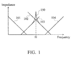
- FIG. 1 is a diagram showing an exemplary impedance profile of a system.
- the curve 101 represents a first capacitive impedance of a component, such as a printed circuit board (PCB), in the system.
- the curve 102 represents a second capacitive impedance of a component, such as a die, in the system.
- the curve 103 represents a first inductive impedance of a component, such as the PCB, in the system.
- the curve 104 represents a second inductive impedance of a component, such as the die, in the system.
- the anti-resonance phenomenon occurs at the particular frequency and a shoulder 105 in the impedance profile is generated. Because the impedance increases enormously at the anti-resonant frequency f1, an undesired amplitude drop in the signal oscillating at the anti-resonant frequency f1 will occur and cause the performance of the system to suffer.
- An exemplary embodiment of a semiconductor integrated circuit device comprises a chip main circuit, a damper and a passive component.
- the chip main circuit is coupled to a power source and performs a predetermined function.
- the damper is coupled to an output terminal of the chip main circuit.
- the passive component is coupled to the chip main circuit via the damper.
- An exemplary embodiment of a semiconductor integrated circuit device comprises a chip main circuit and a damper.
- the chip main circuit is coupled to a power source and performs a predetermined function.
- the damper is coupled to an output terminal of the chip main circuit.
- the damper is coupled between the chip main circuit and a passive component for suppressing anti-resonance of the semiconductor integrated circuit device.
- FIG. 2 shows an exemplary block diagram of a semiconductor integrated circuit device according to an embodiment of the invention.
- the semiconductor integrated circuit device 200 may at least comprise a chip main circuit 210 and a damper 220.
- the chip main circuit 210 is coupled to a power source 240 and performs a predetermined function.
- the chip main circuit 210 may perform a modem (that is, modulation and demodulation) function for wired/wireless communication, a signal processing function for wired/wireless communication, a digital signal processing function, an analog signal processing function, etc.
- modem that is, modulation and demodulation
- the chip main circuit 210 may be integrated in a chip such as a modem chip, a baseband signal processing chip, an RF signal processing chip, a digital signal processing chip, an analog signal processing chip, etc.
- the power source 240 may be configured inside or outside of the chip. In addition, the power source 240 may be configured inside or outside of the chip main circuit 210.
- the damper 220 is coupled to an output terminal OUT of the chip main circuit 210.
- the semiconductor integrated circuit device 200 may further comprise a passive component 230.
- the damper 220 is coupled between the chip main circuit 210 and the passive component 230.
- the passive component 230 is coupled to the chip main circuit 210 via the damper 220.
- the passive component 230 is in an independent path that is not directly connected to the power source 240, regardless of whether the power source 240 is configured inside or outside of the chip main circuit 210 or the chip.
- the damper 220 is coupled between the chip main circuit 210 and the passive component 220 for suppressing anti-resonance of the semiconductor integrated circuit device 200.
- the damper 220 and the passive component 230 are the circuit components external to the chip main circuit 210, as shown in FIG. 2 .
- the predetermined function performed by the chip main circuit 210 is not affected by the damper 220 and the passive component 230.
- the chip main circuit 210 can perform the predetermined function even if the damper 220 and the passive component 230 are not coupled thereto or do not even exist in the semiconductor integrated circuit device 200.
- the damper 220 and the passive component 230 are introduced to decrease the impedance and suppress anti-resonance of the semiconductor integrated circuit device 200.
- the chip main circuit 210, the damper 220 and the passive component 230 may be packed in a package and/or mounted on a printed circuit board (PCB). Therefore, in some embodiments of the invention, the semiconductor integrated circuit device 200 may further comprise a package and/or a PCB.
- PCB printed circuit board
- FIG. 3 is an equivalent circuit diagram of an electronic system comprising the semiconductor integrated circuit device according to an embodiment of the invention.
- the capacitor Cpcb represents the equivalent capacitor of the PCB.
- the inductor Lpcb represents the equivalent inductor of the PCB.
- the resistor Rpkg represents the equivalent resistor of the package.
- the inductor Lpkg represents the equivalent inductor of the package.
- the resistor Rdie represents the equivalent resistor of a chip with the chip main circuit 210 integrated therein.
- the capacitor Cdie represents the equivalent capacitor of the chip with the chip main circuit 210 integrated therein.
- the capacitor Cext represents the equivalent capacitor of the passive component 230.
- the inductor Lext represents the parasitic inductor of the passive component 230.
- the resistor Rext represents the parasitic resistor of the passive component 230.
- the resistor Rvar represents the equivalent resistor of the damper 220.
- the capacitor Cext, the inductor Lext and the resistor Rext may be as a whole regarded as the overall impedance contributed by the passive component 230.
- the damper 220 and the passive component 230 are coupled in serial.
- the passive component 230 is not directly connected to the power source Vsys of the electronic system and is coupled to the chip (that is, the chip main circuit 210) via the damper 220.
- the resistance of the damper 220 may be adjustable, so as to be adjusted to an optimal value for suppressing anti-resonance of the semiconductor integrated circuit device 200.
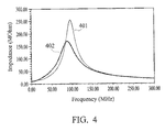
- FIG. 4 is a diagram showing exemplary impedance profiles of the electronic system according to an embodiment of the invention.
- FIG. 4 shows the impedance profiles of the shoulder generated when anti-resonance occurs.
- the curve 401 represents the impedance profile of the shoulder when the damper 220 is not added.
- the curve 402 represents the impedance profile of the shoulder when the damper 220 is added to the electronic system as shown in FIG. 2 and FIG. 3 .
- the shoulder becomes wider and the peak amplitude of the shoulder is decreased.
- the damper 220 is a variable resistor.
- the resistance of the resistor may be adjusted to an optimal value for suppressing anti-resonance of the semiconductor integrated circuit device 200.
- the passive component 230 is a capacitor.
- FIG. 5A shows an exemplary circuit diagram of a semiconductor integrated circuit device according to an embodiment of the invention.
- the variable resistor 520 is coupled between the chip main circuit 510 and the capacitor 530.
- the capacitor 530 may be regarded as an external decoupling capacitor of the chip main circuit 510.
- the semiconductor integrated circuit device 500 may further comprise a control circuit 550 generating a multi-bit control signal Control_Bit for controlling the resistance of the variable resistor 520 (that is, the damper).
- the control circuit 550 may also be integrated in the chip main circuit 510, or may be implemented by any device in the chip main circuit 510. Therefore, the invention should not be limited to the architecture shown in FIG. 5A .
- the variable resistor 520 may be implemented by a plurality of transistors coupled in parallel.
- the variable resistor may be implemented by four transistors with a first electrode coupled to the terminal X, a second electrode coupled to the terminal Y and a control electrode receiving the corresponding control signal B1 ⁇ B4 carried in the multi-bit control signal Control_Bit.
- the transistor When the transistor is turned on in response to the corresponding control signal, the transistor is equivalent to a resistor or resistive device.
- the multi-bit control signal [0000] may correspond to the minimum resistance provided by the variable resistor 520
- the multi-bit control signal [1110] may correspond to the maximum resistance provided by the variable resistor 520.
- variable resistor may also be implemented by less than or more than four transistors, resistive devices, resistors, or inductors.
- the chip main circuit 510 may comprise a processor 511.
- the processor 511 may determine the optimal resistance of the variable resistor 520 (that is, the damper) by searching for the minimum system voltage provided by the power source (such as the power source 240 or Vsys) of the electronic system for the chip main circuit 510, the semiconductor integrated circuit device, or even the electronic system being able to function without crashing, and generate a control signal for controlling the resistance of the variable resistor 520 (that is, the damper) according to the optimal resistance.
- the control signal may be provide to the control circuit 550 and the control circuit 550 generates the multi-bit control signal Control_Bit according to the control signal as shown in FIG. 5 , or may be directly provided to the variable resistor 520 for controlling the resistance thereof.
- the processor 511 may first search for a corresponding minimum system voltage, such as Vmin_R1, Vmin_R2...Vmin_Rn, provided by the power source of the electronic system for the chip main circuit 510, the semiconductor integrated circuit device, or even the electronic system to be able to function without crashing, and then compare the minimum system voltages Vmin_R1, Vmin_R2...Vmin_Rn to obtain the smallest one among them.
- the resistance corresponding to the smallest one may be determined to be the optimal resistance.
- FIG. 6 is a flow chart of a method for determining the optimal resistance of the damper according to an embodiment of the invention.
- the chip main circuit boots up and the processor generates control signals to control the resistance of the damper (for example, the variable resistor).
- the system voltage provided by the power source is adjusted to multiple levels as well for every possible resistance supported by the damper, to test whether the electronic system can function normally or not under each level of system voltage, and obtain the minimum system voltage that the electronic system is able to function on without crashing, corresponding to each resistance supported by the damper (Step S604).
- the processor obtains the smallest of the minimum system voltages corresponding to the supported resistance (Step S606).
- the resistance corresponding to the smallest one is determined to be the optimal resistance.
- the processor generates a control signal for setting the resistance of the damper to the optimal resistance (Step S608).
- the chip main circuit, the damper and the passive component may be integrated in a chip.
- FIG. 7 shows an exemplary lateral view of an electronic system according to an embodiment of the invention.
- the chip main circuit, the damper (for example, a variable resistor) and the passive component (for example, an external decoupling capacitor) may be integrated in a chip 700.
- the chip 700 may be packed in the substrate as shown.
- the chip main circuit and the damper may be integrated in a chip, and the passive component may be configured outside of the chip.
- FIG. 8 shows an exemplary lateral view of an electronic system according to another embodiment of the invention.
- the chip main circuit and the damper for example, a variable resistor
- the passive component for example, an external decoupling capacitor
- the chip 800 may be packed in the substrate as shown, and the passive component may be coupled to the damper via a trace.
- the chip main circuit may be integrated in a chip, and the damper and the passive component may be configured outside of the chip.
- FIG. 9 shows an exemplary lateral view of an electronic system according to another embodiment of the invention.
- the chip main circuit may be integrated in a chip 900, and the damper (for example, a variable resistor) and the passive component (for example, an external decoupling capacitor) may be configured outside of the chip 900.
- the chip 900 may be packed in the substrate as shown, and the damper and the passive component may be coupled to the damper via a trace.
- the damper and the passive component may also be integrated as one device, and the invention should not be limited to the embodiments as illustrated above.
- the damper for example, a variable resistor
- the passive component for example, an external decoupling capacitor
- the impedance and the anti-resonance of the semiconductor integrated circuit device or the electronic system can be effectively decreased and suppressed.
Landscapes
- Physics & Mathematics (AREA)
- Nonlinear Science (AREA)
- Engineering & Computer Science (AREA)
- Manufacturing & Machinery (AREA)
- Semiconductor Integrated Circuits (AREA)
Abstract
Description
- The invention relates to a semiconductor integrated circuit device, and more particularly to a semiconductor integrated circuit device with a tunable external decoupling capacitor for anti-resonance suppression.
- Anti-resonance is a pronounced minimum in the amplitude of a circuit at a particular frequency, accompanied by a large shift in its oscillation phase. Such a frequency is known as the system's anti-resonant frequency, and at this frequency, the amplitude of a signal can drop to almost zero.
-
FIG. 1 is a diagram showing an exemplary impedance profile of a system. Thecurve 101 represents a first capacitive impedance of a component, such as a printed circuit board (PCB), in the system. Thecurve 102 represents a second capacitive impedance of a component, such as a die, in the system. Thecurve 103 represents a first inductive impedance of a component, such as the PCB, in the system. Thecurve 104 represents a second inductive impedance of a component, such as the die, in the system. - When two curves intersect at a particular frequency, such as the frequency fl shown in
FIG. 1 , the anti-resonance phenomenon occurs at the particular frequency and a shoulder 105 in the impedance profile is generated. Because the impedance increases enormously at the anti-resonant frequency f1, an undesired amplitude drop in the signal oscillating at the anti-resonant frequency f1 will occur and cause the performance of the system to suffer. - To suppress the undesired anti-resonance, a novel design for a semiconductor integrated circuit device is required.
- Semiconductor integrated circuit devices are provided. An exemplary embodiment of a semiconductor integrated circuit device comprises a chip main circuit, a damper and a passive component. The chip main circuit is coupled to a power source and performs a predetermined function. The damper is coupled to an output terminal of the chip main circuit. The passive component is coupled to the chip main circuit via the damper.
- An exemplary embodiment of a semiconductor integrated circuit device comprises a chip main circuit and a damper. The chip main circuit is coupled to a power source and performs a predetermined function. The damper is coupled to an output terminal of the chip main circuit. The damper is coupled between the chip main circuit and a passive component for suppressing anti-resonance of the semiconductor integrated circuit device.
- A detailed description is given in the following embodiments with reference to the accompanying drawings.
- The invention can be more fully understood by reading the subsequent detailed description and examples with references made to the accompanying drawings, wherein:
-
FIG. 1 is a diagram showing an exemplary impedance profile of a system; -
FIG. 2 shows an exemplary block diagram of a semiconductor integrated circuit device according to an embodiment of the invention; -
FIG. 3 is an equivalent circuit diagram of an electronic system comprising the semiconductor integrated circuit device according to an embodiment of the invention; -
FIG. 4 is a diagram showing an exemplary impedance profiles of the electronic system according to an embodiment of the invention; -
FIG. 5A shows an exemplary circuit diagram of a semiconductor integrated circuit device according to an embodiment of the invention; -
FIG. 5B shows an exemplary circuit diagram of a variable resistor according to an embodiment of the invention; -
FIG. 6 is a flow chart of a method for determining the optimal resistance of the damper according to an embodiment of the invention; -
FIG. 7 shows an exemplary lateral view of an electronic system according to an embodiment of the invention; -
FIG. 8 shows an exemplary lateral view of an electronic system according to another embodiment of the invention; and -
FIG. 9 shows an exemplary lateral view of an electronic system according to another embodiment of the invention. - The following description is of the best-contemplated mode of carrying out the invention. This description is made for the purpose of illustrating the general principles of the invention and should not be taken in a limiting sense. The scope of the invention is best determined by reference to the appended claims.
-
FIG. 2 shows an exemplary block diagram of a semiconductor integrated circuit device according to an embodiment of the invention. The semiconductor integratedcircuit device 200 may at least comprise a chipmain circuit 210 and adamper 220. The chipmain circuit 210 is coupled to apower source 240 and performs a predetermined function. For example, the chipmain circuit 210 may perform a modem (that is, modulation and demodulation) function for wired/wireless communication, a signal processing function for wired/wireless communication, a digital signal processing function, an analog signal processing function, etc. - For providing the predetermined function, the chip
main circuit 210 may be integrated in a chip such as a modem chip, a baseband signal processing chip, an RF signal processing chip, a digital signal processing chip, an analog signal processing chip, etc. Thepower source 240 may be configured inside or outside of the chip. In addition, thepower source 240 may be configured inside or outside of the chipmain circuit 210. - The
damper 220 is coupled to an output terminal OUT of the chipmain circuit 210. - The semiconductor
integrated circuit device 200 may further comprise apassive component 230. Thedamper 220 is coupled between the chipmain circuit 210 and thepassive component 230. In other words, in an embodiment of the invention, thepassive component 230 is coupled to the chipmain circuit 210 via thedamper 220. - According to an embodiment of the invention, the
passive component 230 is in an independent path that is not directly connected to thepower source 240, regardless of whether thepower source 240 is configured inside or outside of the chipmain circuit 210 or the chip. - In addition, according to an embodiment of the invention, the
damper 220 is coupled between the chipmain circuit 210 and thepassive component 220 for suppressing anti-resonance of the semiconductor integratedcircuit device 200. - In addition, in the embodiments of the invention, the
damper 220 and thepassive component 230 are the circuit components external to the chipmain circuit 210, as shown inFIG. 2 . In other words, the predetermined function performed by the chipmain circuit 210 is not affected by thedamper 220 and thepassive component 230. The chipmain circuit 210 can perform the predetermined function even if thedamper 220 and thepassive component 230 are not coupled thereto or do not even exist in the semiconductor integratedcircuit device 200. Thedamper 220 and thepassive component 230 are introduced to decrease the impedance and suppress anti-resonance of the semiconductor integratedcircuit device 200. - According to an embodiment of the invention, the chip
main circuit 210, thedamper 220 and thepassive component 230 may be packed in a package and/or mounted on a printed circuit board (PCB). Therefore, in some embodiments of the invention, the semiconductor integratedcircuit device 200 may further comprise a package and/or a PCB. -
FIG. 3 is an equivalent circuit diagram of an electronic system comprising the semiconductor integrated circuit device according to an embodiment of the invention. The capacitor Cpcb represents the equivalent capacitor of the PCB. The inductor Lpcb represents the equivalent inductor of the PCB. The resistor Rpkg represents the equivalent resistor of the package. The inductor Lpkg represents the equivalent inductor of the package. The resistor Rdie represents the equivalent resistor of a chip with the chipmain circuit 210 integrated therein. The capacitor Cdie represents the equivalent capacitor of the chip with the chipmain circuit 210 integrated therein. - The capacitor Cext represents the equivalent capacitor of the
passive component 230. The inductor Lext represents the parasitic inductor of thepassive component 230. The resistor Rext represents the parasitic resistor of thepassive component 230. The resistor Rvar represents the equivalent resistor of thedamper 220. - The capacitor Cext, the inductor Lext and the resistor Rext may be as a whole regarded as the overall impedance contributed by the
passive component 230. According to an embodiment of the invention, thedamper 220 and thepassive component 230 are coupled in serial. - As shown in
FIG. 3 , thepassive component 230 is not directly connected to the power source Vsys of the electronic system and is coupled to the chip (that is, the chip main circuit 210) via thedamper 220. - According to an embodiment of the invention, the resistance of the
damper 220 may be adjustable, so as to be adjusted to an optimal value for suppressing anti-resonance of the semiconductor integratedcircuit device 200. -
FIG. 4 is a diagram showing exemplary impedance profiles of the electronic system according to an embodiment of the invention.FIG. 4 shows the impedance profiles of the shoulder generated when anti-resonance occurs. Thecurve 401 represents the impedance profile of the shoulder when thedamper 220 is not added. Thecurve 402 represents the impedance profile of the shoulder when thedamper 220 is added to the electronic system as shown inFIG. 2 andFIG. 3 . As shown inFIG. 4 , when thedamper 220 is added, the shoulder becomes wider and the peak amplitude of the shoulder is decreased. - According to an embodiment of the invention, the
damper 220 is a variable resistor. The resistance of the resistor may be adjusted to an optimal value for suppressing anti-resonance of the semiconductor integratedcircuit device 200. - According to an embodiment of the invention, the
passive component 230 is a capacitor. -
FIG. 5A shows an exemplary circuit diagram of a semiconductor integrated circuit device according to an embodiment of the invention. Thevariable resistor 520 is coupled between the chipmain circuit 510 and thecapacitor 530. Thecapacitor 530 may be regarded as an external decoupling capacitor of the chipmain circuit 510. The semiconductor integratedcircuit device 500 may further comprise acontrol circuit 550 generating a multi-bit control signal Control_Bit for controlling the resistance of the variable resistor 520 (that is, the damper). Note that in some embodiments, thecontrol circuit 550 may also be integrated in the chipmain circuit 510, or may be implemented by any device in the chipmain circuit 510. Therefore, the invention should not be limited to the architecture shown inFIG. 5A . - In the embodiment, the
variable resistor 520 may be implemented by a plurality of transistors coupled in parallel. For example, as an exemplary circuit diagram shown inFIG. 5B , the variable resistor may be implemented by four transistors with a first electrode coupled to the terminal X, a second electrode coupled to the terminal Y and a control electrode receiving the corresponding control signal B1∼B4 carried in the multi-bit control signal Control_Bit. When the transistor is turned on in response to the corresponding control signal, the transistor is equivalent to a resistor or resistive device. For example, the multi-bit control signal [0000] may correspond to the minimum resistance provided by thevariable resistor 520, and the multi-bit control signal [1110] may correspond to the maximum resistance provided by thevariable resistor 520. - Note that, although there are four transistors or resistive devices shown in
FIG. 5B to implement the variable resistor, the invention should not be limited thereto. The variable resistor may also be implemented by less than or more than four transistors, resistive devices, resistors, or inductors. - According to an embodiment of the invention, the chip
main circuit 510 may comprise aprocessor 511. Theprocessor 511 may determine the optimal resistance of the variable resistor 520 (that is, the damper) by searching for the minimum system voltage provided by the power source (such as thepower source 240 or Vsys) of the electronic system for the chipmain circuit 510, the semiconductor integrated circuit device, or even the electronic system being able to function without crashing, and generate a control signal for controlling the resistance of the variable resistor 520 (that is, the damper) according to the optimal resistance. The control signal may be provide to thecontrol circuit 550 and thecontrol circuit 550 generates the multi-bit control signal Control_Bit according to the control signal as shown inFIG. 5 , or may be directly provided to thevariable resistor 520 for controlling the resistance thereof. - For example, in an embodiment of the invention, suppose that there are n values of resistance R1-Rn that can be provided by the
variable resistor 520. For each resistance, theprocessor 511 may first search for a corresponding minimum system voltage, such as Vmin_R1, Vmin_R2...Vmin_Rn, provided by the power source of the electronic system for the chipmain circuit 510, the semiconductor integrated circuit device, or even the electronic system to be able to function without crashing, and then compare the minimum system voltages Vmin_R1, Vmin_R2...Vmin_Rn to obtain the smallest one among them. The resistance corresponding to the smallest one may be determined to be the optimal resistance. -
FIG. 6 is a flow chart of a method for determining the optimal resistance of the damper according to an embodiment of the invention. When the electronic system powers on (that is, when the power source supplies power) (Step S602), the chip main circuit boots up and the processor generates control signals to control the resistance of the damper (for example, the variable resistor). The system voltage provided by the power source is adjusted to multiple levels as well for every possible resistance supported by the damper, to test whether the electronic system can function normally or not under each level of system voltage, and obtain the minimum system voltage that the electronic system is able to function on without crashing, corresponding to each resistance supported by the damper (Step S604). Next, the processor obtains the smallest of the minimum system voltages corresponding to the supported resistance (Step S606). The resistance corresponding to the smallest one is determined to be the optimal resistance. Next, the processor generates a control signal for setting the resistance of the damper to the optimal resistance (Step S608). - According to an embodiment of the invention, the chip main circuit, the damper and the passive component may be integrated in a chip.
-
FIG. 7 shows an exemplary lateral view of an electronic system according to an embodiment of the invention. In this embodiment, the chip main circuit, the damper (for example, a variable resistor) and the passive component (for example, an external decoupling capacitor) may be integrated in achip 700. Thechip 700 may be packed in the substrate as shown. - According to another embodiment of the invention, the chip main circuit and the damper may be integrated in a chip, and the passive component may be configured outside of the chip.
-
FIG. 8 shows an exemplary lateral view of an electronic system according to another embodiment of the invention. In this embodiment, the chip main circuit and the damper (for example, a variable resistor) may be integrated in achip 800, and the passive component (for example, an external decoupling capacitor) may be configured outside of thechip 800. Thechip 800 may be packed in the substrate as shown, and the passive component may be coupled to the damper via a trace. - According to yet another embodiment of the invention, the chip main circuit may be integrated in a chip, and the damper and the passive component may be configured outside of the chip.
-
FIG. 9 shows an exemplary lateral view of an electronic system according to another embodiment of the invention. In this embodiment, the chip main circuit may be integrated in achip 900, and the damper (for example, a variable resistor) and the passive component (for example, an external decoupling capacitor) may be configured outside of thechip 900. Thechip 900 may be packed in the substrate as shown, and the damper and the passive component may be coupled to the damper via a trace. - Note that, in some embodiments of the invention, the damper and the passive component may also be integrated as one device, and the invention should not be limited to the embodiments as illustrated above. For example, the damper (for example, a variable resistor) may be implemented in the passive component (for example, an external decoupling capacitor).
- As described above, in the embodiments of the invention, with the
damper 220 and thepassive component 230, the impedance and the anti-resonance of the semiconductor integrated circuit device or the electronic system can be effectively decreased and suppressed. - While the invention has been described by way of example and in terms of preferred embodiment, it is to be understood that the invention is not limited thereto. Those who are skilled in this technology can still make various alterations and modifications without departing from the scope and spirit of this invention. Therefore, the scope of the present invention shall be defined and protected by the following claims and their equivalents.
Claims (12)
Applications Claiming Priority (2)
| Application Number | Priority Date | Filing Date | Title |
|---|---|---|---|
| US201562241240P | 2015-10-14 | 2015-10-14 | |
| US15/274,473 US10581414B2 (en) | 2015-10-14 | 2016-09-23 | Semiconductor integrated circuit device |
Publications (2)
| Publication Number | Publication Date |
|---|---|
| EP3163616A1 true EP3163616A1 (en) | 2017-05-03 |
| EP3163616B1 EP3163616B1 (en) | 2019-12-04 |
Family
ID=57199884
Family Applications (1)
| Application Number | Title | Priority Date | Filing Date |
|---|---|---|---|
| EP16192005.3A Active EP3163616B1 (en) | 2015-10-14 | 2016-10-03 | Semiconductor integrated circuit device |
Country Status (4)
| Country | Link |
|---|---|
| US (1) | US10581414B2 (en) |
| EP (1) | EP3163616B1 (en) |
| CN (1) | CN107017855A (en) |
| TW (1) | TW201714404A (en) |
Families Citing this family (1)
| Publication number | Priority date | Publication date | Assignee | Title |
|---|---|---|---|---|
| US11430797B2 (en) * | 2020-06-30 | 2022-08-30 | Qualcomm Incorporated | Package embedded programmable resistor for voltage droop mitigation |
Citations (6)
| Publication number | Priority date | Publication date | Assignee | Title |
|---|---|---|---|---|
| JPS6175558A (en) * | 1984-09-21 | 1986-04-17 | Nec Corp | Hybrid integrated circuit device |
| US20060139123A1 (en) * | 2004-12-29 | 2006-06-29 | Lsi Logic Corporation | Resistive capacitor structure for anti-resonance reduction |
| US20070279882A1 (en) * | 2006-06-06 | 2007-12-06 | Samtec, Inc. | Power distribution system for integrated circuits |
| US20110180898A1 (en) * | 2010-01-27 | 2011-07-28 | Kabushiki Kaisha Toshiba | Semiconductor device |
| US20120081193A1 (en) * | 2010-09-30 | 2012-04-05 | Denso Corporation | Band elimination filter providing attenuation within wide range of frequencies |
| US20150207485A1 (en) * | 2014-01-20 | 2015-07-23 | Yen Wei Hsu | RC network |
Family Cites Families (10)
| Publication number | Priority date | Publication date | Assignee | Title |
|---|---|---|---|---|
| US5543756A (en) * | 1995-05-12 | 1996-08-06 | Hewlett-Packard Company | Combined crystal and LC filter |
| US6700390B2 (en) * | 2002-05-31 | 2004-03-02 | Sun Microsystems, Inc. | Adjustment and calibration system to store resistance settings to control chip/package resonance |
| US7839233B2 (en) * | 2008-01-23 | 2010-11-23 | Analog Devices, Inc. | Attenuator |
| US8952792B1 (en) * | 2011-01-07 | 2015-02-10 | Impinj, Inc. | Self tuning RFID tags |
| JP5691670B2 (en) * | 2011-03-09 | 2015-04-01 | 日本電気株式会社 | Power supply control system and power supply control method for semiconductor integrated circuit |
| TWI423557B (en) | 2011-05-11 | 2014-01-11 | 廣達電腦股份有限公司 | Electronic product using rechargeable battery and battery state control method thereof |
| WO2013073591A1 (en) * | 2011-11-14 | 2013-05-23 | 日本電気株式会社 | Decoupling circuit and semiconductor integrated circuit |
| JP6169395B2 (en) * | 2012-08-27 | 2017-07-26 | 株式会社トーキン | Resonator |
| US9377804B2 (en) * | 2014-04-10 | 2016-06-28 | Qualcomm Incorporated | Switchable package capacitor for charge conservation and series resistance |
| CN105956289B (en) * | 2016-05-06 | 2018-11-30 | 西安电子科技大学 | Power distribution network design method based on decoupling capacitor decoupling region |
-
2016
- 2016-09-23 US US15/274,473 patent/US10581414B2/en active Active
- 2016-10-03 EP EP16192005.3A patent/EP3163616B1/en active Active
- 2016-10-03 TW TW105131867A patent/TW201714404A/en unknown
- 2016-10-11 CN CN201610884179.0A patent/CN107017855A/en not_active Withdrawn
Patent Citations (6)
| Publication number | Priority date | Publication date | Assignee | Title |
|---|---|---|---|---|
| JPS6175558A (en) * | 1984-09-21 | 1986-04-17 | Nec Corp | Hybrid integrated circuit device |
| US20060139123A1 (en) * | 2004-12-29 | 2006-06-29 | Lsi Logic Corporation | Resistive capacitor structure for anti-resonance reduction |
| US20070279882A1 (en) * | 2006-06-06 | 2007-12-06 | Samtec, Inc. | Power distribution system for integrated circuits |
| US20110180898A1 (en) * | 2010-01-27 | 2011-07-28 | Kabushiki Kaisha Toshiba | Semiconductor device |
| US20120081193A1 (en) * | 2010-09-30 | 2012-04-05 | Denso Corporation | Band elimination filter providing attenuation within wide range of frequencies |
| US20150207485A1 (en) * | 2014-01-20 | 2015-07-23 | Yen Wei Hsu | RC network |
Also Published As
| Publication number | Publication date |
|---|---|
| EP3163616B1 (en) | 2019-12-04 |
| TW201714404A (en) | 2017-04-16 |
| US10581414B2 (en) | 2020-03-03 |
| US20170111032A1 (en) | 2017-04-20 |
| CN107017855A (en) | 2017-08-04 |
Similar Documents
| Publication | Publication Date | Title |
|---|---|---|
| US9584097B2 (en) | System and method for a switchable capacitance | |
| JP6533251B2 (en) | Method and apparatus for use in digitally tuning a capacitor in an integrated circuit device | |
| EP2651032B1 (en) | Tunable capacitor | |
| CN104184452B (en) | Data conversion device, digital transmission device and digital conversion method | |
| KR101659651B1 (en) | System and method for a switchable capacitance | |
| US7701277B2 (en) | Variable-impedance gated decoupling cell | |
| US9281781B2 (en) | Semiconductor apparatus, oscillation circuit, and signal processing system | |
| US20140368249A1 (en) | Delay control circuit | |
| JP2018032951A (en) | Power Amplifier Module | |
| US10581414B2 (en) | Semiconductor integrated circuit device | |
| US7915967B2 (en) | Frequency-tunable oscillator arrangement | |
| US20070076498A1 (en) | Controlling circuit for automatically adjusting clock frequency of a central processing unit | |
| US20090212853A1 (en) | Apparatus for supplying power in semiconductor integrated circuit and input impedance control method of the same | |
| US10840894B1 (en) | Linear delay generation circuitry and method | |
| US9297840B2 (en) | Power detection circuit | |
| KR101517389B1 (en) | Resistor-capacitor auto calibration system and calibration method therefor | |
| US20180159581A1 (en) | Signal processing apparatus | |
| US20150061753A1 (en) | Signal output circuit and signal output method | |
| US10630237B2 (en) | High-voltage standing-wave oscillator | |
| JP2016096497A (en) | Equalizer circuit and semiconductor integrated device | |
| US20170264259A1 (en) | Integrated circuitry | |
| US7205856B2 (en) | Piezoelectric oscillator | |
| US20110163612A1 (en) | Load devices with linearization technique employed therein | |
| US7646211B2 (en) | Circuit and apparatus for reducing interference of digital signals | |
| JP6031789B2 (en) | Circuit device, oscillation device, and electronic device |
Legal Events
| Date | Code | Title | Description |
|---|---|---|---|
| PUAI | Public reference made under article 153(3) epc to a published international application that has entered the european phase |
Free format text: ORIGINAL CODE: 0009012 |
|
| STAA | Information on the status of an ep patent application or granted ep patent |
Free format text: STATUS: THE APPLICATION HAS BEEN PUBLISHED |
|
| AK | Designated contracting states |
Kind code of ref document: A1 Designated state(s): AL AT BE BG CH CY CZ DE DK EE ES FI FR GB GR HR HU IE IS IT LI LT LU LV MC MK MT NL NO PL PT RO RS SE SI SK SM TR |
|
| AX | Request for extension of the european patent |
Extension state: BA ME |
|
| STAA | Information on the status of an ep patent application or granted ep patent |
Free format text: STATUS: REQUEST FOR EXAMINATION WAS MADE |
|
| 17P | Request for examination filed |
Effective date: 20171026 |
|
| RBV | Designated contracting states (corrected) |
Designated state(s): AL AT BE BG CH CY CZ DE DK EE ES FI FR GB GR HR HU IE IS IT LI LT LU LV MC MK MT NL NO PL PT RO RS SE SI SK SM TR |
|
| GRAP | Despatch of communication of intention to grant a patent |
Free format text: ORIGINAL CODE: EPIDOSNIGR1 |
|
| STAA | Information on the status of an ep patent application or granted ep patent |
Free format text: STATUS: GRANT OF PATENT IS INTENDED |
|
| RIC1 | Information provided on ipc code assigned before grant |
Ipc: H01L 23/64 20060101ALI20190520BHEP Ipc: H01L 25/16 20060101AFI20190520BHEP Ipc: H03H 7/06 20060101ALI20190520BHEP Ipc: H03K 5/1252 20060101ALI20190520BHEP |
|
| INTG | Intention to grant announced |
Effective date: 20190621 |
|
| GRAS | Grant fee paid |
Free format text: ORIGINAL CODE: EPIDOSNIGR3 |
|
| GRAA | (expected) grant |
Free format text: ORIGINAL CODE: 0009210 |
|
| STAA | Information on the status of an ep patent application or granted ep patent |
Free format text: STATUS: THE PATENT HAS BEEN GRANTED |
|
| AK | Designated contracting states |
Kind code of ref document: B1 Designated state(s): AL AT BE BG CH CY CZ DE DK EE ES FI FR GB GR HR HU IE IS IT LI LT LU LV MC MK MT NL NO PL PT RO RS SE SI SK SM TR |
|
| REG | Reference to a national code |
Ref country code: GB Ref legal event code: FG4D |
|
| REG | Reference to a national code |
Ref country code: CH Ref legal event code: EP |
|
| REG | Reference to a national code |
Ref country code: AT Ref legal event code: REF Ref document number: 1210475 Country of ref document: AT Kind code of ref document: T Effective date: 20191215 |
|
| REG | Reference to a national code |
Ref country code: DE Ref legal event code: R096 Ref document number: 602016025421 Country of ref document: DE |
|
| REG | Reference to a national code |
Ref country code: IE Ref legal event code: FG4D |
|
| REG | Reference to a national code |
Ref country code: NL Ref legal event code: MP Effective date: 20191204 |
|
| REG | Reference to a national code |
Ref country code: LT Ref legal event code: MG4D |
|
| PG25 | Lapsed in a contracting state [announced via postgrant information from national office to epo] |
Ref country code: LT Free format text: LAPSE BECAUSE OF FAILURE TO SUBMIT A TRANSLATION OF THE DESCRIPTION OR TO PAY THE FEE WITHIN THE PRESCRIBED TIME-LIMIT Effective date: 20191204 Ref country code: NO Free format text: LAPSE BECAUSE OF FAILURE TO SUBMIT A TRANSLATION OF THE DESCRIPTION OR TO PAY THE FEE WITHIN THE PRESCRIBED TIME-LIMIT Effective date: 20200304 Ref country code: SE Free format text: LAPSE BECAUSE OF FAILURE TO SUBMIT A TRANSLATION OF THE DESCRIPTION OR TO PAY THE FEE WITHIN THE PRESCRIBED TIME-LIMIT Effective date: 20191204 Ref country code: LV Free format text: LAPSE BECAUSE OF FAILURE TO SUBMIT A TRANSLATION OF THE DESCRIPTION OR TO PAY THE FEE WITHIN THE PRESCRIBED TIME-LIMIT Effective date: 20191204 Ref country code: GR Free format text: LAPSE BECAUSE OF FAILURE TO SUBMIT A TRANSLATION OF THE DESCRIPTION OR TO PAY THE FEE WITHIN THE PRESCRIBED TIME-LIMIT Effective date: 20200305 Ref country code: FI Free format text: LAPSE BECAUSE OF FAILURE TO SUBMIT A TRANSLATION OF THE DESCRIPTION OR TO PAY THE FEE WITHIN THE PRESCRIBED TIME-LIMIT Effective date: 20191204 Ref country code: BG Free format text: LAPSE BECAUSE OF FAILURE TO SUBMIT A TRANSLATION OF THE DESCRIPTION OR TO PAY THE FEE WITHIN THE PRESCRIBED TIME-LIMIT Effective date: 20200304 |
|
| PG25 | Lapsed in a contracting state [announced via postgrant information from national office to epo] |
Ref country code: RS Free format text: LAPSE BECAUSE OF FAILURE TO SUBMIT A TRANSLATION OF THE DESCRIPTION OR TO PAY THE FEE WITHIN THE PRESCRIBED TIME-LIMIT Effective date: 20191204 Ref country code: HR Free format text: LAPSE BECAUSE OF FAILURE TO SUBMIT A TRANSLATION OF THE DESCRIPTION OR TO PAY THE FEE WITHIN THE PRESCRIBED TIME-LIMIT Effective date: 20191204 |
|
| PG25 | Lapsed in a contracting state [announced via postgrant information from national office to epo] |
Ref country code: AL Free format text: LAPSE BECAUSE OF FAILURE TO SUBMIT A TRANSLATION OF THE DESCRIPTION OR TO PAY THE FEE WITHIN THE PRESCRIBED TIME-LIMIT Effective date: 20191204 |
|
| PG25 | Lapsed in a contracting state [announced via postgrant information from national office to epo] |
Ref country code: PT Free format text: LAPSE BECAUSE OF FAILURE TO SUBMIT A TRANSLATION OF THE DESCRIPTION OR TO PAY THE FEE WITHIN THE PRESCRIBED TIME-LIMIT Effective date: 20200429 Ref country code: EE Free format text: LAPSE BECAUSE OF FAILURE TO SUBMIT A TRANSLATION OF THE DESCRIPTION OR TO PAY THE FEE WITHIN THE PRESCRIBED TIME-LIMIT Effective date: 20191204 Ref country code: RO Free format text: LAPSE BECAUSE OF FAILURE TO SUBMIT A TRANSLATION OF THE DESCRIPTION OR TO PAY THE FEE WITHIN THE PRESCRIBED TIME-LIMIT Effective date: 20191204 Ref country code: NL Free format text: LAPSE BECAUSE OF FAILURE TO SUBMIT A TRANSLATION OF THE DESCRIPTION OR TO PAY THE FEE WITHIN THE PRESCRIBED TIME-LIMIT Effective date: 20191204 Ref country code: ES Free format text: LAPSE BECAUSE OF FAILURE TO SUBMIT A TRANSLATION OF THE DESCRIPTION OR TO PAY THE FEE WITHIN THE PRESCRIBED TIME-LIMIT Effective date: 20191204 Ref country code: CZ Free format text: LAPSE BECAUSE OF FAILURE TO SUBMIT A TRANSLATION OF THE DESCRIPTION OR TO PAY THE FEE WITHIN THE PRESCRIBED TIME-LIMIT Effective date: 20191204 |
|
| PG25 | Lapsed in a contracting state [announced via postgrant information from national office to epo] |
Ref country code: IS Free format text: LAPSE BECAUSE OF FAILURE TO SUBMIT A TRANSLATION OF THE DESCRIPTION OR TO PAY THE FEE WITHIN THE PRESCRIBED TIME-LIMIT Effective date: 20200404 Ref country code: SK Free format text: LAPSE BECAUSE OF FAILURE TO SUBMIT A TRANSLATION OF THE DESCRIPTION OR TO PAY THE FEE WITHIN THE PRESCRIBED TIME-LIMIT Effective date: 20191204 Ref country code: SM Free format text: LAPSE BECAUSE OF FAILURE TO SUBMIT A TRANSLATION OF THE DESCRIPTION OR TO PAY THE FEE WITHIN THE PRESCRIBED TIME-LIMIT Effective date: 20191204 |
|
| REG | Reference to a national code |
Ref country code: DE Ref legal event code: R097 Ref document number: 602016025421 Country of ref document: DE |
|
| REG | Reference to a national code |
Ref country code: AT Ref legal event code: MK05 Ref document number: 1210475 Country of ref document: AT Kind code of ref document: T Effective date: 20191204 |
|
| PLBE | No opposition filed within time limit |
Free format text: ORIGINAL CODE: 0009261 |
|
| STAA | Information on the status of an ep patent application or granted ep patent |
Free format text: STATUS: NO OPPOSITION FILED WITHIN TIME LIMIT |
|
| PG25 | Lapsed in a contracting state [announced via postgrant information from national office to epo] |
Ref country code: DK Free format text: LAPSE BECAUSE OF FAILURE TO SUBMIT A TRANSLATION OF THE DESCRIPTION OR TO PAY THE FEE WITHIN THE PRESCRIBED TIME-LIMIT Effective date: 20191204 |
|
| 26N | No opposition filed |
Effective date: 20200907 |
|
| PG25 | Lapsed in a contracting state [announced via postgrant information from national office to epo] |
Ref country code: AT Free format text: LAPSE BECAUSE OF FAILURE TO SUBMIT A TRANSLATION OF THE DESCRIPTION OR TO PAY THE FEE WITHIN THE PRESCRIBED TIME-LIMIT Effective date: 20191204 Ref country code: PL Free format text: LAPSE BECAUSE OF FAILURE TO SUBMIT A TRANSLATION OF THE DESCRIPTION OR TO PAY THE FEE WITHIN THE PRESCRIBED TIME-LIMIT Effective date: 20191204 Ref country code: SI Free format text: LAPSE BECAUSE OF FAILURE TO SUBMIT A TRANSLATION OF THE DESCRIPTION OR TO PAY THE FEE WITHIN THE PRESCRIBED TIME-LIMIT Effective date: 20191204 |
|
| PG25 | Lapsed in a contracting state [announced via postgrant information from national office to epo] |
Ref country code: IT Free format text: LAPSE BECAUSE OF FAILURE TO SUBMIT A TRANSLATION OF THE DESCRIPTION OR TO PAY THE FEE WITHIN THE PRESCRIBED TIME-LIMIT Effective date: 20191204 |
|
| REG | Reference to a national code |
Ref country code: CH Ref legal event code: PL |
|
| PG25 | Lapsed in a contracting state [announced via postgrant information from national office to epo] |
Ref country code: LU Free format text: LAPSE BECAUSE OF NON-PAYMENT OF DUE FEES Effective date: 20201003 Ref country code: MC Free format text: LAPSE BECAUSE OF FAILURE TO SUBMIT A TRANSLATION OF THE DESCRIPTION OR TO PAY THE FEE WITHIN THE PRESCRIBED TIME-LIMIT Effective date: 20191204 |
|
| REG | Reference to a national code |
Ref country code: BE Ref legal event code: MM Effective date: 20201031 |
|
| PG25 | Lapsed in a contracting state [announced via postgrant information from national office to epo] |
Ref country code: LI Free format text: LAPSE BECAUSE OF NON-PAYMENT OF DUE FEES Effective date: 20201031 Ref country code: CH Free format text: LAPSE BECAUSE OF NON-PAYMENT OF DUE FEES Effective date: 20201031 Ref country code: BE Free format text: LAPSE BECAUSE OF NON-PAYMENT OF DUE FEES Effective date: 20201031 |
|
| PG25 | Lapsed in a contracting state [announced via postgrant information from national office to epo] |
Ref country code: IE Free format text: LAPSE BECAUSE OF NON-PAYMENT OF DUE FEES Effective date: 20201003 |
|
| PG25 | Lapsed in a contracting state [announced via postgrant information from national office to epo] |
Ref country code: TR Free format text: LAPSE BECAUSE OF FAILURE TO SUBMIT A TRANSLATION OF THE DESCRIPTION OR TO PAY THE FEE WITHIN THE PRESCRIBED TIME-LIMIT Effective date: 20191204 Ref country code: MT Free format text: LAPSE BECAUSE OF FAILURE TO SUBMIT A TRANSLATION OF THE DESCRIPTION OR TO PAY THE FEE WITHIN THE PRESCRIBED TIME-LIMIT Effective date: 20191204 Ref country code: CY Free format text: LAPSE BECAUSE OF FAILURE TO SUBMIT A TRANSLATION OF THE DESCRIPTION OR TO PAY THE FEE WITHIN THE PRESCRIBED TIME-LIMIT Effective date: 20191204 |
|
| PG25 | Lapsed in a contracting state [announced via postgrant information from national office to epo] |
Ref country code: MK Free format text: LAPSE BECAUSE OF FAILURE TO SUBMIT A TRANSLATION OF THE DESCRIPTION OR TO PAY THE FEE WITHIN THE PRESCRIBED TIME-LIMIT Effective date: 20191204 |
|
| P01 | Opt-out of the competence of the unified patent court (upc) registered |
Effective date: 20230607 |
|
| PGFP | Annual fee paid to national office [announced via postgrant information from national office to epo] |
Ref country code: GB Payment date: 20250814 Year of fee payment: 10 |
|
| PGFP | Annual fee paid to national office [announced via postgrant information from national office to epo] |
Ref country code: FR Payment date: 20250808 Year of fee payment: 10 |
|
| REG | Reference to a national code |
Ref country code: DE Ref legal event code: R079 Ref document number: 602016025421 Country of ref document: DE Free format text: PREVIOUS MAIN CLASS: H01L0025160000 Ipc: H10W0090000000 |
|
| PGFP | Annual fee paid to national office [announced via postgrant information from national office to epo] |
Ref country code: DE Payment date: 20250805 Year of fee payment: 10 |