EP3163610A1 - Semiconductor package with coated bonding wires - Google Patents
Semiconductor package with coated bonding wires Download PDFInfo
- Publication number
- EP3163610A1 EP3163610A1 EP16177470.8A EP16177470A EP3163610A1 EP 3163610 A1 EP3163610 A1 EP 3163610A1 EP 16177470 A EP16177470 A EP 16177470A EP 3163610 A1 EP3163610 A1 EP 3163610A1
- Authority
- EP
- European Patent Office
- Prior art keywords
- bonding wires
- insulating material
- semiconductor package
- top surface
- carrier substrate
- Prior art date
- Legal status (The legal status is an assumption and is not a legal conclusion. Google has not performed a legal analysis and makes no representation as to the accuracy of the status listed.)
- Ceased
Links
Images



Classifications
-
- H—ELECTRICITY
- H10—SEMICONDUCTOR DEVICES; ELECTRIC SOLID-STATE DEVICES NOT OTHERWISE PROVIDED FOR
- H10W—GENERIC PACKAGES, INTERCONNECTIONS, CONNECTORS OR OTHER CONSTRUCTIONAL DETAILS OF DEVICES COVERED BY CLASS H10
- H10W70/00—Package substrates; Interposers; Redistribution layers [RDL]
- H10W70/40—Leadframes
- H10W70/456—Materials
- H10W70/458—Materials of insulating layers on leadframes
-
- H—ELECTRICITY
- H10—SEMICONDUCTOR DEVICES; ELECTRIC SOLID-STATE DEVICES NOT OTHERWISE PROVIDED FOR
- H10W—GENERIC PACKAGES, INTERCONNECTIONS, CONNECTORS OR OTHER CONSTRUCTIONAL DETAILS OF DEVICES COVERED BY CLASS H10
- H10W72/00—Interconnections or connectors in packages
- H10W72/50—Bond wires
-
- H—ELECTRICITY
- H10—SEMICONDUCTOR DEVICES; ELECTRIC SOLID-STATE DEVICES NOT OTHERWISE PROVIDED FOR
- H10W—GENERIC PACKAGES, INTERCONNECTIONS, CONNECTORS OR OTHER CONSTRUCTIONAL DETAILS OF DEVICES COVERED BY CLASS H10
- H10W70/00—Package substrates; Interposers; Redistribution layers [RDL]
- H10W70/01—Manufacture or treatment
- H10W70/04—Manufacture or treatment of leadframes
- H10W70/041—Connecting or disconnecting interconnections to or from leadframes, e.g. connecting bond wires or bumps
-
- H—ELECTRICITY
- H10—SEMICONDUCTOR DEVICES; ELECTRIC SOLID-STATE DEVICES NOT OTHERWISE PROVIDED FOR
- H10W—GENERIC PACKAGES, INTERCONNECTIONS, CONNECTORS OR OTHER CONSTRUCTIONAL DETAILS OF DEVICES COVERED BY CLASS H10
- H10W70/00—Package substrates; Interposers; Redistribution layers [RDL]
- H10W70/01—Manufacture or treatment
- H10W70/05—Manufacture or treatment of insulating or insulated package substrates, or of interposers, or of redistribution layers
- H10W70/093—Connecting or disconnecting other interconnections thereto or therefrom, e.g. connecting bond wires or bumps
-
- H—ELECTRICITY
- H10—SEMICONDUCTOR DEVICES; ELECTRIC SOLID-STATE DEVICES NOT OTHERWISE PROVIDED FOR
- H10W—GENERIC PACKAGES, INTERCONNECTIONS, CONNECTORS OR OTHER CONSTRUCTIONAL DETAILS OF DEVICES COVERED BY CLASS H10
- H10W70/00—Package substrates; Interposers; Redistribution layers [RDL]
- H10W70/40—Leadframes
- H10W70/464—Additional interconnections in combination with leadframes
- H10W70/465—Bumps or wires
-
- H—ELECTRICITY
- H10—SEMICONDUCTOR DEVICES; ELECTRIC SOLID-STATE DEVICES NOT OTHERWISE PROVIDED FOR
- H10W—GENERIC PACKAGES, INTERCONNECTIONS, CONNECTORS OR OTHER CONSTRUCTIONAL DETAILS OF DEVICES COVERED BY CLASS H10
- H10W70/00—Package substrates; Interposers; Redistribution layers [RDL]
- H10W70/60—Insulating or insulated package substrates; Interposers; Redistribution layers
- H10W70/62—Insulating or insulated package substrates; Interposers; Redistribution layers characterised by their interconnections
- H10W70/65—Shapes or dispositions of interconnections
-
- H—ELECTRICITY
- H10—SEMICONDUCTOR DEVICES; ELECTRIC SOLID-STATE DEVICES NOT OTHERWISE PROVIDED FOR
- H10W—GENERIC PACKAGES, INTERCONNECTIONS, CONNECTORS OR OTHER CONSTRUCTIONAL DETAILS OF DEVICES COVERED BY CLASS H10
- H10W70/00—Package substrates; Interposers; Redistribution layers [RDL]
- H10W70/60—Insulating or insulated package substrates; Interposers; Redistribution layers
- H10W70/67—Insulating or insulated package substrates; Interposers; Redistribution layers characterised by their insulating layers or insulating parts
- H10W70/69—Insulating materials thereof
-
- H—ELECTRICITY
- H10—SEMICONDUCTOR DEVICES; ELECTRIC SOLID-STATE DEVICES NOT OTHERWISE PROVIDED FOR
- H10W—GENERIC PACKAGES, INTERCONNECTIONS, CONNECTORS OR OTHER CONSTRUCTIONAL DETAILS OF DEVICES COVERED BY CLASS H10
- H10W74/00—Encapsulations, e.g. protective coatings
- H10W74/01—Manufacture or treatment
-
- H—ELECTRICITY
- H10—SEMICONDUCTOR DEVICES; ELECTRIC SOLID-STATE DEVICES NOT OTHERWISE PROVIDED FOR
- H10W—GENERIC PACKAGES, INTERCONNECTIONS, CONNECTORS OR OTHER CONSTRUCTIONAL DETAILS OF DEVICES COVERED BY CLASS H10
- H10W74/00—Encapsulations, e.g. protective coatings
- H10W74/01—Manufacture or treatment
- H10W74/016—Manufacture or treatment using moulds
-
- H—ELECTRICITY
- H10—SEMICONDUCTOR DEVICES; ELECTRIC SOLID-STATE DEVICES NOT OTHERWISE PROVIDED FOR
- H10W—GENERIC PACKAGES, INTERCONNECTIONS, CONNECTORS OR OTHER CONSTRUCTIONAL DETAILS OF DEVICES COVERED BY CLASS H10
- H10W74/00—Encapsulations, e.g. protective coatings
- H10W74/10—Encapsulations, e.g. protective coatings characterised by their shape or disposition
- H10W74/111—Encapsulations, e.g. protective coatings characterised by their shape or disposition the semiconductor body being completely enclosed
- H10W74/121—Encapsulations, e.g. protective coatings characterised by their shape or disposition the semiconductor body being completely enclosed by multiple encapsulations, e.g. by a thin protective coating and a thick encapsulation
-
- H—ELECTRICITY
- H10—SEMICONDUCTOR DEVICES; ELECTRIC SOLID-STATE DEVICES NOT OTHERWISE PROVIDED FOR
- H10W—GENERIC PACKAGES, INTERCONNECTIONS, CONNECTORS OR OTHER CONSTRUCTIONAL DETAILS OF DEVICES COVERED BY CLASS H10
- H10W74/00—Encapsulations, e.g. protective coatings
- H10W74/10—Encapsulations, e.g. protective coatings characterised by their shape or disposition
- H10W74/131—Encapsulations, e.g. protective coatings characterised by their shape or disposition the semiconductor body being only partially enclosed
-
- H—ELECTRICITY
- H10—SEMICONDUCTOR DEVICES; ELECTRIC SOLID-STATE DEVICES NOT OTHERWISE PROVIDED FOR
- H10W—GENERIC PACKAGES, INTERCONNECTIONS, CONNECTORS OR OTHER CONSTRUCTIONAL DETAILS OF DEVICES COVERED BY CLASS H10
- H10W74/00—Encapsulations, e.g. protective coatings
- H10W74/40—Encapsulations, e.g. protective coatings characterised by their materials
- H10W74/47—Encapsulations, e.g. protective coatings characterised by their materials comprising organic materials, e.g. plastics or resins
-
- H—ELECTRICITY
- H10—SEMICONDUCTOR DEVICES; ELECTRIC SOLID-STATE DEVICES NOT OTHERWISE PROVIDED FOR
- H10W—GENERIC PACKAGES, INTERCONNECTIONS, CONNECTORS OR OTHER CONSTRUCTIONAL DETAILS OF DEVICES COVERED BY CLASS H10
- H10W90/00—Package configurations
- H10W90/701—Package configurations characterised by the relative positions of pads or connectors relative to package parts
-
- H—ELECTRICITY
- H10—SEMICONDUCTOR DEVICES; ELECTRIC SOLID-STATE DEVICES NOT OTHERWISE PROVIDED FOR
- H10W—GENERIC PACKAGES, INTERCONNECTIONS, CONNECTORS OR OTHER CONSTRUCTIONAL DETAILS OF DEVICES COVERED BY CLASS H10
- H10W72/00—Interconnections or connectors in packages
- H10W72/01—Manufacture or treatment
- H10W72/015—Manufacture or treatment of bond wires
- H10W72/01515—Forming coatings
-
- H—ELECTRICITY
- H10—SEMICONDUCTOR DEVICES; ELECTRIC SOLID-STATE DEVICES NOT OTHERWISE PROVIDED FOR
- H10W—GENERIC PACKAGES, INTERCONNECTIONS, CONNECTORS OR OTHER CONSTRUCTIONAL DETAILS OF DEVICES COVERED BY CLASS H10
- H10W72/00—Interconnections or connectors in packages
- H10W72/071—Connecting or disconnecting
- H10W72/075—Connecting or disconnecting of bond wires
-
- H—ELECTRICITY
- H10—SEMICONDUCTOR DEVICES; ELECTRIC SOLID-STATE DEVICES NOT OTHERWISE PROVIDED FOR
- H10W—GENERIC PACKAGES, INTERCONNECTIONS, CONNECTORS OR OTHER CONSTRUCTIONAL DETAILS OF DEVICES COVERED BY CLASS H10
- H10W72/00—Interconnections or connectors in packages
- H10W72/071—Connecting or disconnecting
- H10W72/075—Connecting or disconnecting of bond wires
- H10W72/07551—Connecting or disconnecting of bond wires characterised by changes in properties of the bond wires during the connecting
- H10W72/07553—Connecting or disconnecting of bond wires characterised by changes in properties of the bond wires during the connecting changes in shapes
-
- H—ELECTRICITY
- H10—SEMICONDUCTOR DEVICES; ELECTRIC SOLID-STATE DEVICES NOT OTHERWISE PROVIDED FOR
- H10W—GENERIC PACKAGES, INTERCONNECTIONS, CONNECTORS OR OTHER CONSTRUCTIONAL DETAILS OF DEVICES COVERED BY CLASS H10
- H10W72/00—Interconnections or connectors in packages
- H10W72/30—Die-attach connectors
- H10W72/351—Materials of die-attach connectors
- H10W72/353—Materials of die-attach connectors not comprising solid metals or solid metalloids, e.g. ceramics
- H10W72/354—Materials of die-attach connectors not comprising solid metals or solid metalloids, e.g. ceramics comprising polymers
-
- H—ELECTRICITY
- H10—SEMICONDUCTOR DEVICES; ELECTRIC SOLID-STATE DEVICES NOT OTHERWISE PROVIDED FOR
- H10W—GENERIC PACKAGES, INTERCONNECTIONS, CONNECTORS OR OTHER CONSTRUCTIONAL DETAILS OF DEVICES COVERED BY CLASS H10
- H10W72/00—Interconnections or connectors in packages
- H10W72/50—Bond wires
- H10W72/531—Shapes of wire connectors
- H10W72/537—Multiple bond wires having different shapes
-
- H—ELECTRICITY
- H10—SEMICONDUCTOR DEVICES; ELECTRIC SOLID-STATE DEVICES NOT OTHERWISE PROVIDED FOR
- H10W—GENERIC PACKAGES, INTERCONNECTIONS, CONNECTORS OR OTHER CONSTRUCTIONAL DETAILS OF DEVICES COVERED BY CLASS H10
- H10W72/00—Interconnections or connectors in packages
- H10W72/50—Bond wires
- H10W72/541—Dispositions of bond wires
- H10W72/5445—Dispositions of bond wires being orthogonal to a side surface of the chip, e.g. parallel arrangements
-
- H—ELECTRICITY
- H10—SEMICONDUCTOR DEVICES; ELECTRIC SOLID-STATE DEVICES NOT OTHERWISE PROVIDED FOR
- H10W—GENERIC PACKAGES, INTERCONNECTIONS, CONNECTORS OR OTHER CONSTRUCTIONAL DETAILS OF DEVICES COVERED BY CLASS H10
- H10W72/00—Interconnections or connectors in packages
- H10W72/50—Bond wires
- H10W72/541—Dispositions of bond wires
- H10W72/5449—Dispositions of bond wires not being orthogonal to a side surface of the chip, e.g. fan-out arrangements
-
- H—ELECTRICITY
- H10—SEMICONDUCTOR DEVICES; ELECTRIC SOLID-STATE DEVICES NOT OTHERWISE PROVIDED FOR
- H10W—GENERIC PACKAGES, INTERCONNECTIONS, CONNECTORS OR OTHER CONSTRUCTIONAL DETAILS OF DEVICES COVERED BY CLASS H10
- H10W72/00—Interconnections or connectors in packages
- H10W72/50—Bond wires
- H10W72/551—Materials of bond wires
- H10W72/552—Materials of bond wires comprising metals or metalloids, e.g. silver
-
- H—ELECTRICITY
- H10—SEMICONDUCTOR DEVICES; ELECTRIC SOLID-STATE DEVICES NOT OTHERWISE PROVIDED FOR
- H10W—GENERIC PACKAGES, INTERCONNECTIONS, CONNECTORS OR OTHER CONSTRUCTIONAL DETAILS OF DEVICES COVERED BY CLASS H10
- H10W72/00—Interconnections or connectors in packages
- H10W72/50—Bond wires
- H10W72/551—Materials of bond wires
- H10W72/552—Materials of bond wires comprising metals or metalloids, e.g. silver
- H10W72/5522—Materials of bond wires comprising metals or metalloids, e.g. silver comprising gold [Au]
-
- H—ELECTRICITY
- H10—SEMICONDUCTOR DEVICES; ELECTRIC SOLID-STATE DEVICES NOT OTHERWISE PROVIDED FOR
- H10W—GENERIC PACKAGES, INTERCONNECTIONS, CONNECTORS OR OTHER CONSTRUCTIONAL DETAILS OF DEVICES COVERED BY CLASS H10
- H10W72/00—Interconnections or connectors in packages
- H10W72/50—Bond wires
- H10W72/551—Materials of bond wires
- H10W72/552—Materials of bond wires comprising metals or metalloids, e.g. silver
- H10W72/5525—Materials of bond wires comprising metals or metalloids, e.g. silver comprising copper [Cu]
-
- H—ELECTRICITY
- H10—SEMICONDUCTOR DEVICES; ELECTRIC SOLID-STATE DEVICES NOT OTHERWISE PROVIDED FOR
- H10W—GENERIC PACKAGES, INTERCONNECTIONS, CONNECTORS OR OTHER CONSTRUCTIONAL DETAILS OF DEVICES COVERED BY CLASS H10
- H10W72/00—Interconnections or connectors in packages
- H10W72/50—Bond wires
- H10W72/59—Bond pads specially adapted therefor
-
- H—ELECTRICITY
- H10—SEMICONDUCTOR DEVICES; ELECTRIC SOLID-STATE DEVICES NOT OTHERWISE PROVIDED FOR
- H10W—GENERIC PACKAGES, INTERCONNECTIONS, CONNECTORS OR OTHER CONSTRUCTIONAL DETAILS OF DEVICES COVERED BY CLASS H10
- H10W72/00—Interconnections or connectors in packages
- H10W72/851—Dispositions of multiple connectors or interconnections
- H10W72/874—On different surfaces
- H10W72/884—Die-attach connectors and bond wires
-
- H—ELECTRICITY
- H10—SEMICONDUCTOR DEVICES; ELECTRIC SOLID-STATE DEVICES NOT OTHERWISE PROVIDED FOR
- H10W—GENERIC PACKAGES, INTERCONNECTIONS, CONNECTORS OR OTHER CONSTRUCTIONAL DETAILS OF DEVICES COVERED BY CLASS H10
- H10W74/00—Encapsulations, e.g. protective coatings
-
- H—ELECTRICITY
- H10—SEMICONDUCTOR DEVICES; ELECTRIC SOLID-STATE DEVICES NOT OTHERWISE PROVIDED FOR
- H10W—GENERIC PACKAGES, INTERCONNECTIONS, CONNECTORS OR OTHER CONSTRUCTIONAL DETAILS OF DEVICES COVERED BY CLASS H10
- H10W74/00—Encapsulations, e.g. protective coatings
- H10W74/10—Encapsulations, e.g. protective coatings characterised by their shape or disposition
- H10W74/111—Encapsulations, e.g. protective coatings characterised by their shape or disposition the semiconductor body being completely enclosed
- H10W74/114—Encapsulations, e.g. protective coatings characterised by their shape or disposition the semiconductor body being completely enclosed by a substrate and the encapsulations
-
- H—ELECTRICITY
- H10—SEMICONDUCTOR DEVICES; ELECTRIC SOLID-STATE DEVICES NOT OTHERWISE PROVIDED FOR
- H10W—GENERIC PACKAGES, INTERCONNECTIONS, CONNECTORS OR OTHER CONSTRUCTIONAL DETAILS OF DEVICES COVERED BY CLASS H10
- H10W74/00—Encapsulations, e.g. protective coatings
- H10W74/40—Encapsulations, e.g. protective coatings characterised by their materials
- H10W74/47—Encapsulations, e.g. protective coatings characterised by their materials comprising organic materials, e.g. plastics or resins
- H10W74/473—Encapsulations, e.g. protective coatings characterised by their materials comprising organic materials, e.g. plastics or resins containing a filler
-
- H—ELECTRICITY
- H10—SEMICONDUCTOR DEVICES; ELECTRIC SOLID-STATE DEVICES NOT OTHERWISE PROVIDED FOR
- H10W—GENERIC PACKAGES, INTERCONNECTIONS, CONNECTORS OR OTHER CONSTRUCTIONAL DETAILS OF DEVICES COVERED BY CLASS H10
- H10W90/00—Package configurations
- H10W90/701—Package configurations characterised by the relative positions of pads or connectors relative to package parts
- H10W90/731—Package configurations characterised by the relative positions of pads or connectors relative to package parts of die-attach connectors
- H10W90/734—Package configurations characterised by the relative positions of pads or connectors relative to package parts of die-attach connectors between a chip and a stacked insulating package substrate, interposer or RDL
-
- H—ELECTRICITY
- H10—SEMICONDUCTOR DEVICES; ELECTRIC SOLID-STATE DEVICES NOT OTHERWISE PROVIDED FOR
- H10W—GENERIC PACKAGES, INTERCONNECTIONS, CONNECTORS OR OTHER CONSTRUCTIONAL DETAILS OF DEVICES COVERED BY CLASS H10
- H10W90/00—Package configurations
- H10W90/701—Package configurations characterised by the relative positions of pads or connectors relative to package parts
- H10W90/731—Package configurations characterised by the relative positions of pads or connectors relative to package parts of die-attach connectors
- H10W90/736—Package configurations characterised by the relative positions of pads or connectors relative to package parts of die-attach connectors between a chip and a stacked lead frame, conducting package substrate or heat sink
-
- H—ELECTRICITY
- H10—SEMICONDUCTOR DEVICES; ELECTRIC SOLID-STATE DEVICES NOT OTHERWISE PROVIDED FOR
- H10W—GENERIC PACKAGES, INTERCONNECTIONS, CONNECTORS OR OTHER CONSTRUCTIONAL DETAILS OF DEVICES COVERED BY CLASS H10
- H10W90/00—Package configurations
- H10W90/701—Package configurations characterised by the relative positions of pads or connectors relative to package parts
- H10W90/751—Package configurations characterised by the relative positions of pads or connectors relative to package parts of bond wires
- H10W90/754—Package configurations characterised by the relative positions of pads or connectors relative to package parts of bond wires between a chip and a stacked insulating package substrate, interposer or RDL
-
- H—ELECTRICITY
- H10—SEMICONDUCTOR DEVICES; ELECTRIC SOLID-STATE DEVICES NOT OTHERWISE PROVIDED FOR
- H10W—GENERIC PACKAGES, INTERCONNECTIONS, CONNECTORS OR OTHER CONSTRUCTIONAL DETAILS OF DEVICES COVERED BY CLASS H10
- H10W90/00—Package configurations
- H10W90/701—Package configurations characterised by the relative positions of pads or connectors relative to package parts
- H10W90/751—Package configurations characterised by the relative positions of pads or connectors relative to package parts of bond wires
- H10W90/756—Package configurations characterised by the relative positions of pads or connectors relative to package parts of bond wires between a chip and a stacked lead frame, conducting package substrate or heat sink
Definitions
- the present disclosure relates generally to the field of semiconductor packaging. More particularly, the present disclosure relates to a semiconductor integrated circuit (IC) package with coated bonding wires and a method for making the same.
- IC semiconductor integrated circuit
- the present invention aims at providing an improved semiconductor device and package having insulator-coated bonding wires in order to solve the above-mentioned prior art problems and shortcomings.
- the semiconductor package includes a carrier substrate having a top surface, a semiconductor die mounted on the top surface, a plurality of bonding wires connecting the semiconductor die to the carrier substrate, an insulating material coated on the bonding wires, and a molding compound covering the top surface and encapsulating the semiconductor die, the plurality of bonding wires, and the insulating material.
- the insulating material only covers at least a partial portion of each of the bonding wires.
- the top surface of the carrier substrate is also coated with the insulating material.
- the molding compound comprises an epoxy resin and a filler material
- the insulating material comprises the epoxy resin but without the filler material.
- the insulating material comprises the epoxy resin with a lower content of the filler material.
- a method for forming a semiconductor package is disclosed.
- a carrier substrate having a top surface is provided.
- a semiconductor die is mounted on the top surface.
- a plurality of bonding wires is formed to connect the semiconductor die to the carrier substrate.
- An insulating material is then coated on the bonding wires.
- a molding compound is then formed to encapsulating the semiconductor die, the plurality of bonding wires, and the insulating material.
- a curing process is performed to cure the insulating material.
- the curing process is carried out in an oven or under actinic radiation conditions.
- FIG. 1 is a schematic, cross-sectional diagram showing an exemplary semiconductor package with coated bonding wires according to one embodiment of the invention.
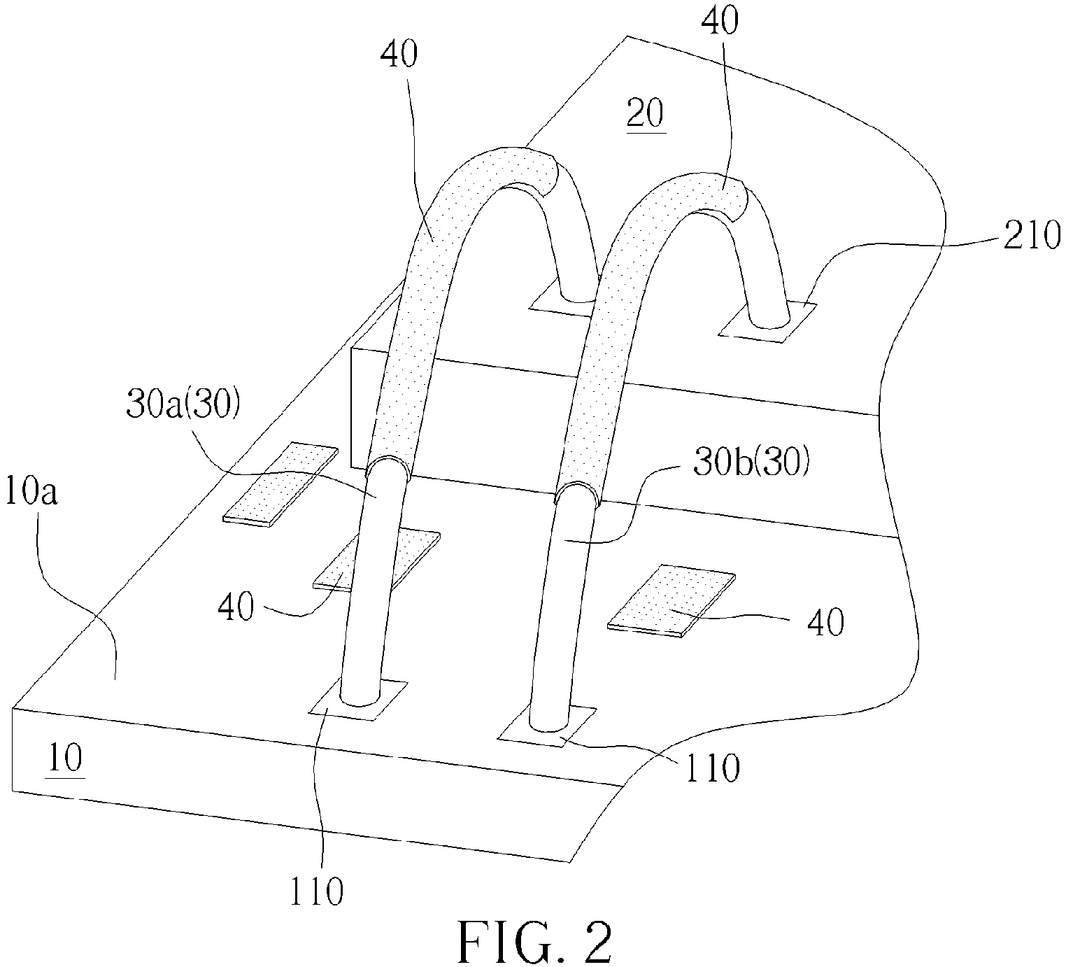
- FIG. 2 is a schematic, perspective view of two adjacent bonding wires in FIG. 1 without the molding compound for clarity.
- the semiconductor package 1 comprises a carrier substrate 10 having a top surface 10a.
- a semiconductor die 20 is mounted on the top surface 10a.
- the semiconductor die 20 has an active surface 20a, on which a plurality of input/output (I/O) pads 210 is distributed.
- the semiconductor die 20 is electrically connected to the bond fingers 110 on the top surface 10a of the carrier substrate 10 through a plurality of bonding wires 30.
- the bonding wires 30 may comprise copper, gold, silver, or any suitable conductive materials.
- the carrier substrate 10 may comprise a packaging substrate, an interposer substrate, or a leadframe substrate, but is not limited thereto.
- the bonding wires 30 are partially coated with an insulating material 40.
- the insulating material 40 may comprise polymers, epoxy, or resins, but is not limited thereto.
- the insulating material 40 coated on the bonding wires 30 may be cured to provide the bonding wires 30 with extra mechanical support.
- the insulating material 40 secures the bonding wires 30 and is able to resist the mold wire sweep during the encapsulation process of the semiconductor package 1.
- the insulating material 40 has low permittivity or low dielectric constant (low-k) that can prevent shorting and alleviate crosstalk between adjacent wires.
- the bonding wires 30 may be fully coated with the insulating material 40 to provide a more desirable isolation effect.
- the semiconductor package 1 further comprises a molding compound 50 on the top surface 10a of the carrier substrate 10.
- the molding compound 50 encapsulates the bonding wires 30, the insulating material 40, and the semiconductor die 20.
- the molding compound 50 may comprise an epoxy resin and a filler material, but is not limited thereto.
- the insulating material 40 may have the same epoxy composition as that of the molding compound 50, but without the filler material or with lower content of the filler material.
- the insulating material 40 contains less than 50ppm halogen content in order to prevent corrosion of the bonding wires 30.
- the insulating material 40 may have a composition that is different from that of the molding compound 50.
- the insulating material 40 is partially coated on the portions of the two adjacent bonding wires 30a and 30b that are most likely to short to the adjacent wires during the wire sweep that occurs during the encapsulation process of the semiconductor package 1.
- the insulating material 40 may be also formed on the top surface 10a of the carrier substrate 10 or elsewhere in the semiconductor package 1.
- the insulating material 40 formed on the top surface 10a of the carrier substrate 10 may enhance the interface adhesive strength between the molding compound 50 and the carrier substrate 10.
- the two adjacent bonding wires 30a and 30b may have different loop heights. It is advantageous to use the present invention because the insulating material 40 coated on the bonding wires 30a and 30b can avoid abnormal wire sweep during encapsulation process and provide significant isolation effect. Furthermore, the loop heights of the two adjacent bonding wires 30a and 30b may be reduced such that more wires can be arranged in the same space.
- FIG. 3 is a schematic, cross-sectional diagram showing the two adjacent bonding wires and the coated insulating material.
- the insulating material 40 may only cover at least a partial portion, for example upper half portion, of each of the bonding wires 30 when viewed in cross-sections of the bonding wires 30.
- the lower half portion of each of the bonding wires 30 is not covered by the insulating material 40.
- each of the bonding wires 30 may be wrapped around by the insulating material 40.
- FIG. 4 to FIG. 7 are schematic, cross-sectional diagrams showing an exemplary method for forming the semiconductor package with coated bonding wires according to one embodiment of the invention, wherein like numeral numbers designate like layers, regions, or elements.
- a semiconductor die 20 is mounted on a top surface 10a of a carrier substrate 10.
- the carrier substrate 10 may comprise a packaging substrate, an interposer substrate, or a leadframe substrate, but is not limited thereto.
- the semiconductor die 20 may be adhered to the top surface 10a by using an adhesive (not explicitly shown), but is not limited thereto.
- the semiconductor die 20 is electrically connected to the bond fingers 110 on the top surface 10a of the carrier substrate 10 through a plurality of bonding wires 30.
- an insulating material 40 is sprayed onto the bonding wires 30 within predetermined regions.
- a region 140 is demonstrated around the semiconductor die 20.
- the insulating material 40 may be sprayed onto the bonding wires 30 within the region 140 that would be most likely to short to the adjacent wires during the encapsulation process.
- the insulating material 40 may be sprayed onto the top surface 10a of the carrier substrate 10 or onto the active surface 20a of the semiconductor die 20, which may enhance the interface adhesive strength between the molding compound and the substrate surface/ die surface. It is understood the region 140 shown in FIG. 8 is for illustration purposes only.
- the insulating material 40 may be sprayed onto the bonding wires 30 by using a jet sprayer 400 or the like.
- the insulating material 40 may be coated onto the bonding wires 30 by using a dipping process.
- a container 500 contains the insulating material 40 in liquid phase.
- the package 1 is flipped and the bonding wires 30 may be partially dipped into the insulating material 40 to coat the bonding wires 30.
- a drying process or baking process may be performed to remove the solvent.
- an optional curing process 600 may be carried out to cure the insulating material 40.
- the curing process 600 may be carried out in an oven or under actinic radiation conditions, but is not limited thereto.
- the curing process 600 may be a fast curing process under ultraviolet (UV) or infrared (IR) irradiation. It is understood that the curing process 600 may be skipped in some embodiments, and the insulating material 40 may be cured at a later stage, together with the molding compound.
- UV ultraviolet
- IR infrared
- a molding compound 50 is formed on the top surface 10a of the carrier substrate 10 to encapsulate the bonding wires 30, the insulating material 40, and the semiconductor die 20.
- the molding compound 50 may comprise an epoxy resin and a filler material, but is not limited thereto.
- the insulating material 40 may have the same epoxy composition as that of the molding compound 50, but without the filler material or with lower content of the filler material.
- the insulating material 40 contains less than 50ppm halogen content in order to prevent corrosion of the bonding wires 30.
Landscapes
- Structures Or Materials For Encapsulating Or Coating Semiconductor Devices Or Solid State Devices (AREA)
- Physics & Mathematics (AREA)
- Geometry (AREA)
- Wire Bonding (AREA)
- Encapsulation Of And Coatings For Semiconductor Or Solid State Devices (AREA)
Abstract

Description
- The present disclosure relates generally to the field of semiconductor packaging. More particularly, the present disclosure relates to a semiconductor integrated circuit (IC) package with coated bonding wires and a method for making the same.
- In the integrated circuit (IC) packaging industry, there is a continuous desire to provide higher and higher density IC packages for semiconductor die having increasing numbers of input/output (I/O) terminal pads. When using a conventional wire bonding packaging technique, the pitch, or spacing between adjacent bonding wires becomes finer and finer as the number of I/O terminal pads increases for a given size die.
- During the molding or encapsulation of a plastic IC package, the flow of a plastic molding compound melt into a mold cavity exerts forces sufficiently high as to displace or deform the bonding wires, hence resulting in bonding wire sweep or mold wire sweep. The wire deformation causes adjacent bond wires to come into contact with each other, which results in shorting between adjacent wires.
- Although a variety of approaches have been suggested for reducing the bonding wire sweep during the encapsulating process of an IC package, many of these approaches require additional process steps or require specialized equipment. These requirements for additional process steps or specialized equipment add to the costs of producing the package and are therefore undesirable.
- This in mind, the present invention aims at providing an improved semiconductor device and package having insulator-coated bonding wires in order to solve the above-mentioned prior art problems and shortcomings.
- This is achieved by a semiconductor package according to the pre-characterizing clause of
claim 1. The dependent claims pertain to corresponding further developments and improvements. - As will be seen more clearly from the detailed description following below, the semiconductor package includes a carrier substrate having a top surface, a semiconductor die mounted on the top surface, a plurality of bonding wires connecting the semiconductor die to the carrier substrate, an insulating material coated on the bonding wires, and a molding compound covering the top surface and encapsulating the semiconductor die, the plurality of bonding wires, and the insulating material.
- According to one embodiment, the insulating material only covers at least a partial portion of each of the bonding wires. According to one embodiment, the top surface of the carrier substrate is also coated with the insulating material.
- According to one embodiment, the molding compound comprises an epoxy resin and a filler material, and the insulating material comprises the epoxy resin but without the filler material. According to another embodiment, the insulating material comprises the epoxy resin with a lower content of the filler material.
- According to another aspect of the invention, a method for forming a semiconductor package is disclosed. A carrier substrate having a top surface is provided. A semiconductor die is mounted on the top surface. A plurality of bonding wires is formed to connect the semiconductor die to the carrier substrate. An insulating material is then coated on the bonding wires. A molding compound is then formed to encapsulating the semiconductor die, the plurality of bonding wires, and the insulating material.
- According to one embodiment, after coating the insulating material on the bonding wires, a curing process is performed to cure the insulating material. According to one embodiment, the curing process is carried out in an oven or under actinic radiation conditions.
- These and other objectives of the present invention will no doubt become obvious to those of ordinary skill in the art after reading the following detailed description of the preferred embodiment that is illustrated in the various figures and drawings.
- The accompanying drawings are included to provide a further understanding of the invention, and are incorporated in and constitute a part of this specification. The drawings illustrate embodiments of the invention and, together with the description, serve to explain the principles of the invention. In the drawings:
-
FIG. 1 is a schematic, cross-sectional diagram showing an exemplary semiconductor package with coated bonding wires according to one embodiment of the invention; -
FIG. 2 is a schematic, perspective view of two adjacent bonding wires inFIG. 1 without the molding compound for clarity; -
FIG. 3 is a schematic, cross-sectional diagram showing the two adjacent bonding wires and the coated insulating material; -
FIG. 4 to FIG. 7 are schematic, cross-sectional diagrams showing an exemplary method for forming the semiconductor package with coated bonding wires according to one embodiment of the invention; -
FIG. 8 is a schematic top view of the semiconductor package showing an exemplary region around the semiconductor die, in which the insulating material is sprayed; and -
FIG. 9 is a schematic, cross-sectional diagram showing a dipping process for coating an insulating material onto the bonding wires according to another embodiment of the invention. - In the following detailed description of embodiments of the invention, reference is made to the accompanying drawings, which form a part hereof, and in which is shown by way of illustration specific preferred embodiments in which the disclosure may be practiced.
- These embodiments are described in sufficient detail to enable those skilled in the art to practice them, and it is to be understood that other embodiments may be utilized and that mechanical, chemical, electrical, and procedural changes may be made without departing from the spirit and scope of the present disclosure. The following detailed description is, therefore, not to be taken in a limiting sense, and the scope of embodiments of the present invention is defined only by the appended claims.
- Please refer to
FIG. 1 and FIG. 2. FIG. 1 is a schematic, cross-sectional diagram showing an exemplary semiconductor package with coated bonding wires according to one embodiment of the invention.FIG. 2 is a schematic, perspective view of two adjacent bonding wires inFIG. 1 without the molding compound for clarity. - As shown in
FIG. 1 and FIG. 2 , thesemiconductor package 1 comprises acarrier substrate 10 having atop surface 10a. A semiconductor die 20 is mounted on thetop surface 10a. The semiconductor die 20 has anactive surface 20a, on which a plurality of input/output (I/O)pads 210 is distributed. According to the illustrative embodiment, thesemiconductor die 20 is electrically connected to thebond fingers 110 on thetop surface 10a of thecarrier substrate 10 through a plurality ofbonding wires 30. According to the illustrative embodiment, thebonding wires 30 may comprise copper, gold, silver, or any suitable conductive materials. According to the illustrative embodiment, thecarrier substrate 10 may comprise a packaging substrate, an interposer substrate, or a leadframe substrate, but is not limited thereto. - According to the illustrative embodiment, the
bonding wires 30 are partially coated with aninsulating material 40. According to the illustrative embodiment, theinsulating material 40 may comprise polymers, epoxy, or resins, but is not limited thereto. The insulatingmaterial 40 coated on thebonding wires 30 may be cured to provide thebonding wires 30 with extra mechanical support. Theinsulating material 40 secures thebonding wires 30 and is able to resist the mold wire sweep during the encapsulation process of thesemiconductor package 1. According to the illustrative embodiment, theinsulating material 40 has low permittivity or low dielectric constant (low-k) that can prevent shorting and alleviate crosstalk between adjacent wires. In other embodiments, thebonding wires 30 may be fully coated with theinsulating material 40 to provide a more desirable isolation effect. - According to the illustrative embodiment, the
semiconductor package 1 further comprises amolding compound 50 on thetop surface 10a of thecarrier substrate 10. Themolding compound 50 encapsulates thebonding wires 30, theinsulating material 40, and the semiconductor die 20. According to the illustrative embodiment, themolding compound 50 may comprise an epoxy resin and a filler material, but is not limited thereto. According to the illustrative embodiment, theinsulating material 40 may have the same epoxy composition as that of themolding compound 50, but without the filler material or with lower content of the filler material. According to the illustrative embodiment, theinsulating material 40 contains less than 50ppm halogen content in order to prevent corrosion of thebonding wires 30. According to another embodiment, theinsulating material 40 may have a composition that is different from that of themolding compound 50. - As shown in
FIG. 2 , only twoadjacent bonding wires material 40 is partially coated on the portions of the twoadjacent bonding wires semiconductor package 1. According to the illustrative embodiment, theinsulating material 40 may be also formed on thetop surface 10a of thecarrier substrate 10 or elsewhere in thesemiconductor package 1. The insulatingmaterial 40 formed on thetop surface 10a of thecarrier substrate 10 may enhance the interface adhesive strength between themolding compound 50 and thecarrier substrate 10. - The two
adjacent bonding wires material 40 coated on thebonding wires adjacent bonding wires -
FIG. 3 is a schematic, cross-sectional diagram showing the two adjacent bonding wires and the coated insulating material. As shown inFIG. 3 , according to the illustrative embodiment, the insulatingmaterial 40 may only cover at least a partial portion, for example upper half portion, of each of thebonding wires 30 when viewed in cross-sections of thebonding wires 30. According to the illustrative embodiment, the lower half portion of each of thebonding wires 30 is not covered by the insulatingmaterial 40. However, it is understood that, in some embodiments, each of thebonding wires 30 may be wrapped around by the insulatingmaterial 40. -
FIG. 4 to FIG. 7 are schematic, cross-sectional diagrams showing an exemplary method for forming the semiconductor package with coated bonding wires according to one embodiment of the invention, wherein like numeral numbers designate like layers, regions, or elements. As shown inFIG. 4 , asemiconductor die 20 is mounted on atop surface 10a of acarrier substrate 10. According to the illustrative embodiment, thecarrier substrate 10 may comprise a packaging substrate, an interposer substrate, or a leadframe substrate, but is not limited thereto. The semiconductor die 20 may be adhered to thetop surface 10a by using an adhesive (not explicitly shown), but is not limited thereto. According to the illustrative embodiment, the semiconductor die 20 is electrically connected to thebond fingers 110 on thetop surface 10a of thecarrier substrate 10 through a plurality ofbonding wires 30. - After the wire-bonding process, an insulating
material 40 is sprayed onto thebonding wires 30 within predetermined regions. For example, referring toFIG. 8 , aregion 140 is demonstrated around the semiconductor die 20. The insulatingmaterial 40 may be sprayed onto thebonding wires 30 within theregion 140 that would be most likely to short to the adjacent wires during the encapsulation process. According to the illustrative embodiment, the insulatingmaterial 40 may be sprayed onto thetop surface 10a of thecarrier substrate 10 or onto theactive surface 20a of the semiconductor die 20, which may enhance the interface adhesive strength between the molding compound and the substrate surface/ die surface. It is understood theregion 140 shown inFIG. 8 is for illustration purposes only. - According to the illustrative embodiment, the insulating
material 40 may be sprayed onto thebonding wires 30 by using ajet sprayer 400 or the like. However, in some embodiments, the insulatingmaterial 40 may be coated onto thebonding wires 30 by using a dipping process. For example, referring toFIG. 9 , acontainer 500 contains the insulatingmaterial 40 in liquid phase. Thepackage 1 is flipped and thebonding wires 30 may be partially dipped into the insulatingmaterial 40 to coat thebonding wires 30. Subsequently, a drying process or baking process may be performed to remove the solvent. - As shown in
FIG. 6 , after spraying the insulatingmaterial 40, anoptional curing process 600 may be carried out to cure the insulatingmaterial 40. According to the illustrative embodiment, thecuring process 600 may be carried out in an oven or under actinic radiation conditions, but is not limited thereto. For example, thecuring process 600 may be a fast curing process under ultraviolet (UV) or infrared (IR) irradiation. It is understood that thecuring process 600 may be skipped in some embodiments, and the insulatingmaterial 40 may be cured at a later stage, together with the molding compound. - As shown in
FIG. 7 , amolding compound 50 is formed on thetop surface 10a of thecarrier substrate 10 to encapsulate thebonding wires 30, the insulatingmaterial 40, and the semiconductor die 20. According to the illustrative embodiment, themolding compound 50 may comprise an epoxy resin and a filler material, but is not limited thereto. According to the illustrative embodiment, the insulatingmaterial 40 may have the same epoxy composition as that of themolding compound 50, but without the filler material or with lower content of the filler material. According to the illustrative embodiment, the insulatingmaterial 40 contains less than 50ppm halogen content in order to prevent corrosion of thebonding wires 30.
Claims (8)
- A semiconductor package (1), characterized by:a carrier substrate (10) having a top surface (10a);a semiconductor die (20) mounted on the top surface (10a);a plurality of bonding wires (30) connecting the semiconductor die (20) to the carrier substrate (10);an insulating material (40) coated on the bonding wires (30); anda molding compound (50) covering the top surface (10a) and encapsulating the semiconductor die (20), the plurality of bonding wires (30), and the insulating material (40).
- The semiconductor package according to claim 1, further characterized in that the insulating material (30) covers a partial portion of each of the bonding wires (30).
- The semiconductor package according to claim 1, further characterized in that the top surface (10a) of the carrier substrate (10) is also coated with the insulating material (40).
- The semiconductor package according to claim 1, further characterized in that the molding compound (50) comprises an epoxy resin and a filler material.
- The semiconductor package according to claim 4, further characterized in that the insulating material (40) comprises the epoxy resin but without the filler material.
- The semiconductor package according to claim 4, further characterized in that the insulating material (40) comprises the epoxy resin with a lower content of the filler material.
- The semiconductor package according to claim 1, further characterized in that the insulating material (40) contains less than 50ppm halogen content.
- The semiconductor package according to claim 1, further characterized in that the carrier substrate (10) comprises a packaging substrate, an interposer substrate, or a leadframe substrate.
Applications Claiming Priority (3)
| Application Number | Priority Date | Filing Date | Title |
|---|---|---|---|
| US201562249671P | 2015-11-02 | 2015-11-02 | |
| US201562251775P | 2015-11-06 | 2015-11-06 | |
| US15/176,163 US10037936B2 (en) | 2015-11-02 | 2016-06-08 | Semiconductor package with coated bonding wires and fabrication method thereof |
Publications (1)
| Publication Number | Publication Date |
|---|---|
| EP3163610A1 true EP3163610A1 (en) | 2017-05-03 |
Family
ID=56296726
Family Applications (1)
| Application Number | Title | Priority Date | Filing Date |
|---|---|---|---|
| EP16177470.8A Ceased EP3163610A1 (en) | 2015-11-02 | 2016-07-01 | Semiconductor package with coated bonding wires |
Country Status (4)
| Country | Link |
|---|---|
| US (1) | US10037936B2 (en) |
| EP (1) | EP3163610A1 (en) |
| CN (1) | CN106941098A (en) |
| TW (1) | TW201717345A (en) |
Families Citing this family (4)
| Publication number | Priority date | Publication date | Assignee | Title |
|---|---|---|---|---|
| US10847488B2 (en) | 2015-11-02 | 2020-11-24 | Mediatek Inc. | Semiconductor package having multi-tier bonding wires and components directly mounted on the multi-tier bonding wires |
| US10217726B1 (en) | 2017-08-31 | 2019-02-26 | Micron Technology, Inc. | Stacked semiconductor dies including inductors and associated methods |
| US11264309B2 (en) * | 2019-06-24 | 2022-03-01 | Mediatek Inc. | Multi-row QFN semiconductor package |
| CN113013135A (en) * | 2021-02-09 | 2021-06-22 | 日月光半导体制造股份有限公司 | Routing, routing packaging structure, routing system and routing method |
Citations (12)
| Publication number | Priority date | Publication date | Assignee | Title |
|---|---|---|---|---|
| JPS61258436A (en) * | 1985-05-13 | 1986-11-15 | Nec Corp | Manufacture of semiconductor device |
| JP2000031195A (en) * | 1998-07-16 | 2000-01-28 | Citizen Watch Co Ltd | Semiconductor device and method of manufacturing the same |
| TW200620499A (en) * | 2004-12-06 | 2006-06-16 | Advanced Semiconductor Eng | Method for packaging a chip |
| DE102005025465A1 (en) * | 2005-05-31 | 2006-12-14 | Infineon Technologies Ag | Semiconductor unit comprises a circuit carrier with interior contact areas, a semiconductor chip with an active surface and flipside and bonding wire connections between chip contact areas and interior contact areas of the circuit carrier |
| JP2006351737A (en) * | 2005-06-15 | 2006-12-28 | Hitachi Ltd | Semiconductor power module |
| KR20070030519A (en) * | 2005-09-13 | 2007-03-16 | 삼성전자주식회사 | Semiconductor package with bonding wire fixing means |
| US7202109B1 (en) * | 2004-11-17 | 2007-04-10 | National Semiconductor Corporation | Insulation and reinforcement of individual bonding wires in integrated circuit packages |
| WO2009079122A1 (en) * | 2007-12-18 | 2009-06-25 | 3M Innovative Properties Company | Method of coating fine wires and curable composition therefor |
| US20100164083A1 (en) * | 2008-12-29 | 2010-07-01 | Numonyx B.V. | Protective thin film coating in chip packaging |
| JP2013197531A (en) * | 2012-03-22 | 2013-09-30 | Sharp Corp | Semiconductor device and manufacturing method of the same |
| KR20140055448A (en) * | 2012-10-31 | 2014-05-09 | 하나 마이크론(주) | Semiconductor package enabled to protect bonding wire |
| US20140291826A1 (en) * | 2013-04-02 | 2014-10-02 | Renesas Electronics Corporation | Semiconductor device manufacturing method and semiconductor device |
Family Cites Families (5)
| Publication number | Priority date | Publication date | Assignee | Title |
|---|---|---|---|---|
| JP2708191B2 (en) * | 1988-09-20 | 1998-02-04 | 株式会社日立製作所 | Semiconductor device |
| JP2007016063A (en) | 2005-07-05 | 2007-01-25 | San Apro Kk | Epoxy resin composition for sealing semiconductor |
| US8536717B2 (en) * | 2012-01-10 | 2013-09-17 | Xilinx, Inc. | Integrated circuit package and method of assembling an integrated circuit package |
| US9831187B2 (en) | 2012-11-30 | 2017-11-28 | Apic Yamada Corporation | Apparatus and method for electrostatic spraying or electrostatic coating of a thin film |
| JP6092084B2 (en) | 2013-11-29 | 2017-03-08 | アオイ電子株式会社 | Semiconductor device and manufacturing method of semiconductor device |
-
2016
- 2016-06-08 US US15/176,163 patent/US10037936B2/en active Active
- 2016-07-01 EP EP16177470.8A patent/EP3163610A1/en not_active Ceased
- 2016-09-09 TW TW105129202A patent/TW201717345A/en unknown
- 2016-09-20 CN CN201610834235.XA patent/CN106941098A/en not_active Withdrawn
Patent Citations (12)
| Publication number | Priority date | Publication date | Assignee | Title |
|---|---|---|---|---|
| JPS61258436A (en) * | 1985-05-13 | 1986-11-15 | Nec Corp | Manufacture of semiconductor device |
| JP2000031195A (en) * | 1998-07-16 | 2000-01-28 | Citizen Watch Co Ltd | Semiconductor device and method of manufacturing the same |
| US7202109B1 (en) * | 2004-11-17 | 2007-04-10 | National Semiconductor Corporation | Insulation and reinforcement of individual bonding wires in integrated circuit packages |
| TW200620499A (en) * | 2004-12-06 | 2006-06-16 | Advanced Semiconductor Eng | Method for packaging a chip |
| DE102005025465A1 (en) * | 2005-05-31 | 2006-12-14 | Infineon Technologies Ag | Semiconductor unit comprises a circuit carrier with interior contact areas, a semiconductor chip with an active surface and flipside and bonding wire connections between chip contact areas and interior contact areas of the circuit carrier |
| JP2006351737A (en) * | 2005-06-15 | 2006-12-28 | Hitachi Ltd | Semiconductor power module |
| KR20070030519A (en) * | 2005-09-13 | 2007-03-16 | 삼성전자주식회사 | Semiconductor package with bonding wire fixing means |
| WO2009079122A1 (en) * | 2007-12-18 | 2009-06-25 | 3M Innovative Properties Company | Method of coating fine wires and curable composition therefor |
| US20100164083A1 (en) * | 2008-12-29 | 2010-07-01 | Numonyx B.V. | Protective thin film coating in chip packaging |
| JP2013197531A (en) * | 2012-03-22 | 2013-09-30 | Sharp Corp | Semiconductor device and manufacturing method of the same |
| KR20140055448A (en) * | 2012-10-31 | 2014-05-09 | 하나 마이크론(주) | Semiconductor package enabled to protect bonding wire |
| US20140291826A1 (en) * | 2013-04-02 | 2014-10-02 | Renesas Electronics Corporation | Semiconductor device manufacturing method and semiconductor device |
Non-Patent Citations (2)
| Title |
|---|
| PENG SU ET AL: "An evaluation of effects of molding compound properties on reliability of Cu wire components", ELECTRONIC COMPONENTS AND TECHNOLOGY CONFERENCE (ECTC), 2011 IEEE 61ST, IEEE, 31 May 2011 (2011-05-31), pages 363 - 369, XP031996564, ISBN: 978-1-61284-497-8, DOI: 10.1109/ECTC.2011.5898539 * |
| SERENE SH TEH ET AL: "Wire sweep characterization of multi-tier copper wire bonding on thermally-enhanced plastic ball grid array packages", ELECTRONIC MANUFACTURING TECHNOLOGY SYMPOSIUM (IEMT), 2010 34TH IEEE/CPMT INTERNATIONAL, IEEE, 30 November 2010 (2010-11-30), pages 1 - 5, XP031937397, ISBN: 978-1-4244-8825-4, DOI: 10.1109/IEMT.2010.5746745 * |
Also Published As
| Publication number | Publication date |
|---|---|
| TW201717345A (en) | 2017-05-16 |
| US10037936B2 (en) | 2018-07-31 |
| US20170125327A1 (en) | 2017-05-04 |
| CN106941098A (en) | 2017-07-11 |
Similar Documents
| Publication | Publication Date | Title |
|---|---|---|
| US10276553B2 (en) | Chip package structure and manufacturing method thereof | |
| US11257780B2 (en) | Semiconductor package having multi-tier bonding wires and components directly mounted on the multi-tier bonding wires | |
| EP3093877B1 (en) | Semiconductor package | |
| US6781222B2 (en) | Semiconductor package having vertically mounted passive devices under a chip and a fabricating method thereof | |
| US5310702A (en) | Method of preventing short-circuiting of bonding wires | |
| US6046075A (en) | Oxide wire bond insulation in semiconductor assemblies | |
| US10037936B2 (en) | Semiconductor package with coated bonding wires and fabrication method thereof | |
| US11810839B2 (en) | Semiconductor package with die stacked on surface mounted devices | |
| KR20200106001A (en) | Control of sub-charge for double-sided ball grid array packages | |
| CN105977220B (en) | Semiconductor package assembly | |
| US11869849B2 (en) | Semiconductor package with EMI shielding structure | |
| WO2007127739A2 (en) | Three-dimensional packaging scheme for package types utilizing a sacrificail metal base | |
| JPH09502833A (en) | Coated bonding wires in high lead count packages | |
| US20180261553A1 (en) | Wafer level fan-out package and method of manufacturing the same | |
| KR200489288Y1 (en) | Lead frame device and lead frame device assembly including the same | |
| KR100874925B1 (en) | Semiconductor package, manufacturing method thereof, card comprising same and system comprising same | |
| EP3422404A1 (en) | Semiconductor package having multi-tier bonding wires and components directly mounted on the multi-tier bonding wires | |
| US10943872B2 (en) | Fabrication method of semiconductor package including shielding wall and cover | |
| US7179688B2 (en) | Method for reducing or eliminating semiconductor device wire sweep in a multi-tier bonding device and a device produced by the method | |
| US20170221849A1 (en) | Encapsulated electronic device mounted on a redistribution layer | |
| US6847122B1 (en) | System and method for preventing and alleviating short circuiting in a semiconductor device | |
| WO2013106092A1 (en) | Integrated circuit package and method of assembling an integrated circuit package | |
| US20240128185A1 (en) | Semiconductor device and pre-forming adaptor thereof | |
| JP2003124401A (en) | Module and manufacturing method thereof | |
| US20130256885A1 (en) | Copper Sphere Array Package |
Legal Events
| Date | Code | Title | Description |
|---|---|---|---|
| PUAI | Public reference made under article 153(3) epc to a published international application that has entered the european phase |
Free format text: ORIGINAL CODE: 0009012 |
|
| STAA | Information on the status of an ep patent application or granted ep patent |
Free format text: STATUS: THE APPLICATION HAS BEEN PUBLISHED |
|
| AK | Designated contracting states |
Kind code of ref document: A1 Designated state(s): AL AT BE BG CH CY CZ DE DK EE ES FI FR GB GR HR HU IE IS IT LI LT LU LV MC MK MT NL NO PL PT RO RS SE SI SK SM TR |
|
| AX | Request for extension of the european patent |
Extension state: BA ME |
|
| STAA | Information on the status of an ep patent application or granted ep patent |
Free format text: STATUS: REQUEST FOR EXAMINATION WAS MADE |
|
| 17P | Request for examination filed |
Effective date: 20171009 |
|
| RBV | Designated contracting states (corrected) |
Designated state(s): AL AT BE BG CH CY CZ DE DK EE ES FI FR GB GR HR HU IE IS IT LI LT LU LV MC MK MT NL NO PL PT RO RS SE SI SK SM TR |
|
| RIN1 | Information on inventor provided before grant (corrected) |
Inventor name: TSAI, SHIANN-TSONG Inventor name: CHANG, CHIN-CHIANG Inventor name: WANG, HSUEH-TE |
|
| STAA | Information on the status of an ep patent application or granted ep patent |
Free format text: STATUS: EXAMINATION IS IN PROGRESS |
|
| 17Q | First examination report despatched |
Effective date: 20191121 |
|
| P01 | Opt-out of the competence of the unified patent court (upc) registered |
Effective date: 20230607 |
|
| STAA | Information on the status of an ep patent application or granted ep patent |
Free format text: STATUS: THE APPLICATION HAS BEEN REFUSED |
|
| 18R | Application refused |
Effective date: 20240307 |