EP3163559A1 - Pixel circuit, display panel and display device - Google Patents
Pixel circuit, display panel and display device Download PDFInfo
- Publication number
- EP3163559A1 EP3163559A1 EP14859320.5A EP14859320A EP3163559A1 EP 3163559 A1 EP3163559 A1 EP 3163559A1 EP 14859320 A EP14859320 A EP 14859320A EP 3163559 A1 EP3163559 A1 EP 3163559A1
- Authority
- EP
- European Patent Office
- Prior art keywords
- terminal
- switch unit
- pixel
- unit
- module
- Prior art date
- Legal status (The legal status is an assumption and is not a legal conclusion. Google has not performed a legal analysis and makes no representation as to the accuracy of the status listed.)
- Granted
Links
- 238000001514 detection method Methods 0.000 claims abstract description 43
- 238000004146 energy storage Methods 0.000 claims abstract description 18
- 239000003990 capacitor Substances 0.000 claims description 16
- 230000003247 decreasing effect Effects 0.000 abstract description 4
- 238000010586 diagram Methods 0.000 description 11
- 230000007423 decrease Effects 0.000 description 8
- 238000000034 method Methods 0.000 description 8
- 229920001621 AMOLED Polymers 0.000 description 6
- 238000004519 manufacturing process Methods 0.000 description 4
- 230000008569 process Effects 0.000 description 4
- 230000000694 effects Effects 0.000 description 3
- 239000000758 substrate Substances 0.000 description 3
- 230000003321 amplification Effects 0.000 description 2
- 230000008859 change Effects 0.000 description 2
- 239000011159 matrix material Substances 0.000 description 2
- 238000003199 nucleic acid amplification method Methods 0.000 description 2
- 230000004044 response Effects 0.000 description 2
- 230000032683 aging Effects 0.000 description 1
- 230000008878 coupling Effects 0.000 description 1
- 238000010168 coupling process Methods 0.000 description 1
- 238000005859 coupling reaction Methods 0.000 description 1
- 230000018109 developmental process Effects 0.000 description 1
- 238000005516 engineering process Methods 0.000 description 1
- 230000010354 integration Effects 0.000 description 1
- 239000004973 liquid crystal related substance Substances 0.000 description 1
- 239000010409 thin film Substances 0.000 description 1
- 238000002834 transmittance Methods 0.000 description 1
Images


Classifications
-
- G—PHYSICS
- G09—EDUCATION; CRYPTOGRAPHY; DISPLAY; ADVERTISING; SEALS
- G09G—ARRANGEMENTS OR CIRCUITS FOR CONTROL OF INDICATING DEVICES USING STATIC MEANS TO PRESENT VARIABLE INFORMATION
- G09G3/00—Control arrangements or circuits, of interest only in connection with visual indicators other than cathode-ray tubes
- G09G3/20—Control arrangements or circuits, of interest only in connection with visual indicators other than cathode-ray tubes for presentation of an assembly of a number of characters, e.g. a page, by composing the assembly by combination of individual elements arranged in a matrix no fixed position being assigned to or needed to be assigned to the individual characters or partial characters
- G09G3/22—Control arrangements or circuits, of interest only in connection with visual indicators other than cathode-ray tubes for presentation of an assembly of a number of characters, e.g. a page, by composing the assembly by combination of individual elements arranged in a matrix no fixed position being assigned to or needed to be assigned to the individual characters or partial characters using controlled light sources
- G09G3/30—Control arrangements or circuits, of interest only in connection with visual indicators other than cathode-ray tubes for presentation of an assembly of a number of characters, e.g. a page, by composing the assembly by combination of individual elements arranged in a matrix no fixed position being assigned to or needed to be assigned to the individual characters or partial characters using controlled light sources using electroluminescent panels
- G09G3/32—Control arrangements or circuits, of interest only in connection with visual indicators other than cathode-ray tubes for presentation of an assembly of a number of characters, e.g. a page, by composing the assembly by combination of individual elements arranged in a matrix no fixed position being assigned to or needed to be assigned to the individual characters or partial characters using controlled light sources using electroluminescent panels semiconductive, e.g. using light-emitting diodes [LED]
- G09G3/3208—Control arrangements or circuits, of interest only in connection with visual indicators other than cathode-ray tubes for presentation of an assembly of a number of characters, e.g. a page, by composing the assembly by combination of individual elements arranged in a matrix no fixed position being assigned to or needed to be assigned to the individual characters or partial characters using controlled light sources using electroluminescent panels semiconductive, e.g. using light-emitting diodes [LED] organic, e.g. using organic light-emitting diodes [OLED]
- G09G3/3225—Control arrangements or circuits, of interest only in connection with visual indicators other than cathode-ray tubes for presentation of an assembly of a number of characters, e.g. a page, by composing the assembly by combination of individual elements arranged in a matrix no fixed position being assigned to or needed to be assigned to the individual characters or partial characters using controlled light sources using electroluminescent panels semiconductive, e.g. using light-emitting diodes [LED] organic, e.g. using organic light-emitting diodes [OLED] using an active matrix
- G09G3/3233—Control arrangements or circuits, of interest only in connection with visual indicators other than cathode-ray tubes for presentation of an assembly of a number of characters, e.g. a page, by composing the assembly by combination of individual elements arranged in a matrix no fixed position being assigned to or needed to be assigned to the individual characters or partial characters using controlled light sources using electroluminescent panels semiconductive, e.g. using light-emitting diodes [LED] organic, e.g. using organic light-emitting diodes [OLED] using an active matrix with pixel circuitry controlling the current through the light-emitting element
-
- G—PHYSICS
- G09—EDUCATION; CRYPTOGRAPHY; DISPLAY; ADVERTISING; SEALS
- G09G—ARRANGEMENTS OR CIRCUITS FOR CONTROL OF INDICATING DEVICES USING STATIC MEANS TO PRESENT VARIABLE INFORMATION
- G09G2300/00—Aspects of the constitution of display devices
- G09G2300/08—Active matrix structure, i.e. with use of active elements, inclusive of non-linear two terminal elements, in the pixels together with light emitting or modulating elements
- G09G2300/0809—Several active elements per pixel in active matrix panels
- G09G2300/0819—Several active elements per pixel in active matrix panels used for counteracting undesired variations, e.g. feedback or autozeroing
-
- G—PHYSICS
- G09—EDUCATION; CRYPTOGRAPHY; DISPLAY; ADVERTISING; SEALS
- G09G—ARRANGEMENTS OR CIRCUITS FOR CONTROL OF INDICATING DEVICES USING STATIC MEANS TO PRESENT VARIABLE INFORMATION
- G09G2300/00—Aspects of the constitution of display devices
- G09G2300/08—Active matrix structure, i.e. with use of active elements, inclusive of non-linear two terminal elements, in the pixels together with light emitting or modulating elements
- G09G2300/0809—Several active elements per pixel in active matrix panels
- G09G2300/0842—Several active elements per pixel in active matrix panels forming a memory circuit, e.g. a dynamic memory with one capacitor
- G09G2300/0861—Several active elements per pixel in active matrix panels forming a memory circuit, e.g. a dynamic memory with one capacitor with additional control of the display period without amending the charge stored in a pixel memory, e.g. by means of additional select electrodes
- G09G2300/0866—Several active elements per pixel in active matrix panels forming a memory circuit, e.g. a dynamic memory with one capacitor with additional control of the display period without amending the charge stored in a pixel memory, e.g. by means of additional select electrodes by means of changes in the pixel supply voltage
-
- G—PHYSICS
- G09—EDUCATION; CRYPTOGRAPHY; DISPLAY; ADVERTISING; SEALS
- G09G—ARRANGEMENTS OR CIRCUITS FOR CONTROL OF INDICATING DEVICES USING STATIC MEANS TO PRESENT VARIABLE INFORMATION
- G09G2310/00—Command of the display device
- G09G2310/02—Addressing, scanning or driving the display screen or processing steps related thereto
- G09G2310/0262—The addressing of the pixel, in a display other than an active matrix LCD, involving the control of two or more scan electrodes or two or more data electrodes, e.g. pixel voltage dependent on signals of two data electrodes
-
- G—PHYSICS
- G09—EDUCATION; CRYPTOGRAPHY; DISPLAY; ADVERTISING; SEALS
- G09G—ARRANGEMENTS OR CIRCUITS FOR CONTROL OF INDICATING DEVICES USING STATIC MEANS TO PRESENT VARIABLE INFORMATION
- G09G2320/00—Control of display operating conditions
- G09G2320/04—Maintaining the quality of display appearance
- G09G2320/043—Preventing or counteracting the effects of ageing
- G09G2320/045—Compensation of drifts in the characteristics of light emitting or modulating elements
Definitions
- the present disclosure relates to a pixel circuit, a display panel and a display apparatus.
- display apparatuses with touch function are becoming more and more popular due to their advantages such as visualized operation.
- existing display apparatuses with touch function can be generally classified into two categories, the on cell touch screen panel and the in cell touch screen panel.
- the on cell touch screen panel Compared with the on cell touch screen panel, the in cell touch screen panel has smaller thickness and higher light transmittance.
- the OLED Organic Light Emitting Diode
- the OLED display apparatuses can be classified into two categories, the PMOLED (Passive Matrix Driving OLED) and the AMOLED (Active Matrix Driving OLED).
- the AMOLED display is expected to become the next generation new flat display in place of the LCD (Liquid Crystal Display) due to its advantages such as low fabrication cost, high response speed, energy saving, DC driving applicable to portable devices, large operating temperature range.
- Fig. 1 is a schematic circuit structure diagram of a normal pixel driving circuit. As shown in Fig. 1 , the pixel driving circuit comprises a switch TFT T1, a driving TFT T2 and a storage capacitor C, and T1 and T2 here are both P channel driving TFTs.
- a gate of T1 is connected to a scan line Scan[1], a source of T1 is connected to a data voltage line Data, and a drain of T1 is connected to terminal B of the capacitor C.
- Terminal A of C is connected to a drain of T2.
- Terminal B of C is also connected to a gate of T2, a source of T2 is connected to an operating voltage Vdd, and a drain of T2 is connected to a corresponding OLED.
- the data voltage stored in C drives T2 to make it generate current to drive the OLED to ensure that the OLED keeps emitting light within the time of one frame.
- the saturation current of T2 i.e., the current following through the OLED
- I OLED K (V GS -V th ) 2 , where K is a current constant related to T2, V GS is voltage of the gate relative to the source of T2, and V th is a threshold voltage of T2. It can be seen that I OLED is related to the threshold voltage V th of T2.
- the threshold voltage V th of the driving TFTs at each pixel point would drift, that is, the threshold voltages of the driving TFTs at different pixel points are not uniform, which is easy to make the current flowing through the OLED at each pixel point varies with Vth, such that the display brightness of the display screen is not uniform, influencing the display effect of the whole picture.
- the in cell TSP (Touch Screen Panel) fabricates a sensor for touch and a driving circuit in each pixel unit on the array substrate by the array process as well. If the sensor and the driving circuit of TSP are superimposed in an AMOLED pixel unit, it is necessary to add a certain number of driving circuit TFTs. Therefore, certain space of the pixel unit needs to be occupied additionally, but the free space in the pixel unit is limited. This dramatically limits the simultaneous fabrication of the in cell touch screen panel and the AMOLED driving circuit.
- At least one embodiment of the present disclosure provides a pixel circuit and a display apparatus to avoid the influence of a threshold drift of a driving circuit on the display effect and improve the integration level of an in cell touch screen panel circuit and a pixel driving circuit.
- At least one embodiment of the present disclosure provides a pixel circuit comprising a pixel compensation module, a light emitting module and a touch detection module; wherein the pixel compensation module comprises first to fifth switch units, a pixel driving unit and an energy storage unit; control terminals of the first switch unit and the fifth switch unit are both connected to a first scan signal line; a first terminal of the first switch unit is connected to an operating voltage, a second terminal of the first switch unit is connected to an input terminal of the pixel driving unit; a first terminal of the fifth switch unit is connected to an output terminal of the pixel driving unit, a second terminal of the fifth switch unit is connected to the light emitting module; control terminals of the second switch unit and the fourth switch unit are both connected to a second scan signal line; a first terminal of the second switch unit is connected to the input terminal of the pixel driving unit, a second terminal of the second switch unit is connected to a second terminal of the energy storage unit and a control terminal of the pixel driving unit; a first terminal of the fourth switch unit is connected
- the light emitting module comprises an electroluminescent element whose anode is connected to the second terminal of the fifth switch unit.
- the energy storage unit is a capacitor.
- the output sub-module comprises a sixth switch unit whose first terminal is connected to the touch signal read line and whose second terminal is connected to the detection sub-module.
- the detection sub-module comprises a seventh unit, a touch signal driving unit, a sensing capacitor and a touch electrode, a first terminal of the seventh switch unit is connected to the data voltage line, a second terminal of the seventh switch unit is connected to a control terminal of the touch signal driving unit, a control terminal of the seventh switch unit is connected to the third scan signal line; an input terminal of the touch signal driving unit is connected to the second operating voltage, an output terminal of the touch signal driving unit is connected to the sixth switch unit; the sensing capacitor is connected between the input terminal and the control terminal of the touch signal driving unit; the touch electrode is connected to the control terminal of the touch signal driving unit.
- the respective switch units and driving units are TFTs.
- each TFT is of P channel type; the control terminal of the driving unit is a gate of a TFT, the input terminal of the driving unit is a source, the output terminal of the driving unit is a drain; the control terminal of each switch unit is a gate of a TFT, the first terminal and the second terminal of each switch unit correspond to a source and a drain respectively.
- the present disclosure also provides a display panel comprising the above described pixel circuits.
- the pixel circuits are distributed periodically on the display panel.
- the present disclosure also provides a display apparatus comprising the above described display panel.
- a pixel compensation module and a touch detection module are integrated, and the pixel compensation module and the touch detection module share a data voltage line and scan signal lines.
- the operating current flowing through the electroluminescent unit is not influenced by the threshold voltage of the corresponding driving transistor, and it is possible to avoid nonuniformity in brightness of display caused by threshold voltage drift of driving transistors.
- Fig. 2 is a schematic circuit structure diagram of a pixel circuit provided by an embodiment of the present disclosure. As shown in Fig. 2 , the pixel circuit comprises:
- the pixel compensation module 100 comprises a first switch unit T1, a second switch unit T2, a third switch unit T3, a fourth switch unit T4, a fifth switch unit T5, a pixel driving unit DT1, and an energy storage unit C1.
- a first terminal of the first switch unit T1 is connected to an operating voltage Vdd
- a second terminal of the first switch unit T1 is connected to an input terminal of the pixel driving unit DT1
- a first terminal of the fifth switch unit T5 is connected to an output terminal of the pixel driving unit DT1
- a second terminal of the fifth switch unit T5 is connected to the light emitting module
- control terminals of the first switch unit T1 and the fifth switch unit T5 are both connected to a first scan signal line Em
- a control terminal of the pixel driving unit DT1 is connected to a second terminal b of the energy storage capacitor C1.
- a first terminal of the second switch unit T2 is connected to the input terminal of the pixel driving unit DT1, a second terminal of the second switch unit T2 is connected to the second terminal b of the energy storage unit C1, and a control terminal of the second switch unit T2 is connected to a second scan signal line Scan[1].
- a first terminal of the third switch unit T3 is connected to the second terminal b of the energy storage unit C1, a second terminal of the third switch unit T3 is connected to a low voltage level Vcom, a control terminal of the third switch unit T3 is connected to a third scan signal line Scan[2].
- a first terminal of the fourth switch unit T4 is connected to the output terminal of the pixel driving unit DT1, a second terminal of the fourth switch unit T4 is connected to a data voltage line Data, and a control terminal of the fourth switch unit T4 is connected to the second scan signal line Scan[1].
- a first terminal a of the energy storage unit C1 is connected to the operating voltage Vdd.
- the touch detection module comprises a detection sub-module 310 and an output sub-module 320.
- the detection sub-module 310 is connected to the third scan signal line Scan[2], a second operating voltage Vint, and the data voltage line Data respectively for detecting a touch signal;
- the output sub-module is connected to the second scan signal line Scan[1], a touch signal read line Y-read line and the detection sub-module 310 respectively for outputting a touch detection signal to the touch signal read line Y-read line according to an input of the second scan signal line Scan[1].
- a pixel compensation module and a touch detection module are integrated, and the pixel compensation module and the touch detection module share a data voltage line and scan signal lines.
- the operating current flowing through the electroluminescent unit is not influenced by the threshold voltage of the corresponding driving transistor, solving the nonuniformity in brightness of display caused by threshold voltage drift of driving transistors.
- the second operating voltage Vint is used to provide driving pulses required to detect a touch.
- the light emitting module 200 can comprise an electroluminescent element whose anode is connected to the second terminal of T5.
- the electroluminescent element can be various normal devices with electroluminescent function including LED (Light Emitting Diode) or OLED (Organic Light Emitting Diode).
- LED Light Emitting Diode
- OLED Organic Light Emitting Diode
- OLED is taken as an example for description.
- the energy storage unit is a capacitor.
- the energy storage unit can adopt other elements with energy storage function.
- the output sub-module 320 comprises a sixth switch unit T6 whose first terminal is connected to the touch signal read line Y-read Line, whose second terminal is connected to the detection sub-module 310, and whose control terminal is connected to the second scan signal line Scan[1].
- the detection sub-module 310 comprises a seventh unit T7, a touch signal driving unit DT2, a sensing capacitor C2 and a touch electrode d, a first terminal of the seventh switch unit T7 is connected to the data voltage line Data, a second terminal of the seventh switch unit T7 is connected to a control terminal of the touch signal driving unit DT2, a control terminal of the seventh switch unit is connected to the third scan signal line Scan[2]; an input terminal of the touch signal driving unit DT2 is connected to the second operating voltage Vint, an output terminal of the touch signal driving unit DT2 is connected to the sixth switch unit T6; the sensing capacitor C2 is connected between the input terminal and the control terminal of the touch signal driving unit DT2; the touch electrode d is connected to the control terminal of DT2. Since one terminal of C2 is also connected to the control terminal of DT2, that one terminal of C2 connected to the control terminal of DT2 is also connected to the touch electrode d.
- respective switch units and driving units are TFTs.
- each TFT is of P channel type.
- the input terminal of the driving unit is a source of a TFT
- the output terminal of the driving unit is a drain of the TFT
- the control terminal of the driving unit is a gate of the TFT.
- the control terminal is also a gate of a TFT
- the first terminal and the second terminal correspond to a source and a drain of the TFT respectively.
- the transistors corresponding to the driving units and the switch units here can be transistors whose source and drain can be exchanged, or according to different types of channels, the first terminals of each switch unit and each driving unit can be drains of transistors and the second terminals can be sources of the transistors.
- the circuit structure obtained by reversing the source and the drain of each transistor in the pixel circuit provided in the present disclosure by those skilled in the art without creative work and able to achieve the same or similar technical effects as those of the technical solutions provided in the present disclosure should also fall in the protection scope of the present disclosure.
- T1 and T5 can be N channel transistors
- T4 and T6 can be P channel transistors.
- two switch units whose control terminals are connected to the same scan signal line can have the same ON/OFF state, the technical solutions provided in the present application can be realized.
- the implementations described in the present disclosure should not be understood as limiting of the protection scope of the present disclosure.
- respective switch units and driving units are P channel TFTs
- the energy storage unit is a capacitor.
- FIG. 3 is a possible time sequence diagram of scan signals on respective scan signal lines and the data voltage Vdata on the data voltage line within one frame when the pixel circuit provided in the present disclosure operates, which can be divided into three phases that are represented respectively as a first phase W1 (the phase in which the pixel compensation module resets and the touch detection module resets), a second phase W2 (the phase in which the pixel compensation module charges and the touch detection module detects), and a third phase W3 (the phase in which the pixel compensation module emits light and the touch detection module halts) in Fig. 3 .
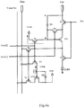
- Figs. 4a-4c are schematic diagrams of current directions and voltage values of the pixel circuit of an embodiment of the present disclosure under different time sequences. In the above respective phases W1-W3, the current directions and the voltage values of the pixel circuit are shown respectively in Fig. 4a , Fig. 4b , and Fig. 4c .
- Scan[2] at this time is at a lowvoltage level, other scan signal lines and the data voltage line are at high voltage levels.
- Fig. 4a in the pixel compensation module 100, only T3 is turned on, now point b is connected to the low voltage level Vcom (for example a grounded line), and the potential of the point b is 0 V, which resets the voltage signal of the last frame in the capacitor C1.
- Vcom for example a grounded line
- T7 is turned on, and T6 and DT2 are turned off, realizing the reset of the touch detection module.
- the potential of the touch electrode d is equal to the voltage applied to the Data line now (for example, Vdata). Since the capacitor C2 is also connected to the touch electrode d, the potential of the touch electrode d is kept to be Vdata.
- Scan[2] is equivalent to the reset scan signal line Reset line of the pixel compensation module 100 and the touch detection module.
- Fig. 5 is a schematic diagram of potential change of the pixel electrode in the pixel circuit provided in the present disclosure.
- the potential Vd of the touch electrode d decreases (for example decrease by Vf), directly causing the gate potential of DT2 to decrease to reach the turning-on condition of DT2.
- Vint inputs an electric singal to Y-read line through DT2 and T6.
- Vd decreases to 0 continuously due to the discharge of the capacitor C2.
- Scan[1] as the scan signal in the X direction also has the collection function (since the signal in the Y direction can be collected only when Scan[1] is at a low voltage level, and Scan[1] in pixels of a specific row is a low voltage level signal at a specific time; as such, it is possible to determine which row Scan[1] has scanned according to the time of the collected touch signal to further determine the coordinates of X). In such a way, the X, Y coordinates of the finger touch position are determined. Such a procedure only needs a finger to perform touch, and the coordinate position can be collected any time.
- Scan[1] functions as the X direction touch signal read line X-read line.
- the touch detection module In the touch detection module, none of the devices operates, and the touch detection module is at a halt state, such as to reduce the impact on the display procedure.
- the present disclosure also provides a display panel comprising the above pixel circuit.
- the pixel circuits are distributed periodically on the display panel.
- one pixel circuit (PU) provided by embodiments of the present disclosure is arranged every three pixels.
- the present disclosure also provides a display apparatus comprising the above display panel.
- the display apparatus here can be any product or means with display function such as an electronic paper, a cell phone, a tablet, a TV set, a display, a notebook computer, a digital photo frame, a navigator and so on.
Abstract
Description
- The present disclosure relates to a pixel circuit, a display panel and a display apparatus.
- With rapid development of display technologies, display apparatuses with touch function are becoming more and more popular due to their advantages such as visualized operation. According to different relative positions of the touch screen panel relative to the display panel, existing display apparatuses with touch function can be generally classified into two categories, the on cell touch screen panel and the in cell touch screen panel. Compared with the on cell touch screen panel, the in cell touch screen panel has smaller thickness and higher light transmittance.
- As for existing display apparatuses, the OLED (Organic Light Emitting Diode) as a current type light emitting device is more and more applied to high performance display areas due to its characteristics such as self light emitting, fast response, wide angle of view and ability of being fabricated on a flexible substrate. According to different driving manners, OLED display apparatuses can be classified into two categories, the PMOLED (Passive Matrix Driving OLED) and the AMOLED (Active Matrix Driving OLED). The AMOLED display is expected to become the next generation new flat display in place of the LCD (Liquid Crystal Display) due to its advantages such as low fabrication cost, high response speed, energy saving, DC driving applicable to portable devices, large operating temperature range. In existing AMOLED display panels, each OLED is driven to emit light by a pixel driving circuit composed of multiple TFTs (Thin Film Transistors) within one pixel unit on the array substrate to realize display. The pixel driving circuit directly determines the quality of the light emitting display of the OLED. Therefore, the design of the pixel driving circuit is key technological content of the AMOLED.
Fig. 1 is a schematic circuit structure diagram of a normal pixel driving circuit. As shown inFig. 1 , the pixel driving circuit comprises a switch TFT T1, a driving TFT T2 and a storage capacitor C, and T1 and T2 here are both P channel driving TFTs. A gate of T1 is connected to a scan line Scan[1], a source of T1 is connected to a data voltage line Data, and a drain of T1 is connected to terminal B of the capacitor C. Terminal A of C is connected to a drain of T2. Terminal B of C is also connected to a gate of T2, a source of T2 is connected to an operating voltage Vdd, and a drain of T2 is connected to a corresponding OLED. When Scan[1] scans to a row of pixel circuit to be a low voltage level, T1 is controlled to turn on, and the data voltage Vdd is written to terminal B of C. When the scan of this row is over, Scan[1] becomes a high voltage level, and T1 is turned off. The data voltage stored in C drives T2 to make it generate current to drive the OLED to ensure that the OLED keeps emitting light within the time of one frame. The saturation current of T2 (i.e., the current following through the OLED) IOLED=K (VGS-Vth)2, where K is a current constant related to T2, VGS is voltage of the gate relative to the source of T2, and Vth is a threshold voltage of T2. It can be seen that IOLED is related to the threshold voltage Vth of T2. In addition, due to fabrication process, device aging and so on, in such a 2T1C pixel driving circuit, the threshold voltage Vth of the driving TFTs at each pixel point would drift, that is, the threshold voltages of the driving TFTs at different pixel points are not uniform, which is easy to make the current flowing through the OLED at each pixel point varies with Vth, such that the display brightness of the display screen is not uniform, influencing the display effect of the whole picture. - On the other hand, the in cell TSP (Touch Screen Panel) fabricates a sensor for touch and a driving circuit in each pixel unit on the array substrate by the array process as well. If the sensor and the driving circuit of TSP are superimposed in an AMOLED pixel unit, it is necessary to add a certain number of driving circuit TFTs. Therefore, certain space of the pixel unit needs to be occupied additionally, but the free space in the pixel unit is limited. This dramatically limits the simultaneous fabrication of the in cell touch screen panel and the AMOLED driving circuit.
- At least one embodiment of the present disclosure provides a pixel circuit and a display apparatus to avoid the influence of a threshold drift of a driving circuit on the display effect and improve the integration level of an in cell touch screen panel circuit and a pixel driving circuit.
- At least one embodiment of the present disclosure provides a pixel circuit comprising a pixel compensation module, a light emitting module and a touch detection module; wherein
the pixel compensation module comprises first to fifth switch units, a pixel driving unit and an energy storage unit;
control terminals of the first switch unit and the fifth switch unit are both connected to a first scan signal line; a first terminal of the first switch unit is connected to an operating voltage, a second terminal of the first switch unit is connected to an input terminal of the pixel driving unit; a first terminal of the fifth switch unit is connected to an output terminal of the pixel driving unit, a second terminal of the fifth switch unit is connected to the light emitting module;
control terminals of the second switch unit and the fourth switch unit are both connected to a second scan signal line; a first terminal of the second switch unit is connected to the input terminal of the pixel driving unit, a second terminal of the second switch unit is connected to a second terminal of the energy storage unit and a control terminal of the pixel driving unit; a first terminal of the fourth switch unit is connected to the output terminal of the pixel driving unit, a second terminal of the fourth switch unit is connected to a data voltage line;
a control terminal of the third switch unit is connected to a third scan signal line, a first terminal of the third switch unit is connected to the second terminal of the energy storage unit, a second terminal of the third switch unit is connected to a low voltage level line;
the touch detection module comprises a detection sub-module and an output sub-module; the detection sub-module is connected to the third scan signal line, a second operating voltage, the data voltage line respectively for detecting a touch signal; the output sub-module is connected to the second scan signal line, a touch signal read line and the detection sub-module respectively for outputting a touch detection signal to the touch signal read line according to an input of the second scan signal line. - Optionally, the light emitting module comprises an electroluminescent element whose anode is connected to the second terminal of the fifth switch unit.
- Optionally, the energy storage unit is a capacitor.
- Optionally, the output sub-module comprises a sixth switch unit whose first terminal is connected to the touch signal read line and whose second terminal is connected to the detection sub-module.
- Optionally, the detection sub-module comprises a seventh unit, a touch signal driving unit, a sensing capacitor and a touch electrode, a first terminal of the seventh switch unit is connected to the data voltage line, a second terminal of the seventh switch unit is connected to a control terminal of the touch signal driving unit, a control terminal of the seventh switch unit is connected to the third scan signal line; an input terminal of the touch signal driving unit is connected to the second operating voltage, an output terminal of the touch signal driving unit is connected to the sixth switch unit; the sensing capacitor is connected between the input terminal and the control terminal of the touch signal driving unit; the touch electrode is connected to the control terminal of the touch signal driving unit.
- Optionally, the respective switch units and driving units are TFTs.
- Optionally, each TFT is of P channel type; the control terminal of the driving unit is a gate of a TFT, the input terminal of the driving unit is a source, the output terminal of the driving unit is a drain; the control terminal of each switch unit is a gate of a TFT, the first terminal and the second terminal of each switch unit correspond to a source and a drain respectively.
- The present disclosure also provides a display panel comprising the above described pixel circuits.
- Further, the pixel circuits are distributed periodically on the display panel.
- The present disclosure also provides a display apparatus comprising the above described display panel.
- In the pixel circuit provided by the present disclosure, a pixel compensation module and a touch detection module are integrated, and the pixel compensation module and the touch detection module share a data voltage line and scan signal lines. As such, it is possible to reduce the number of signal lines, such that the pitch of pixels is dramatically reduced and IC cost is decreased, achieving higher pixel density. At the same time, in the pixel circuit provided by the present disclosure, the operating current flowing through the electroluminescent unit is not influenced by the threshold voltage of the corresponding driving transistor, and it is possible to avoid nonuniformity in brightness of display caused by threshold voltage drift of driving transistors.
-
-
Fig. 1 is a circuit structure diagram of a normal pixel driving circuit; -
Fig. 2 is a schematic circuit structure diagram of a pixel circuit provided by an embodiment of the present disclosure; -
Fig. 3 is a time sequence diagram of key signals in a driving method for a pixel circuit provided by an embodiment of the present disclosure; -
Figs. 4a-4c are schematic diagrams of current directions and voltage values of a pixel circuit provided by an embodiment of the present disclosure under different time sequences; -
Fig. 5 is a schematic diagram of potential change of the pixel electrode in a pixel circuit provided by the present disclosure; -
Fig. 6 is a schematic diagram of positional relation between pixel circuits and pixels in a display panel provided by an embodiment of the present disclosure. - In the following, specific implementations of the present disclosure are further described in connection with figures and embodiments. The following embodiments are only for more clearly illustrating the technical solutions of the present disclosure, but not for limiting the protection scope of the present disclosure. In the figures, the same reference symbols represent the same elements.
-
Fig. 2 is a schematic circuit structure diagram of a pixel circuit provided by an embodiment of the present disclosure. As shown inFig. 2 , the pixel circuit comprises: - a
pixel compensation module 100, alight emitting module 200 and a touch detection module. - The
pixel compensation module 100 comprises a first switch unit T1, a second switch unit T2, a third switch unit T3, a fourth switch unit T4, a fifth switch unit T5, a pixel driving unit DT1, and an energy storage unit C1. A first terminal of the first switch unit T1 is connected to an operating voltage Vdd, a second terminal of the first switch unit T1 is connected to an input terminal of the pixel driving unit DT1, a first terminal of the fifth switch unit T5 is connected to an output terminal of the pixel driving unit DT1, and a second terminal of the fifth switch unit T5 is connected to the light emitting module; control terminals of the first switch unit T1 and the fifth switch unit T5 are both connected to a first scan signal line Em, and a control terminal of the pixel driving unit DT1 is connected to a second terminal b of the energy storage capacitor C1. - A first terminal of the second switch unit T2 is connected to the input terminal of the pixel driving unit DT1, a second terminal of the second switch unit T2 is connected to the second terminal b of the energy storage unit C1, and a control terminal of the second switch unit T2 is connected to a second scan signal line Scan[1].
- A first terminal of the third switch unit T3 is connected to the second terminal b of the energy storage unit C1, a second terminal of the third switch unit T3 is connected to a low voltage level Vcom, a control terminal of the third switch unit T3 is connected to a third scan signal line Scan[2].
- A first terminal of the fourth switch unit T4 is connected to the output terminal of the pixel driving unit DT1, a second terminal of the fourth switch unit T4 is connected to a data voltage line Data, and a control terminal of the fourth switch unit T4 is connected to the second scan signal line Scan[1].
- A first terminal a of the energy storage unit C1 is connected to the operating voltage Vdd.
- The touch detection module comprises a
detection sub-module 310 and anoutput sub-module 320. Thedetection sub-module 310 is connected to the third scan signal line Scan[2], a second operating voltage Vint, and the data voltage line Data respectively for detecting a touch signal; the output sub-module is connected to the second scan signal line Scan[1], a touch signal read line Y-read line and thedetection sub-module 310 respectively for outputting a touch detection signal to the touch signal read line Y-read line according to an input of the second scan signal line Scan[1]. - In the pixel circuit provided in the present disclosure, a pixel compensation module and a touch detection module are integrated, and the pixel compensation module and the touch detection module share a data voltage line and scan signal lines. As such, it is possible to reduce the number of signal lines, such that the pitch of pixels is dramatically reduced and IC cost is decreased, achieving higher pixel density. At the same time, the operating current flowing through the electroluminescent unit is not influenced by the threshold voltage of the corresponding driving transistor, solving the nonuniformity in brightness of display caused by threshold voltage drift of driving transistors.
- Here, the second operating voltage Vint is used to provide driving pulses required to detect a touch.
- For example, the
light emitting module 200 can comprise an electroluminescent element whose anode is connected to the second terminal of T5. - In embodiments of the present disclosure, the electroluminescent element can be various normal devices with electroluminescent function including LED (Light Emitting Diode) or OLED (Organic Light Emitting Diode). In embodiments of the present disclosure, OLED is taken as an example for description.
- Further, the energy storage unit is a capacitor. However, in practical applications, the energy storage unit can adopt other elements with energy storage function.
- Further, as shown in
Fig. 2 , theoutput sub-module 320 comprises a sixth switch unit T6 whose first terminal is connected to the touch signal read line Y-read Line, whose second terminal is connected to thedetection sub-module 310, and whose control terminal is connected to the second scan signal line Scan[1]. - Further, the
detection sub-module 310 comprises a seventh unit T7, a touch signal driving unit DT2, a sensing capacitor C2 and a touch electrode d, a first terminal of the seventh switch unit T7 is connected to the data voltage line Data, a second terminal of the seventh switch unit T7 is connected to a control terminal of the touch signal driving unit DT2, a control terminal of the seventh switch unit is connected to the third scan signal line Scan[2]; an input terminal of the touch signal driving unit DT2 is connected to the second operating voltage Vint, an output terminal of the touch signal driving unit DT2 is connected to the sixth switch unit T6; the sensing capacitor C2 is connected between the input terminal and the control terminal of the touch signal driving unit DT2; the touch electrode d is connected to the control terminal of DT2. Since one terminal of C2 is also connected to the control terminal of DT2, that one terminal of C2 connected to the control terminal of DT2 is also connected to the touch electrode d. - Further, respective switch units and driving units are TFTs.
- Further, as shown in
Fig. 2 , each TFT is of P channel type. Now, the input terminal of the driving unit is a source of a TFT, the output terminal of the driving unit is a drain of the TFT and the control terminal of the driving unit is a gate of the TFT. For each switch unit, the control terminal is also a gate of a TFT, and the first terminal and the second terminal correspond to a source and a drain of the TFT respectively. - It is easy to understand that, the transistors corresponding to the driving units and the switch units here can be transistors whose source and drain can be exchanged, or according to different types of channels, the first terminals of each switch unit and each driving unit can be drains of transistors and the second terminals can be sources of the transistors. The circuit structure obtained by reversing the source and the drain of each transistor in the pixel circuit provided in the present disclosure by those skilled in the art without creative work and able to achieve the same or similar technical effects as those of the technical solutions provided in the present disclosure should also fall in the protection scope of the present disclosure.
- Using the same type of transistors can realize unification of process procedures such as to improve the yield of the products. It can be understood by those skilled in the art that the types of the transistors can be not completely the same in practical applications. For example, T1 and T5 can be N channel transistors, and T4 and T6 can be P channel transistors. As long as two switch units whose control terminals are connected to the same scan signal line can have the same ON/OFF state, the technical solutions provided in the present application can be realized. The implementations described in the present disclosure should not be understood as limiting of the protection scope of the present disclosure.
- Next, the operating principles of the pixel circuit in
Fig. 2 will be described in connection withFig. 3 andFig. 4 . In order to facilitate the description, for example, respective switch units and driving units are P channel TFTs, and the energy storage unit is a capacitor.Fig. 3 is a possible time sequence diagram of scan signals on respective scan signal lines and the data voltage Vdata on the data voltage line within one frame when the pixel circuit provided in the present disclosure operates, which can be divided into three phases that are represented respectively as a first phase W1 (the phase in which the pixel compensation module resets and the touch detection module resets), a second phase W2 (the phase in which the pixel compensation module charges and the touch detection module detects), and a third phase W3 (the phase in which the pixel compensation module emits light and the touch detection module halts) inFig. 3 .Figs. 4a-4c are schematic diagrams of current directions and voltage values of the pixel circuit of an embodiment of the present disclosure under different time sequences. In the above respective phases W1-W3, the current directions and the voltage values of the pixel circuit are shown respectively inFig. 4a ,Fig. 4b , andFig. 4c . - In the first phase W1, referring to
Fig. 3 , Scan[2] at this time is at a lowvoltage level, other scan signal lines and the data voltage line are at high voltage levels. Referring toFig. 4a , in thepixel compensation module 100, only T3 is turned on, now point b is connected to the low voltage level Vcom (for example a grounded line), and the potential of the point b is 0 V, which resets the voltage signal of the last frame in the capacitor C1. - In the touch detection module, T7 is turned on, and T6 and DT2 are turned off, realizing the reset of the touch detection module. After reset, the potential of the touch electrode d is equal to the voltage applied to the Data line now (for example, Vdata). Since the capacitor C2 is also connected to the touch electrode d, the potential of the touch electrode d is kept to be Vdata. As can be seen, Scan[2] is equivalent to the reset scan signal line Reset line of the
pixel compensation module 100 and the touch detection module. - In the second phase W2, referring to
Fig. 3 , now Scan[1] is at a low voltage level, other scan signal lines are at high voltage levels, and the voltage at the Data line remains unchanged. Referring toFig. 4b , in thepixel compensation module 100, T2 and T4 are turned on, and T1, T3 and T5 are turned off. Since point b is grounded before, the pixel driving unit DT1 is turned on, and the Data line charges point b through T4→DT1→T2 until point b is charged to Vdata-Vth (the potential difference between the gate and the source of DT1 is Vth, and Vth is the threshold voltage of DT1). At the same time, since the potential of point a is always Vdd and the potential of point b always remains at Vdata-Vth after the charging is finished, and in addition, since the turning off of T5 makes the current not flow through OLED, the life loss of OLED is indirectly reduced. - In the touch detection module, referring to
Fig. 4b , T7 is turned off, and T6 is turned on.Fig. 5 is a schematic diagram of potential change of the pixel electrode in the pixel circuit provided in the present disclosure. In the second phase W2, as shown inFig. 5 , when a finger touches, referring to the dashed line part of the figure, the potential Vd of the touch electrode d decreases (for example decrease by Vf), directly causing the gate potential of DT2 to decrease to reach the turning-on condition of DT2. Now, Vint inputs an electric singal to Y-read line through DT2 and T6. After the finger touch causes Vd to be directly decreased by Vf, Vd decreases to 0 continuously due to the discharge of the capacitor C2. However, if there is no finger touch at this time, referring to the solid line part, the potential Vd of the touch electrode d will not decrease, but still remain at Vdata. Now, DT2 is turned off, and no electrical signal can be detected in Y-read line. - Only when the gate-source voltage of DT2 satisfies the turning-on condition of the MOS transistor, there is a signal passing through DT2. Such a phase of "waiting" for the gate potential of DT2 to decrease is a buffer phase for the touch signal driving unit, and the main cause of the decrease is the touch of a finger.
- Now, if a finger touches, the potential of the touch electrode d will be directly caused to decrease, and the turning-on condition of DT2 is reached. At this point, the I&V characteristic curve is in the amplification region, DT2 as an amplification TFT will turn on and amplify the signal of coupling pulses, and Y-Read line collects the signal in the Y direction. Scan[1] as the scan signal in the X direction (row direction) also has the collection function (since the signal in the Y direction can be collected only when Scan[1] is at a low voltage level, and Scan[1] in pixels of a specific row is a low voltage level signal at a specific time; as such, it is possible to determine which row Scan[1] has scanned according to the time of the collected touch signal to further determine the coordinates of X). In such a way, the X, Y coordinates of the finger touch position are determined. Such a procedure only needs a finger to perform touch, and the coordinate position can be collected any time.
- It can be seen that, in an embodiment of the present disclosure, Scan[1] functions as the X direction touch signal read line X-read line.
- In the third phase W3, as shown in
Fig. 3 , only Em is at a low voltage level, and other scan signal lines are at high voltage levels. As shown inFig. 4c , in thepixel compensation module 100, now T1 and T5 are turned on, and T2, T3 and T4 are turned off. Vdd makes OLED start to emit light through T1→DT1→T5. - In the touch detection module, none of the devices operates, and the touch detection module is at a halt state, such as to reduce the impact on the display procedure.
- Therefore, according to the current characteristic of TFT in the saturation region, it is possible to obtain the current flowing through the pixel driving unit DT1 as:

- It can be seen from the above equation that the operating current IOLED is no longer affected by Vth, but only related to the difference between Vdd and Vdata, which fully solves the problem of threshold voltage (Vth) drift of the driving TFTs caused by the fabrication process and long time operation, eliminates its influence on IOLED, and ensures normal operation of OLED.
- The present disclosure also provides a display panel comprising the above pixel circuit.
- Optionally, the pixel circuits are distributed periodically on the display panel. In practical applications, it is not necessary for all the positions corresponding to respective pixels to each adopt the pixel circuit provided by embodiments of the present disclosure (for example, among three pixels, one is provided with the pixel circuit provided by embodiments of the present disclosure, and the other pixels are provided with normal pixel circuits) to realize the detection of the touch signal. As shown in
Fig. 6 , one pixel circuit (PU) provided by embodiments of the present disclosure is arranged every three pixels. - The present disclosure also provides a display apparatus comprising the above display panel.
- The display apparatus here can be any product or means with display function such as an electronic paper, a cell phone, a tablet, a TV set, a display, a notebook computer, a digital photo frame, a navigator and so on.
- The above descriptions are only alternative implementations of the present disclosure. It should be noted that those skilled in the art can make various variations and improvements without departing from the technical principle of the present disclosure. These variations and improvements are also intended to be incorporated within the protection scope of the present disclosure.
- The present application claims the priority of Chinese Patent Application No.
201410302129.8 filed on June 27, 2014
Claims (10)
- A pixel circuit comprising a pixel compensation module, a light emitting module and a touch detection module; wherein
the pixel compensation module comprises first to fifth switch units, a pixel driving unit and an energy storage unit;
control terminals of the first switch unit and the fifth switch unit are both connected to a first scan signal line, a first terminal of the first switch unit is connected to an operating voltage, a second terminal of the first switch unit is connected to an input terminal of the pixel driving unit, a first terminal of the fifth switch unit is connected to an output terminal of the pixel driving unit, a second terminal of the fifth switch unit is connected to the light emitting module;
control terminals of the second switch unit and the fourth switch unit are both connected to a second scan signal line, a first terminal of the second switch unit is connected to the input terminal of the pixel driving unit, a second terminal of the second switch unit is connected to a second terminal of the energy storage unit and a control terminal of the pixel driving unit, a first terminal of the fourth switch unit is connected to the output terminal of the pixel driving unit, a second terminal of the fourth switch unit is connected to a data voltage line;
a control terminal of the third switch unit is connected to a third scan signal line, a first terminal of the third switch unit is connected to the second terminal of the energy storage unit, a second terminal of the third switch unit is connected to a low voltage level line;
the touch detection module comprises a detection sub-module and an output sub-module, the detection sub-module is connected to the third scan signal line, a second operating voltage, the data voltage line respectively for detecting a touch signal, the output sub-module is connected to the second scan signal line, a touch signal read line and the detection sub-module respectively for outputting a touch detection signal to the touch signal read line according to the input of the second scan signal line. - The pixel circuit according to claim 1, wherein the light emitting module comprises an electroluminescent element whose anode is connected to the second terminal of the fifth switch unit.
- The pixel circuit according to claim 1 or 2, wherein the energy storage unit is a capacitor.
- The pixel circuit according to any one of claims I to 3, wherein the output sub-module comprises a sixth switch unit whose first terminal is connected to the touch signal read line and whose second terminal is connected to the detection sub-module.
- The pixel circuit according to any one of claims 1 to 4, wherein the detection sub-module comprises a seventh unit, a touch signal driving unit, a sensing capacitor and a touch electrode, a first terminal of the seventh switch unit is connected to the data voltage line, a second terminal of the seventh switch unit is connected to a control terminal of the touch signal driving unit, a control terminal of the seventh switch unit is connected to the third scan signal line; an input terminal of the touch signal driving unit is connected to the second operating voltage, an output terminal of the touch signal driving unit is connected to the sixth switch unit; the sensing capacitor is connected between the input terminal and the control terminal of the touch signal driving unit; the touch electrode is connected to the control terminal of the touch signal driving unit.
- The pixel circuit according to any one of claims 1 to 5, wherein the respective switch units and driving units are TFTs.
- The pixel circuit according to claim 6, wherein each TFT is of P channel type; the control terminal of the driving units is a gate of a TFT, the input terminal of the driving unit is a source, the output terminal of the driving unit is a drain; the control terminal of each switch unit is a gate of a TFT, the first terminal and the second terminal of each switch unit are correspond to a source and a drain respectively.
- A display panel comprising pixel circuits according to any one of claims 1 to 7.
- The display panel according to claim 8, wherein the pixel circuits are distributed periodically on the display panel.
- A display apparatus comprising a display panel according to claim 8 or 9.
Applications Claiming Priority (2)
| Application Number | Priority Date | Filing Date | Title |
|---|---|---|---|
| CN201410302129.8A CN104091562B (en) | 2014-06-27 | 2014-06-27 | Image element circuit, display panel and display device |
| PCT/CN2014/087052 WO2015196598A1 (en) | 2014-06-27 | 2014-09-22 | Pixel circuit, display panel and display device |
Publications (3)
| Publication Number | Publication Date |
|---|---|
| EP3163559A1 true EP3163559A1 (en) | 2017-05-03 |
| EP3163559A4 EP3163559A4 (en) | 2017-11-08 |
| EP3163559B1 EP3163559B1 (en) | 2019-02-20 |
Family
ID=51639273
Family Applications (1)
| Application Number | Title | Priority Date | Filing Date |
|---|---|---|---|
| EP14859320.5A Active EP3163559B1 (en) | 2014-06-27 | 2014-09-22 | Pixel circuit, display panel and display device |
Country Status (3)
| Country | Link |
|---|---|
| EP (1) | EP3163559B1 (en) |
| CN (1) | CN104091562B (en) |
| WO (1) | WO2015196598A1 (en) |
Cited By (2)
| Publication number | Priority date | Publication date | Assignee | Title |
|---|---|---|---|---|
| EP3557565A1 (en) * | 2018-04-19 | 2019-10-23 | InnoLux Corporation | Display device and manufacturing method of display substrate |
| US11367389B2 (en) | 2017-11-29 | 2022-06-21 | Chengdu Boe Optoelectronics Technology Co., Ltd. | Pixel circuit and method for driving the same, display panel and display apparatus |
Families Citing this family (14)
| Publication number | Priority date | Publication date | Assignee | Title |
|---|---|---|---|---|
| CN104282263A (en) * | 2014-09-25 | 2015-01-14 | 京东方科技集团股份有限公司 | Pixel circuit, drive method thereof, display panel and display device |
| KR102172389B1 (en) | 2014-12-30 | 2020-10-30 | 엘지디스플레이 주식회사 | Organic light emitting display |
| CN104778917B (en) * | 2015-01-30 | 2017-12-19 | 京东方科技集团股份有限公司 | Pixel-driving circuit and its driving method and display device |
| CN104575398B (en) * | 2015-02-10 | 2017-04-05 | 京东方科技集团股份有限公司 | Image element circuit and its driving method, display device |
| CN107705748B (en) * | 2015-10-30 | 2023-10-27 | 京东方科技集团股份有限公司 | Display substrate, driving method thereof and display device |
| CN105590955A (en) * | 2015-12-25 | 2016-05-18 | 昆山国显光电有限公司 | Pixel circuit and driving method thereof, and active matrix organic light emitting display |
| CN106448554A (en) * | 2016-11-30 | 2017-02-22 | 武汉华星光电技术有限公司 | OLED (organic light-emitting diode) driving circuit and OLED display panel |
| CN108399890B (en) * | 2018-05-30 | 2020-08-18 | 上海天马有机发光显示技术有限公司 | Organic light-emitting display panel, driving method thereof and organic light-emitting display device |
| CN109830179B (en) * | 2019-03-29 | 2021-01-08 | 维沃移动通信有限公司 | Terminal equipment and photosensitive detection method for terminal equipment |
| CN109979367B (en) * | 2019-05-13 | 2023-08-04 | 京东方科技集团股份有限公司 | Photoelectric detection circuit, driving method thereof, photosensitive device and display device |
| CN110534046B (en) * | 2019-08-30 | 2023-03-10 | 京东方科技集团股份有限公司 | Array substrate, display device and data compensation method |
| CN114694573A (en) * | 2020-12-28 | 2022-07-01 | 上海和辉光电股份有限公司 | Pixel driving circuit and display device |
| CN114035020A (en) * | 2021-09-29 | 2022-02-11 | 重庆康佳光电技术研究院有限公司 | Back board circuit detection device and method |
| CN117354640A (en) * | 2023-10-12 | 2024-01-05 | 之江实验室 | Antagonistic pixel circuit, driving method of antagonistic pixel circuit, and detector |
Family Cites Families (9)
| Publication number | Priority date | Publication date | Assignee | Title |
|---|---|---|---|---|
| JP4747552B2 (en) * | 2004-10-19 | 2011-08-17 | セイコーエプソン株式会社 | Electro-optical device, electronic apparatus and method |
| JP4857586B2 (en) * | 2005-04-05 | 2012-01-18 | セイコーエプソン株式会社 | Electronic circuit driving method and driving circuit, light emitting device, and electronic apparatus |
| KR101279115B1 (en) * | 2006-06-27 | 2013-06-26 | 엘지디스플레이 주식회사 | Pixel Circuit of Organic Light Emitting Display |
| JP2009271200A (en) * | 2008-05-01 | 2009-11-19 | Sony Corp | Display apparatus and driving method for display apparatus |
| CN103208255B (en) * | 2013-04-15 | 2015-05-20 | 京东方科技集团股份有限公司 | Pixel circuit, driving method for driving the pixel circuit and display device |
| CN203179480U (en) * | 2013-04-26 | 2013-09-04 | 北京京东方光电科技有限公司 | Pixel unit control circuit and display device |
| CN203192370U (en) * | 2013-04-28 | 2013-09-11 | 京东方科技集团股份有限公司 | Pixel circuit and display device |
| CN103383837B (en) * | 2013-07-09 | 2015-07-01 | 京东方科技集团股份有限公司 | Touch and display drive circuit, drive method and display device |
| CN203941677U (en) * | 2014-06-27 | 2014-11-12 | 京东方科技集团股份有限公司 | Image element circuit, display panel and display device |
-
2014
- 2014-06-27 CN CN201410302129.8A patent/CN104091562B/en active Active
- 2014-09-22 WO PCT/CN2014/087052 patent/WO2015196598A1/en active Application Filing
- 2014-09-22 EP EP14859320.5A patent/EP3163559B1/en active Active
Cited By (3)
| Publication number | Priority date | Publication date | Assignee | Title |
|---|---|---|---|---|
| US11367389B2 (en) | 2017-11-29 | 2022-06-21 | Chengdu Boe Optoelectronics Technology Co., Ltd. | Pixel circuit and method for driving the same, display panel and display apparatus |
| EP3557565A1 (en) * | 2018-04-19 | 2019-10-23 | InnoLux Corporation | Display device and manufacturing method of display substrate |
| US10930196B2 (en) | 2018-04-19 | 2021-02-23 | Innolux Corporation | Display device and manufacturing method of display substrate |
Also Published As
| Publication number | Publication date |
|---|---|
| CN104091562B (en) | 2016-01-13 |
| EP3163559A4 (en) | 2017-11-08 |
| EP3163559B1 (en) | 2019-02-20 |
| CN104091562A (en) | 2014-10-08 |
| WO2015196598A1 (en) | 2015-12-30 |
Similar Documents
| Publication | Publication Date | Title |
|---|---|---|
| EP3163559B1 (en) | Pixel circuit, display panel and display device | |
| EP3163562B1 (en) | Pixel circuit, display panel and display device | |
| EP3154050B1 (en) | Pixel circuit and display device | |
| US9778800B2 (en) | Pixel circuit, display panel and display apparatus | |
| EP3159882B1 (en) | Pixel circuit, driving method therefor and display device | |
| US10068950B2 (en) | Pixel circuit, driving method thereof, and display apparatus | |
| EP3163561B1 (en) | Pixel circuit and drive method therefor, organic light-emitting display panel and display device | |
| US10545607B2 (en) | Pixel circuit and driving method, display panel and display apparatus | |
| EP3151228B1 (en) | Pixel circuit and display device | |
| US20170243537A1 (en) | Pixel circuit and driving method thereof, and display device | |
| EP3159879B1 (en) | Pixel circuit and display device | |
| US20150049046A1 (en) | Amoled Pixel Circuit, a Driving Method Thereof and a Display Device | |
| EP3159878A1 (en) | Pixel circuit and display device | |
| EP3719786B1 (en) | Pixel circuit and drive method thereof, and display panel and display apparatus | |
| CN203941676U (en) | Image element circuit, display panel and display device | |
| CN203941677U (en) | Image element circuit, display panel and display device | |
| US9430969B2 (en) | Driving circuit and driving method for AMOLED pixel circuit |
Legal Events
| Date | Code | Title | Description |
|---|---|---|---|
| PUAI | Public reference made under article 153(3) epc to a published international application that has entered the european phase |
Free format text: ORIGINAL CODE: 0009012 |
|
| STAA | Information on the status of an ep patent application or granted ep patent |
Free format text: STATUS: REQUEST FOR EXAMINATION WAS MADE |
|
| 17P | Request for examination filed |
Effective date: 20150512 |
|
| AK | Designated contracting states |
Kind code of ref document: A1 Designated state(s): AL AT BE BG CH CY CZ DE DK EE ES FI FR GB GR HR HU IE IS IT LI LT LU LV MC MK MT NL NO PL PT RO RS SE SI SK SM TR |
|
| AX | Request for extension of the european patent |
Extension state: BA ME |
|
| DAX | Request for extension of the european patent (deleted) | ||
| A4 | Supplementary search report drawn up and despatched |
Effective date: 20171010 |
|
| RIC1 | Information provided on ipc code assigned before grant |
Ipc: G09G 3/3233 20160101ALI20171004BHEP Ipc: G09G 3/32 20160101AFI20171004BHEP |
|
| GRAP | Despatch of communication of intention to grant a patent |
Free format text: ORIGINAL CODE: EPIDOSNIGR1 |
|
| STAA | Information on the status of an ep patent application or granted ep patent |
Free format text: STATUS: GRANT OF PATENT IS INTENDED |
|
| INTG | Intention to grant announced |
Effective date: 20180903 |
|
| GRAS | Grant fee paid |
Free format text: ORIGINAL CODE: EPIDOSNIGR3 |
|
| GRAA | (expected) grant |
Free format text: ORIGINAL CODE: 0009210 |
|
| STAA | Information on the status of an ep patent application or granted ep patent |
Free format text: STATUS: THE PATENT HAS BEEN GRANTED |
|
| AK | Designated contracting states |
Kind code of ref document: B1 Designated state(s): AL AT BE BG CH CY CZ DE DK EE ES FI FR GB GR HR HU IE IS IT LI LT LU LV MC MK MT NL NO PL PT RO RS SE SI SK SM TR |
|
| REG | Reference to a national code |
Ref country code: GB Ref legal event code: FG4D |
|
| REG | Reference to a national code |
Ref country code: CH Ref legal event code: EP |
|
| REG | Reference to a national code |
Ref country code: DE Ref legal event code: R096 Ref document number: 602014041516 Country of ref document: DE |
|
| REG | Reference to a national code |
Ref country code: AT Ref legal event code: REF Ref document number: 1099234 Country of ref document: AT Kind code of ref document: T Effective date: 20190315 |
|
| REG | Reference to a national code |
Ref country code: IE Ref legal event code: FG4D |
|
| REG | Reference to a national code |
Ref country code: NL Ref legal event code: FP |
|
| REG | Reference to a national code |
Ref country code: LT Ref legal event code: MG4D |
|
| PG25 | Lapsed in a contracting state [announced via postgrant information from national office to epo] |
Ref country code: LT Free format text: LAPSE BECAUSE OF FAILURE TO SUBMIT A TRANSLATION OF THE DESCRIPTION OR TO PAY THE FEE WITHIN THE PRESCRIBED TIME-LIMIT Effective date: 20190220 Ref country code: PT Free format text: LAPSE BECAUSE OF FAILURE TO SUBMIT A TRANSLATION OF THE DESCRIPTION OR TO PAY THE FEE WITHIN THE PRESCRIBED TIME-LIMIT Effective date: 20190620 Ref country code: NO Free format text: LAPSE BECAUSE OF FAILURE TO SUBMIT A TRANSLATION OF THE DESCRIPTION OR TO PAY THE FEE WITHIN THE PRESCRIBED TIME-LIMIT Effective date: 20190520 Ref country code: FI Free format text: LAPSE BECAUSE OF FAILURE TO SUBMIT A TRANSLATION OF THE DESCRIPTION OR TO PAY THE FEE WITHIN THE PRESCRIBED TIME-LIMIT Effective date: 20190220 Ref country code: SE Free format text: LAPSE BECAUSE OF FAILURE TO SUBMIT A TRANSLATION OF THE DESCRIPTION OR TO PAY THE FEE WITHIN THE PRESCRIBED TIME-LIMIT Effective date: 20190220 |
|
| PG25 | Lapsed in a contracting state [announced via postgrant information from national office to epo] |
Ref country code: HR Free format text: LAPSE BECAUSE OF FAILURE TO SUBMIT A TRANSLATION OF THE DESCRIPTION OR TO PAY THE FEE WITHIN THE PRESCRIBED TIME-LIMIT Effective date: 20190220 Ref country code: RS Free format text: LAPSE BECAUSE OF FAILURE TO SUBMIT A TRANSLATION OF THE DESCRIPTION OR TO PAY THE FEE WITHIN THE PRESCRIBED TIME-LIMIT Effective date: 20190220 Ref country code: BG Free format text: LAPSE BECAUSE OF FAILURE TO SUBMIT A TRANSLATION OF THE DESCRIPTION OR TO PAY THE FEE WITHIN THE PRESCRIBED TIME-LIMIT Effective date: 20190520 Ref country code: GR Free format text: LAPSE BECAUSE OF FAILURE TO SUBMIT A TRANSLATION OF THE DESCRIPTION OR TO PAY THE FEE WITHIN THE PRESCRIBED TIME-LIMIT Effective date: 20190521 Ref country code: IS Free format text: LAPSE BECAUSE OF FAILURE TO SUBMIT A TRANSLATION OF THE DESCRIPTION OR TO PAY THE FEE WITHIN THE PRESCRIBED TIME-LIMIT Effective date: 20190620 Ref country code: LV Free format text: LAPSE BECAUSE OF FAILURE TO SUBMIT A TRANSLATION OF THE DESCRIPTION OR TO PAY THE FEE WITHIN THE PRESCRIBED TIME-LIMIT Effective date: 20190220 |
|
| REG | Reference to a national code |
Ref country code: AT Ref legal event code: MK05 Ref document number: 1099234 Country of ref document: AT Kind code of ref document: T Effective date: 20190220 |
|
| PG25 | Lapsed in a contracting state [announced via postgrant information from national office to epo] |
Ref country code: AL Free format text: LAPSE BECAUSE OF FAILURE TO SUBMIT A TRANSLATION OF THE DESCRIPTION OR TO PAY THE FEE WITHIN THE PRESCRIBED TIME-LIMIT Effective date: 20190220 Ref country code: ES Free format text: LAPSE BECAUSE OF FAILURE TO SUBMIT A TRANSLATION OF THE DESCRIPTION OR TO PAY THE FEE WITHIN THE PRESCRIBED TIME-LIMIT Effective date: 20190220 Ref country code: IT Free format text: LAPSE BECAUSE OF FAILURE TO SUBMIT A TRANSLATION OF THE DESCRIPTION OR TO PAY THE FEE WITHIN THE PRESCRIBED TIME-LIMIT Effective date: 20190220 Ref country code: DK Free format text: LAPSE BECAUSE OF FAILURE TO SUBMIT A TRANSLATION OF THE DESCRIPTION OR TO PAY THE FEE WITHIN THE PRESCRIBED TIME-LIMIT Effective date: 20190220 Ref country code: EE Free format text: LAPSE BECAUSE OF FAILURE TO SUBMIT A TRANSLATION OF THE DESCRIPTION OR TO PAY THE FEE WITHIN THE PRESCRIBED TIME-LIMIT Effective date: 20190220 Ref country code: RO Free format text: LAPSE BECAUSE OF FAILURE TO SUBMIT A TRANSLATION OF THE DESCRIPTION OR TO PAY THE FEE WITHIN THE PRESCRIBED TIME-LIMIT Effective date: 20190220 Ref country code: SK Free format text: LAPSE BECAUSE OF FAILURE TO SUBMIT A TRANSLATION OF THE DESCRIPTION OR TO PAY THE FEE WITHIN THE PRESCRIBED TIME-LIMIT Effective date: 20190220 Ref country code: CZ Free format text: LAPSE BECAUSE OF FAILURE TO SUBMIT A TRANSLATION OF THE DESCRIPTION OR TO PAY THE FEE WITHIN THE PRESCRIBED TIME-LIMIT Effective date: 20190220 |
|
| REG | Reference to a national code |
Ref country code: DE Ref legal event code: R097 Ref document number: 602014041516 Country of ref document: DE |
|
| PG25 | Lapsed in a contracting state [announced via postgrant information from national office to epo] |
Ref country code: SM Free format text: LAPSE BECAUSE OF FAILURE TO SUBMIT A TRANSLATION OF THE DESCRIPTION OR TO PAY THE FEE WITHIN THE PRESCRIBED TIME-LIMIT Effective date: 20190220 Ref country code: PL Free format text: LAPSE BECAUSE OF FAILURE TO SUBMIT A TRANSLATION OF THE DESCRIPTION OR TO PAY THE FEE WITHIN THE PRESCRIBED TIME-LIMIT Effective date: 20190220 |
|
| PLBE | No opposition filed within time limit |
Free format text: ORIGINAL CODE: 0009261 |
|
| STAA | Information on the status of an ep patent application or granted ep patent |
Free format text: STATUS: NO OPPOSITION FILED WITHIN TIME LIMIT |
|
| PG25 | Lapsed in a contracting state [announced via postgrant information from national office to epo] |
Ref country code: AT Free format text: LAPSE BECAUSE OF FAILURE TO SUBMIT A TRANSLATION OF THE DESCRIPTION OR TO PAY THE FEE WITHIN THE PRESCRIBED TIME-LIMIT Effective date: 20190220 |
|
| 26N | No opposition filed |
Effective date: 20191121 |
|
| PG25 | Lapsed in a contracting state [announced via postgrant information from national office to epo] |
Ref country code: SI Free format text: LAPSE BECAUSE OF FAILURE TO SUBMIT A TRANSLATION OF THE DESCRIPTION OR TO PAY THE FEE WITHIN THE PRESCRIBED TIME-LIMIT Effective date: 20190220 |
|
| PG25 | Lapsed in a contracting state [announced via postgrant information from national office to epo] |
Ref country code: TR Free format text: LAPSE BECAUSE OF FAILURE TO SUBMIT A TRANSLATION OF THE DESCRIPTION OR TO PAY THE FEE WITHIN THE PRESCRIBED TIME-LIMIT Effective date: 20190220 |
|
| PG25 | Lapsed in a contracting state [announced via postgrant information from national office to epo] |
Ref country code: MC Free format text: LAPSE BECAUSE OF FAILURE TO SUBMIT A TRANSLATION OF THE DESCRIPTION OR TO PAY THE FEE WITHIN THE PRESCRIBED TIME-LIMIT Effective date: 20190220 |
|
| REG | Reference to a national code |
Ref country code: CH Ref legal event code: PL |
|
| PG25 | Lapsed in a contracting state [announced via postgrant information from national office to epo] |
Ref country code: CH Free format text: LAPSE BECAUSE OF NON-PAYMENT OF DUE FEES Effective date: 20190930 Ref country code: LU Free format text: LAPSE BECAUSE OF NON-PAYMENT OF DUE FEES Effective date: 20190922 Ref country code: IE Free format text: LAPSE BECAUSE OF NON-PAYMENT OF DUE FEES Effective date: 20190922 Ref country code: LI Free format text: LAPSE BECAUSE OF NON-PAYMENT OF DUE FEES Effective date: 20190930 |
|
| REG | Reference to a national code |
Ref country code: BE Ref legal event code: MM Effective date: 20190930 |
|
| PG25 | Lapsed in a contracting state [announced via postgrant information from national office to epo] |
Ref country code: BE Free format text: LAPSE BECAUSE OF NON-PAYMENT OF DUE FEES Effective date: 20190930 |
|
| PG25 | Lapsed in a contracting state [announced via postgrant information from national office to epo] |
Ref country code: CY Free format text: LAPSE BECAUSE OF FAILURE TO SUBMIT A TRANSLATION OF THE DESCRIPTION OR TO PAY THE FEE WITHIN THE PRESCRIBED TIME-LIMIT Effective date: 20190220 |
|
| PG25 | Lapsed in a contracting state [announced via postgrant information from national office to epo] |
Ref country code: HU Free format text: LAPSE BECAUSE OF FAILURE TO SUBMIT A TRANSLATION OF THE DESCRIPTION OR TO PAY THE FEE WITHIN THE PRESCRIBED TIME-LIMIT; INVALID AB INITIO Effective date: 20140922 Ref country code: MT Free format text: LAPSE BECAUSE OF FAILURE TO SUBMIT A TRANSLATION OF THE DESCRIPTION OR TO PAY THE FEE WITHIN THE PRESCRIBED TIME-LIMIT Effective date: 20190220 |
|
| PG25 | Lapsed in a contracting state [announced via postgrant information from national office to epo] |
Ref country code: MK Free format text: LAPSE BECAUSE OF FAILURE TO SUBMIT A TRANSLATION OF THE DESCRIPTION OR TO PAY THE FEE WITHIN THE PRESCRIBED TIME-LIMIT Effective date: 20190220 |
|
| PGFP | Annual fee paid to national office [announced via postgrant information from national office to epo] |
Ref country code: NL Payment date: 20230920 Year of fee payment: 10 Ref country code: GB Payment date: 20230823 Year of fee payment: 10 |
|
| PGFP | Annual fee paid to national office [announced via postgrant information from national office to epo] |
Ref country code: FR Payment date: 20230822 Year of fee payment: 10 Ref country code: DE Payment date: 20230919 Year of fee payment: 10 |