EP3160130A1 - Processing device, image pickup device, and endoscope system - Google Patents
Processing device, image pickup device, and endoscope system Download PDFInfo
- Publication number
- EP3160130A1 EP3160130A1 EP15809065.4A EP15809065A EP3160130A1 EP 3160130 A1 EP3160130 A1 EP 3160130A1 EP 15809065 A EP15809065 A EP 15809065A EP 3160130 A1 EP3160130 A1 EP 3160130A1
- Authority
- EP
- European Patent Office
- Prior art keywords
- pixel signal
- illumination
- pulsed light
- signal
- light
- Prior art date
- Legal status (The legal status is an assumption and is not a legal conclusion. Google has not performed a legal analysis and makes no representation as to the accuracy of the status listed.)
- Withdrawn
Links
- 238000005286 illumination Methods 0.000 claims abstract description 411
- 238000006243 chemical reaction Methods 0.000 claims abstract description 8
- 238000003384 imaging method Methods 0.000 claims description 74
- 239000011159 matrix material Substances 0.000 claims description 13
- 210000001260 vocal cord Anatomy 0.000 claims description 8
- 238000000034 method Methods 0.000 abstract description 17
- 238000010586 diagram Methods 0.000 description 34
- 238000003780 insertion Methods 0.000 description 14
- 230000037431 insertion Effects 0.000 description 14
- 230000002194 synthesizing effect Effects 0.000 description 9
- 238000005452 bending Methods 0.000 description 7
- 230000003287 optical effect Effects 0.000 description 7
- 238000005096 rolling process Methods 0.000 description 5
- 230000000694 effects Effects 0.000 description 3
- 239000000835 fiber Substances 0.000 description 3
- 238000001727 in vivo Methods 0.000 description 3
- 230000001360 synchronised effect Effects 0.000 description 3
- 238000005401 electroluminescence Methods 0.000 description 2
- XLYOFNOQVPJJNP-UHFFFAOYSA-N water Substances O XLYOFNOQVPJJNP-UHFFFAOYSA-N 0.000 description 2
- NAWXUBYGYWOOIX-SFHVURJKSA-N (2s)-2-[[4-[2-(2,4-diaminoquinazolin-6-yl)ethyl]benzoyl]amino]-4-methylidenepentanedioic acid Chemical compound C1=CC2=NC(N)=NC(N)=C2C=C1CCC1=CC=C(C(=O)N[C@@H](CC(=C)C(O)=O)C(O)=O)C=C1 NAWXUBYGYWOOIX-SFHVURJKSA-N 0.000 description 1
- 230000005540 biological transmission Effects 0.000 description 1
- 238000001574 biopsy Methods 0.000 description 1
- 239000003990 capacitor Substances 0.000 description 1
- 230000000295 complement effect Effects 0.000 description 1
- 230000020169 heat generation Effects 0.000 description 1
- 239000004973 liquid crystal related substance Substances 0.000 description 1
- 229910044991 metal oxide Inorganic materials 0.000 description 1
- 150000004706 metal oxides Chemical class 0.000 description 1
- 230000002093 peripheral effect Effects 0.000 description 1
- 239000004065 semiconductor Substances 0.000 description 1
Images







Classifications
-
- A—HUMAN NECESSITIES
- A61—MEDICAL OR VETERINARY SCIENCE; HYGIENE
- A61B—DIAGNOSIS; SURGERY; IDENTIFICATION
- A61B1/00—Instruments for performing medical examinations of the interior of cavities or tubes of the body by visual or photographical inspection, e.g. endoscopes; Illuminating arrangements therefor
- A61B1/06—Instruments for performing medical examinations of the interior of cavities or tubes of the body by visual or photographical inspection, e.g. endoscopes; Illuminating arrangements therefor with illuminating arrangements
- A61B1/0655—Control therefor
-
- A—HUMAN NECESSITIES
- A61—MEDICAL OR VETERINARY SCIENCE; HYGIENE
- A61B—DIAGNOSIS; SURGERY; IDENTIFICATION
- A61B1/00—Instruments for performing medical examinations of the interior of cavities or tubes of the body by visual or photographical inspection, e.g. endoscopes; Illuminating arrangements therefor
- A61B1/00002—Operational features of endoscopes
- A61B1/00004—Operational features of endoscopes characterised by electronic signal processing
- A61B1/00009—Operational features of endoscopes characterised by electronic signal processing of image signals during a use of endoscope
-
- A—HUMAN NECESSITIES
- A61—MEDICAL OR VETERINARY SCIENCE; HYGIENE
- A61B—DIAGNOSIS; SURGERY; IDENTIFICATION
- A61B1/00—Instruments for performing medical examinations of the interior of cavities or tubes of the body by visual or photographical inspection, e.g. endoscopes; Illuminating arrangements therefor
- A61B1/00002—Operational features of endoscopes
- A61B1/00043—Operational features of endoscopes provided with output arrangements
- A61B1/00045—Display arrangement
-
- A—HUMAN NECESSITIES
- A61—MEDICAL OR VETERINARY SCIENCE; HYGIENE
- A61B—DIAGNOSIS; SURGERY; IDENTIFICATION
- A61B1/00—Instruments for performing medical examinations of the interior of cavities or tubes of the body by visual or photographical inspection, e.g. endoscopes; Illuminating arrangements therefor
- A61B1/00064—Constructional details of the endoscope body
- A61B1/00071—Insertion part of the endoscope body
- A61B1/0008—Insertion part of the endoscope body characterised by distal tip features
- A61B1/00096—Optical elements
-
- A—HUMAN NECESSITIES
- A61—MEDICAL OR VETERINARY SCIENCE; HYGIENE
- A61B—DIAGNOSIS; SURGERY; IDENTIFICATION
- A61B1/00—Instruments for performing medical examinations of the interior of cavities or tubes of the body by visual or photographical inspection, e.g. endoscopes; Illuminating arrangements therefor
- A61B1/04—Instruments for performing medical examinations of the interior of cavities or tubes of the body by visual or photographical inspection, e.g. endoscopes; Illuminating arrangements therefor combined with photographic or television appliances
- A61B1/045—Control thereof
-
- A—HUMAN NECESSITIES
- A61—MEDICAL OR VETERINARY SCIENCE; HYGIENE
- A61B—DIAGNOSIS; SURGERY; IDENTIFICATION
- A61B1/00—Instruments for performing medical examinations of the interior of cavities or tubes of the body by visual or photographical inspection, e.g. endoscopes; Illuminating arrangements therefor
- A61B1/04—Instruments for performing medical examinations of the interior of cavities or tubes of the body by visual or photographical inspection, e.g. endoscopes; Illuminating arrangements therefor combined with photographic or television appliances
- A61B1/05—Instruments for performing medical examinations of the interior of cavities or tubes of the body by visual or photographical inspection, e.g. endoscopes; Illuminating arrangements therefor combined with photographic or television appliances characterised by the image sensor, e.g. camera, being in the distal end portion
-
- A—HUMAN NECESSITIES
- A61—MEDICAL OR VETERINARY SCIENCE; HYGIENE
- A61B—DIAGNOSIS; SURGERY; IDENTIFICATION
- A61B1/00—Instruments for performing medical examinations of the interior of cavities or tubes of the body by visual or photographical inspection, e.g. endoscopes; Illuminating arrangements therefor
- A61B1/267—Instruments for performing medical examinations of the interior of cavities or tubes of the body by visual or photographical inspection, e.g. endoscopes; Illuminating arrangements therefor for the respiratory tract, e.g. laryngoscopes, bronchoscopes
- A61B1/2673—Instruments for performing medical examinations of the interior of cavities or tubes of the body by visual or photographical inspection, e.g. endoscopes; Illuminating arrangements therefor for the respiratory tract, e.g. laryngoscopes, bronchoscopes for monitoring movements of vocal chords
-
- G—PHYSICS
- G02—OPTICS
- G02B—OPTICAL ELEMENTS, SYSTEMS OR APPARATUS
- G02B23/00—Telescopes, e.g. binoculars; Periscopes; Instruments for viewing the inside of hollow bodies; Viewfinders; Optical aiming or sighting devices
- G02B23/24—Instruments or systems for viewing the inside of hollow bodies, e.g. fibrescopes
- G02B23/2407—Optical details
- G02B23/2446—Optical details of the image relay
-
- G—PHYSICS
- G02—OPTICS
- G02B—OPTICAL ELEMENTS, SYSTEMS OR APPARATUS
- G02B23/00—Telescopes, e.g. binoculars; Periscopes; Instruments for viewing the inside of hollow bodies; Viewfinders; Optical aiming or sighting devices
- G02B23/24—Instruments or systems for viewing the inside of hollow bodies, e.g. fibrescopes
- G02B23/2407—Optical details
- G02B23/2461—Illumination
- G02B23/2469—Illumination using optical fibres
-
- G—PHYSICS
- G02—OPTICS
- G02B—OPTICAL ELEMENTS, SYSTEMS OR APPARATUS
- G02B23/00—Telescopes, e.g. binoculars; Periscopes; Instruments for viewing the inside of hollow bodies; Viewfinders; Optical aiming or sighting devices
- G02B23/24—Instruments or systems for viewing the inside of hollow bodies, e.g. fibrescopes
- G02B23/2476—Non-optical details, e.g. housings, mountings, supports
- G02B23/2484—Arrangements in relation to a camera or imaging device
-
- G—PHYSICS
- G03—PHOTOGRAPHY; CINEMATOGRAPHY; ANALOGOUS TECHNIQUES USING WAVES OTHER THAN OPTICAL WAVES; ELECTROGRAPHY; HOLOGRAPHY
- G03B—APPARATUS OR ARRANGEMENTS FOR TAKING PHOTOGRAPHS OR FOR PROJECTING OR VIEWING THEM; APPARATUS OR ARRANGEMENTS EMPLOYING ANALOGOUS TECHNIQUES USING WAVES OTHER THAN OPTICAL WAVES; ACCESSORIES THEREFOR
- G03B7/00—Control of exposure by setting shutters, diaphragms or filters, separately or conjointly
- G03B7/08—Control effected solely on the basis of the response, to the intensity of the light received by the camera, of a built-in light-sensitive device
- G03B7/091—Digital circuits
- G03B7/093—Digital circuits for control of exposure time
-
- H—ELECTRICITY
- H04—ELECTRIC COMMUNICATION TECHNIQUE
- H04N—PICTORIAL COMMUNICATION, e.g. TELEVISION
- H04N23/00—Cameras or camera modules comprising electronic image sensors; Control thereof
- H04N23/56—Cameras or camera modules comprising electronic image sensors; Control thereof provided with illuminating means
-
- H—ELECTRICITY
- H04—ELECTRIC COMMUNICATION TECHNIQUE
- H04N—PICTORIAL COMMUNICATION, e.g. TELEVISION
- H04N23/00—Cameras or camera modules comprising electronic image sensors; Control thereof
- H04N23/70—Circuitry for compensating brightness variation in the scene
- H04N23/73—Circuitry for compensating brightness variation in the scene by influencing the exposure time
-
- H—ELECTRICITY
- H04—ELECTRIC COMMUNICATION TECHNIQUE
- H04N—PICTORIAL COMMUNICATION, e.g. TELEVISION
- H04N23/00—Cameras or camera modules comprising electronic image sensors; Control thereof
- H04N23/70—Circuitry for compensating brightness variation in the scene
- H04N23/74—Circuitry for compensating brightness variation in the scene by influencing the scene brightness using illuminating means
-
- H—ELECTRICITY
- H04—ELECTRIC COMMUNICATION TECHNIQUE
- H04N—PICTORIAL COMMUNICATION, e.g. TELEVISION
- H04N23/00—Cameras or camera modules comprising electronic image sensors; Control thereof
- H04N23/70—Circuitry for compensating brightness variation in the scene
- H04N23/745—Detection of flicker frequency or suppression of flicker wherein the flicker is caused by illumination, e.g. due to fluorescent tube illumination or pulsed LED illumination
-
- H—ELECTRICITY
- H04—ELECTRIC COMMUNICATION TECHNIQUE
- H04N—PICTORIAL COMMUNICATION, e.g. TELEVISION
- H04N23/00—Cameras or camera modules comprising electronic image sensors; Control thereof
- H04N23/70—Circuitry for compensating brightness variation in the scene
- H04N23/76—Circuitry for compensating brightness variation in the scene by influencing the image signals
-
- H—ELECTRICITY
- H04—ELECTRIC COMMUNICATION TECHNIQUE
- H04N—PICTORIAL COMMUNICATION, e.g. TELEVISION
- H04N23/00—Cameras or camera modules comprising electronic image sensors; Control thereof
- H04N23/95—Computational photography systems, e.g. light-field imaging systems
-
- H—ELECTRICITY
- H04—ELECTRIC COMMUNICATION TECHNIQUE
- H04N—PICTORIAL COMMUNICATION, e.g. TELEVISION
- H04N25/00—Circuitry of solid-state image sensors [SSIS]; Control thereof
- H04N25/70—SSIS architectures; Circuits associated therewith
- H04N25/71—Charge-coupled device [CCD] sensors; Charge-transfer registers specially adapted for CCD sensors
-
- H—ELECTRICITY
- H04—ELECTRIC COMMUNICATION TECHNIQUE
- H04N—PICTORIAL COMMUNICATION, e.g. TELEVISION
- H04N25/00—Circuitry of solid-state image sensors [SSIS]; Control thereof
- H04N25/70—SSIS architectures; Circuits associated therewith
- H04N25/76—Addressed sensors, e.g. MOS or CMOS sensors
-
- H—ELECTRICITY
- H04—ELECTRIC COMMUNICATION TECHNIQUE
- H04N—PICTORIAL COMMUNICATION, e.g. TELEVISION
- H04N23/00—Cameras or camera modules comprising electronic image sensors; Control thereof
- H04N23/50—Constructional details
- H04N23/555—Constructional details for picking-up images in sites, inaccessible due to their dimensions or hazardous conditions, e.g. endoscopes or borescopes
-
- H—ELECTRICITY
- H04—ELECTRIC COMMUNICATION TECHNIQUE
- H04N—PICTORIAL COMMUNICATION, e.g. TELEVISION
- H04N25/00—Circuitry of solid-state image sensors [SSIS]; Control thereof
- H04N25/50—Control of the SSIS exposure
- H04N25/53—Control of the integration time
- H04N25/531—Control of the integration time by controlling rolling shutters in CMOS SSIS
Definitions
- the present invention relates to a processing device for processing a pixel signal, an imaging device, and an endoscope system.
- an endoscope system is used to observe the inside of a subject.
- the endoscope system captures an in-vivo image by inserting a flexible insertion unit having an elongated shape into the subject such as a patient, intermittently emitting illumination light from the distal end of the insertion unit, and receiving reflected light of the illumination light by using an imaging unit at a distal end portion of the insertion unit.
- the in-vivo image captured in this way is displayed on a display of the endoscope system.
- CMOS Complementary Metal Oxide Semiconductor
- a technique that generates a display image by removing areas having luminance greater than or equal to a predetermined threshold value from a frame image (for example, see Patent Literature 1).
- a technique is also proposed that can secure a certain level of luminance in the entire area of an image by causing a light source to emit illumination light in a period common to all pixels in an exposure period of each pixel of an image sensor (for example, see Patent Literature 2).
- illumination timing and read timing are asynchronous, so that even when an enough period to be able to commonly expose all the pixels is secured, there is a case in which the illumination timing overlaps with the read timing. In this case, an exposure amount varies between images and brightness variation between images cannot be eliminated, and thus, image quality may not be maintained.
- the present invention has been made in view of the foregoing, and an object of the present invention is to provide a processing device, an imaging device, and an endoscope system that can maintain image quality even if pulsed light is emitted at any timing with respect to the read timing of the image sensor.
- a processing device processes a pixel signal of a plurality of pixels configured to receive light from a subject illuminated with pulsed light and to perform photoelectric conversion on the received light to generate the pixel signal.
- the processing device includes a signal processing unit configured to generate, from the pixel signal, an illumination time pixel signal that is a pixel signal generated when the plurality of pixels is exposed in an illumination period of the pulsed light, according to an overlapping state between the illumination period of the pulsed light and read timing of the pixel signal.
- the processing device further includes a storage unit configured to store the pixel signal for each frame in accordance with a matrix arrangement of the plurality of pixels.
- the signal processing unit is configured to generate the illumination time pixel signal corresponding to the illumination period of the pulsed light for each frame for each illumination period of the pulsed light from the pixel signal of a plurality of continuous frames stored in the storage unit.
- the processing device further includes a detecting unit configured to acquire the read timing and the illumination period of the pulsed light and detects a pixel row in which the read timing overlaps with the illumination period of the pulsed light, in which the illumination time pixel signal is generated, from the pixel signal as an overlap pixel row.
- the signal processing unit is configured to generate an illumination time pixel signal of the overlap pixel row based on a pixel signal of the overlap pixel row read at an overlap timing that overlaps with the illumination period of the pulsed light and a pixel signal of the overlap pixel row in the pixel signal of a frame that is read after the overlap timing.
- the signal processing unit is configured to generate the illumination time pixel signal based on a pixel signal of the non-overlap pixel row in the pixel signal of a frame that is read after the illumination period of the pulsed light in which the illumination time pixel signal is generated.
- the processing device further includes a display controller configured to generate a display image signal to be displayed by a display device from an illumination time pixel signal of a plurality of frames generated by the signal processing unit in accordance with a display cycle of the display device connected to the processing device.
- An imaging device includes: a light receiving unit having a plurality of pixels arranged in a matrix form, the plurality of pixels being configured to receive light from a subject illuminated with pulsed light and to perform photoelectric conversion on the received light to generate a pixel signal; a reading unit configured to perform exposure on the plurality of pixels of the light receiving unit and to read the pixel signal from the plurality of pixels of the light receiving unit; and a signal processing unit configured to generate, from the pixel signal read by the reading unit, an illumination time pixel signal that is a pixel signal generated when the plurality of pixels is exposed in an illumination period of the pulsed light, according to an overlapping state between the illumination period of the pulsed light and read timing of the pixel signal read by the reading unit.
- the imaging device further includes a storage unit configured to store the pixel signal for each frame in accordance with a matrix arrangement of the plurality of pixels in the light receiving unit.
- the signal processing unit is configured to generate the illumination time pixel signal corresponding to the illumination period of the pulsed light for each frame for each illumination period of the pulsed light from the pixel signal of a plurality of continuous frames stored in the storage unit.
- the imaging device further includes a detecting unit configured to acquire the read timing and the illumination period of the pulsed light and detects a pixel row in which the read timing overlaps with the illumination period of the pulsed light, in which the illumination time pixel signal is generated, from the pixel signal as an overlap pixel row.
- the signal processing unit is configured to generate an illumination time pixel signal of the overlap pixel row based on a pixel signal of the overlap pixel row read at an overlap timing that overlaps with the illumination period of the pulsed light and a pixel signal of the overlap pixel row in the pixel signal of a frame that is read after the overlap timing.
- the signal processing unit is configured to generate the illumination time pixel signal based on a pixel signal of the non-overlap pixel row in the pixel signal of a frame that is read after the illumination period of the pulsed light in which the illumination time pixel signal is generated.
- the imaging device further includes a display controller configured to generate a display image signal to be displayed by a display device from an illumination time pixel signal of a plurality of frames generated by the signal processing unit in accordance with a display cycle of the display device connected to the imaging device.
- the light receiving unit and the reading unit are constituted by a CMOS image sensor.
- the light receiving unit and the reading unit are constituted by a CCD image sensor.
- An endoscope system includes: a light source configured to emit pulsed light to illuminate a subject; a light receiving unit having a plurality of pixels arranged in a matrix form, the plurality of pixels being configured to receive light from the subject illuminated with the pulsed light emitted from the light source and to perform photoelectric conversion on the received light to generate a pixel signal; a reading unit configured to perform exposure on the plurality of pixels of the light receiving unit and to read the pixel signal from the plurality of pixels of the light receiving unit; and a signal processing unit configured to generate, from the pixel signal read by the reading unit, an illumination time pixel signal that is a pixel signal generated when the plurality of pixels is exposed in an illumination period of the pulsed light, according to an overlapping state between the illumination period of the pulsed light emitted from the light source and read timing of the pixel signal read by the reading unit.
- the endoscope system further includes a storage unit configured to store the pixel signal for each frame in accordance with a matrix arrangement of the plurality of pixels in the light receiving unit.
- the signal processing unit is configured to generate the illumination time pixel signal corresponding to the illumination period of the pulsed light for each frame for each illumination period of the pulsed light from the pixel signal of a plurality of continuous frames stored in the storage unit.
- the endoscope system further includes a detecting unit configured to acquire the read timing and the illumination period of the pulsed light and detects a pixel row in which the read timing overlaps with the illumination period of the pulsed light, in which the illumination time pixel signal is generated, from the pixel signal as an overlap pixel row.
- the signal processing unit is configured to generate an illumination time pixel signal of the overlap pixel row based on a pixel signal of the overlap pixel row read at an overlap timing that overlaps with the illumination period of the pulsed light and a pixel signal of the overlap pixel row in the pixel signal of a frame that is read after the overlap timing.
- the signal processing unit is configured to generate the illumination time pixel signal based on a pixel signal of the non-overlap pixel row in the pixel signal of a frame that is read after the illumination period of the pulsed light in which the illumination time pixel signal is generated.
- the endoscope system further includes a display controller configured to generate a display image signal to be displayed by a display device from an illumination time pixel signal of a plurality of frames generated by the signal processing unit in accordance with a display cycle of the display device connected to the endoscope system.
- the subject is vocal cords.
- the endoscope system further includes: a voice input unit to which a voice is configured to be input; a vibration cycle detecting unit configured to detect a vibration cycle of the voice input into the voice input unit; and a light source controller configured to control an illumination timing and the illumination period of the pulsed light from the light source in synchronization with the vibration cycle of the voice detected by the vibration cycle detecting unit.
- the endoscope system further includes a light source controller configured to: synchronize an illumination timing of the pulsed light from the light source with a frame cycle of the light receiving unit and the reading unit; and control the illumination period of the pulsed light from the light source based on the pixel signal read by the reading unit.
- the light receiving unit and the reading unit are constituted by a CMOS image sensor.
- the light receiving unit and the reading unit are constituted by a CCD image sensor.
- an illumination time pixel signal is generated from a pixel signal of a plurality of pixels that has received light from a subject irradiated with pulsed light, according to an overlapping state between illumination timing of the pulsed light and read timing of the pixel signal.
- the illumination time pixel signal is a pixel signal generated when the plurality of pixels is exposed in an illumination period of the pulsed light.
- FIG. 1 is a schematic diagram illustrating a schematic configuration of an endoscope system according to a first embodiment of the present invention.
- the endoscope system 1 includes an endoscope 2 (scope) which is introduced into a subject and captures an image inside the subject to generate an image signal of inside of the subject, a voice input device 3 to which a voice is input, a light source device 5 that generates pulsed light as illumination light (observation light) of the endoscope 2, a processing device 4 which performs predetermined image processing on the image signal captured by the endoscope 2 and controls each element of the endoscope system 1, and a display device 6 which displays an image corresponding to the image signal on which the processing device 4 performs the image processing.
- an endoscope 2 (scope) which is introduced into a subject and captures an image inside the subject to generate an image signal of inside of the subject
- a voice input device 3 to which a voice is input
- a light source device 5 that generates pulsed light as illumination light (observation light) of the endoscope 2
- the endoscope 2 includes an insertion unit 21 that is inserted into the subject, an operating unit 22 which is provided at a proximal end portion of the insertion unit 21 and held by an operator, and a flexible universal cord 23 that extends from the operating unit 22.
- the insertion unit 21 is realized by using an illumination fiber (light guide cable), an electric cable, and the like.
- the insertion unit 21 includes a distal end portion 211 including an imaging unit incorporating a CMOS image sensor as an image sensor that captures an image inside the subject, a bendable bending portion 212 formed by a plurality of bending pieces, and a flexible tube portion 213 having flexibility provided at the proximal end portion of the bending portion 212.
- the distal end portion 211 is provided with an illumination unit that illuminates inside the subject through an illumination lens, an observation unit that captures an image inside the subject, an opening portion 214 through which a processing tool channel passes, and an air/water nozzle (not illustrated in FIG. 1 ).
- the operating unit 22 includes a bending knob 221 that bends the bending portion 212 in a vertical direction and a horizontal direction, a treatment tool insertion portion 222 through which treatment tools such as biopsy forceps and a laser scalpel are inserted into a body cavity of the subject, and a plurality of switch units 223 for operating peripheral apparatuses such as the processing device 4, the light source device 5, an air supply device, a water supply device, and a gas supply device.
- a treatment tool inserted from the treatment tool insertion portion 222 is exposed from the opening portion 214 at the distal end of the insertion unit 21 through a treatment tool channel provided inside the insertion unit 21.
- the universal cord 23 is formed by using an illumination fiber, an electric cable, and the like.
- the universal cord 23 is split at its proximal end.
- An end portion of one branch cord 231 is a connector 232 and the proximal end of the other branch cord 234 is a connector 233.
- the connector 232 is attachable to and detachable from the processing device 4.
- the connector 233 is attachable to and detachable from the light source device 5.
- the universal cord 23 transmits an image signal captured by the imaging unit provided in the distal end portion 211 to the processing device 4 through the connector 232.
- the universal cord 23 propagates the illumination light emitted from the light source device 5 to the distal end portion 211 through the connector 233, the operating unit 22, and the flexible tube portion 213.
- the voice input device 3 is input with a voice issued from vocal cords when the subject is the vocal cords.
- a distal end of a cord 31 is connected to the voice input device 3 and a connector 311 at the proximal end of the cord 31 is attachable to and detachable from the processing device 4.
- the voice input device 3 outputs the input voice to the processing device 4 through the cord 31 and the connector 311.
- the processing device 4 performs predetermined image processing on an imaging signal in the subject which is captured by the imaging unit at the distal end portion 211 of the endoscope 2 and input through the universal cord 23.
- the processing device 4 controls each element of the endoscope system 1 based on various instruction signals transmitted from the switch units 223 in the operating unit 22 of the endoscope 2 through the universal cord 23.
- the light source device 5 is formed by using a light source that emits pulse-shaped white light, a condenser lens, and the like.
- the light source device 5 supplies pulse-shaped white light from a white light source to the endoscope 2 connected through the connector 232 and the illumination fiber of the universal cord 23 as illumination light for illuminating inside of the subject which is a subject.
- a part of the pulsed light emitted from the light source device 5 is split at the connector 233 and formed into a pulse signal, and thereafter input into the processing device 4 through the branch cords 234 and 231 and the connector 232.
- the display device 6 is formed by using a display using a liquid crystal or an organic EL (Electro Luminescence).
- the display device 6 displays various information including an image corresponding to a display image signal on which predetermined image processing is performed by the processing device 4 through an image cable 61. Thereby, an operator can observe a desired position in the subject and determine characteristics of the position by operating the endoscope 2 while seeing the image (in-vivo image) displayed by the display device 6.
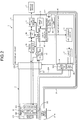
- FIG. 2 is a block diagram schematically illustrating the configuration of the endoscope system 1.
- the endoscope 2 includes an imaging unit 24 at the distal end portion 211.
- the imaging unit 24 includes an optical system 241 such as an objective lens arranged on a light receiving surface side of a light receiving unit 242 described below, the light receiving unit 242 that generates a pixel signal representing the inside of the subject from an optical image formed on the light receiving surface, and a reading unit 243.
- the light receiving unit 242 has a plurality of pixels arranged on the light receiving surface.
- the plurality of pixels is configured to receive light from the subject illuminated with the pulsed light from the light source device 5 and to perform photoelectric conversion on the received light to generate a pixel signal.
- a plurality of pixels is arranged in a matrix form on the light receiving unit 242.
- a plurality of pixel rows horizontal lines
- the light receiving unit 242 generates a pixel signal representing the inside of the subject from the optical image formed on the light receiving surface.
- the reading unit 243 performs exposure on the plurality of pixels in the light receiving unit 242 and reading of the pixel signal from the plurality of pixels.
- the light receiving unit 242 and the reading unit 243 are constituted by, for example, a CMOS image sensor and can perform exposure and reading for each horizontal line.
- the reading unit 243 performs an imaging operation, which performs exposure and reading, from a first horizontal line and generates a pixel signal by a rolling shutter method that performs charge reset, exposure, and reading by shifting timing for each horizontal line. Therefore, in the imaging unit 24, even in one imaging period (frame), the exposure timing and the read timing vary for each horizontal line.
- the reading unit 243 outputs the pixel signal read from the plurality of pixels of the light receiving unit 242 to the processing device 4 through a cable (not illustrated in the drawings) and the connector 232.
- a vertical synchronizing signal and a horizontal synchronizing signal attached to the pixel signal output from the CMOS image sensor are also input into a timing detecting unit 44 described later.
- the processing device 4 includes an input unit 41, a vibrational frequency detecting unit 42, a control unit 43, a timing detecting unit 44, an image processing unit 45 (signal processing unit), a memory 46, and a display controller 47.
- the input unit 41 is realized by using operation devices such as a mouse, a keyboard, and a touch panel and receives input of various instruction information of the endoscope system 1. Specifically, the input unit 41 receives subject information (for example, ID, date of birth, and name), identification information (for example, ID and examination corresponding items) of the endoscope 2, and various instruction information such as examination content.
- subject information for example, ID, date of birth, and name
- identification information for example, ID and examination corresponding items
- various instruction information such as examination content.
- the vibrational frequency detecting unit 42 detects the frequency of a voice which is input into the voice input device 3 and input into the processing device 4 through the cord 31 and the connector 311. The voice is issued from vocal cords which are the subject. The vibrational frequency detecting unit 42 outputs the detected frequency of the voice to the control unit 43.
- the control unit 43 is realized by using a CPU and the like.
- the control unit 43 controls a processing operation of each element of the processing device 4.
- the control unit 43 controls operation of the processing device 4 by transmitting instruction information and data to each element of the processing device 4.
- the control unit 43 is connected to the imaging unit 24 and the light source device 5 through each cable.
- the control unit 43 includes a light source controller 431 that controls operation of the light source device 5.
- the light source controller 431 controls an illumination timing and an illumination period of the pulsed light from a light source 51 in synchronization with the frequency of the voice detected by the vibrational frequency detecting unit 42.
- the control unit 43 also controls operation of the imaging unit 24.
- the timing detecting unit 44 detects the illumination timing and the illumination period of the pulsed light based on a pulse signal which is input from the light source device 5 and which corresponds to the pulsed light from the light source device 5.
- the timing detecting unit 44 detects the read timing of the pixel signal read by the reading unit 243 for each horizontal line based on the vertical synchronizing signal and the horizontal synchronizing signal attached to the pixel signal output from the imaging unit 24.
- the timing detecting unit 44 acquires the read timing, the illumination timing, and the illumination period and detects a horizontal line, where the read timing overlaps with an illumination period in which an illumination time pixel signal described later is generated, as an overlap line from among the pixel signals read by the reading unit 243.
- the image processing unit 45 performs predetermined image processing on the pixel signal of a plurality of pixels read by the reading unit 243 of the imaging unit 24.
- the image processing unit 45 performs image processing including at least optical black subtraction processing, white balance (WB) adjustment processing, image signal synchronization processing when the image sensor is a Bayer array, color matrix calculating processing, gamma correction processing, color reproduction processing, and edge enhancement processing on the pixel signal.
- WB white balance
- the image processing unit 45 generates the illumination time pixel signal which is a pixel signal in a case in which a plurality of pixels is exposed in the illumination period of the pulsed light from the light source device 5 from the pixel signal of a plurality of pixels read by the reading unit 243 of the imaging unit 24 according to an overlapping state between the illumination timing and the illumination period of the pulsed light of the light source device 5 and the read timing of the pixel signal read by the reading unit 243.
- the image processing unit 45 generates the illumination time pixel signal corresponding to the illumination period of illumination for each frame for each illumination timing from pixel signals of a plurality of continuous frames stored in the memory 46 described later.
- the image processing unit 45 For the overlap line, the image processing unit 45 generates the illumination time pixel signal based on a pixel signal of the overlap line read at an overlap timing that overlaps with the illumination period of the pulsed light and a pixel signal of an overlap line in a pixel signal of a frame that is read first after the overlap timing.
- the image processing unit 45 For a non-overlap line which is a horizontal line other than the overlap line, the image processing unit 45 generates the illumination time pixel signal based on a pixel signal of a non-overlap pixel line in a pixel signal of a frame that is read first after the illumination period of the pulsed light in which the illumination time pixel signal is generated.
- the memory 46 is realized by using volatile memory and/or non-volatile memory and stores various programs to operate the processing device 4 and the light source device 5.
- the memory 46 temporarily records information that is being processed by the processing device 4.
- the memory 46 stores the pixel signal read by the reading unit 243 for each frame in accordance with a matrix arrangement of a plurality of pixels in the light receiving unit 242.
- the memory 46 stores the illumination time pixel signal generated by the image processing unit 45 for each frame.
- the memory 46 may be formed by using a memory card or the like attached from the outside of the processing device 4.
- the display controller 47 generates display image data to be displayed by the display device 6 from the illumination time pixel signals of a plurality of frames generated by the image processing unit 45 in accordance with a display cycle of the display device 6.
- the display controller 47 selects display image data from among the illumination time pixel signals of a plurality of frames generated by the image processing unit 45 for each display cycle of the display device 6.
- the display controller 47 generates a display image signal by synthesizing the illumination time pixel signals of a plurality of frames generated by the image processing unit 45 for each display cycle of the display device 6.
- the display controller 47 converts the display image data from a digital signal to an analog signal, changes image data of the converted analog signal into a high-definition television format or the like, and then outputs the image data to the display device 6.
- the light source device 5 includes the light source 51 and a light source driver 52.
- the light source 51 is formed by using a light source such as a white LED that emits pulse-shaped white light and an optical system such as a condenser lens.
- the light source 51 generates the illumination light to be supplied to the endoscope 2.
- the light source driver 52 supplies a predetermined electric power to the light source 51 under control of the light source controller 431. Thereby, the light generated from the light source 51 is emitted to the subject from an illumination window 211a of the distal end portion 211 of the insertion unit 21 through the connector 233 and the universal cord 23.
- the imaging unit 24 is arranged near the illumination window 211a.
- the connector 233 includes a splitter 53 for splitting a part of the pulsed light generated from the light source 51 and inputs the split light into a light detector 54 and the light detector 54 that converts the pulsed light input from the splitter 53 into a pulse signal.
- the splitter 53 is formed by an optical system such as a prism.
- the light detector 54 inputs the converted pulse signal into the timing detecting unit 44 of the processing device 4 through the branch cords 234 and 231 and the connector 232.
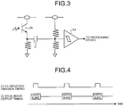
- FIG. 3 is a diagram illustrating an example of a configuration of an electric circuit constituting the light detector 54. As illustrated in FIG. 3 , when the pulsed light enters into the light detector 54, a phototransistor Pt becomes an ON state and an electric current is input into an amplifier Ad through a capacitor C. Thereafter, a DC component is removed from the electric current and the electric current is amplified by the amplifier Ad, so that a pulse signal corresponding to the pulsed light is input into the processing device 4.
- FIG. 4 is a timing chart illustrating an ideal image output timing in the imaging unit 24 with respect to the illumination timing of the pulsed light.
- FIG. 4 when each illumination timing of pulsed light (see FIG. 4 (1)) corresponds with each exposure timing in the imaging unit 24 (see FIG. 4 (2)), variation of brightness does not occur between a plurality of images to be output.
- the illumination timing of the pulsed light of the light source 51 is controlled so as to be synchronized with the vibration frequency of a voice issued from vocal cords which are the subject, so that the illumination timing of the pulsed light does not necessarily correspond with the exposure timing in the imaging unit 24.
- a light emitting cycle of the pulsed light is longer than a frame cycle of the imaging unit 24 and a display cycle in the display device 6.
- the illumination timing of the pulsed light by the light source 51 and the exposure timing and the read timing of the reading unit 243 will be described.
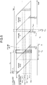
- FIG. 5 is a diagram for explaining the illumination timing of the pulsed light by the light source 51 and the pixel exposure timing and the pixel signal read timing of the reading unit 243.
- (1) of FIG. 5 is a diagram illustrating an example of a timing chart illustrating the illumination timing of the pulsed light emitted from the light source 51.
- (2) of FIG. 5 is a diagram illustrating an example of a timing chart for explaining the exposure timing and the read timing for a plurality of pixels by the reading unit 243. Each pulsed light is output with the same pulse width (illumination period).
- the illumination timing of pulsed light L emitted from the light source 51 is controlled so as to be synchronized with the vibration frequency of a voice issued from vocal cords which are the subject.
- the pulsed light L is emitted from the light source 51 for each cycle Cp illustrated in (1) of FIG. 5 during a period T L .
- the reading unit 243 performs exposure in a period A j and reads the pixel signal at a time R j .
- the pixel signal D (N - 1) of the frame (N - 1) illustrated in FIG. 5 is generated when the exposure on each horizontal line from the first line 1 to the last line j is sequentially performed and the pixel signals of the horizontal lines V are read in order from the first line in a period from the time R 1 to the time R j as illustrated by an arrow Y (N - 1) .
- the rolling shutter method is employed in this way, even in the same frame, the exposure period is temporally shifted between the horizontal lines, so that if the light emitting cycle of the pulsed light from the light source 51 does not correspond with the frame cycle of the imaging unit 24, a plurality of frames may be exposed with one time illumination of the pulsed light.
- the number of times of illumination and the illumination period vary between frames and brightness variation occurs for each horizontal line between frames.
- the light emitting cycle of the pulsed light is longer than the frame cycle of the imaging unit 24, so that the illumination period T L6 of the pulsed light L 6 overlaps with the exposure period of the first half horizontal lines in the frame (N - 1) and the exposure period of the second half horizontal lines in the frame (N - 2).
- an upper area (horizontal lines 1 to s) where all the pulsed light L 6 is exposed is bright
- a central area (horizontal lines (s + 1) to t) where only a part of the pulsed light L 6 is exposed gradually becomes dark
- the next area (horizontal lines (t + 1) to u) where no pulsed light is exposed becomes pitch-dark
- the illumination period T L11 is almost included in the exposure period of the frame N. Therefore, although the pixel signal D N of the frame N becomes a little dark in upper and lower partial areas, the pixel signal D N of the frame N becomes bright in the other area.
- the pixel signal of each frame where the brightness varies due to differences of the number of times of illumination and the illumination period between frames even in the same horizontal lines is not output without change, but the image processing unit 45 of the processing device 4 generates the illumination time pixel signal, which is a pixel signal generated when all the pixels of the light receiving unit 242 are exposed at the illumination timing of the pulsed light, from pixel signals of a plurality of frames, so that a pixel signal where the brightness variation is removed is output.
- generation processing of the illumination time pixel signal in the processing device 4 will be described using an example in which an illumination time pixel signal corresponding to a pixel signal in a case in which all the pixels of the light receiving unit 242 are exposed with the pulsed light L 6 of FIG. 5 (1) is generated.
- the timing detecting unit 44 detects the illumination timing and the illumination period of the pulsed light from the light source 51 and the read timing of each horizontal line of the light receiving unit 242 by the reading unit 243, and detects a horizontal line, where the read timing overlaps with an illumination period in which the illumination time pixel signal is generated, as an overlap line from among the pixel signals read by the reading unit 243. Further, the timing detecting unit 44 detects a horizontal line, where the read timing does not overlap with the illumination period in which the illumination time pixel signal is generated, as a non-overlap line from among the pixel signals read by the reading unit 243.
- the timing detecting unit 44 detects the first horizontal line 1 to the horizontal line s as non-overlap lines where the illumination period T L6 of the pulsed light L 6 does not overlap with the read timing of both the pixel signal D (N-2) of the frame (N - 2) and the pixel signal D (N - 1) of the frame (N - 1).
- the timing detecting unit 44 detects the horizontal line (s + 1) to the horizontal line t as overlap lines where the illumination period T L6 of the pulsed light L 6 overlaps with the read timing of the pixel signal D (N - 2) of the frame (N - 2).
- the timing detecting unit 44 detects the horizontal line (t + 1) to the horizontal line j as non-overlap lines where the illumination period T L6 of the pulsed light L 6 does not overlap with the read timing of any frame.
- the horizontal line m (1 ⁇ m ⁇ s) will be described as an example.
- the entire illumination period T L6 of the pulsed light L 6 in which the illumination time pixel signal is generated, is included in the exposure period of the horizontal line m of the frame (N - 1).
- no pulsed light other than the pulsed light L 6 is emitted in the exposure period of the frame (N - 1).
- each pixel signal of the horizontal lines (t + 1) to j of the frame (N - 2) read after the illumination of the pulsed light L 6 is a pixel signal in a case in which all the pixels located in the horizontal lines (t + 1) to j at the illumination timing of the pulsed light L 6 are exposed.
- the image processing unit 45 applies data of each pixel of each horizontal line of the pixel signal D (N-2) of the frame (N - 2) without change as the illumination time pixel signal of the pulsed light L 6 of the horizontal lines (t +1) to j.
- the image processing unit 45 generates the illumination time pixel signal based on a pixel signal of a non-overlap pixel row of a frame that is read at read timing immediately after the illumination timing of the pulsed light, where the illumination time pixel signal is generated.
- the illumination period T L6 of the pulsed light L 6 overlaps with the read timing of the horizontal line n in the frame (N - 2) and overlaps with both the exposure period of the horizontal line n of the frame (N - 2) and the exposure period of the horizontal line n of the frame (N - 1).
- the other pulsed light is not irradiated neither in the exposure period of the horizontal line n of the frame (N - 2) nor the exposure period of the horizontal line n of the frame (N - 1).
- An output value of a pixel signal by pixels is proportional to a light receiving time in which light is actually received, so that the pixel signal (illumination time pixel signal) generated when the pixels in the horizontal line n are exposed in the illumination period of the pulsed light L 6 is a signal formed by directly synthesizing the pixel signal of the horizontal line n in the pixel signal D (N - 2) of the frame (N - 2) and the pixel signal of the horizontal line n in the pixel signal D (N - 1) of the frame (N - 1). Therefore, the image processing unit 45 calculates the illumination time pixel signal by using the formula (2) below for each pixel x of the horizontal line n.
- Pixel x of n ⁇ th line exposed with pulsed light L 6 Pixel x of n ⁇ th line exposed with pulsed light L 6 of D N ⁇ 2 + Pixel x of n ⁇ th line exposed with pulsed light L 6 of D N ⁇ 1
- the image processing unit 45 For a horizontal line to be an overlap line, the image processing unit 45 generates the illumination time pixel signal of an overlap pixel row by synthesizing a pixel signal of the overlap line that is read at an overlap timing that overlaps with the illumination period and a pixel signal of an overlap line in a pixel signal of a frame immediately after the overlap timing.
- the image processing unit 45 calculates the illumination time pixel signal by using the formula (1) or the formula (2) according to whether a pixel is located in an overlap line or a non-overlap line for each pixel, and outputs the calculated illumination time pixel signal as an image signal for each frame.
- the illumination time pixel signal which is a pixel signal generated when a plurality of pixels is exposed in the illumination period of the pulsed light, is generated from a pixel signal that is read from a plurality of pixels according to the overlapping state between the illumination timing and the illumination period of the pulsed light by the light source 51 and the read timing of the pixel signal, so that even when the pulsed light is emitted at any timing with respect to the read timing of the image sensor, it is possible to eliminate variation of brightness between images to be output and maintain the image quality.
- an algorism is employed in which a frame buffer using DDR3 with a large capacity is used as the memory 46, and when the image processing unit 45 performs calculation, pixel signals of a plurality of frames are processed in one frame period and an illumination time pixel signal of a plurality of frames is generated by performing pipeline processing in a state in which past pixel signals of a plurality of frames are read.
- (1) of FIG. 6 is a timing chart illustrating the vertical synchronizing signal in the CMOS image sensor included in the imaging unit 24, an exposure state of the CMOS image sensor, and data reading.
- (2) of FIG. 6 is a timing chart of data to be detected by the timing detecting unit 44.
- FIG. 6 is a timing chart of a pixel signal for each frame, which is stored in areas 1 to 4 of the memory 46.
- (4) of FIG. 6 is a timing chart of image processing in the image processing unit 45.
- (5) of FIG. 6 is a timing chart of display image data generation processing in the display controller 47.
- the timing detecting unit 44 processes pixel signals of five frames in one frame period. In the current frame period, the timing detecting unit 44 detects the read timings of a pixel signal from five frames ago to one frame ago and the illumination timings and the illumination periods from five frames ago to one frame ago. As illustrated in (3) of FIG. 6 , in each area 1 to 4 of the memory 46, a pixel signal of one frame is stored, and a pixel signal to be stored is newly rewritten for each frame period.
- the image processing unit 45 reads a pixel signal Dg1 of four frames from four frames ago to one frame ago, which are stored in the areas 1 to 4 of the memory 46, generates an illumination time pixel signal, and outputs the generated illumination time pixel signal for each frame (illumination time pixel signals G 6 and G 11 ).
- the generation processing of the illumination time pixel signals G 6 and G 11 in the image processing unit 45 is the same as that described in the description with reference to FIG. 5 .
- the number of frames of the illumination time pixel signal G generated at one time in the image processing unit 45 is not limited to a constant number of frames, but varies according to the number of times of emission of the pulsed light with respect to the frame cycle.
- the display controller 47 generates display image signals M 1 to M 7 to be displayed by the display device 6 from the illumination time pixel signal generated by the image processing unit 45 in accordance with the display cycle of the display device 6.
- the display controller 47 generates the display image signal M 7 from the illumination time pixel signals G 6 and G 11 generated by the image processing unit 45 as illustrated by an arrow Y2 for a display cycle corresponding to the current frame period.
- the generation processing of the display image signal by the display controller 47 will be described with reference to FIGS. 7 and 8 .
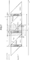
- FIGS. 7 and 8 are diagrams for explaining the generation processing of the display image signal by the display controller 47.
- (1) of FIG. 7 and ( 1 ) of FIG. 8 are timing charts illustrating the display cycle of the display device 6.
- (2) of FIG. 7 and ( 2 ) of FIG. 8 are an example of a timing chart illustrating the illustration timing of the pulsed light emitted from the light source 51.
- (3) of FIG. 7 and ( 3 ) of FIG. 8 are an example of a timing chart for explaining the exposure timing and the read timing of the reading unit 243.
- the time axis of the illumination timing of the pulsed light corresponding to each illumination time pixel signal is moved to and overlapped on the time axis corresponding to the display cycle.
- FIG. 7 and 8 for the purpose of explanation, the time axis of the illumination timing of the pulsed light corresponding to each illumination time pixel signal is moved to and overlapped on the time axis corresponding to the display cycle.
- FIG. 7 and 8 for the purpose of explanation, the time axis
- FIG. 7 also schematically illustrates illumination time pixel signals G 1 , G 6 , and G 11 corresponding to the illumination timing of each pulsed light L 1 , L 6 , and L 11 generated in the image processing unit 45.
- FIG. 8 also schematically illustrates illumination time pixel signals Ga 1 , Ga 6 , Ga 11 , and Ga 16 corresponding to the illumination timing of each pulsed light La 1 , La 6 , La 11 , and La 16 generated in the image processing unit 45.
- the display device 6 outputs the display image signal in a display cycle Cd.
- the light emitting cycle of the pulsed light is longer than the display cycle, for each display cycle, there are cases in which the entire illumination period of the pulsed light is in the display cycle and a case in which only a part of the illumination period of the pulsed light is in the display cycle.
- FIG. 1 illustrates the example of FIG.
- the display cycles Cd 1 to Cd 3 respectively include the illumination period of the pulsed light L 1 , L 6 , and L 11 corresponding to the illumination time pixel signals G 1 , G 6 , and G 11 , so that the illumination time pixel signals G 1 , G 6 , and G 11 are directly selected and output as display image signals respectively corresponding to the display cycles Cd 1 to Cd 3 .
- the display controller 47 causes the display device 6 to display the illumination time pixel signal G 1 as the display image signal for the display cycle Cd 1 (see arrow Y3).
- the display controller 47 causes the display device 6 to display the illumination time pixel signal G 6 as the display image signal for the display cycle Cd 2 (see arrow Y4) and causes the display device 6 to display the illumination time pixel signal G 11 as the display image signal for the display cycle Cd 3 (see arrow Y5).
- the display controller 47 may generate a signal obtained by synthesizing a plurality of illumination time pixel signals G as the display image signal.
- the display controller 47 when the display controller 47 generates the display image signal of the display cycle Cd 2 , the display controller 47 enlarges an image employment range from a range Hd 2 corresponding to the display cycle Cd 2 to a range Hd 2g that further includes the display cycles Cd 1 and Cd 3 before and after the display cycle Cd 2 .
- the display controller 47 employs the illumination time pixel signals G 1 and G 11 included in the range Hd 2g along with the illumination time pixel signal G 6 and outputs an image signal that is synthesized with a weight according to a distance (time difference) between a central time Cd 2c of the display cycle Cd 2 and a central time of the illumination period of the pulsed light of each illumination time pixel signal as the display image signal of the display cycle Cd 2 .
- the display controller 47 enlarges an image employment range from a range Hd 5 corresponding to the display cycle Cd 5 to a range Hd 5g that further includes the display cycles Cd 4 and Cd 6 before and after the display cycle Cd 5 .
- the display controller 47 compares distances (time differences) Td 6 and Td 11 ( ⁇ Td 6 ) between the central time Cd 5c of the display cycle Cd 5 and the central time of the pulsed light of each illumination time pixel signal Ga 6 and Ga 11 with respect to the illumination time pixel signals Ga 6 and Ga 11 corresponding in the range Hd 5g . Then, the display controller 47 causes the display device 6 to display the illumination time pixel signal Ga 11 , where the distance is smaller, as a display image signal corresponding to the display cycle Cd 5 (arrow Y7).
- the display controller 47 generates an image signal obtained by synthesizing the illumination time pixel signals Ga 6 and Ga 11 included in the range Hd 5g with a weight according to a distance (time difference) between the central time Cd 5c of the display cycle Cd 5 and the central time of the illumination period of the pulsed light of each illumination time pixel signal as the display image signal corresponding to the display cycle Cd 5 .
- the illumination time pixel signals Ga 6 and Ga 11 are caused to be displayed by the display device 6 as the display image signals of the display cycles Cd 4 and Cd 6 (see arrow Y6 and arrow Y8).
- the display image signal is generated according to the display cycle of the display device 6 from the illumination time pixel signal of a plurality of frames which are generated by the image processing unit 45 and which have no brightness variation and the display image signal is displayed by the display device 6, so that an effect is obtained that the image quality displayed on the display is good and images are smoothly and sequentially displayed without interruption.
- the endoscope system according to the second embodiment has the same configuration as that of the endoscope system according to the first embodiment.
- FIG. 9 is a diagram for explaining the illumination timing of the pulsed light by the light source 51 and the exposure timing and the read timing of the reading unit 243 when the endoscope system according to the second embodiment captures an image.
- (1) of FIG. 9 is a diagram illustrating an example of a timing chart illustrating the illumination timing of pulsed light Lb emitted from the light source 51.
- (2) of FIG. 9 is a diagram illustrating an example of a timing chart for explaining the exposure timing and the read timing of the reading unit 243.
- Each pulsed light is output with the same pulse width (illumination period).
- the pulsed light Lb is emitted from the light source 51 during a period T Lb at a cycle C pb shorter than the frame cycle of the imaging unit 24.
- pulsed light is illuminated a plurality of times in the exposure period of any horizontal line, so that pixels in each horizontal line are multiply-exposed. Therefore, the image processing unit 45 performs calculation processing for generating the illumination time pixel signal by considering that the pixels in each horizontal line are multiply-exposed in addition that there is a line where the read timing and the illumination period overlap with each other.
- the image processing unit 45 generates an illumination time pixel signal corresponding to a pixel signal generated when all the pixels of the light receiving unit 242 are exposed with the pulsed light Lb 6 in (1) of FIG. 9 .
- the horizontal line m which is a non-overlap line will be described.
- the image processing unit 45 For the horizontal line m which is a non-overlap line, the image processing unit 45 generates the illumination time pixel signal based on the pixel signal of the horizontal line m in the pixel signal D (N - 1) of the frame (N - 1) read at read timing immediately after the illumination period of the pulsed light Lb 6 .
- the exposure period of the horizontal line m of the frame (N - 1) includes the entire illumination period of the pulsed light Lb 7 and Lb 8 and a part of the illumination period T Lb9 of the pulsed light Lb 9 in addition to the entire illumination period T Lb6 of the pulsed light Lb 6 .
- the image processing unit 45 calculates the illumination time pixel signal by using the formula (3) which takes into account a ratio between the illumination period of the pulsed light Lb 6 and the illumination period of other pulsed light Lb 7 , Lb 8 , and Lb 9 for each pixel x of the horizontal line m.
- a period in which the illumination period T Lb9 of the pulsed light Lb 9 is included in the exposure period of the horizontal line m is defined as v and a period in which the illumination period T Lb9 of the pulsed light Lb 9 is not included in the exposure period of the horizontal line m is defined as w (see area Sa).
- the image processing unit 45 generates the illumination time pixel signal based on the pixel signal of the horizontal line n in the pixel signal D (N - 2) of the frame (N - 2) read at an overlap timing overlapping with the illumination period of the pulsed light Lb 6 and the pixel signal of the horizontal line n in the pixel signal D (N - 1) of the frame (N - 1) immediately after the overlap timing.
- the exposure period of the horizontal line n of the frame (N - 2) includes the illumination periods of the pulsed light Lb 3 , Lb 4 , and Lb 5 in addition to the first half of the illumination period T Lb6 of the pulsed light Lb 6 .
- the exposure period of the horizontal line n of the frame (N - 1) includes the illumination periods of the pulsed light Lb 7 , Lb 8 , and Lb 9 in addition to the second half of the illumination period T Lb6 of the pulsed light Lb 6 . Therefore, the image processing unit 45 calculates the pixel signal of the horizontal line n in receiving only the pulsed light Lb 6 for the frame (N - 2) and the frame (N - 1), respectively, in view of ratios between the illumination period of the pulsed light Lb 6 and the illumination periods of other pulsed light for each pixel x of the horizontal line n, and synthesizes the calculation results.
- the image processing unit 45 calculates the illumination time pixel signal of each pixel x of the horizontal line n, which is an overlap line, by using the formula (4).
- a period in which the illumination period T Lb6 of the pulsed light Lb 6 is included in the exposure period of the horizontal line n is defined as y and a period in which the illumination period T Lb6 of the pulsed light Lb 6 is not included in the exposure period of the horizontal line n is defined as z (see area Sb).
- a period in which the illumination period T Lb9 of the pulsed light Lb 9 is included in the exposure period of the horizontal line n is defined as z and a period in which the illumination period T Lb9 of the pulsed light Lb 9 is not included in the exposure period of the horizontal line n is defined as y.
- FIG. 10 is a timing chart illustrating a processing state of the imaging unit 24 and each element of the processing device 4 according to the second embodiment.
- (1) of FIG. 10 is a timing chart illustrating the vertical synchronizing signal in the CMOS image sensor included in the imaging unit 24, an exposure state of the CMOS image sensor, and data reading.
- (2) of FIG. 10 is a timing chart of data to be detected by the timing detecting unit 44.
- (3) of FIG. 10 is a timing chart of a pixel signal for each frame, which is stored in areas 1 to 4 of the memory 46.
- (4) of FIG. 10 is a timing chart of image processing in the image processing unit 45.
- (5) of FIG. 10 is a timing chart of display image data generation processing in the display controller 47.
- the number of frames of the illumination time pixel signal G generated at one time in the image processing unit 45 is not limited to a constant number of frames, but varies according to the number of times of emission of the pulsed light with respect to the frame period.
- the display controller 47 generates display image signals Mb 1 to Mb 7 to be displayed by the display device 6 from the illumination time pixel signal group Dg21 generated by the image processing unit 45 as illustrated by an arrow Y12 in accordance with the display cycle of the display device 6.
- the display controller 47 generates the display image signal Mb 7 from the illumination time pixel signals Gb 4 to Gb 13 generated by the image processing unit 45 for a display cycle corresponding to the current frame period.
- the generation processing of the display image signal by the display controller 47 will be described with reference to FIG. 11 .
- FIG. 11 is a diagram for explaining the generation processing of the display image signal by the display controller 47 according to the second embodiment.
- (1) of FIG. 11 is a timing chart illustrating the display cycle of the display device 6.
- (2) of FIG. 11 is an example of a timing chart illustrating the illustration timing of the pulsed light emitted from the light source 51.
- (3) of FIG. 11 is an example of a timing chart for explaining the exposure timing and the read timing of the reading unit 243.
- the time axis of the illumination timing of the pulsed light corresponding to each illumination time pixel signal is moved to and overlapped on the time axis corresponding to the display cycle.
- FIG. 11 also schematically illustrates illumination time pixel signals Gb 1 to Gb 17 corresponding to the illumination timing of each pulsed light Lb 1 to Lb 17 generated in the image processing unit 45.
- a case will be described in which a display image signal corresponding to the display cycle Cd 8 among the display cycles Cd 7 to Cd 9 illustrated in FIG. 11 is generated.
- a period Hd 8 corresponding to the display cycle Cd 8 includes illumination periods of the pulsed light Lb 7 to Lb 10 corresponding to the illumination time pixel signals Gb 7 to Gb 10 .
- the display controller 47 generates the display image signal M corresponding to the display cycle Cd 8 by synthesizing the illumination time pixel signals Gb 7 to Gb 10 .
- the display controller 47 generates the display image signal M corresponding to the display cycle Cd 8 by using the formula (5).
- M b ⁇ Gb 7 + a + b ⁇ Gb 8 + a + b ⁇ Gb 9 + a + b ⁇ Gb 10 3 a + b
- the display controller 47 may calculate the display image signal M corresponding to the display cycle Cd 8 by multiplying each data corresponding to the central time Cd 8c of the display cycle Cd 8 by a weighting coefficient ( ⁇ , ⁇ , ⁇ , ⁇ ). Specifically, the display controller 47 generates the display image signal M corresponding to the display cycle Cd 8 by using the formula (6).
- M ⁇ a + b ⁇ Gb 7 + ⁇ a + b ⁇ Gb 8 + ⁇ a + b ⁇ Gb 9 + ⁇ a + b ⁇ Gb 10 3 a + 4 b
- the display controller 47 generates the display image signal by synthesizing, according to an exposure ratio, a plurality of illumination time pixel signals corresponding to all illumination timings included in the display cycle of a control target when overlapping the time axis of illumination timing of each illumination time pixel signal on the time axis of the display cycle.
- the weighting coefficient ( ⁇ , ⁇ , ⁇ , ⁇ ) may also be used when the control unit 43 controls brightness of the light source 51. As a result, it is possible to prevent insufficient amount of light and suppress brightness variation between frames during a stroboscopic observation in which an observation is performed by emitting pulsed light.
- the illumination time pixel signal may be calculated by considering whether each pixel is located in an overlap line or a non-overlap line and a ratio between an illumination period of pulsed light in which the illumination time pixel signal is generated and an illumination period of the other pulsed light included in the exposure period of the line.
- the display image signal which is generated by the image processing unit 45 and in which a plurality of illumination time pixel signals are synthesized may be displayed by the display device 6 according to the display cycle of the display device 6.
- the first and second embodiments can also be applied when employing a CCD (Charge Coupled Devices) image sensor, which performs imaging processing by a global shutter method, as the image sensor of the imaging unit 24.
- a CCD (Charge Coupled Devices) image sensor which performs imaging processing by a global shutter method, as the image sensor of the imaging unit 24.
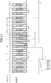
- (1) of FIG. 12 is a diagram illustrating an example of a timing chart illustrating the illumination timing of pulsed light Lc emitted from the light source 51.
- (2) of FIG. 12 is a diagram illustrating an example of a timing chart for explaining the exposure timing and the read timing of the reading unit 243 when the image sensor of the imaging unit 24 is a CCD image sensor. Each pulsed light is output with the same pulse width (illumination period).
- the pulsed light Lc is emitted in a cycle longer than the frame cycle of the imaging unit 24.
- the imaging unit 24 employs the global shutter method, so that all the pixel signals of the light receiving unit 242 from the same frame are exposed in the same period and read at the same timing. For example, regarding the frame (N - 2), after being exposed in an exposure period A (N - 2) , a pixel signal D (N - 2) corresponding to a pixel signal of all the pixels is read at a time R (N-2) .
- each illumination period of the pulsed light Lc is not overlapped with the read timing of each pixel signal, so that in the same manner as the generation processing of the illumination time pixel signal with respect to a non-overlap line in the first embodiment, the illumination time pixel signal is generated based on a pixel signal of a non-overlap line in the pixel signal of a frame that is read immediately after the illumination period of the pulsed light in which the illumination time pixel signal is generated.
- the illumination time pixel signal is calculated by using the formula (7) for each pixel x in any horizontal line V.
- Pixel x of V ⁇ th line exposed with pulsed light Lc 3 Pixel x of V ⁇ th line of D N ⁇ 2 exposed with pulsed light Lc 3
- an illumination time pixel signal of an overlap pixel row is generated by synthesizing a pixel signal of the overlap line that is read at an overlap timing overlapping with the illumination period and a pixel signal of an overlap line in a pixel signal of a frame immediately after the overlap timing.
- the pixel signals D (N - 2) , D N , and D (N + 1) among the pixel signals D (N - 2) to D (N + 1) are darkish images because illumination of the pulsed light is performed once in each of the exposure periods A (N - 1)) , A N , and A (N + 1) .
- the pixel signal D (N - 1) among the pixel signals D (N - 2) to D (N + 1) is a pitch-dark image without exposure because illumination of the pulsed light is not performed during the exposure period A (N - 1) .
- the illumination time pixel signal that is actually output from the image processing unit 45 corresponds to a pixel signal generated when all the pixels in the light receiving unit 242 are exposed with the pulsed light, so that no variation occurs in the brightness.
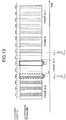
- FIG. 13 is a diagram illustrating an example of a timing chart illustrating the illumination timing of the pulsed light Ld emitted from the light source 51.
- (2) of FIG. 13 is a diagram illustrating an example of a timing chart for explaining the exposure timing and the read timing of the reading unit 243 when the image sensor of the imaging unit 24 is a CCD image sensor.
- Each pulsed light is output with the same pulse width (illumination period).
- an illumination time pixel signal is generated for the pulsed light Ld 6 in (1) of FIG. 13 .
- the illumination period T Ld6 of the pulsed light Ld 6 does not overlap with the read timing of each pixel signal.
- the illumination time pixel signal is generated based on the pixel signal of the horizontal line V corresponding to each of the pixel signals D (N - 1) of the frame (N - 1) that is read at the read timing immediately after the illumination timing of the pulsed light Ld 6 .
- the exposure period of the frame (N - 1) includes a part of period of the pulsed light Ld 4 and the entire illumination periods of the pulsed light Ld 5 and Ld 7 in addition to the illumination period T Ld6 of the pulsed light Ld 6 . Therefore, in the same manner as in the case of the non-overlap line in the second embodiment, the image processing unit 45 calculates the illumination time pixel signal by using the formula (8) which takes into account a ratio between the illumination period of the pulsed light Ld 6 and the illumination period of other pulsed light Ld 4 , Ld 5 , and Ld 7 .
- an illumination time pixel signal is generated for the pulsed light Ld 4 in (1) of FIG. 13 .
- the illumination period T Ld4 of the pulsed light Ld 4 overlaps with the read timing R (N - 2) in the frame (N - 2).
- the illumination time pixel signal is generated based on the pixel signal of the horizontal line V in the pixel signal D (N - 2) of the frame (N - 2) read at an overlap timing overlapping with the illumination timing of the pulsed light Ld 4 and the pixel signal of the horizontal line V in the pixel signal D (N - 1) of the frame (N - 1) immediately after the overlap timing.
- the exposure period of the frame (N - 2) includes the illumination periods of the pulsed light Ld 1 to Ld 3 in addition to the first half of the illumination period T Ld4 of the pulsed light Ld 4 .
- the exposure period of the frame (N - 1) includes the illumination periods of the pulsed light Ld 5 to Ld 7 in addition to the second half of the illumination period T Ld4 of the pulsed light Ld 4 . Therefore, the image processing unit 45 performs calculation for the frame (N - 2) and the frame (N - 1) respectively in view of ratios between the illumination period of the pulsed light Ld 4 and the illumination periods of the other pulsed light for each pixel x of any horizontal line V, and synthesizes the calculation results.
- the illumination time pixel signal of each pixel x of the horizontal line V is calculated by using the formula (9).
- the fractional terms (exposure time ratio) of the arithmetic expression vary for each horizontal line.
- the fractional terms of the arithmetic expression are fixed values.
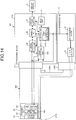
- FIG. 14 is a block diagram schematically illustrating a configuration of an endoscope system 201 according to the third embodiment.
- the endoscope system 201 includes a processing device 204 instead of the processing device 4 illustrated in FIG. 2 .
- the endoscope system 201 does not have the voice input device 3, the cord 31, and the connector 311 illustrated in FIG. 2 .
- a connector 233A of a branch cord 234A of a universal cord of an endoscope 202 is configured to be connected to the light source device 5, and does not have the splitter 53 and the light detector 54 illustrated in FIG. 2 .
- a control unit 43A of the processing device 204 includes a light source controller 431A that controls the pulse width (illumination period) of the pulsed light output from the light source 51 based on the brightness of the pixel signal read by the imaging unit 24.
- the light source controller 431A performs control in which the illumination timing of the pulsed light of the light source 51 is synchronized with the frame cycle of the imaging unit 24.
- a timing detecting unit 44A detects a line where the illumination timing and the illumination period in which the illumination time pixel signal is generated and the read timing overlap with each other from among the pixel signals read from the imaging unit 24 based on a light source control signal of the light source controller 431A and the vertical synchronizing signal and the horizontal synchronizing signal attached to the pixel signal output from the imaging unit 24.
- the timing detecting unit 44A detects the illumination timing and the illumination period of the pulsed light from the light source 51 and the read timing of each horizontal line of the light receiving unit 242 by the reading unit 243.
- the timing detecting unit 44A detects a horizontal line, where the read timing overlaps with the illumination period in which the illumination time pixel signal is generated, as an overlap line from among the pixel signals read from the reading unit 243.
- FIG. 16A is a timing chart illustrating a processing state of the imaging unit 24 and each element of the processing device 204 according to the third embodiment.
- (1) of FIG. 16A is a timing chart illustrating an output of the vertical synchronizing signal in the CMOS image sensor constituting the imaging unit 24.
- A(2) of FIG. 16 is a timing chart illustrating a data output from the reading unit 243 of the CMOS image sensor.
- (3) of FIG. 16A is a timing chart illustrating an exposure state of the CMOS image sensor.
- (4) of FIG. 16A is an exemplary timing chart illustrating the illumination timing of the pulsed light (PWM) emitted from the light source 51.
- PWM pulsed light
- FIG. 16A is a timing chart illustrating a pixel signal of each frame input into the memory 46.
- (6) of FIG. 16A is a timing chart illustrating the illumination time pixel signal generated by the image processing unit 45.
- FIG. 16B is a schematic diagram for explaining an image of an illumination time pixel signal (G PWM2 ) corresponding to pulsed light (PWM2) generated by the image processing unit 45.
- the pulse signal of each pulsed light (PWM1, PWM2) rises in a period Te after the rise of the corresponding vertical signal.
- the non-overlap lines are the horizontal line 1 to the horizontal line e and the horizontal line (f + 1) to the last horizontal line j among the horizontal lines V (V is an integer.
- V 1, ⁇ , e, ⁇ , h ⁇ , f, ⁇ , i, ⁇ , g, ⁇ , j).
- the overlap lines are the horizontal line (e + 1) to the horizontal line f.
- the generation of the illumination time pixel signal for the horizontal lines 1 to e among the non-overlap lines will be described.
- the entire illumination period T 6 of the pulsed light PWM2, in which the illumination time pixel signal is generated is included in the exposure period of the horizontal lines 1 to e of the frame (M + 1).
- the other pulsed is not emitted in the exposure period of the frame (M + 1).
- the image processing unit 45 directly outputs data of each pixel of the horizontal lines 1 to e of the pixel signal D (M + 1) of the frame (M + 1) that is read at the read timing immediately after the illumination timing of the pulsed light PWM2 as the illumination time pixel signal of the pulsed light PWM2 of the horizontal lines 1 to e (see area A in FIG. 16B ). Also for the horizontal lines (g + 1) to j, the entire illumination period T 6 of the pulsed light (PWM2) is included in the exposure period of the horizontal lines (g + 1) to j of the frame M and the other pulsed light is not emitted in the exposure period of the frame M.
- the image processing unit 45 directly outputs data of each pixel of the horizontal lines (g + 1) to j of the pixel signal D M of the frame M that is read at the read timing immediately after the illumination timing of the pulsed light PWM2 as the illumination time pixel signal of the pulsed light PWM2 of the horizontal lines (g + 1) to j (see area D in FIG. 16B ).
- the generation of the illumination time pixel signal for the horizontal line i (f + 1 ⁇ i ⁇ g) among the non-overlap lines will be described.
- the illumination period T 5 of a part of the pulsed light PWM1 that is emitted before the pulsed light PWM2 is included in the exposure period of the horizontal line i of the frame M.
- the image processing unit 45 calculates the illumination time pixel signal by using the formula (10) which takes into account a ratio between the illumination period T 6 of the pulsed light PWM2 and the illumination period T 5 of a part of the pulsed light (PWM1) that is emitted before the pulsed light PWM2 for the pixel signal of the horizontal line i of the pixel signal D M of the frame M that is read at the read timing immediately after the illumination timing of the pulsed light PWM2.
- the area C in FIG. 16B corresponding to the horizontal line i (f + 1 ⁇ i ⁇ g) is formed by a signal obtained by applying a gain correction to the pixel signal D M .
- Pixel x of i ⁇ th line exposed with pulsed light PWM 2 Pixel x of i ⁇ th line of D M ⁇ T 6 T 5 + T 6
- the image processing unit 45 For the horizontal line h, the image processing unit 45 generates the illumination time pixel signal based on the pixel signal of the horizontal line h in the pixel signal D M of the frame M read at an overlap timing overlapping with the illumination timing of the pulsed light PWM2 and the pixel signal of the horizontal line h in the pixel signal D (M + 1) of the frame (M + 1) immediately after the overlap timing.
- the exposure period of the horizontal line h of the frame M includes the second half period T 1 of the illumination period of the pulsed light (PWM1) emitted before the pulsed light (PWM2) in addition to the first half period T 2 of the illumination period T 6 of the pulsed light (PWM2). Further, the exposure period of the horizontal line h of the frame (M + 1) includes the first half period T 4 of the illumination period of the pulsed light PWM3 emitted after the pulsed light PWM2 in addition to the second half period T 3 of the illumination period T 6 of the pulsed light PWM2.
- the image processing unit 45 calculates the pixel signal of the horizontal line h in receiving only the pulsed light PWM2 in the frame M in view of a ratio between the first half period T 2 of the illumination period of the pulsed light PWM2 and the second half period T 1 of the illumination period of the pulsed light PWM1 before the pulsed light PWM2 for each pixel x of the horizontal line h. Then, the image processing unit 45 calculates the pixel signal of the horizontal line h in receiving only the pulsed light PWM2 in the frame (M + 1) in view of a ratio between the second half period T 3 of the illumination period of the pulsed light PWM2 and the first half period T 4 of the illumination period of the pulsed light PWM3 following the pulsed light PWM2.
- the image processing unit 45 calculates the illumination time pixel signal of each pixel x of the horizontal line h by synthesizing the pixel signal of the horizontal line h in receiving only the pulsed light PWM2 in the frame M and the pixel signal of the horizontal line h in receiving only the pulsed light PWM2 in the frame (M + 1). Specifically, the illumination time pixel signal of each pixel x of the horizontal line h, which is an overlap line, is calculated by using the formula (11). Therefore, the area B in FIG. 16B corresponding to the horizontal line h (e + 1 ⁇ h ⁇ f) is formed by a synthesized signal of the pixel signal D M and pixel signal D (M + 1) .
- Pixel x of h ⁇ th line exposed with pulsed light PWM 2 Pixel x of h ⁇ th line of D M ⁇ T 2 T 1 + T 2 + Pixel x of h ⁇ th line of D M + 1 ⁇ T 3 T 3 + T 4
- the illumination time pixel signal may be calculated by considering whether each pixel is located in an overlap line or a non-overlap line and a ratio between an illumination period of pulsed light in which the illumination time pixel signal is generated and an illumination period of the other pulsed light included in the exposure period of the line. Also in the third embodiment, the display controller 47 may generate the display image signal based on the illumination time pixel signal generated by the image processing unit 45 in the same manner as in the first and second embodiments.
- the reading unit 243 only has to be able to perform exposure control and read control of the light receiving unit 242, so that the reading unit 243 does not necessarily have to be provided in the imaging unit 24 and the reading unit 243 may be provided in the previous stage of the image processing unit 45 of the processing device 4 or 204.
- the splitter 53 only has to be provided on a light path of the pulsed light emitted from the light source unit 51, and the light detector 54 only has to be provided at a position where the light split by the splitter 53 is received.
- the splitter 53 and the light detector 54 may be provided in an adapter 7 for connecting to the connector 233A of a universal cord 23A and to a connector 55 of the light source device 5.
- the adapter 7 includes a connector 71, a connector 72, a light guide cable 73, the splitter 53 provided on a propagation path of pulsed light L of the light guide cable 73, the light detector 54, a pulse signal cord 74, and a connector 75.
- the connector 71 is connected to the connector 55 of the light source device 5.
- the connector 72 is connected to the connector 223A of the universal cord 23A.
- the light guide cable 73 propagates the pulsed light L of the light source unit 51 to a light guide cable 235 of the universal cord 23A.
- the pulse signal cord 74 transmits a pulse signal Ep converted by the light detector 54 to a processing device 4B.
- the connector 75 is provided at an end portion of the pulse signal cord 74 and is connected to a connector 48B of the processing device 4B.
- a connector 48A is also illustrated.
- the connector 48A is connected with a connector 232A at an end portion of a branch cord 231A having a transmission cable of an image signal Eg.
- a processing device 4C, the light source device 5, and an integrated connector 233B at an end portion of a universal cord 23B are connected by an integrated adapter 7B.
- the splitter 53 and the light detector 54 may be provided in the integrated adapter 7B.
- a main body of the integrated adapter 7B includes the connector 71 for connecting to the connector 55 of the light source device 5, an integrated connector 76 for connecting to an integrated connector 48 of the processing device 4C, and an integrated connector 72B for connecting to the integrated connector 233B at an end portion of the universal cord 23B, in addition to the splitter 53 and the light detector 54.
- FIG. 17 and FIG. 18 illustrate only main elements.
- An execution program for each process executed in the image processing unit 45 and the other elements according to the embodiments may be provided by being recorded in a computer-readable recording medium such as a CD-ROM, a flexible disk, a CD-R, and a DVD (Digital Versatile Disk) as a file in an installable format or an executable format or may be provided by being stored on a computer connected to a network such as the Internet and being downloaded through the network. Further, the execution program may be provided or distributed through a network such as the Internet.
Landscapes
- Health & Medical Sciences (AREA)
- Life Sciences & Earth Sciences (AREA)
- Physics & Mathematics (AREA)
- Engineering & Computer Science (AREA)
- Surgery (AREA)
- Optics & Photonics (AREA)
- Multimedia (AREA)
- Signal Processing (AREA)
- Medical Informatics (AREA)
- Veterinary Medicine (AREA)
- Radiology & Medical Imaging (AREA)
- Nuclear Medicine, Radiotherapy & Molecular Imaging (AREA)
- Biomedical Technology (AREA)
- Heart & Thoracic Surgery (AREA)
- Biophysics (AREA)
- Molecular Biology (AREA)
- Animal Behavior & Ethology (AREA)
- General Health & Medical Sciences (AREA)
- Public Health (AREA)
- Pathology (AREA)
- General Physics & Mathematics (AREA)
- Astronomy & Astrophysics (AREA)
- Otolaryngology (AREA)
- Physiology (AREA)
- Pulmonology (AREA)
- Computing Systems (AREA)
- Theoretical Computer Science (AREA)
- Endoscopes (AREA)
- Studio Devices (AREA)
- Instruments For Viewing The Inside Of Hollow Bodies (AREA)
Abstract
Description
- The present invention relates to a processing device for processing a pixel signal, an imaging device, and an endoscope system.
- Conventionally, in the medical field, an endoscope system is used to observe the inside of a subject. In general, the endoscope system captures an in-vivo image by inserting a flexible insertion unit having an elongated shape into the subject such as a patient, intermittently emitting illumination light from the distal end of the insertion unit, and receiving reflected light of the illumination light by using an imaging unit at a distal end portion of the insertion unit. The in-vivo image captured in this way is displayed on a display of the endoscope system.
- When imaging is performed under intermittent illumination, a variation in brightness occurs between images depending on an exposure timing of an image sensor, so that the images may flick when the images are displayed on the display. In particular, when employing a CMOS (Complementary Metal Oxide Semiconductor) image sensor and applying a rolling shutter method that changes timing of exposure and reading for each horizontal line, an exposure timing varies for each horizontal line in one imaging period, so that luminance unevenness easily occurs.
- In order to address such a situation, conventionally, a technique is proposed that generates a display image by removing areas having luminance greater than or equal to a predetermined threshold value from a frame image (for example, see Patent Literature 1). In addition to the technique described in
Patent Literature 1 that removes part of an image, a technique is also proposed that can secure a certain level of luminance in the entire area of an image by causing a light source to emit illumination light in a period common to all pixels in an exposure period of each pixel of an image sensor (for example, see Patent Literature 2). -
- Patent Literature 1:
JP 2010-135921 A - Patent Literature 2:
JP 2009-136447 A - However, to secure an enough period to be able to commonly expose all the pixels, it is required to lower the frame rate or increase reading speed. In view of quality of a moving image and heat generation of an image sensor, there is a case in which it is required to control so that illumination timing overlaps with read timing of the image sensor. Further, for example, in a stroboscopic observation device that performs illumination using pulsed light by synchronizing the pulsed light with a vibration frequency of vocal cords, illumination timing and read timing are asynchronous, so that even when an enough period to be able to commonly expose all the pixels is secured, there is a case in which the illumination timing overlaps with the read timing. In this case, an exposure amount varies between images and brightness variation between images cannot be eliminated, and thus, image quality may not be maintained.
- The present invention has been made in view of the foregoing, and an object of the present invention is to provide a processing device, an imaging device, and an endoscope system that can maintain image quality even if pulsed light is emitted at any timing with respect to the read timing of the image sensor.
- In order to solve the above described problem and achieve the object, a processing device according to the invention processes a pixel signal of a plurality of pixels configured to receive light from a subject illuminated with pulsed light and to perform photoelectric conversion on the received light to generate the pixel signal. The processing device includes a signal processing unit configured to generate, from the pixel signal, an illumination time pixel signal that is a pixel signal generated when the plurality of pixels is exposed in an illumination period of the pulsed light, according to an overlapping state between the illumination period of the pulsed light and read timing of the pixel signal.
- The processing device according to the invention further includes a storage unit configured to store the pixel signal for each frame in accordance with a matrix arrangement of the plurality of pixels. The signal processing unit is configured to generate the illumination time pixel signal corresponding to the illumination period of the pulsed light for each frame for each illumination period of the pulsed light from the pixel signal of a plurality of continuous frames stored in the storage unit.
- The processing device according to the invention further includes a detecting unit configured to acquire the read timing and the illumination period of the pulsed light and detects a pixel row in which the read timing overlaps with the illumination period of the pulsed light, in which the illumination time pixel signal is generated, from the pixel signal as an overlap pixel row.
- In the processing device according to the invention, the signal processing unit is configured to generate an illumination time pixel signal of the overlap pixel row based on a pixel signal of the overlap pixel row read at an overlap timing that overlaps with the illumination period of the pulsed light and a pixel signal of the overlap pixel row in the pixel signal of a frame that is read after the overlap timing.
- In the processing device according to the invention, for a non-overlap pixel row which is a pixel row other than the overlap pixel row, the signal processing unit is configured to generate the illumination time pixel signal based on a pixel signal of the non-overlap pixel row in the pixel signal of a frame that is read after the illumination period of the pulsed light in which the illumination time pixel signal is generated.
- The processing device according to the invention further includes a display controller configured to generate a display image signal to be displayed by a display device from an illumination time pixel signal of a plurality of frames generated by the signal processing unit in accordance with a display cycle of the display device connected to the processing device.
- An imaging device according to the invention includes: a light receiving unit having a plurality of pixels arranged in a matrix form, the plurality of pixels being configured to receive light from a subject illuminated with pulsed light and to perform photoelectric conversion on the received light to generate a pixel signal; a reading unit configured to perform exposure on the plurality of pixels of the light receiving unit and to read the pixel signal from the plurality of pixels of the light receiving unit; and a signal processing unit configured to generate, from the pixel signal read by the reading unit, an illumination time pixel signal that is a pixel signal generated when the plurality of pixels is exposed in an illumination period of the pulsed light, according to an overlapping state between the illumination period of the pulsed light and read timing of the pixel signal read by the reading unit.
- The imaging device according to the invention further includes a storage unit configured to store the pixel signal for each frame in accordance with a matrix arrangement of the plurality of pixels in the light receiving unit. The signal processing unit is configured to generate the illumination time pixel signal corresponding to the illumination period of the pulsed light for each frame for each illumination period of the pulsed light from the pixel signal of a plurality of continuous frames stored in the storage unit.
- The imaging device according to the invention further includes a detecting unit configured to acquire the read timing and the illumination period of the pulsed light and detects a pixel row in which the read timing overlaps with the illumination period of the pulsed light, in which the illumination time pixel signal is generated, from the pixel signal as an overlap pixel row.
- In the imaging device according to the invention, the signal processing unit is configured to generate an illumination time pixel signal of the overlap pixel row based on a pixel signal of the overlap pixel row read at an overlap timing that overlaps with the illumination period of the pulsed light and a pixel signal of the overlap pixel row in the pixel signal of a frame that is read after the overlap timing.
- In the imaging device according to the invention, for a non-overlap pixel row which is a pixel row other than the overlap pixel row, the signal processing unit is configured to generate the illumination time pixel signal based on a pixel signal of the non-overlap pixel row in the pixel signal of a frame that is read after the illumination period of the pulsed light in which the illumination time pixel signal is generated.
- The imaging device according to the invention further includes a display controller configured to generate a display image signal to be displayed by a display device from an illumination time pixel signal of a plurality of frames generated by the signal processing unit in accordance with a display cycle of the display device connected to the imaging device.
- In the imaging device according to the invention, the light receiving unit and the reading unit are constituted by a CMOS image sensor.
- In the imaging device according to the invention, the light receiving unit and the reading unit are constituted by a CCD image sensor.
- An endoscope system according to the invention includes: a light source configured to emit pulsed light to illuminate a subject; a light receiving unit having a plurality of pixels arranged in a matrix form, the plurality of pixels being configured to receive light from the subject illuminated with the pulsed light emitted from the light source and to perform photoelectric conversion on the received light to generate a pixel signal; a reading unit configured to perform exposure on the plurality of pixels of the light receiving unit and to read the pixel signal from the plurality of pixels of the light receiving unit; and a signal processing unit configured to generate, from the pixel signal read by the reading unit, an illumination time pixel signal that is a pixel signal generated when the plurality of pixels is exposed in an illumination period of the pulsed light, according to an overlapping state between the illumination period of the pulsed light emitted from the light source and read timing of the pixel signal read by the reading unit.
- The endoscope system according to the invention further includes a storage unit configured to store the pixel signal for each frame in accordance with a matrix arrangement of the plurality of pixels in the light receiving unit. The signal processing unit is configured to generate the illumination time pixel signal corresponding to the illumination period of the pulsed light for each frame for each illumination period of the pulsed light from the pixel signal of a plurality of continuous frames stored in the storage unit.
- The endoscope system according to the invention further includes a detecting unit configured to acquire the read timing and the illumination period of the pulsed light and detects a pixel row in which the read timing overlaps with the illumination period of the pulsed light, in which the illumination time pixel signal is generated, from the pixel signal as an overlap pixel row.
- In the endoscope system according to the invention, the signal processing unit is configured to generate an illumination time pixel signal of the overlap pixel row based on a pixel signal of the overlap pixel row read at an overlap timing that overlaps with the illumination period of the pulsed light and a pixel signal of the overlap pixel row in the pixel signal of a frame that is read after the overlap timing.
- In the endoscope system according to the invention, for a non-overlap pixel row which is a pixel row other than the overlap pixel row, the signal processing unit is configured to generate the illumination time pixel signal based on a pixel signal of the non-overlap pixel row in the pixel signal of a frame that is read after the illumination period of the pulsed light in which the illumination time pixel signal is generated.
- The endoscope system according to the invention further includes a display controller configured to generate a display image signal to be displayed by a display device from an illumination time pixel signal of a plurality of frames generated by the signal processing unit in accordance with a display cycle of the display device connected to the endoscope system.
- In the endoscope system according to the invention, the subject is vocal cords.
- The endoscope system according to the invention further includes: a voice input unit to which a voice is configured to be input; a vibration cycle detecting unit configured to detect a vibration cycle of the voice input into the voice input unit; and a light source controller configured to control an illumination timing and the illumination period of the pulsed light from the light source in synchronization with the vibration cycle of the voice detected by the vibration cycle detecting unit.
- The endoscope system according to the invention further includes a light source controller configured to: synchronize an illumination timing of the pulsed light from the light source with a frame cycle of the light receiving unit and the reading unit; and control the illumination period of the pulsed light from the light source based on the pixel signal read by the reading unit.
- In the endoscope system according to the invention, the light receiving unit and the reading unit are constituted by a CMOS image sensor.
- In the endoscope system according to the invention, the light receiving unit and the reading unit are constituted by a CCD image sensor.
- According to the present invention, an illumination time pixel signal is generated from a pixel signal of a plurality of pixels that has received light from a subject irradiated with pulsed light, according to an overlapping state between illumination timing of the pulsed light and read timing of the pixel signal. The illumination time pixel signal is a pixel signal generated when the plurality of pixels is exposed in an illumination period of the pulsed light. With this feature, it is possible to maintain image quality even if the pulsed light is emitted at any timing with respect to the read timing of an image sensor.
-
-
FIG. 1 is a schematic diagram illustrating a schematic configuration of an endoscope system according to a first embodiment of the present invention. -
FIG. 2 is a block diagram schematically illustrating a configuration of the endoscope system illustrated inFIG. 1 . -
FIG. 3 is a diagram illustrating an example of a configuration of an electric circuit constituting a light detector illustrated inFIG. 2 . -
FIG. 4 is a timing chart illustrating an ideal image output timing in an imaging unit with respect to an illumination timing of pulsed light. -
FIG. 5 is a diagram for explaining an illumination timing of pulsed light by a light source device and exposure and read timings by a reading unit illustrated inFIG. 2 . -
FIG. 6 is a timing chart illustrating a processing state of the imaging unit and each element of a processing device illustrated inFIG. 2 . -
FIG. 7 is a diagram for explaining generation processing of a display image signal by a display controller illustrated inFIG. 2 . -
FIG. 8 is a diagram for explaining the generation processing of the display image signal by the display controller illustrated inFIG. 2 . -
FIG. 9 is a diagram for explaining an illumination timing of pulsed light by a light source and exposure and read timings by a reading unit according to a second embodiment. -
FIG. 10 is a timing chart illustrating a processing state of an imaging unit and each element of a processing device according to the second embodiment. -
FIG. 11 is a diagram for explaining generation processing of a display image signal by a display controller according to the second embodiment. -
FIG. 12 is a diagram for explaining an illumination timing of pulsed light by a light source and exposure and read timings by a reading unit when a CCD image sensor is employed in the first and second embodiments. -
FIG. 13 is a diagram for explaining another example of an illumination timing of pulsed light by a light source and exposure and read timings by a reading unit when a CCD image sensor is employed in the first and second embodiments. -
FIG. 14 is a block diagram schematically illustrating a configuration of an endoscope system according to a third embodiment. -
FIG. 15 is a diagram for explaining an illumination timing of pulsed light by a light source and exposure and read timings by a reading unit illustrated inFIG. 14 . -
FIG. 16A is a timing chart illustrating a processing state of an imaging unit and each element of a processing device according to the third embodiment. -
FIG. 16B is a schematic diagram for explaining an image of an illumination time pixel signal corresponding to pulsed light generated by an image processing unit in the third embodiment. -
FIG. 17 is a schematic diagram illustrating a case in which a splitter and a light detector are provided in an adaptor. -
FIG. 18 is a block diagram schematically illustrating another case in which a splitter and a light detector are provided in an adaptor. - Reference will be made below to an endoscope system as modes for carrying out the present invention (hereinafter referred to as "embodiment(s)"). The present invention is not limited by the embodiments. The same reference signs are used to designate the same elements throughout the drawings. The drawings are schematic, and it is noted that the relation between the thickness and the width of each member and the ratio of the size of each member are different from the reality. The size and the ratio of the same element may be different in a different drawing.
-
FIG. 1 is a schematic diagram illustrating a schematic configuration of an endoscope system according to a first embodiment of the present invention. As illustrated inFIG. 1 , theendoscope system 1 according to the first embodiment includes an endoscope 2 (scope) which is introduced into a subject and captures an image inside the subject to generate an image signal of inside of the subject, avoice input device 3 to which a voice is input, alight source device 5 that generates pulsed light as illumination light (observation light) of theendoscope 2, aprocessing device 4 which performs predetermined image processing on the image signal captured by theendoscope 2 and controls each element of theendoscope system 1, and adisplay device 6 which displays an image corresponding to the image signal on which theprocessing device 4 performs the image processing. - The
endoscope 2 includes aninsertion unit 21 that is inserted into the subject, an operatingunit 22 which is provided at a proximal end portion of theinsertion unit 21 and held by an operator, and a flexibleuniversal cord 23 that extends from the operatingunit 22. - The
insertion unit 21 is realized by using an illumination fiber (light guide cable), an electric cable, and the like. Theinsertion unit 21 includes adistal end portion 211 including an imaging unit incorporating a CMOS image sensor as an image sensor that captures an image inside the subject, abendable bending portion 212 formed by a plurality of bending pieces, and aflexible tube portion 213 having flexibility provided at the proximal end portion of the bendingportion 212. Thedistal end portion 211 is provided with an illumination unit that illuminates inside the subject through an illumination lens, an observation unit that captures an image inside the subject, anopening portion 214 through which a processing tool channel passes, and an air/water nozzle (not illustrated inFIG. 1 ). - The operating
unit 22 includes a bendingknob 221 that bends the bendingportion 212 in a vertical direction and a horizontal direction, a treatmenttool insertion portion 222 through which treatment tools such as biopsy forceps and a laser scalpel are inserted into a body cavity of the subject, and a plurality ofswitch units 223 for operating peripheral apparatuses such as theprocessing device 4, thelight source device 5, an air supply device,
a water supply device, and a gas supply device. A treatment tool inserted from the treatmenttool insertion portion 222 is exposed from theopening portion 214 at the distal end of theinsertion unit 21 through a treatment tool channel provided inside theinsertion unit 21. - The
universal cord 23 is formed by using an illumination fiber, an electric cable, and the like. Theuniversal cord 23 is split at its proximal end. An end portion of onebranch cord 231 is aconnector 232 and the proximal end of theother branch cord 234 is aconnector 233. Theconnector 232 is attachable to and detachable from theprocessing device 4. Theconnector 233 is attachable to and detachable from thelight source device 5. Theuniversal cord 23 transmits an image signal captured by the imaging unit provided in thedistal end portion 211 to theprocessing device 4 through theconnector 232. Theuniversal cord 23 propagates the illumination light emitted from thelight source device 5 to thedistal end portion 211 through theconnector 233, the operatingunit 22, and theflexible tube portion 213. - The
voice input device 3 is input with a voice issued from vocal cords when the subject is the vocal cords. A distal end of acord 31 is connected to thevoice input device 3 and aconnector 311 at the proximal end of thecord 31 is attachable to and detachable from theprocessing device 4. Thevoice input device 3 outputs the input voice to theprocessing device 4 through thecord 31 and theconnector 311. - The
processing device 4 performs predetermined image processing on an imaging signal in the subject which is captured by the imaging unit at thedistal end portion 211 of theendoscope 2 and input through theuniversal cord 23. Theprocessing device 4 controls each element of theendoscope system 1 based on various instruction signals transmitted from theswitch units 223 in the operatingunit 22 of theendoscope 2 through theuniversal cord 23. - The
light source device 5 is formed by using a light source that emits pulse-shaped white light, a condenser lens, and the like. Thelight source device 5 supplies pulse-shaped white light from a white light source to theendoscope 2 connected through theconnector 232 and the illumination fiber of theuniversal cord 23 as illumination light for illuminating inside of the subject which is a subject. A part of the pulsed light emitted from thelight source device 5 is split at theconnector 233 and formed into a pulse signal, and thereafter input into theprocessing device 4 through thebranch cords connector 232. - The
display device 6 is formed by using a display using a liquid crystal or an organic EL (Electro Luminescence). Thedisplay device 6 displays various information including an image corresponding to a display image signal on which predetermined image processing is performed by theprocessing device 4 through animage cable 61. Thereby, an operator can observe a desired position in the subject and determine characteristics of the position by operating theendoscope 2 while seeing the image (in-vivo image) displayed by thedisplay device 6. - Next, configurations of the
endoscope 2, thevoice input device 3, theprocessing device 4, and thelight source device 5, which are described inFIG. 1 , will be described.FIG. 2 is a block diagram schematically illustrating the configuration of theendoscope system 1. - The
endoscope 2 includes animaging unit 24 at thedistal end portion 211. Theimaging unit 24 includes anoptical system 241 such as an objective lens arranged on a light receiving surface side of alight receiving unit 242 described below, thelight receiving unit 242 that generates a pixel signal representing the inside of the subject from an optical image formed on the light receiving surface, and areading unit 243. - The
light receiving unit 242 has a plurality of pixels arranged on the light receiving surface. The plurality of pixels is configured to receive light from the subject illuminated with the pulsed light from thelight source device 5 and to perform photoelectric conversion on the received light to generate a pixel signal. A plurality of pixels is arranged in a matrix form on thelight receiving unit 242. In thelight receiving unit 242, a plurality of pixel rows (horizontal lines), in each of which two or more pixels are arranged along a horizontal direction, is arranged so as to be lined up in a vertical direction. Thelight receiving unit 242 generates a pixel signal representing the inside of the subject from the optical image formed on the light receiving surface. - The
reading unit 243 performs exposure on the plurality of pixels in thelight receiving unit 242 and reading of the pixel signal from the plurality of pixels. Thelight receiving unit 242 and thereading unit 243 are constituted by, for example, a CMOS image sensor and can perform exposure and reading for each horizontal line. Thereading unit 243 performs an imaging operation, which performs exposure and reading, from a first horizontal line and generates a pixel signal by a rolling shutter method that performs charge reset, exposure, and reading by shifting timing for each horizontal line. Therefore, in theimaging unit 24, even in one imaging period (frame), the exposure timing and the read timing vary for each horizontal line. Thereading unit 243 outputs the pixel signal read from the plurality of pixels of thelight receiving unit 242 to theprocessing device 4 through a cable (not illustrated in the drawings) and theconnector 232. A vertical synchronizing signal and a horizontal synchronizing signal attached to the pixel signal output from the CMOS image sensor are also input into atiming detecting unit 44 described later. - Next, the
processing device 4 will be described. Theprocessing device 4 includes aninput unit 41, a vibrationalfrequency detecting unit 42, acontrol unit 43, atiming detecting unit 44, an image processing unit 45 (signal processing unit), amemory 46, and adisplay controller 47. - The
input unit 41 is realized by using operation devices such as a mouse, a keyboard, and a touch panel and receives input of various instruction information of theendoscope system 1. Specifically, theinput unit 41 receives subject information (for example, ID, date of birth, and name), identification information (for example, ID and examination corresponding items) of theendoscope 2, and various instruction information such as examination content. - The vibrational
frequency detecting unit 42 detects the frequency of a voice which is input into thevoice input device 3 and input into theprocessing device 4 through thecord 31 and theconnector 311. The voice is issued from vocal cords which are the subject. The vibrationalfrequency detecting unit 42 outputs the detected frequency of the voice to thecontrol unit 43. - The
control unit 43 is realized by using a CPU and the like. Thecontrol unit 43 controls a processing operation of each element of theprocessing device 4. Thecontrol unit 43 controls operation of theprocessing device 4 by transmitting instruction information and data to each element of theprocessing device 4. Thecontrol unit 43 is connected to theimaging unit 24 and thelight source device 5 through each cable. Thecontrol unit 43 includes alight source controller 431 that controls operation of thelight source device 5. Thelight source controller 431 controls an illumination timing and an illumination period of the pulsed light from alight source 51 in synchronization with the frequency of the voice detected by the vibrationalfrequency detecting unit 42. Thecontrol unit 43 also controls operation of theimaging unit 24. - The
timing detecting unit 44 detects the illumination timing and the illumination period of the pulsed light based on a pulse signal which is input from thelight source device 5 and which corresponds to the pulsed light from thelight source device 5. Thetiming detecting unit 44 detects the read timing of the pixel signal read by thereading unit 243 for each horizontal line based on the vertical synchronizing signal and the horizontal synchronizing signal attached to the pixel signal output from theimaging unit 24. Thetiming detecting unit 44 acquires the read timing, the illumination timing, and the illumination period and detects a horizontal line, where the read timing overlaps with an illumination period in which an illumination time pixel signal described later is generated, as an overlap line from among the pixel signals read by thereading unit 243. - The
image processing unit 45 performs predetermined image processing on the pixel signal of a plurality of pixels read by thereading unit 243 of theimaging unit 24. For example, theimage processing unit 45 performs image processing including at least optical black subtraction processing, white balance (WB) adjustment processing, image signal synchronization processing when the image sensor is a Bayer array, color matrix calculating processing, gamma correction processing, color reproduction processing, and edge enhancement processing on the pixel signal. - The
image processing unit 45 generates the illumination time pixel signal which is a pixel signal in a case in which a plurality of pixels is exposed in the illumination period of the pulsed light from thelight source device 5 from the pixel signal of a plurality of pixels read by thereading unit 243 of theimaging unit 24 according to an overlapping state between the illumination timing and the illumination period of the pulsed light of thelight source device 5 and the read timing of the pixel signal read by thereading unit 243. Theimage processing unit 45 generates the illumination time pixel signal corresponding to the illumination period of illumination for each frame for each illumination timing from pixel signals of a plurality of continuous frames stored in thememory 46 described later. For the overlap line, theimage processing unit 45 generates the illumination time pixel signal based on a pixel signal of the overlap line read at an overlap timing that overlaps with the illumination period of the pulsed light and a pixel signal of an overlap line in a pixel signal of a frame that is read first after the overlap timing. For a non-overlap line which is a horizontal line other than the overlap line, theimage processing unit 45 generates the illumination time pixel signal based on a pixel signal of a non-overlap pixel line in a pixel signal of a frame that is read first after the illumination period of the pulsed light in which the illumination time pixel signal is generated. - The
memory 46 is realized by using volatile memory and/or non-volatile memory and stores various programs to operate theprocessing device 4 and thelight source device 5. Thememory 46 temporarily records information that is being processed by theprocessing device 4. Thememory 46 stores the pixel signal read by thereading unit 243 for each frame in accordance with a matrix arrangement of a plurality of pixels in thelight receiving unit 242. Thememory 46 stores the illumination time pixel signal generated by theimage processing unit 45 for each frame. Thememory 46 may be formed by using a memory card or the like attached from the outside of theprocessing device 4. - The
display controller 47 generates display image data to be displayed by thedisplay device 6 from the illumination time pixel signals of a plurality of frames generated by theimage processing unit 45 in accordance with a display cycle of thedisplay device 6. Thedisplay controller 47 selects display image data from among the illumination time pixel signals of a plurality of frames generated by theimage processing unit 45 for each display cycle of thedisplay device 6. Alternatively, thedisplay controller 47 generates a display image signal by synthesizing the illumination time pixel signals of a plurality of frames generated by theimage processing unit 45 for each display cycle of thedisplay device 6. Thedisplay controller 47 converts the display image data from a digital signal to an analog signal, changes image data of the converted analog signal into a high-definition television format or the like, and then outputs the image data to thedisplay device 6. - Next, the
light source device 5 will be described. Thelight source device 5 includes thelight source 51 and alight source driver 52. - The
light source 51 is formed by using a light source such as a white LED that emits pulse-shaped white light and an optical system such as a condenser lens. Thelight source 51 generates the illumination light to be supplied to theendoscope 2. - The
light source driver 52 supplies a predetermined electric power to thelight source 51 under control of thelight source controller 431. Thereby, the light generated from thelight source 51 is emitted to the subject from anillumination window 211a of thedistal end portion 211 of theinsertion unit 21 through theconnector 233 and theuniversal cord 23. Theimaging unit 24 is arranged near theillumination window 211a. - The
connector 233 includes asplitter 53 for splitting a part of the pulsed light generated from thelight source 51 and inputs the split light into alight detector 54 and thelight detector 54 that converts the pulsed light input from thesplitter 53 into a pulse signal. Thesplitter 53 is formed by an optical system such as a prism. Thelight detector 54 inputs the converted pulse signal into thetiming detecting unit 44 of theprocessing device 4 through thebranch cords connector 232.FIG. 3 is a diagram illustrating an example of a configuration of an electric circuit constituting thelight detector 54. As illustrated inFIG. 3 , when the pulsed light enters into thelight detector 54, a phototransistor Pt becomes an ON state and an electric current is input into an amplifier Ad through a capacitor C. Thereafter, a DC component is removed from the electric current and the electric current is amplified by the amplifier Ad, so that a pulse signal corresponding to the pulsed light is input into theprocessing device 4. -
FIG. 4 is a timing chart illustrating an ideal image output timing in theimaging unit 24 with respect to the illumination timing of the pulsed light. As illustrated inFIG. 4 , when each illumination timing of pulsed light (seeFIG. 4 (1)) corresponds with each exposure timing in the imaging unit 24 (seeFIG. 4 (2)), variation of brightness does not occur between a plurality of images to be output. On the other hand, in the first embodiment, the illumination timing of the pulsed light of thelight source 51 is controlled so as to be synchronized with the vibration frequency of a voice issued from vocal cords which are the subject, so that the illumination timing of the pulsed light does not necessarily correspond with the exposure timing in theimaging unit 24. In the first embodiment, a case will be described in which a light emitting cycle of the pulsed light is longer than a frame cycle of theimaging unit 24 and a display cycle in thedisplay device 6. First, with reference toFIG. 5 , the illumination timing of the pulsed light by thelight source 51 and the exposure timing and the read timing of thereading unit 243 will be described. -
FIG. 5 is a diagram for explaining the illumination timing of the pulsed light by thelight source 51 and the pixel exposure timing and the pixel signal read timing of thereading unit 243. (1) ofFIG. 5 is a diagram illustrating an example of a timing chart illustrating the illumination timing of the pulsed light emitted from thelight source 51. (2) ofFIG. 5 is a diagram illustrating an example of a timing chart for explaining the exposure timing and the read timing for a plurality of pixels by thereading unit 243. Each pulsed light is output with the same pulse width (illumination period). - The illumination timing of pulsed light L emitted from the
light source 51 is controlled so as to be synchronized with the vibration frequency of a voice issued from vocal cords which are the subject. For example, the pulsed light L is emitted from thelight source 51 for each cycle Cp illustrated in (1) ofFIG. 5 during a period TL. - The
imaging unit 24 uses a rolling shutter method that changes the exposure timing and the read timing for each horizontal line V (V is an integer. V = 1, ···, m, ···, s, ···, n, ···, t, ···, u, ···, j). Therefore, even for the pixel signals of the same frame, the exposure period and the read timing vary for each horizontal line. For example, for the pixels in the firsthorizontal line 1 of a frame (N - 1), thereading unit 243 reads the pixel signal at a time R1 after performing exposure in a period A1. Thereading unit 243 performs exposure and reading on the pixels of the following horizontal lines while shifting the timing in a time direction for each horizontal line. For the pixels in the last horizontal line j, thereading unit 243 performs exposure in a period Aj and reads the pixel signal at a time Rj. The pixel signal D(N - 1) of the frame (N - 1) illustrated inFIG. 5 is generated when the exposure on each horizontal line from thefirst line 1 to the last line j is sequentially performed and the pixel signals of the horizontal lines V are read in order from the first line in a period from the time R1 to the time Rj as illustrated by an arrow Y(N - 1). - When the rolling shutter method is employed in this way, even in the same frame, the exposure period is temporally shifted between the horizontal lines, so that if the light emitting cycle of the pulsed light from the
light source 51 does not correspond with the frame cycle of theimaging unit 24, a plurality of frames may be exposed with one time illumination of the pulsed light. As a result, even in the same horizontal lines, the number of times of illumination and the illumination period vary between frames and brightness variation occurs for each horizontal line between frames. - For example, in the example of
FIG. 5 , the light emitting cycle of the pulsed light is longer than the frame cycle of theimaging unit 24, so that the illumination period TL6 of the pulsed light L6 overlaps with the exposure period of the first half horizontal lines in the frame (N - 1) and the exposure period of the second half horizontal lines in the frame (N - 2). As a result, regarding the pixel signal D(N - 1) of the frame (N - 1), an upper area (horizontal lines 1 to s) where all the pulsed light L6 is exposed is bright, a central area (horizontal lines (s + 1) to t) where only a part of the pulsed light L6 is exposed gradually becomes dark (gradation), the next area (horizontal lines (t + 1) to u) where no pulsed light is exposed becomes pitch-dark, and the lowest area (horizontal lines (u + 1) to j) where a part of the next pulsed light L11 is exposed gradually becomes bright (gradation). The first part and the last part of the illumination period TL11 of the pulsed light L11 following the pulsed light L6 overlap with the exposure period of the frame (N - 1) and the exposure period of the frame (N + 1). However, the illumination period TL11 is almost included in the exposure period of the frame N. Therefore, although the pixel signal DN of the frame N becomes a little dark in upper and lower partial areas, the pixel signal DN of the frame N becomes bright in the other area. - In the first embodiment, the pixel signal of each frame where the brightness varies due to differences of the number of times of illumination and the illumination period between frames even in the same horizontal lines is not output without change, but the
image processing unit 45 of theprocessing device 4 generates the illumination time pixel signal, which is a pixel signal generated when all the pixels of thelight receiving unit 242 are exposed at the illumination timing of the pulsed light, from pixel signals of a plurality of frames, so that a pixel signal where the brightness variation is removed is output. - Therefore, generation processing of the illumination time pixel signal in the
processing device 4 will be described using an example in which an illumination time pixel signal corresponding to a pixel signal in a case in which all the pixels of thelight receiving unit 242 are exposed with the pulsed light L6 ofFIG. 5 (1) is generated. - First, in the
processing device 4, thetiming detecting unit 44 detects the illumination timing and the illumination period of the pulsed light from thelight source 51 and the read timing of each horizontal line of thelight receiving unit 242 by thereading unit 243, and detects a horizontal line, where the read timing overlaps with an illumination period in which the illumination time pixel signal is generated, as an overlap line from among the pixel signals read by thereading unit 243. Further, thetiming detecting unit 44 detects a horizontal line, where the read timing does not overlap with the illumination period in which the illumination time pixel signal is generated, as a non-overlap line from among the pixel signals read by thereading unit 243. - In the example of
FIG. 5 , thetiming detecting unit 44 detects the firsthorizontal line 1 to the horizontal line s as non-overlap lines where the illumination period TL6 of the pulsed light L6 does not overlap with the read timing of both the pixel signal D(N-2) of the frame (N - 2) and the pixel signal D(N - 1) of the frame (N - 1). Thetiming detecting unit 44 detects the horizontal line (s + 1) to the horizontal line t as overlap lines where the illumination period TL6 of the pulsed light L6 overlaps with the read timing of the pixel signal D(N - 2) of the frame (N - 2). Thetiming detecting unit 44 detects the horizontal line (t + 1) to the horizontal line j as non-overlap lines where the illumination period TL6 of the pulsed light L6 does not overlap with the read timing of any frame. - The generation of the illumination time pixel signal in the
horizontal line 1 to the horizontal line s, which are the non-overlap lines, will be described. For example, the horizontal line m (1 ≤ m ≤ s) will be described as an example. For the horizontal line m, the entire illumination period TL6 of the pulsed light L6, in which the illumination time pixel signal is generated, is included in the exposure period of the horizontal line m of the frame (N - 1). For the horizontal line m, no pulsed light other than the pulsed light L6 is emitted in the exposure period of the frame (N - 1). Therefore, the pixel signal of the horizontal line m of the frame (N - 1) read after the illumination of the pulsed light L6 is a pixel signal in a case in which all the pixels located in the horizontal line m are exposed in the illumination period TL6 of the pulsed light L6. Therefore, theimage processing unit 45 applies data of each pixel of the horizontal line m of the pixel signal D(N - 1) of the frame (N - 1) without change as a pixel signal (illumination time pixel signal) in a case in which the pixels of the horizontal line m are exposed in the illumination period of the pulsed light L6. Specifically, theimage processing unit 45 calculates the illumination time pixel signal by using the formula (1) for each pixel x of the horizontal line m.
- In the same manner, in the horizontal lines (t + 1) to j which are non-overlap lines, the entire illumination period TL6 of the pulsed light L6, in which the illumination time pixel signal is generated, is included in the exposure period of the frame (N - 2) and pulsed light other than the pulsed light L6 is not irradiated in the exposure period of the frame (N - 2). Therefore, each pixel signal of the horizontal lines (t + 1) to j of the frame (N - 2) read after the illumination of the pulsed light L6 is a pixel signal in a case in which all the pixels located in the horizontal lines (t + 1) to j at the illumination timing of the pulsed light L6 are exposed. Therefore, the
image processing unit 45 applies data of each pixel of each horizontal line of the pixel signal D(N-2) of the frame (N - 2) without change as the illumination time pixel signal of the pulsed light L6 of the horizontal lines (t +1) to j. - In this way, for a horizontal line which is a non-overlap line, the
image processing unit 45 generates the illumination time pixel signal based on a pixel signal of a non-overlap pixel row of a frame that is read at read timing immediately after the illumination timing of the pulsed light, where the illumination time pixel signal is generated. - Next, the generation of the illumination time pixel signal in the horizontal lines (s + 1) to t, which are the overlap lines, will be described by using the horizontal line n (s +1 ≤ n ≤ t) as an example. The illumination period TL6 of the pulsed light L6 overlaps with the read timing of the horizontal line n in the frame (N - 2) and overlaps with both the exposure period of the horizontal line n of the frame (N - 2) and the exposure period of the horizontal line n of the frame (N - 1). For the horizontal line n, the other pulsed light is not irradiated neither in the exposure period of the horizontal line n of the frame (N - 2) nor the exposure period of the horizontal line n of the frame (N - 1). An output value of a pixel signal by pixels is proportional to a light receiving time in which light is actually received, so that the pixel signal (illumination time pixel signal) generated when the pixels in the horizontal line n are exposed in the illumination period of the pulsed light L6 is a signal formed by directly synthesizing the pixel signal of the horizontal line n in the pixel signal D(N - 2) of the frame (N - 2) and the pixel signal of the horizontal line n in the pixel signal D(N - 1) of the frame (N - 1). Therefore, the
image processing unit 45 calculates the illumination time pixel signal by using the formula (2) below for each pixel x of the horizontal line n.
- For a horizontal line to be an overlap line, the
image processing unit 45 generates the illumination time pixel signal of an overlap pixel row by synthesizing a pixel signal of the overlap line that is read at an overlap timing that overlaps with the illumination period and a pixel signal of an overlap line in a pixel signal of a frame immediately after the overlap timing. Theimage processing unit 45 calculates the illumination time pixel signal by using the formula (1) or the formula (2) according to whether a pixel is located in an overlap line or a non-overlap line for each pixel, and outputs the calculated illumination time pixel signal as an image signal for each frame. - As described above, according to the first embodiment, the illumination time pixel signal, which is a pixel signal generated when a plurality of pixels is exposed in the illumination period of the pulsed light, is generated from a pixel signal that is read from a plurality of pixels according to the overlapping state between the illumination timing and the illumination period of the pulsed light by the
light source 51 and the read timing of the pixel signal, so that even when the pulsed light is emitted at any timing with respect to the read timing of the image sensor, it is possible to eliminate variation of brightness between images to be output and maintain the image quality. - In the
processing device 4, for example, an algorism is employed in which a frame buffer using DDR3 with a large capacity is used as thememory 46, and when theimage processing unit 45 performs calculation, pixel signals of a plurality of frames are processed in one frame period and an illumination time pixel signal of a plurality of frames is generated by performing pipeline processing in a state in which past pixel signals of a plurality of frames are read. (1) ofFIG. 6 is a timing chart illustrating the vertical synchronizing signal in the CMOS image sensor included in theimaging unit 24, an exposure state of the CMOS image sensor, and data reading. (2) ofFIG. 6 is a timing chart of data to be detected by thetiming detecting unit 44. (3) ofFIG. 6 is a timing chart of a pixel signal for each frame, which is stored inareas 1 to 4 of thememory 46. (4) ofFIG. 6 is a timing chart of image processing in theimage processing unit 45. (5) ofFIG. 6 is a timing chart of display image data generation processing in thedisplay controller 47. - As illustrated in (1) to (5) of
FIG. 6 , exposure and reading of a pixel signal are sequentially performed and read pixel data is sequentially output to theprocessing device 4 for each frame according to the timing of the vertical synchronizing signal by theimaging unit 24. In the example of (2) ofFIG. 6 , thetiming detecting unit 44 processes pixel signals of five frames in one frame period. In the current frame period, thetiming detecting unit 44 detects the read timings of a pixel signal from five frames ago to one frame ago and the illumination timings and the illumination periods from five frames ago to one frame ago. As illustrated in (3) ofFIG. 6 , in eacharea 1 to 4 of thememory 46, a pixel signal of one frame is stored, and a pixel signal to be stored is newly rewritten for each frame period. In the current frame period, pixel signals of five frames ago to two frames ago, which are stored in theareas 1 to 4, are respectively rewritten to pixel signals of four frames ago to one frame ago. As illustrated by an arrow Y1 in (4) ofFIG. 6 , in the current frame period, theimage processing unit 45 reads a pixel signal Dg1 of four frames from four frames ago to one frame ago, which are stored in theareas 1 to 4 of thememory 46, generates an illumination time pixel signal, and outputs the generated illumination time pixel signal for each frame (illumination time pixel signals G6 and G11). The generation processing of the illumination time pixel signals G6 and G11 in theimage processing unit 45 is the same as that described in the description with reference toFIG. 5 . The number of frames of the illumination time pixel signal G generated at one time in theimage processing unit 45 is not limited to a constant number of frames, but varies according to the number of times of emission of the pulsed light with respect to the frame cycle. - Next, as illustrated in (5) of
FIG. 6 , thedisplay controller 47 generates display image signals M1 to M7 to be displayed by thedisplay device 6 from the illumination time pixel signal generated by theimage processing unit 45 in accordance with the display cycle of thedisplay device 6. Thedisplay controller 47 generates the display image signal M7 from the illumination time pixel signals G6 and G11 generated by theimage processing unit 45 as illustrated by an arrow Y2 for a display cycle corresponding to the current frame period. The generation processing of the display image signal by thedisplay controller 47 will be described with reference toFIGS. 7 and8 . -
FIGS. 7 and8 are diagrams for explaining the generation processing of the display image signal by thedisplay controller 47. (1) ofFIG. 7 and (1 ) ofFIG. 8 are timing charts illustrating the display cycle of thedisplay device 6. (2) ofFIG. 7 and (2 ) ofFIG. 8 are an example of a timing chart illustrating the illustration timing of the pulsed light emitted from thelight source 51. (3) ofFIG. 7 and (3 ) ofFIG. 8 are an example of a timing chart for explaining the exposure timing and the read timing of thereading unit 243. InFIGS. 7 and8 , for the purpose of explanation, the time axis of the illumination timing of the pulsed light corresponding to each illumination time pixel signal is moved to and overlapped on the time axis corresponding to the display cycle.FIG. 7 also schematically illustrates illumination time pixel signals G1, G6, and G11 corresponding to the illumination timing of each pulsed light L1, L6, and L11 generated in theimage processing unit 45.FIG. 8 also schematically illustrates illumination time pixel signals Ga1, Ga6, Ga11, and Ga16 corresponding to the illumination timing of each pulsed light La1, La6, La11, and La16 generated in theimage processing unit 45. - As illustrated in (1) of
FIG. 7 and (1 ) ofFIG. 8 , thedisplay device 6 outputs the display image signal in a display cycle Cd. Here, when the light emitting cycle of the pulsed light is longer than the display cycle, for each display cycle, there are cases in which the entire illumination period of the pulsed light is in the display cycle and a case in which only a part of the illumination period of the pulsed light is in the display cycle. In the example ofFIG. 7 , the display cycles Cd1 to Cd3 respectively include the illumination period of the pulsed light L1, L6, and L11 corresponding to the illumination time pixel signals G1, G6, and G11, so that the illumination time pixel signals G1, G6, and G11 are directly selected and output as display image signals respectively corresponding to the display cycles Cd1 to Cd3. In other words, thedisplay controller 47 causes thedisplay device 6 to display the illumination time pixel signal G1 as the display image signal for the display cycle Cd1 (see arrow Y3). In the same manner, thedisplay controller 47 causes thedisplay device 6 to display the illumination time pixel signal G6 as the display image signal for the display cycle Cd2 (see arrow Y4) and causes thedisplay device 6 to display the illumination time pixel signal G11 as the display image signal for the display cycle Cd3 (see arrow Y5). Alternatively, thedisplay controller 47 may generate a signal obtained by synthesizing a plurality of illumination time pixel signals G as the display image signal. For example, when thedisplay controller 47 generates the display image signal of the display cycle Cd2, thedisplay controller 47 enlarges an image employment range from a range Hd2 corresponding to the display cycle Cd2 to a range Hd2g that further includes the display cycles Cd1 and Cd3 before and after the display cycle Cd2. Then, thedisplay controller 47 employs the illumination time pixel signals G1 and G11 included in the range Hd2g along with the illumination time pixel signal G6 and outputs an image signal that is synthesized with a weight according to a distance (time difference) between a central time Cd2c of the display cycle Cd2 and a central time of the illumination period of the pulsed light of each illumination time pixel signal as the display image signal of the display cycle Cd2. - On the other hand, in the example of
FIG. 8 , although the display cycles Cd4 and Cd6 of the display cycles Cd4 to Cd6 are corresponded with the illumination time pixel signals Ga6 and Ga11 according to the illumination periods of the pulsed light La6 and La11, no pulsed light is illuminated in the display cycle Cd5 and there is no illumination time pixel signal corresponding to the display cycle Cd5. Therefore, to generate the display image signal of the display cycle Cd5, thedisplay controller 47 enlarges an image employment range from a range Hd5 corresponding to the display cycle Cd5 to a range Hd5g that further includes the display cycles Cd4 and Cd6 before and after the display cycle Cd5. - Subsequently, the
display controller 47 compares distances (time differences) Td6 and Td11 (< Td6) between the central time Cd5c of the display cycle Cd5 and the central time of the pulsed light of each illumination time pixel signal Ga6 and Ga11 with respect to the illumination time pixel signals Ga6 and Ga11 corresponding in the range Hd5g. Then, thedisplay controller 47 causes thedisplay device 6 to display the illumination time pixel signal Ga11, where the distance is smaller, as a display image signal corresponding to the display cycle Cd5 (arrow Y7). Alternatively, thedisplay controller 47 generates an image signal obtained by synthesizing the illumination time pixel signals Ga6 and Ga11 included in the range Hd5g with a weight according to a distance (time difference) between the central time Cd5c of the display cycle Cd5 and the central time of the illumination period of the pulsed light of each illumination time pixel signal as the display image signal corresponding to the display cycle Cd5. Regarding the display cycles Cd4 and Cd6 which include the illumination periods of the pulsed light La6 and La11, the illumination time pixel signals Ga6 and Ga11 are caused to be displayed by thedisplay device 6 as the display image signals of the display cycles Cd4 and Cd6 (see arrow Y6 and arrow Y8). - As described above, according to the first embodiment, even when the light emitting cycle of the pulsed light from the
light source 51 does not correspond with the display cycle of thedisplay device 6, the display image signal is generated according to the display cycle of thedisplay device 6 from the illumination time pixel signal of a plurality of frames which are generated by theimage processing unit 45 and which have no brightness variation and the display image signal is displayed by thedisplay device 6, so that an effect is obtained that the image quality displayed on the display is good and images are smoothly and sequentially displayed without interruption. - Next, a second embodiment will be described. In the second embodiment, a case will be described in which the light emitting cycle of the pulsed light is shorter than the frame cycle of the
imaging unit 24 and the display cycle of thedisplay device 6. The endoscope system according to the second embodiment has the same configuration as that of the endoscope system according to the first embodiment. -
FIG. 9 is a diagram for explaining the illumination timing of the pulsed light by thelight source 51 and the exposure timing and the read timing of thereading unit 243 when the endoscope system according to the second embodiment captures an image. (1) ofFIG. 9 is a diagram illustrating an example of a timing chart illustrating the illumination timing of pulsed light Lb emitted from thelight source 51. (2) ofFIG. 9 is a diagram illustrating an example of a timing chart for explaining the exposure timing and the read timing of thereading unit 243. Each pulsed light is output with the same pulse width (illumination period). - As illustrated in (1) of
FIG. 9 , the pulsed light Lb is emitted from thelight source 51 during a period TLb at a cycle Cpb shorter than the frame cycle of theimaging unit 24. In the example ofFIG. 9 , pulsed light is illuminated a plurality of times in the exposure period of any horizontal line, so that pixels in each horizontal line are multiply-exposed. Therefore, theimage processing unit 45 performs calculation processing for generating the illumination time pixel signal by considering that the pixels in each horizontal line are multiply-exposed in addition that there is a line where the read timing and the illumination period overlap with each other. Specifically, as an example, a case will be described in which theimage processing unit 45 generates an illumination time pixel signal corresponding to a pixel signal generated when all the pixels of thelight receiving unit 242 are exposed with the pulsed light Lb6 in (1) ofFIG. 9 . - First, the horizontal line m which is a non-overlap line will be described. For the horizontal line m which is a non-overlap line, the
image processing unit 45 generates the illumination time pixel signal based on the pixel signal of the horizontal line m in the pixel signal D(N - 1) of the frame (N - 1) read at read timing immediately after the illumination period of the pulsed light Lb6. However, the exposure period of the horizontal line m of the frame (N - 1) includes the entire illumination period of the pulsed light Lb7 and Lb8 and a part of the illumination period TLb9 of the pulsed light Lb9 in addition to the entire illumination period TLb6 of the pulsed light Lb6. Therefore, theimage processing unit 45 calculates the illumination time pixel signal by using the formula (3) which takes into account a ratio between the illumination period of the pulsed light Lb6 and the illumination period of other pulsed light Lb7, Lb8, and Lb9 for each pixel x of the horizontal line m. In the frame (N - 1), a period in which the illumination period TLb9 of the pulsed light Lb9 is included in the exposure period of the horizontal line m is defined as v and a period in which the illumination period TLb9 of the pulsed light Lb9 is not included in the exposure period of the horizontal line m is defined as w (see area Sa).
- Regarding the horizontal line n which is an overlap line, the
image processing unit 45 generates the illumination time pixel signal based on the pixel signal of the horizontal line n in the pixel signal D(N - 2) of the frame (N - 2) read at an overlap timing overlapping with the illumination period of the pulsed light Lb6 and the pixel signal of the horizontal line n in the pixel signal D(N - 1) of the frame (N - 1) immediately after the overlap timing. However, the exposure period of the horizontal line n of the frame (N - 2) includes the illumination periods of the pulsed light Lb3, Lb4, and Lb5 in addition to the first half of the illumination period TLb6 of the pulsed light Lb6. The exposure period of the horizontal line n of the frame (N - 1) includes the illumination periods of the pulsed light Lb7, Lb8, and Lb9 in addition to the second half of the illumination period TLb6 of the pulsed light Lb6. Therefore, theimage processing unit 45 calculates the pixel signal of the horizontal line n in receiving only the pulsed light Lb6 for the frame (N - 2) and the frame (N - 1), respectively, in view of ratios between the illumination period of the pulsed light Lb6 and the illumination periods of other pulsed light for each pixel x of the horizontal line n, and synthesizes the calculation results. - Specifically, the
image processing unit 45 calculates the illumination time pixel signal of each pixel x of the horizontal line n, which is an overlap line, by using the formula (4). In the frame (N - 2), a period in which the illumination period TLb6 of the pulsed light Lb6 is included in the exposure period of the horizontal line n is defined as y and a period in which the illumination period TLb6 of the pulsed light Lb6 is not included in the exposure period of the horizontal line n is defined as z (see area Sb). Although not illustrated in the drawings, in the frame (N - 1), a period in which the illumination period TLb9 of the pulsed light Lb9 is included in the exposure period of the horizontal line n is defined as z and a period in which the illumination period TLb9 of the pulsed light Lb9 is not included in the exposure period of the horizontal line n is defined as y. In the example described above, the calculations are performed on the assumption that the pulse widths (illumination periods) of all pulsed light are the same and (v + w) = (y + z) is established.
-
FIG. 10 is a timing chart illustrating a processing state of theimaging unit 24 and each element of theprocessing device 4 according to the second embodiment. (1) ofFIG. 10 is a timing chart illustrating the vertical synchronizing signal in the CMOS image sensor included in theimaging unit 24, an exposure state of the CMOS image sensor, and data reading. (2) ofFIG. 10 is a timing chart of data to be detected by thetiming detecting unit 44. (3) ofFIG. 10 is a timing chart of a pixel signal for each frame, which is stored inareas 1 to 4 of thememory 46. (4) ofFIG. 10 is a timing chart of image processing in theimage processing unit 45. (5) ofFIG. 10 is a timing chart of display image data generation processing in thedisplay controller 47. In the second embodiment, in the current frame period, a pixel signal Dg11 of four frames from four frames ago to one frame ago, which are stored in theareas 1 to 4 of thememory 46, is read, an illumination time pixel signal corresponding to each pulsed light is generated (see arrow Y11), and the illumination time pixel signal is output for each frame (illumination time pixel signals Gb4 to Gb13). In the same manner as in the first embodiment, the number of frames of the illumination time pixel signal G generated at one time in theimage processing unit 45 is not limited to a constant number of frames, but varies according to the number of times of emission of the pulsed light with respect to the frame period. - Then, as illustrated in (5) of
FIG. 10 , thedisplay controller 47 generates display image signals Mb1 to Mb7 to be displayed by thedisplay device 6 from the illumination time pixel signal group Dg21 generated by theimage processing unit 45 as illustrated by an arrow Y12 in accordance with the display cycle of thedisplay device 6. Thedisplay controller 47 generates the display image signal Mb7 from the illumination time pixel signals Gb4 to Gb13 generated by theimage processing unit 45 for a display cycle corresponding to the current frame period. The generation processing of the display image signal by thedisplay controller 47 will be described with reference toFIG. 11 . -
FIG. 11 is a diagram for explaining the generation processing of the display image signal by thedisplay controller 47 according to the second embodiment. (1) ofFIG. 11 is a timing chart illustrating the display cycle of thedisplay device 6. (2) ofFIG. 11 is an example of a timing chart illustrating the illustration timing of the pulsed light emitted from thelight source 51. (3) ofFIG. 11 is an example of a timing chart for explaining the exposure timing and the read timing of thereading unit 243. InFIG. 11 , for the purpose of explanation, the time axis of the illumination timing of the pulsed light corresponding to each illumination time pixel signal is moved to and overlapped on the time axis corresponding to the display cycle.FIG. 11 also schematically illustrates illumination time pixel signals Gb1 to Gb17 corresponding to the illumination timing of each pulsed light Lb1 to Lb17 generated in theimage processing unit 45. - A case will be described in which a display image signal corresponding to the display cycle Cd8 among the display cycles Cd7 to Cd9 illustrated in
FIG. 11 is generated. A period Hd8 corresponding to the display cycle Cd8 includes illumination periods of the pulsed light Lb7 to Lb10 corresponding to the illumination time pixel signals Gb7 to Gb10. Thedisplay controller 47 generates the display image signal M corresponding to the display cycle Cd8 by synthesizing the illumination time pixel signals Gb7 to Gb10. However, only a part of the illumination period corresponding to the illumination time pixel signal Gb7 corresponds to the period Hd8 corresponding to the display cycle Cd8, so that a period in which the illumination period of the pulsed light Lb7 is included in the period Hd8 corresponding to the display cycle Cd8 is defined as a and a period in which the illumination period of the pulsed light Lb7 is not included in the period Hd8 corresponding to the display cycle Cd8 is defined as b (see area Sd). The illumination period (pulse width) of each pulsed light is uniform. Therefore, thedisplay controller 47 generates the display image signal M corresponding to the display cycle Cd8 by using the formula (5).
- The
display controller 47 may calculate the display image signal M corresponding to the display cycle Cd8 by multiplying each data corresponding to the central time Cd8c of the display cycle Cd8 by a weighting coefficient (α, β, γ, δ). Specifically, thedisplay controller 47 generates the display image signal M corresponding to the display cycle Cd8 by using the formula (6).
- Therefore, the
display controller 47 generates the display image signal by synthesizing, according to an exposure ratio, a plurality of illumination time pixel signals corresponding to all illumination timings included in the display cycle of a control target when overlapping the time axis of illumination timing of each illumination time pixel signal on the time axis of the display cycle. The weighting coefficient (α, β, γ, δ) may also be used when thecontrol unit 43 controls brightness of thelight source 51. As a result, it is possible to prevent insufficient amount of light and suppress brightness variation between frames during a stroboscopic observation in which an observation is performed by emitting pulsed light. Specifically, it is possible to brighten by establishing an inequality (α + β + γ + δ) ≥ 1 and it is possible to darken by establishing an inequality (α + β + γ + δ) ≤ 1. When setting the value of (α + β + γ + δ) to a fixed value, the brightness variation between frames is suppressed. - When the light emitting cycle of the pulsed light is shorter than the frame cycle of the
imaging unit 24 and the display cycle of thedisplay device 6 as in the second embodiment, the illumination time pixel signal may be calculated by considering whether each pixel is located in an overlap line or a non-overlap line and a ratio between an illumination period of pulsed light in which the illumination time pixel signal is generated and an illumination period of the other pulsed light included in the exposure period of the line. When the light emitting cycle of the pulsed light from thelight source 51 is shorter than the display cycle of thedisplay device 6 as in the second embodiment, the display image signal which is generated by theimage processing unit 45 and in which a plurality of illumination time pixel signals are synthesized may be displayed by thedisplay device 6 according to the display cycle of thedisplay device 6. Thereby, also in the second embodiment, the same effect as that of the first embodiment is obtained. - The first and second embodiments can also be applied when employing a CCD (Charge Coupled Devices) image sensor, which performs imaging processing by a global shutter method, as the image sensor of the
imaging unit 24. (1) ofFIG. 12 is a diagram illustrating an example of a timing chart illustrating the illumination timing of pulsed light Lc emitted from thelight source 51. (2) ofFIG. 12 is a diagram illustrating an example of a timing chart for explaining the exposure timing and the read timing of thereading unit 243 when the image sensor of theimaging unit 24 is a CCD image sensor. Each pulsed light is output with the same pulse width (illumination period). - In the example of
FIG. 12 , the pulsed light Lc is emitted in a cycle longer than the frame cycle of theimaging unit 24. Theimaging unit 24 employs the global shutter method, so that all the pixel signals of thelight receiving unit 242 from the same frame are exposed in the same period and read at the same timing. For example, regarding the frame (N - 2), after being exposed in an exposure period A(N - 2), a pixel signal D(N - 2) corresponding to a pixel signal of all the pixels is read at a time R(N-2). In the same manner, regarding the frame (N + 1), the frame N, and the frame (N + 1), after being exposed in exposure periods A(N - 1), AN, and A(N + 1), respectively, pixel signals D(N - 1), DN, and D(N + 1) corresponding to pixel signals of all the pixels are read at times R(N - 1), RN, and R(N + 1). In the example ofFIG. 12 , each illumination period of the pulsed light Lc is not overlapped with the read timing of each pixel signal, so that in the same manner as the generation processing of the illumination time pixel signal with respect to a non-overlap line in the first embodiment, the illumination time pixel signal is generated based on a pixel signal of a non-overlap line in the pixel signal of a frame that is read immediately after the illumination period of the pulsed light in which the illumination time pixel signal is generated. For example, when generating an illumination time pixel signal corresponding to a pixel signal generated when all the pixels of thelight receiving unit 242 are exposed with the pulsed light Lc3 in (1) ofFIG. 12 , the illumination time pixel signal is calculated by using the formula (7) for each pixel x in any horizontal line V.
- Although not illustrated in
FIG. 12 , regarding an illumination period that overlaps with the read timing of each pixel signal among each illumination period of the pulsed light Lc, for each pixel in any horizontal line, in the same manner as the generation processing of the illumination time pixel signal with respect to an overlap line in the first embodiment, an illumination time pixel signal of an overlap pixel row is generated by synthesizing a pixel signal of the overlap line that is read at an overlap timing overlapping with the illumination period and a pixel signal of an overlap line in a pixel signal of a frame immediately after the overlap timing. - The pixel signals D(N - 2), DN, and D(N + 1) among the pixel signals D(N - 2) to D(N + 1) are darkish images because illumination of the pulsed light is performed once in each of the exposure periods A(N - 1)), AN, and A(N + 1). The pixel signal D(N - 1) among the pixel signals D(N - 2) to D(N + 1) is a pitch-dark image without exposure because illumination of the pulsed light is not performed during the exposure period A(N - 1). However, the illumination time pixel signal that is actually output from the
image processing unit 45 corresponds to a pixel signal generated when all the pixels in thelight receiving unit 242 are exposed with the pulsed light, so that no variation occurs in the brightness. - A case in which the pulsed light Ld is emitted in a cycle shorter than the frame cycle of the
imaging unit 24 will be described with reference toFIG. 13 . (1) ofFIG. 13 is a diagram illustrating an example of a timing chart illustrating the illumination timing of the pulsed light Ld emitted from thelight source 51. (2) ofFIG. 13 is a diagram illustrating an example of a timing chart for explaining the exposure timing and the read timing of thereading unit 243 when the image sensor of theimaging unit 24 is a CCD image sensor. Each pulsed light is output with the same pulse width (illumination period). - For example, a case in which an illumination time pixel signal is generated for the pulsed light Ld6 in (1) of
FIG. 13 will be described. The illumination period TLd6 of the pulsed light Ld6 does not overlap with the read timing of each pixel signal. In this case, for any horizontal line V, the illumination time pixel signal is generated based on the pixel signal of the horizontal line V corresponding to each of the pixel signals D(N - 1) of the frame (N - 1) that is read at the read timing immediately after the illumination timing of the pulsed light Ld6. However, the exposure period of the frame (N - 1) includes a part of period of the pulsed light Ld4 and the entire illumination periods of the pulsed light Ld5 and Ld7 in addition to the illumination period TLd6 of the pulsed light Ld6. Therefore, in the same manner as in the case of the non-overlap line in the second embodiment, theimage processing unit 45 calculates the illumination time pixel signal by using the formula (8) which takes into account a ratio between the illumination period of the pulsed light Ld6 and the illumination period of other pulsed light Ld4, Ld5, and Ld7.
- Then, reference will be made to a case in which an illumination time pixel signal is generated for the pulsed light Ld4 in (1) of
FIG. 13 . The illumination period TLd4 of the pulsed light Ld4 overlaps with the read timing R(N - 2) in the frame (N - 2). In this case, for any horizontal line V, the illumination time pixel signal is generated based on the pixel signal of the horizontal line V in the pixel signal D(N - 2) of the frame (N - 2) read at an overlap timing overlapping with the illumination timing of the pulsed light Ld4 and the pixel signal of the horizontal line V in the pixel signal D(N - 1) of the frame (N - 1) immediately after the overlap timing. However, the exposure period of the frame (N - 2) includes the illumination periods of the pulsed light Ld1 to Ld3 in addition to the first half of the illumination period TLd4 of the pulsed light Ld4. Further, the exposure period of the frame (N - 1) includes the illumination periods of the pulsed light Ld5 to Ld7 in addition to the second half of the illumination period TLd4 of the pulsed light Ld4. Therefore, theimage processing unit 45 performs calculation for the frame (N - 2) and the frame (N - 1) respectively in view of ratios between the illumination period of the pulsed light Ld4 and the illumination periods of the other pulsed light for each pixel x of any horizontal line V, and synthesizes the calculation results. Specifically, the illumination time pixel signal of each pixel x of the horizontal line V, which is an overlap line, is calculated by using the formula (9).
- In the case of the rolling shutter method, the fractional terms (exposure time ratio) of the arithmetic expression vary for each horizontal line. However, in the case of the global shutter method, the fractional terms of the arithmetic expression are fixed values. When a CCD image sensor is employed in the
imaging unit 24, in the same manner as in the first and second embodiments, thedisplay controller 47 generates the display image signal based on the illumination time pixel signal generated by theimage processing unit 45. - Next, a third embodiment will be described. In the third embodiment, a case will be described in which a PWM method is employed where an output width (illumination period) of pulsed light is variable.
-
FIG. 14 is a block diagram schematically illustrating a configuration of anendoscope system 201 according to the third embodiment. As illustrated inFIG. 14 , theendoscope system 201 includes aprocessing device 204 instead of theprocessing device 4 illustrated inFIG. 2 . Theendoscope system 201 does not have thevoice input device 3, thecord 31, and theconnector 311 illustrated inFIG. 2 . Aconnector 233A of abranch cord 234A of a universal cord of anendoscope 202 is configured to be connected to thelight source device 5, and does not have thesplitter 53 and thelight detector 54 illustrated inFIG. 2 . - A control unit 43A of the
processing device 204 includes alight source controller 431A that controls the pulse width (illumination period) of the pulsed light output from thelight source 51 based on the brightness of the pixel signal read by theimaging unit 24. Thelight source controller 431A performs control in which the illumination timing of the pulsed light of thelight source 51 is synchronized with the frame cycle of theimaging unit 24. Atiming detecting unit 44A detects a line where the illumination timing and the illumination period in which the illumination time pixel signal is generated and the read timing overlap with each other from among the pixel signals read from theimaging unit 24 based on a light source control signal of thelight source controller 431A and the vertical synchronizing signal and the horizontal synchronizing signal attached to the pixel signal output from theimaging unit 24. - (1) of
FIG. 15 is a diagram illustrating an example of a timing chart illustrating the illumination timing of pulsed light Le emitted from thelight source 51. - (2) of
FIG. 15 is a diagram illustrating an example of a timing chart for explaining the exposure timing and the read timing of thereading unit 243 of theimaging unit 24. In the example ofFIG. 15 , the illumination cycle of the pulsed light of thelight source 51 and the frame cycle of theimaging unit 24 are the same cycle. The pulse width (illumination period) of the pulsed light from thelight source 51 is different between the pulsed light Le1 emitted in the exposure period of the frame M and the pulsed light Le2 emitted to the frame (M + 1). In the example ofFIG. 15 , the illumination period TLe1 of the pulsed light Le1 is longer than the illumination period TLe2 of the pulsed light Le2. Each horizontal line is sequentially exposed and the pixel signal is read in order from the first horizontal line in a period AM, so that the pixel signal DM of the frame M is generated as illustrated by an arrow YM. Each horizontal line is sequentially exposed and the pixel signal is read in order from the first horizontal line in a period AM+1, so that the pixel signal D(M + 1) of the frame (M + 1) is generated as illustrated by an arrow YM+1. As illustrated in the right area ofFIG. 15 , the grayscale of the pixel signal D(M + 1) of the frame (M + 1) in the vertical direction is bright in the upper area which is exposed with the pulsed light Le2, gradually becomes dark (gradation) in an area where the illumination period TLe2 of the pulsed light Le2 and the read timing of the frame (M + 1) overlap with each other, and becomes dark in the lower area where the pixel signals corresponding to the exposure by the pulsed light Le2 had been read in the frame M. - Therefore, in the
processing device 204, to generate the illumination time pixel signal corresponding to each pulsed light having a different pulse width, first, in the same manner as in the first and second embodiments, thetiming detecting unit 44A detects the illumination timing and the illumination period of the pulsed light from thelight source 51 and the read timing of each horizontal line of thelight receiving unit 242 by thereading unit 243. Thetiming detecting unit 44A detects a horizontal line, where the read timing overlaps with the illumination period in which the illumination time pixel signal is generated, as an overlap line from among the pixel signals read from thereading unit 243. - Next, the generation processing of the illumination time pixel signal by the
image processing unit 45 will be described.FIG. 16A is a timing chart illustrating a processing state of theimaging unit 24 and each element of theprocessing device 204 according to the third embodiment. (1) ofFIG. 16A is a timing chart illustrating an output of the vertical synchronizing signal in the CMOS image sensor constituting theimaging unit 24. A(2) ofFIG. 16 is a timing chart illustrating a data output from thereading unit 243 of the CMOS image sensor. (3) ofFIG. 16A is a timing chart illustrating an exposure state of the CMOS image sensor. (4) ofFIG. 16A is an exemplary timing chart illustrating the illumination timing of the pulsed light (PWM) emitted from thelight source 51. (5) ofFIG. 16A is a timing chart illustrating a pixel signal of each frame input into thememory 46. (6) ofFIG. 16A is a timing chart illustrating the illumination time pixel signal generated by theimage processing unit 45.FIG. 16B is a schematic diagram for explaining an image of an illumination time pixel signal (GPWM2) corresponding to pulsed light (PWM2) generated by theimage processing unit 45. The pulse signal of each pulsed light (PWM1, PWM2) rises in a period Te after the rise of the corresponding vertical signal. - As an example, reference will be made to a case in which the
image processing unit 45 generates the illumination time pixel signal (GPWM2) corresponding to a pixel signal generated when all the pixels of thelight receiving unit 242 are exposed with the pulsed light (PWM2) in (4) ofFIG. 16A . InFIG. 16A , the non-overlap lines are thehorizontal line 1 to the horizontal line e and the horizontal line (f + 1) to the last horizontal line j among the horizontal lines V (V is an integer. V = 1, ···, e, ···, h ···, f, ···, i, ···, g, ···, j). The overlap lines are the horizontal line (e + 1) to the horizontal line f. - First, the generation of the illumination time pixel signal for the
horizontal lines 1 to e among the non-overlap lines will be described. For thehorizontal lines 1 to e, the entire illumination period T6 of the pulsed light PWM2, in which the illumination time pixel signal is generated, is included in the exposure period of thehorizontal lines 1 to e of the frame (M + 1). For thehorizontal lines 1 to e, the other pulsed is not emitted in the exposure period of the frame (M + 1). Therefore, theimage processing unit 45 directly outputs data of each pixel of thehorizontal lines 1 to e of the pixel signal D(M + 1) of the frame (M + 1) that is read at the read timing immediately after the illumination timing of the pulsed light PWM2 as the illumination time pixel signal of the pulsed light PWM2 of thehorizontal lines 1 to e (see area A inFIG. 16B ). Also for the horizontal lines (g + 1) to j, the entire illumination period T6 of the pulsed light (PWM2) is included in the exposure period of the horizontal lines (g + 1) to j of the frame M and the other pulsed light is not emitted in the exposure period of the frame M. Therefore, theimage processing unit 45 directly outputs data of each pixel of the horizontal lines (g + 1) to j of the pixel signal DM of the frame M that is read at the read timing immediately after the illumination timing of the pulsed light PWM2 as the illumination time pixel signal of the pulsed light PWM2 of the horizontal lines (g + 1) to j (see area D inFIG. 16B ). - Next, the generation of the illumination time pixel signal for the horizontal line i (f + 1 ≤ i ≤ g) among the non-overlap lines will be described. For the horizontal line i, in addition to the illumination period T6 of the pulsed light PWM2 in which the illumination time pixel signal is generated, the illumination period T5 of a part of the pulsed light PWM1 that is emitted before the pulsed light PWM2 is included in the exposure period of the horizontal line i of the frame M. For each pixel x of the horizontal line i, the
image processing unit 45 calculates the illumination time pixel signal by using the formula (10) which takes into account a ratio between the illumination period T6 of the pulsed light PWM2 and the illumination period T5 of a part of the pulsed light (PWM1) that is emitted before the pulsed light PWM2 for the pixel signal of the horizontal line i of the pixel signal DM of the frame M that is read at the read timing immediately after the illumination timing of the pulsed light PWM2. In other words, the area C inFIG. 16B corresponding to the horizontal line i (f + 1 ≤ i ≤ g) is formed by a signal obtained by applying a gain correction to the pixel signal DM.
- Next, the generation of the illumination time pixel signal for the horizontal line h (e + 1 ≤ h ≤ f) which is an overlap line will be described. For the horizontal line h, the
image processing unit 45 generates the illumination time pixel signal based on the pixel signal of the horizontal line h in the pixel signal DM of the frame M read at an overlap timing overlapping with the illumination timing of the pulsed light PWM2 and the pixel signal of the horizontal line h in the pixel signal D(M + 1) of the frame (M + 1) immediately after the overlap timing. However, the exposure period of the horizontal line h of the frame M includes the second half period T1 of the illumination period of the pulsed light (PWM1) emitted before the pulsed light (PWM2) in addition to the first half period T2 of the illumination period T6 of the pulsed light (PWM2). Further, the exposure period of the horizontal line h of the frame (M + 1) includes the first half period T4 of the illumination period of the pulsed light PWM3 emitted after the pulsed light PWM2 in addition to the second half period T3 of the illumination period T6 of the pulsed light PWM2. - Therefore, the
image processing unit 45 calculates the pixel signal of the horizontal line h in receiving only the pulsed light PWM2 in the frame M in view of a ratio between the first half period T2 of the illumination period of the pulsed light PWM2 and the second half period T1 of the illumination period of the pulsed light PWM1 before the pulsed light PWM2 for each pixel x of the horizontal line h. Then, theimage processing unit 45 calculates the pixel signal of the horizontal line h in receiving only the pulsed light PWM2 in the frame (M + 1) in view of a ratio between the second half period T3 of the illumination period of the pulsed light PWM2 and the first half period T4 of the illumination period of the pulsed light PWM3 following the pulsed light PWM2. Theimage processing unit 45 calculates the illumination time pixel signal of each pixel x of the horizontal line h by synthesizing the pixel signal of the horizontal line h in receiving only the pulsed light PWM2 in the frame M and the pixel signal of the horizontal line h in receiving only the pulsed light PWM2 in the frame (M + 1). Specifically, the illumination time pixel signal of each pixel x of the horizontal line h, which is an overlap line, is calculated by using the formula (11). Therefore, the area B inFIG. 16B corresponding to the horizontal line h (e + 1 ≤ h ≤ f) is formed by a synthesized signal of the pixel signal DM and pixel signal D(M + 1).
- When the illumination period of the pulsed light emitted from the light source is made variable by using the PWM method as in the third embodiment, the illumination time pixel signal may be calculated by considering whether each pixel is located in an overlap line or a non-overlap line and a ratio between an illumination period of pulsed light in which the illumination time pixel signal is generated and an illumination period of the other pulsed light included in the exposure period of the line. Also in the third embodiment, the
display controller 47 may generate the display image signal based on the illumination time pixel signal generated by theimage processing unit 45 in the same manner as in the first and second embodiments. - The
reading unit 243 only has to be able to perform exposure control and read control of thelight receiving unit 242, so that thereading unit 243 does not necessarily have to be provided in theimaging unit 24 and thereading unit 243 may be provided in the previous stage of theimage processing unit 45 of theprocessing device - In the embodiment, the
splitter 53 only has to be provided on a light path of the pulsed light emitted from thelight source unit 51, and thelight detector 54 only has to be provided at a position where the light split by thesplitter 53 is received. For example, as illustrated inFIG. 17 , thesplitter 53 and thelight detector 54 may be provided in anadapter 7 for connecting to theconnector 233A of auniversal cord 23A and to aconnector 55 of thelight source device 5. - As illustrated in
FIG. 17 , theadapter 7 includes aconnector 71, aconnector 72, alight guide cable 73, thesplitter 53 provided on a propagation path of pulsed light L of thelight guide cable 73, thelight detector 54, apulse signal cord 74, and aconnector 75. Theconnector 71 is connected to theconnector 55 of thelight source device 5. Theconnector 72 is connected to the connector 223A of theuniversal cord 23A. Thelight guide cable 73 propagates the pulsed light L of thelight source unit 51 to alight guide cable 235 of theuniversal cord 23A. Thepulse signal cord 74 transmits a pulse signal Ep converted by thelight detector 54 to aprocessing device 4B. Theconnector 75 is provided at an end portion of thepulse signal cord 74 and is connected to aconnector 48B of theprocessing device 4B. In theprocessing device 4B inFIG. 17 , aconnector 48A is also illustrated. Theconnector 48A is connected with aconnector 232A at an end portion of abranch cord 231A having a transmission cable of an image signal Eg. - In
FIG. 18 , aprocessing device 4C, thelight source device 5, and anintegrated connector 233B at an end portion of auniversal cord 23B are connected by anintegrated adapter 7B. In this configuration, thesplitter 53 and thelight detector 54 may be provided in theintegrated adapter 7B. A main body of theintegrated adapter 7B includes theconnector 71 for connecting to theconnector 55 of thelight source device 5, anintegrated connector 76 for connecting to anintegrated connector 48 of theprocessing device 4C, and anintegrated connector 72B for connecting to theintegrated connector 233B at an end portion of theuniversal cord 23B, in addition to thesplitter 53 and thelight detector 54. When the pulsed light is emitted from thelight source device 5, theadapter FIG. 17 orFIG. 18 is employed. When light other than the pulsed light is emitted from thelight source device 5, an adapter which does not have thesplitter 53 and thelight detector 54 is employed, which makes it possible to prevent attenuation of the amount of light due to passing through thesplitter 53 when the light other than the pulsed light is emitted. Theprocessing devices FIG. 17 andFIG. 18 have the same configuration as that of theprocessing device 4. However, as for thelight source device 5,FIG. 17 andFIG. 18 illustrate only main elements. - An execution program for each process executed in the
image processing unit 45 and the other elements according to the embodiments may be provided by being recorded in a computer-readable recording medium such as a CD-ROM, a flexible disk, a CD-R, and a DVD (Digital Versatile Disk) as a file in an installable format or an executable format or may be provided by being stored on a computer connected to a network such as the Internet and being downloaded through the network. Further, the execution program may be provided or distributed through a network such as the Internet. -
- 1, 201
- ENDOSCOPE SYSTEM
- 2, 202
- ENDOSCOPE
- 3
- VOICE INPUT DEVICE
- 4, 204
- PROCESSING DEVICE
- 5
- LIGHT SOURCE DEVICE
- 6
- DISPLAY DEVICE
- 7, 7B
- ADAPTER
- 21
- INSERTION UNIT
- 22
- OPERATING UNIT
- 23, 23A, 23B
- UNIVERSAL CORD
- 24
- IMAGING UNIT
- 31
- CORD
- 41
- INPUT UNIT
- 42
- VIBRATIONAL FREQUENCY DETECTING UNIT
- 43, 43A
- CONTROL UNIT
- 44, 44A
- TIMING DETECTING UNIT
- 45
- IMAGE PROCESSING UNIT
- 46
- MEMORY
- 47
- DISPLAY CONTROLLER
- 51
- LIGHT SOURCE
- 52
- LIGHT SOURCE DRIVER
- 53
- SPLITTER
- 54
- LIGHT DETECTOR
- 61
- IMAGE CABLE
- 71, 72, 75, 232, 233, 233A, 311
- CONNECTOR
- 72B, 76, 233B
- INTEGRATED CONNECTOR
- 73
- LIGHT GUIDE CABLE
- 74
- PULSE SIGNAL CORD
- 211A
- ILLUMINATION WINDOW
- 211
- DISTAL END PORTION
- 212
- BENDING PORTION
- 213
- FLEXIBLE TUBE PORTION
- 214
- OPENING PORTION
- 221
- BENDING KNOB
- 222
- TREATMENT TOOL INSERTION PORTION
- 223
- SWITCH UNIT
- 231, 231A, 234, 234A
- BRANCH CORD
- 241
- OPTICAL SYSTEM
- 242
- LIGHT RECEIVING UNIT
- 243
- READING UNIT
Claims (25)
- A processing device for processing a pixel signal of a plurality of pixels configured to receive light from a subject illuminated with pulsed light and to perform photoelectric conversion on the received light to generate the pixel signal, the processing device comprising:a signal processing unit configured to generate, from the pixel signal, an illumination time pixel signal that is a pixel signal generated when the plurality of pixels is exposed in an illumination period of the pulsed light, according to an overlapping state between the illumination period of the pulsed light and read timing of the pixel signal.
- The processing device according to claim 1, further comprising:a storage unit configured to store the pixel signal for each frame in accordance with a matrix arrangement of the plurality of pixels, whereinthe signal processing unit is configured to generate the illumination time pixel signal corresponding to the illumination period of the pulsed light for each frame for each illumination period of the pulsed light from the pixel signal of a plurality of continuous frames stored in the storage unit.
- The processing device according to claim 2, further comprising a detecting unit configured to acquire the read timing and the illumination period of the pulsed light and detects a pixel row in which the read timing overlaps with the illumination period of the pulsed light, in which the illumination time pixel signal is generated, from the pixel signal as an overlap pixel row.
- The processing device according to claim 3, wherein
the signal processing unit is configured to generate an illumination time pixel signal of the overlap pixel row based on a pixel signal of the overlap pixel row read at an overlap timing that overlaps with the illumination period of the pulsed light and a pixel signal of the overlap pixel row in the pixel signal of a frame that is read after the overlap timing. - The processing device according to claim 3, wherein
for a non-overlap pixel row which is a pixel row other than the overlap pixel row, the signal processing unit is configured to generate the illumination time pixel signal based on a pixel signal of the non-overlap pixel row in the pixel signal of a frame that is read after the illumination period of the pulsed light in which the illumination time pixel signal is generated. - The processing device according to claim 2, further comprising a display controller configured to generate a display image signal to be displayed by a display device from an illumination time pixel signal of a plurality of frames generated by the signal processing unit in accordance with a display cycle of the display device connected to the processing device.
- An imaging device comprising:a light receiving unit having a plurality of pixels arranged in a matrix form, the plurality of pixels being configured to receive light from a subject illuminated with pulsed light and to perform photoelectric conversion on the received light to generate a pixel signal;a reading unit configured to perform exposure on the plurality of pixels of the light receiving unit and to read the pixel signal from the plurality of pixels of the light receiving unit; anda signal processing unit configured to generate, from the pixel signal read by the reading unit, an illumination time pixel signal that is a pixel signal generated when the plurality of pixels is exposed in an illumination period of the pulsed light, according to an overlapping state between the illumination period of the pulsed light and read timing of the pixel signal read by the reading unit.
- The imaging device according to claim 7, further comprising a storage unit configured to store the pixel signal for each frame in accordance with a matrix arrangement of the plurality of pixels in the light receiving unit, wherein
the signal processing unit is configured to generate the illumination time pixel signal corresponding to the illumination period of the pulsed light for each frame for each illumination period of the pulsed light from the pixel signal of a plurality of continuous frames stored in the storage unit. - The imaging device according to claim 8, further comprising a detecting unit configured to acquire the read timing and the illumination period of the pulsed light and detects a pixel row in which the read timing overlaps with the illumination period of the pulsed light, in which the illumination time pixel signal is generated, from the pixel signal as an overlap pixel row.
- The imaging device according to claim 9, wherein
the signal processing unit is configured to generate an illumination time pixel signal of the overlap pixel row based on a pixel signal of the overlap pixel row read at an overlap timing that overlaps with the illumination period of the pulsed light and a pixel signal of the overlap pixel row in the pixel signal of a frame that is read after the overlap timing. - The imaging device according to claim 9, wherein
for a non-overlap pixel row which is a pixel row other than the overlap pixel row, the signal processing unit is configured to generate the illumination time pixel signal based on a pixel signal of the non-overlap pixel row in the pixel signal of a frame that is read after the illumination period of the pulsed light in which the illumination time pixel signal is generated. - The imaging device according to claim 8, further comprising a display controller configured to generate a display image signal to be displayed by a display device from an illumination time pixel signal of a plurality of frames generated by the signal processing unit in accordance with a display cycle of the display device connected to the imaging device.
- The imaging device according to claim 7, wherein
the light receiving unit and the reading unit are constituted by a CMOS image sensor. - The imaging device according to claim 7, wherein
the light receiving unit and the reading unit are constituted by a CCD image sensor. - An endoscope system comprising:a light source configured to emit pulsed light to illuminate a subject;a light receiving unit having a plurality of pixels arranged in a matrix form, the plurality of pixels being configured to receive light from the subject illuminated with the pulsed light emitted from the light source and to perform photoelectric conversion on the received light to generate a pixel signal;a reading unit configured to perform exposure on the plurality of pixels of the light receiving unit and to read the pixel signal from the plurality of pixels of the light receiving unit; anda signal processing unit configured to generate, from the pixel signal read by the reading unit, an illumination time pixel signal that is a pixel signal generated when the plurality of pixels is exposed in an illumination period of the pulsed light, according to an overlapping state between the illumination period of the pulsed light emitted from the light source and read timing of the pixel signal read by the reading unit.
- The endoscope system according to claim 15, further comprising a storage unit configured to store the pixel signal for each frame in accordance with a matrix arrangement of the plurality of pixels in the light receiving unit, wherein
the signal processing unit is configured to generate the illumination time pixel signal corresponding to the illumination period of the pulsed light for each frame for each illumination period of the pulsed light from the pixel signal of a plurality of continuous frames stored in the storage unit. - The endoscope system according to claim 16, further comprising a detecting unit configured to acquire the read timing and the illumination period of the pulsed light and detects a pixel row in which the read timing overlaps with the illumination period of the pulsed light, in which the illumination time pixel signal is generated, from the pixel signal as an overlap pixel row.
- The endoscope system according to claim 17, wherein
the signal processing unit is configured to generate an illumination time pixel signal of the overlap pixel row based on a pixel signal of the overlap pixel row read at an overlap timing that overlaps with the illumination period of the pulsed light and a pixel signal of the overlap pixel row in the pixel signal of a frame that is read after the overlap timing. - The endoscope system according to claim 17, wherein
for a non-overlap pixel row which is a pixel row other than the overlap pixel row, the signal processing unit is configured to generate the illumination time pixel signal based on a pixel signal of the non-overlap pixel row in the pixel signal of a frame that is read after the illumination period of the pulsed light in which the illumination time pixel signal is generated. - The endoscope system according to claim 16, further comprising a display controller configured to generate a display image signal to be displayed by a display device from an illumination time pixel signal of a plurality of frames generated by the signal processing unit in accordance with a display cycle of the display device connected to the endoscope system.
- The endoscope system according to claim 15, wherein the subject is vocal cords.
- The endoscope system according to claim 21, further comprising:a voice input unit to which a voice is configured to be input;a vibration cycle detecting unit configured to detect a vibration cycle of the voice input into the voice input unit; anda light source controller configured to control an illumination timing and the illumination period of the pulsed light from the light source in synchronization with the vibration cycle of the voice detected by the vibration cycle detecting unit.
- The endoscope system according to claim 15, further comprising a light source controller configured to:synchronize an illumination timing of the pulsed light from the light source with a frame cycle of the light receiving unit and the reading unit; andcontrol the illumination period of the pulsed light from the light source based on the pixel signal read by the reading unit.
- The endoscope system according to claim 15, wherein
the light receiving unit and the reading unit are constituted by a CMOS image sensor. - The endoscope system according to claim 15, wherein
the light receiving unit and the reading unit are constituted by a CCD image sensor.
Applications Claiming Priority (2)
| Application Number | Priority Date | Filing Date | Title |
|---|---|---|---|
| JP2014125360 | 2014-06-18 | ||
| PCT/JP2015/066557 WO2015194415A1 (en) | 2014-06-18 | 2015-06-09 | Processing device, image pickup device, and endoscope system |
Publications (2)
| Publication Number | Publication Date |
|---|---|
| EP3160130A1 true EP3160130A1 (en) | 2017-04-26 |
| EP3160130A4 EP3160130A4 (en) | 2018-02-28 |
Family
ID=54935402
Family Applications (1)
| Application Number | Title | Priority Date | Filing Date |
|---|---|---|---|
| EP15809065.4A Withdrawn EP3160130A4 (en) | 2014-06-18 | 2015-06-09 | Processing device, image pickup device, and endoscope system |
Country Status (5)
| Country | Link |
|---|---|
| US (1) | US10051193B2 (en) |
| EP (1) | EP3160130A4 (en) |
| JP (1) | JP5948512B2 (en) |
| CN (1) | CN106256123B (en) |
| WO (1) | WO2015194415A1 (en) |
Families Citing this family (16)
| Publication number | Priority date | Publication date | Assignee | Title |
|---|---|---|---|---|
| JP6360988B1 (en) * | 2016-09-05 | 2018-07-18 | オリンパス株式会社 | Endoscope and endoscope system |
| CN109983762B (en) * | 2017-01-17 | 2021-06-01 | 奥林巴斯株式会社 | Cameras and Endoscopy Systems |
| US10835116B2 (en) * | 2017-11-16 | 2020-11-17 | Karl Storz Imaging, Inc. | Vocal cord stroboscopy |
| CN111629651B (en) | 2018-02-09 | 2023-09-08 | 奥林巴斯株式会社 | Camera system and lighting control method |
| GB201808980D0 (en) * | 2018-06-01 | 2018-07-18 | Secr Defence | Method and apparatus for detecting pulsed radiation |
| JP7265823B2 (en) * | 2018-10-19 | 2023-04-27 | キヤノン株式会社 | Imaging device and program |
| JP2020151402A (en) | 2019-03-22 | 2020-09-24 | ソニー・オリンパスメディカルソリューションズ株式会社 | Medical control device and endoscopic system |
| JP7394547B2 (en) | 2019-06-28 | 2023-12-08 | ソニー・オリンパスメディカルソリューションズ株式会社 | Control device, medical observation system, control method and program |
| JP7235608B2 (en) | 2019-06-28 | 2023-03-08 | ソニー・オリンパスメディカルソリューションズ株式会社 | Light source control device, medical observation system, light source control method and program |
| WO2022014058A1 (en) | 2020-07-17 | 2022-01-20 | オリンパス株式会社 | Endoscope system, control device, lighting method, and program |
| JP7609611B2 (en) * | 2020-11-20 | 2025-01-07 | ソニー・オリンパスメディカルソリューションズ株式会社 | Light source control device and medical observation system |
| US20240096300A1 (en) * | 2020-12-08 | 2024-03-21 | Signify Holding B.V. | Determining light effects in dependence on whether an overlay is likely displayed on top of video content |
| CA3230639A1 (en) | 2021-09-10 | 2023-03-16 | Boston Scientific Scimed, Inc. | Method of multiple image reconstruction and registration |
| US12347123B2 (en) | 2021-09-10 | 2025-07-01 | Boston Scientific Scimed, Inc. | Method of robust surface and depth estimation |
| JP2024100403A (en) * | 2023-01-16 | 2024-07-26 | Hoya株式会社 | Imaging system, electronic endoscope system |
| CN119896438A (en) * | 2025-01-22 | 2025-04-29 | 重庆西山科技股份有限公司 | Endoscope light source system and endoscope |
Family Cites Families (12)
| Publication number | Priority date | Publication date | Assignee | Title |
|---|---|---|---|---|
| JP2000300514A (en) * | 1999-04-16 | 2000-10-31 | Olympus Optical Co Ltd | Image pickup device for endoscope |
| JP2003000537A (en) * | 2001-06-27 | 2003-01-07 | Fuji Photo Film Co Ltd | Imaging method and apparatus for endoscope |
| JP4246986B2 (en) * | 2002-11-18 | 2009-04-02 | 株式会社町田製作所 | Vibration object observation system and vocal cord observation processing apparatus |
| JP2008229222A (en) * | 2007-03-23 | 2008-10-02 | Hoya Corp | Endoscopic light source device |
| JP2009136447A (en) | 2007-12-05 | 2009-06-25 | Hoya Corp | Light source control system, shutter control system, endoscope processor and endoscope system |
| JP5144481B2 (en) | 2008-12-02 | 2013-02-13 | 富士フイルム株式会社 | Imaging apparatus and imaging method |
| JP5452242B2 (en) * | 2010-01-15 | 2014-03-26 | オリンパス株式会社 | Image processing apparatus, endoscope system, program, and operation method of image processing apparatus |
| JP5634901B2 (en) | 2010-05-10 | 2014-12-03 | パナソニック株式会社 | Imaging apparatus, external flash correction method, program, and integrated circuit |
| JP5575567B2 (en) * | 2010-07-09 | 2014-08-20 | 池上通信機株式会社 | Imaging signal processing circuit and imaging signal processing method |
| EP2601881B1 (en) * | 2011-06-14 | 2014-11-26 | Olympus Medical Systems Corp. | Medical instrument |
| EP2719320A4 (en) * | 2011-12-27 | 2015-07-01 | Olympus Medical Systems Corp | Imaging device |
| JP5580951B2 (en) | 2012-07-24 | 2014-08-27 | オリンパスメディカルシステムズ株式会社 | Control device and imaging system |
-
2015
- 2015-06-09 WO PCT/JP2015/066557 patent/WO2015194415A1/en not_active Ceased
- 2015-06-09 JP JP2015560449A patent/JP5948512B2/en active Active
- 2015-06-09 EP EP15809065.4A patent/EP3160130A4/en not_active Withdrawn
- 2015-06-09 CN CN201580022078.6A patent/CN106256123B/en active Active
-
2016
- 2016-11-15 US US15/351,527 patent/US10051193B2/en active Active
Also Published As
| Publication number | Publication date |
|---|---|
| CN106256123A (en) | 2016-12-21 |
| JPWO2015194415A1 (en) | 2017-04-20 |
| US10051193B2 (en) | 2018-08-14 |
| JP5948512B2 (en) | 2016-07-06 |
| WO2015194415A1 (en) | 2015-12-23 |
| EP3160130A4 (en) | 2018-02-28 |
| US20170064178A1 (en) | 2017-03-02 |
| CN106256123B (en) | 2020-09-01 |
Similar Documents
| Publication | Publication Date | Title |
|---|---|---|
| EP3160130A1 (en) | Processing device, image pickup device, and endoscope system | |
| JP6072372B2 (en) | Endoscope system | |
| JP5927370B1 (en) | Imaging apparatus and processing apparatus | |
| JP6360988B1 (en) | Endoscope and endoscope system | |
| JP5467182B1 (en) | Imaging system | |
| JP6249909B2 (en) | Imaging system and processing apparatus | |
| JPWO2015114906A1 (en) | Imaging system and imaging apparatus | |
| US11559193B2 (en) | Medical control device and endoscope system | |
| CN111629651B (en) | Camera system and lighting control method | |
| JP5932191B1 (en) | Transmission system and processing device | |
| US10772483B2 (en) | Imaging apparatus | |
| WO2021176710A1 (en) | Signal processing device, endoscope system, and signal processing method | |
| WO2021176711A1 (en) | Signal processing device, endoscope system, and signal processing method | |
| US20250175691A1 (en) | Light source apparatus, image pickup apparatus, and endoscope system |
Legal Events
| Date | Code | Title | Description |
|---|---|---|---|
| STAA | Information on the status of an ep patent application or granted ep patent |
Free format text: STATUS: THE INTERNATIONAL PUBLICATION HAS BEEN MADE |
|
| PUAI | Public reference made under article 153(3) epc to a published international application that has entered the european phase |
Free format text: ORIGINAL CODE: 0009012 |
|
| STAA | Information on the status of an ep patent application or granted ep patent |
Free format text: STATUS: REQUEST FOR EXAMINATION WAS MADE |
|
| 17P | Request for examination filed |
Effective date: 20170109 |
|
| AK | Designated contracting states |
Kind code of ref document: A1 Designated state(s): AL AT BE BG CH CY CZ DE DK EE ES FI FR GB GR HR HU IE IS IT LI LT LU LV MC MK MT NL NO PL PT RO RS SE SI SK SM TR |
|
| AX | Request for extension of the european patent |
Extension state: BA ME |
|
| DAV | Request for validation of the european patent (deleted) | ||
| DAX | Request for extension of the european patent (deleted) | ||
| A4 | Supplementary search report drawn up and despatched |
Effective date: 20180125 |
|
| RIC1 | Information provided on ipc code assigned before grant |
Ipc: G03B 7/093 20060101ALI20180119BHEP Ipc: H04N 5/225 20060101ALI20180119BHEP Ipc: A61B 1/045 20060101ALI20180119BHEP Ipc: H04N 5/353 20110101ALI20180119BHEP Ipc: H04N 5/235 20060101ALI20180119BHEP Ipc: H04N 5/243 20060101AFI20180119BHEP Ipc: A61B 1/04 20060101ALI20180119BHEP Ipc: A61B 1/267 20060101ALI20180119BHEP Ipc: G02B 23/24 20060101ALI20180119BHEP Ipc: A61B 1/00 20060101ALI20180119BHEP |
|
| STAA | Information on the status of an ep patent application or granted ep patent |
Free format text: STATUS: THE APPLICATION IS DEEMED TO BE WITHDRAWN |
|
| 18D | Application deemed to be withdrawn |
Effective date: 20180824 |