EP3160046A1 - Matching network circuit, and associated apparatus with shared matching network circuit - Google Patents
Matching network circuit, and associated apparatus with shared matching network circuit Download PDFInfo
- Publication number
- EP3160046A1 EP3160046A1 EP16178377.4A EP16178377A EP3160046A1 EP 3160046 A1 EP3160046 A1 EP 3160046A1 EP 16178377 A EP16178377 A EP 16178377A EP 3160046 A1 EP3160046 A1 EP 3160046A1
- Authority
- EP
- European Patent Office
- Prior art keywords
- matching network
- network circuit
- path
- matching
- path port
- Prior art date
- Legal status (The legal status is an assumption and is not a legal conclusion. Google has not performed a legal analysis and makes no representation as to the accuracy of the status listed.)
- Granted
Links
Images


Classifications
-
- H—ELECTRICITY
- H03—ELECTRONIC CIRCUITRY
- H03H—IMPEDANCE NETWORKS, e.g. RESONANT CIRCUITS; RESONATORS
- H03H7/00—Multiple-port networks comprising only passive electrical elements as network components
- H03H7/38—Impedance-matching networks
-
- H—ELECTRICITY
- H03—ELECTRONIC CIRCUITRY
- H03F—AMPLIFIERS
- H03F1/00—Details of amplifiers with only discharge tubes, only semiconductor devices or only unspecified devices as amplifying elements
- H03F1/02—Modifications of amplifiers to raise the efficiency, e.g. gliding Class A stages, use of an auxiliary oscillation
- H03F1/0205—Modifications of amplifiers to raise the efficiency, e.g. gliding Class A stages, use of an auxiliary oscillation in transistor amplifiers
- H03F1/0277—Selecting one or more amplifiers from a plurality of amplifiers
-
- H—ELECTRICITY
- H03—ELECTRONIC CIRCUITRY
- H03F—AMPLIFIERS
- H03F1/00—Details of amplifiers with only discharge tubes, only semiconductor devices or only unspecified devices as amplifying elements
- H03F1/56—Modifications of input or output impedances, not otherwise provided for
- H03F1/565—Modifications of input or output impedances, not otherwise provided for using inductive elements
-
- H—ELECTRICITY
- H03—ELECTRONIC CIRCUITRY
- H03F—AMPLIFIERS
- H03F3/00—Amplifiers with only discharge tubes or only semiconductor devices as amplifying elements
- H03F3/189—High-frequency amplifiers, e.g. radio frequency amplifiers
- H03F3/19—High-frequency amplifiers, e.g. radio frequency amplifiers with semiconductor devices only
-
- H—ELECTRICITY
- H03—ELECTRONIC CIRCUITRY
- H03F—AMPLIFIERS
- H03F3/00—Amplifiers with only discharge tubes or only semiconductor devices as amplifying elements
- H03F3/20—Power amplifiers, e.g. Class B amplifiers, Class C amplifiers
- H03F3/24—Power amplifiers, e.g. Class B amplifiers, Class C amplifiers of transmitter output stages
- H03F3/245—Power amplifiers, e.g. Class B amplifiers, Class C amplifiers of transmitter output stages with semiconductor devices only
-
- H—ELECTRICITY
- H03—ELECTRONIC CIRCUITRY
- H03F—AMPLIFIERS
- H03F3/00—Amplifiers with only discharge tubes or only semiconductor devices as amplifying elements
- H03F3/72—Gated amplifiers, i.e. amplifiers which are rendered operative or inoperative by means of a control signal
-
- H—ELECTRICITY
- H04—ELECTRIC COMMUNICATION TECHNIQUE
- H04B—TRANSMISSION
- H04B1/00—Details of transmission systems, not covered by a single one of groups H04B3/00 - H04B13/00; Details of transmission systems not characterised by the medium used for transmission
- H04B1/02—Transmitters
- H04B1/04—Circuits
- H04B1/0458—Arrangements for matching and coupling between power amplifier and antenna or between amplifying stages
-
- H—ELECTRICITY
- H03—ELECTRONIC CIRCUITRY
- H03F—AMPLIFIERS
- H03F2200/00—Indexing scheme relating to amplifiers
- H03F2200/06—A balun, i.e. balanced to or from unbalanced converter, being present at the input of an amplifier
-
- H—ELECTRICITY
- H03—ELECTRONIC CIRCUITRY
- H03F—AMPLIFIERS
- H03F2200/00—Indexing scheme relating to amplifiers
- H03F2200/222—A circuit being added at the input of an amplifier to adapt the input impedance of the amplifier
-
- H—ELECTRICITY
- H03—ELECTRONIC CIRCUITRY
- H03F—AMPLIFIERS
- H03F2200/00—Indexing scheme relating to amplifiers
- H03F2200/294—Indexing scheme relating to amplifiers the amplifier being a low noise amplifier [LNA]
-
- H—ELECTRICITY
- H03—ELECTRONIC CIRCUITRY
- H03F—AMPLIFIERS
- H03F2200/00—Indexing scheme relating to amplifiers
- H03F2200/429—Two or more amplifiers or one amplifier with filters for different frequency bands are coupled in parallel at the input or output
-
- H—ELECTRICITY
- H03—ELECTRONIC CIRCUITRY
- H03F—AMPLIFIERS
- H03F2200/00—Indexing scheme relating to amplifiers
- H03F2200/507—A switch being used for switching on or off a supply or supplying circuit in an IC-block amplifier circuit
-
- H—ELECTRICITY
- H03—ELECTRONIC CIRCUITRY
- H03F—AMPLIFIERS
- H03F2203/00—Indexing scheme relating to amplifiers with only discharge tubes or only semiconductor devices as amplifying elements covered by H03F3/00
- H03F2203/72—Indexing scheme relating to gated amplifiers, i.e. amplifiers which are rendered operative or inoperative by means of a control signal
- H03F2203/7209—Indexing scheme relating to gated amplifiers, i.e. amplifiers which are rendered operative or inoperative by means of a control signal the gated amplifier being switched from a first band to a second band
-
- H—ELECTRICITY
- H03—ELECTRONIC CIRCUITRY
- H03F—AMPLIFIERS
- H03F2203/00—Indexing scheme relating to amplifiers with only discharge tubes or only semiconductor devices as amplifying elements covered by H03F3/00
- H03F2203/72—Indexing scheme relating to gated amplifiers, i.e. amplifiers which are rendered operative or inoperative by means of a control signal
- H03F2203/7227—Indexing scheme relating to gated amplifiers, i.e. amplifiers which are rendered operative or inoperative by means of a control signal the gated amplifier being switched on or off by a switch in the supply circuit of the amplifier
-
- H—ELECTRICITY
- H03—ELECTRONIC CIRCUITRY
- H03H—IMPEDANCE NETWORKS, e.g. RESONANT CIRCUITS; RESONATORS
- H03H2210/00—Indexing scheme relating to details of tunable filters
- H03H2210/02—Variable filter component
- H03H2210/025—Capacitor
Definitions
- the present invention relates to a matching network circuit and an associated apparatus according to the pre-characterizing clauses of claims 1 and 11.
- conventional impedance matching networks may be utilized for performing impedance matching in a conventional portable electronic device, to resolve some transmission issues.
- further problems such as some side effects may occur.
- each of the conventional impedance matching networks typically occupies a large portion of the chip area.
- re-designing the two of the conventional impedance matching networks may be required since one conventional impedance matching network of them may affect the other conventional impedance matching network.
- the present invention aims at providing a matching network circuit and an associated apparatus that reduce the chip area of a semiconductor chip and/or keep high stability of an electronic device in each of various situations.
- the disclosure features a matching network circuit, where the matching network circuit may comprise a matching unit that is coupled between a common path port and a first path port of the matching network circuit, and may further comprise an impedance unit that is coupled between the common path port and a second path port of the matching network circuit.
- the common path port is utilized for connecting the matching network circuit to a common path
- the first path port is utilized for connecting the matching network circuit to a first device on a first path
- the second path port is utilized for connecting the matching network circuit to a second device on a second path, wherein signals on the first and the second paths have a same transmission direction (e.g. an input direction, or an output direction) with respect to a node between the common path and the first and the second paths.
- the matching unit may be arranged for performing impedance matching between the common path port and the first path port
- the impedance unit may be arranged for performing impedance matching between the common path port and the second path port with aid of the matching unit.
- there is not any switch between the common path port and the impedance unit and there is not any switch between the second path port and the impedance unit, where there is not any switch between the second path port and the second device.
- there is not any switch between the common path port and the matching unit and there is not any switch between the first path port and the matching unit, where there is not any switch between the first path port and the first device.
- both of the first path port and the second path port are input ports.
- both of the first path port and the second path port are output ports.
- the disclosure features an associated apparatus, where the apparatus may comprise a first device on a first path, a second device on a second path, and a matching network circuit that is coupled between the first device and the second device.
- the matching network circuit may comprise a matching unit that is coupled between a common path port and a first path port of the matching network circuit, and may further comprise an impedance unit that is coupled between the common path port and a second path port of the matching network circuit.
- the common path port is utilized for connecting the matching network circuit to a common path
- the first path port is utilized for connecting the matching network circuit to the first device on the first path
- the second path port is utilized for connecting the matching network circuit to the second device on the second path
- signals on the first and the second paths have a same transmission direction (e.g. an input direction, or an output direction) with respect to a node between the common path and the first and the second paths.
- the matching unit may be arranged for performing impedance matching between the common path port and the first path port
- the impedance unit may be arranged for performing impedance matching between the common path port and the second path port with aid of the matching unit, where the first device and the second device share the matching network circuit.
- both of the first path port and the second path port are input ports.
- both of the first path port and the second path port are output ports.
- the present invention circuit and apparatus can keep high stability of the electronic device in each of various situations, and the related art problems will no longer be an issue.
- the present invention circuit and apparatus can reduce the chip area of a semiconductor chip of the electronic device.
- FIG. 1 is a diagram of an apparatus 100 with a shared matching network circuit according to an embodiment of the present invention, where the apparatus 100 may comprise at least one portion (e.g. a portion or all) of an electronic device.
- the apparatus 100 may comprise a portion of the electronic device mentioned above, and more particularly, can be at least one hardware circuit such as at least one integrated circuit (IC) within the electronic device and associated circuits thereof.
- the apparatus 100 can be the whole of the electronic device mentioned above.
- the apparatus 100 may comprise a system comprising the electronic device mentioned above (e.g. a wireless communications system comprising the electronic device).
- Examples of the electronic device may include, but not limited to, a mobile phone (e.g. a multifunctional mobile phone), a tablet, and a personal computer such as a laptop computer or a desktop computer.
- the apparatus 100 may comprise a first device 51 (labeled “Device(1)” in FIG. 1 , for better comprehension) on a first path within the electronic device, a second device 52 (labeled “Device(2)” in FIG. 1 , for better comprehension) on a second path within the electronic device, and a matching network circuit 110 that is coupled between the first device 51 and the second device 52, where all of the first device 51, the second device 52, and the matching network circuit 110 are positioned in the electronic device.
- a first device 51 labeleled "Device(1)" in FIG. 1 , for better comprehension
- a second device 52 labeled "Device(2)" in FIG. 1 , for better comprehension
- a matching network circuit 110 that is coupled between the first device 51 and the second device 52, where all of the first device 51, the second device 52, and the matching network circuit 110 are positioned in the electronic device.
- the matching network circuit 110 may comprise a matching unit 111 that is coupled between a common path port Pcom and a first path port P1 of the matching network circuit 110, and may further comprise an impedance unit 112 that is coupled between the common path port Pcom and a second path port P2 of the matching network circuit 110, where the matching unit 111 may be positioned on the first path, and the impedance unit 112 may be positioned on the second path.
- the common path port Pcom is utilized for connecting the matching network circuit 110 to a common path
- the first path port P1 is utilized for connecting the matching network circuit 110 to the first device 51 on the first path
- the second path port P2 is utilized for connecting the matching network circuit 110 to the second device 52 on the second path, where signals on the first and the second paths have the same transmission direction (e.g. an input direction, or an output direction) with respect to a node between the common path and the first and the second paths.
- the matching unit 111 may be arranged for performing impedance matching between the common path port Pcom and the first path port P1
- the impedance unit 112 may be arranged for performing impedance matching between the common path port Pcom and the second path port P2 with aid of the matching unit 111.
- the first device 51 on the first path and the second device 52 on the second path share the matching network circuit 110. Therefore, only one matching unit (e.g. the matching unit 111) is needed. This is for illustrative purposes only, and is not meant to be a limitation of the present invention.
- the combination of the matching unit 111 and the impedance unit 112 can be utilized for performing impedance matching for the second device 52 on the second path, and the matching unit 111 can be utilized for performing impedance matching for the first device 51 on the first path, where the existence of the impedance unit 112 does not hinder the impedance matching that the matching unit 111 performs for the first device 51 on the first path. In some embodiments, whether the impedance unit 112 exists or not does not significantly affect the impedance matching that the matching unit 111 performs for the first device 51 on the first path. In some embodiments, regarding the impedance matching that the matching unit 111 performs for the first device 51 on the first path, there is no significant difference between installing the impedance unit 112 and not installing the impedance unit 112.
- each of the first device 51 and the second device 52 can be an amplifier (e.g. a power amplifier, or a low noise amplifier (LNA)), or can be one of other types of circuits such as other devices or components.
- LNA low noise amplifier
- the impedance of the impedance unit 112 is higher than that of the matching unit 111 so that the matching unit 111 dominates the overall impedance of the matching network circuit 110 (e.g., on the first path).
- the impedance of the matching unit 111 and the impedance of the impedance unit 112 may differ by one or more orders, so the impedance of the impedance unit 112 may be one or more orders of magnitude greater than that of the matching unit 111. More particularly, the impedance of the impedance unit 112 may be multiple orders of magnitude greater than that of the matching unit 111.
- the impedance of the matching unit 111 may be approximately 50 Ohm ( ⁇ ), while the impedance of the impedance unit 112 may be much greater than that of the matching unit 111.
- the matching unit 111 may comprise a capacitor bank.
- the capacitor bank may be tunable. More particularly, the capacitor bank may be used for fine tuning the overall impedance of the matching network circuit 110.
- the impedance unit 112 may comprise a passive component (e.g. a capacitor, an inductor, or a high-impedance device).
- the impedance unit 112 may be the passive component, and there is not any other component within the impedance unit 112. This is for illustrative purposes only, and is not meant to be a limitation of the present invention.
- the impedance unit 112 may comprise one or more passive components. Examples of the aforementioned one or more passive components may include, but not limited to, capacitors, inductors, and high-impedance devices.
- the signals on the first and the second paths may have the same transmission direction with respect to the node between the common path and the first and the second paths, such as the aforementioned output direction, and the signals on the first and the second paths are output signals from this node.
- both of the first path port P1 and the second path port P2 may be output ports of the matching network circuit 110.
- the common path port Pcom is an input port Pin of the matching network circuit 110.
- the matching network circuit 110 may receive an input signal at the input port Pin, and the matching network circuit 110 may be coupled to an input terminal of the first device 51 through the first path port P1, and may be coupled to an input terminal of the second device 52 through the second path port P2.
- the matching network circuit 110 may filter the input signal to generate a first intermediate signal on the first path and to generate a second intermediate signal on the second path, where the input terminal of the first device 51 may input the first intermediate signal into the first device 51, and the input terminal of the second device 52 may input the second intermediate signal into the second device 52.
- the first device 51, the second device 52, and the matching network circuit 110 may be positioned in a transmitter within the electronic device, and each of the first device 51 and the second device 52 can be the power amplifier mentioned above.
- the signals on the first and the second paths may have the same transmission direction with respect to the node between the common path and the first and the second paths, such as the aforementioned input direction, and the signals on the first and the second paths are input signals into this node.
- both of the first path port P1 and the second path port P2 may be input ports of the matching network circuit 110.
- the common path port Pcom is an output port Pout of the matching network circuit 110.
- the matching network circuit 110 may output an output signal at the output port Pout, and the matching network circuit 110 may be coupled to an output terminal of the first device 51 through the first path port P1, and may be coupled to an output terminal of the second device 52 through the second path port P2.
- the matching network circuit 110 may filter a first intermediate signal on the first path and a second intermediate signal on the second path to generate the output signal, where the output terminal of the first device 51 may output the first intermediate signal from the first device 51, and the output terminal of the second device 52 may output the second intermediate signal from the second device 52.
- the first device 51, the second device 52, and the matching network circuit 110 may be positioned in a receiver within the electronic device, and each of the first device 51 and the second device 52 can be the LNA mentioned above.
- FIG. 2 illustrates some implementation details of the apparatus 100 shown in FIG. 1 according to an embodiment of the present invention, where the input port P in can be taken as an example of the input port Pin mentioned above.
- the first device 51 and the second device 52 can be implemented with two amplifiers AMP1 and AMP2 (each of which is labeled "Amp" in FIG. 2 , for brevity), respectively, and the two amplifiers AMP1 and AMP2 can be power amplifiers positioned in a transmitter such as that mentioned above, and can be single-ended amplifiers.
- the matching network (MN) can be taken as an example of the matching unit 111 shown in FIG. 1 , and may comprise the aforementioned capacitor bank that may be tunable.
- the capacitor electrically connected between the input port P in and the amplifier AMP2 can be taken as an example of the aforementioned passive component within the impedance unit 112.
- the first path port P1 of this embodiment comprises a single output terminal electrically connected to the input terminal of the amplifier AMP1
- the second path port P2 of this embodiment comprises a single output terminal electrically connected to the input terminal of the amplifier AMP2.
- similar descriptions for this embodiment are not repeated in detail here.
- the capacitor electrically connected between the input port P in and the amplifier AMP2 can be taken as an example of the aforementioned passive component within the impedance unit 112.
- the passive component may vary.
- this capacitor may be replaced by an inductor.
- this capacitor may be replaced by a high-impedance device.
- FIG. 3 illustrates some implementation details of the apparatus 100 shown in FIG. 1 according to another embodiment of the present invention, where the input port P in can be taken as an example of the input port Pin mentioned above.
- the first device 51 and the second device 52 can be implemented with a differential amplifier DF_AMP and a single-ended amplifier SE_AMP (each of which is labeled "Amp" in FIG. 3 , for brevity), respectively, and the differential amplifier DF_AMP and the single-ended amplifier SE_AMP can be power amplifiers positioned in a transmitter such as that mentioned above.
- the matching unit 111 of this embodiment may comprise a balun and a tunable capacitor bank (e.g. the aforementioned capacitor bank that may be tunable).
- the capacitor electrically connected between the input port P in and the single-ended amplifier SE_AMP can be taken as an example of the aforementioned passive component within the impedance unit 112.
- the first path port P1 of this embodiment comprises two differential output terminals electrically connected to the two differential input terminals of the differential amplifier DF_AMP
- the second path port P2 of this embodiment comprises a single output terminal electrically connected to the input terminal of the single-ended amplifier SE_AMP.
- similar descriptions for this embodiment are not repeated in detail here.
- the capacitor electrically connected between the input port P in and the single-ended amplifier SE_AMP can be taken as an example of the aforementioned passive component within the impedance unit 112.
- the passive component may vary.
- this capacitor may be replaced by an inductor.
- this capacitor may be replaced by a high-impedance device.
- the input impedance of the second device 52 should be much higher than 50 Ohm, and the input matching unit 111 has matched the first device 51 (e.g. the amplifier AMP1, or the differential amplifier DF_AMP) to the impedance of 50 Ohm.
- the impedance at the common path port Pcom e.g. the input port Pin
- the matching unit 111 can be regarded as the input matching unit for the first device 51. In this situation, after the second device 52 is connected through the impedance unit 112 to the input matching unit for the first device 51, such as the matching unit 111, the input impedance at the input port Pin is still close to 50 Ohm.
- the impedance unit 112 can be regarded as the input or output matching for the second device 52 (e.g. the amplifier AMP2, or the single-ended amplifier SE_AMP).
- the impedance unit 112 can be reduced to one series capacitor (e.g. for direct current (DC) blocking) after the second device 52 is coupled through the matching network circuit 110 to the first device 51 (e.g. the amplifier AMP1, or the differential amplifier DF_AMP).
- DC direct current
- no switch is needed in between the second device 52 (e.g. the amplifier AMP2, or the single-ended amplifier SE_AMP) and the first device 51 (e.g. the amplifier AMP1, or the differential amplifier DF_AMP), where the first device 51 and the second device 52 may operate independently.
- the first device 51 and the second device 52 may operate independently while keeping similar input return loss.
- it is hard to implement shared matching network for both amplifiers but still keep the same matching impedance since the matching impedance would be variant during switching between turning on and turning off the amplifiers.
- the present invention circuit and apparatus e.g. the matching network circuit 110 and the apparatus 100
- the present invention circuit and apparatus can keep high stability of the electronic device in each of various situations, and the related art problems will no longer be an issue.
- FIG. 4 illustrates some implementation details of the apparatus 100 shown in FIG. 1 according to another embodiment of the present invention, where the output port P out can be taken as an example of the output port Pout mentioned above.
- the first device 51 and the second device 52 can be implemented with two amplifiers AMP1 and AMP2 (each of which is labeled "Amp" in FIG. 4 , for brevity), respectively, and the two amplifiers AMP1 and AMP2 can be power amplifiers positioned in a transmitter such as that mentioned above, and can be single-ended amplifiers.
- the matching network (MN) can be taken as an example of the matching unit 111 shown in FIG. 1 , and may comprise the aforementioned capacitor bank that may be tunable.
- the capacitor electrically connected between the output port P out and the amplifier AMP2 can be taken as an example of the aforementioned passive component within the impedance unit 112.
- the first path port P1 of this embodiment comprises a single input terminal electrically connected to the output terminal of the amplifier AMP1
- the second path port P2 of this embodiment comprises a single input terminal electrically connected to the output terminal of the amplifier AMP2.
- similar descriptions for this embodiment are not repeated in detail here.
- the capacitor electrically connected between the output port P out and the amplifier AMP2 can be taken as an example of the aforementioned passive component within the impedance unit 112.
- the passive component may vary.
- this capacitor may be replaced by an inductor.
- this capacitor may be replaced by a high-impedance device.
- FIG. 5 illustrates some implementation details of the apparatus 100 shown in FIG. 1 according to another embodiment of the present invention, where the input port P in can be taken as an example of the input port Pin mentioned above.
- the first device 51 can be implemented with the amplifier AMP(1) (labeled "Amp" in FIG. 5 , for brevity) such as the amplifier AMP1 shown in FIG. 2
- the second device 52 can be implemented with one of the amplifiers AMP(2), ..., and AMP(n) (labeled "Amp" in FIG. 5 , for brevity), such as the amplifier AMP2 shown in FIG. 2 .
- the second device 52 may be extended to a set of second devices.
- FIG. 5 illustrates some implementation details of the apparatus 100 shown in FIG. 1 according to another embodiment of the present invention, where the input port P in can be taken as an example of the input port Pin mentioned above.
- the first device 51 can be implemented with the amplifier AMP(1) (labeled "Amp" in FIG. 5 , for brevity
- the amplifiers AMP(1), AMP(2), ..., and AMP(n) can be power amplifiers positioned in a transmitter such as that mentioned above, and can be single-ended amplifiers. This is for illustrative purposes only, and is not meant to be a limitation of the present invention.
- the amplifier AMP(1) may be replaced by a differential amplifier such as the differential amplifier DF_AMP shown in FIG. 3 .
- a differential amplifier such as the differential amplifier DF_AMP shown in FIG. 3 .
- the amplifiers AMP(1), AMP(2), ..., and AMP(n) of these embodiments can be LNAs positioned in a receiver such as that mentioned above, and can be single-ended amplifiers.
- the amplifiers AMP(1), AMP(2), ..., and AMP(n) of these embodiments can be LNAs positioned in a receiver such as that mentioned above, where the amplifier AMP(1) may be replaced by a differential amplifier such as the differential amplifier DF_AMP shown in FIG. 3 , and the other amplifiers within the amplifiers AMP(1), AMP(2), ..., and AMP(n) of these embodiments can be single-ended amplifiers.
- the matching network can be taken as an example of the matching unit 111 shown in FIG. 1 , and may comprise the aforementioned capacitor bank that may be tunable.
- the capacitor electrically connected between the input port P in and one of the amplifiers AMP(2), ..., and AMP(n) can be taken as an example of the aforementioned passive component within the impedance unit 112. Based on the architecture shown in FIG.
- the first path port P1 of this embodiment comprises a single output terminal electrically connected to the input terminal of the amplifier AMP(1)
- the second path port P2 of this embodiment has been extended to be a set of second path ports ⁇ P2 ⁇ , each of which comprises a single output terminal electrically connected to the input terminal of one of the amplifiers AMP(2), ..., and AMP(n).
- the capacitor electrically connected between the input port P in and one of the amplifiers AMP(2), ..., and AMP(n) can be taken as an example of the aforementioned passive component within the impedance unit 112.
- the passive component may vary.
- this capacitor may be replaced by an inductor.
- this capacitor may be replaced by a high-impedance device.
- FIG. 6 illustrates some implementation details of the apparatus 100 shown in FIG. 1 according to another embodiment of the present invention, where the signal path Path1 can be taken as an example of the first path, and the signal path Path2 can be taken as an example of the second path.
- the architecture of the matching network (MN) may become more complicated when needed.
- the matching network (MN) of this embodiment may further comprise an additional capacitor and an inductor coupled between the capacitor bank and the additional capacitor. For brevity, similar descriptions for this embodiment are not repeated in detail here.
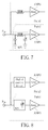
- FIG. 7 illustrates some implementation details of the apparatus 100 shown in FIG. 1 according to another embodiment of the present invention, where the signal path Path1 can be taken as an example of the first path, and the signal path Path2 can be taken as an example of the second path.
- the capacitor electrically connected between the input port P in and the amplifier AMP2 has been replaced by an inductor.
- similar descriptions for this embodiment are not repeated in detail here.
- FIG. 8 illustrates some implementation details of the apparatus 100 shown in FIG. 1 according to another embodiment of the present invention, where the signal path Path1 can be taken as an example of the first path, and the signal path Path2 can be taken as an example of the second path.
- the capacitor electrically connected between the input port P in and the amplifier AMP2 has been replaced by a high-impedance device (labeled "High Z passive device" in FIG. 8 , for better comprehension).
- High Z passive device labeled "High Z passive device” in FIG. 8 , for better comprehension
Landscapes
- Engineering & Computer Science (AREA)
- Power Engineering (AREA)
- Computer Networks & Wireless Communication (AREA)
- Signal Processing (AREA)
- Amplifiers (AREA)
Description
- The present invention relates to a matching network circuit and an associated apparatus according to the pre-characterizing clauses of
claims 1 and 11. - According to the related art, conventional impedance matching networks may be utilized for performing impedance matching in a conventional portable electronic device, to resolve some transmission issues. However, further problems such as some side effects may occur. For example, each of the conventional impedance matching networks typically occupies a large portion of the chip area. In another example, in a situation where two of the conventional impedance matching networks are positioned on two signal paths that are related to each other, re-designing the two of the conventional impedance matching networks may be required since one conventional impedance matching network of them may affect the other conventional impedance matching network. Thus, how to improve impedance matching control of electronic devices in order to guarantee the overall performance of the electronic devices with fewer side effects has become an important issue to be solved.
- This in mind, the present invention aims at providing a matching network circuit and an associated apparatus that reduce the chip area of a semiconductor chip and/or keep high stability of an electronic device in each of various situations.
- This is achieved by a matching network circuit and an associated apparatus according to the pre-characterizing clauses of
claims 1 and 11. The dependent claims pertain to corresponding further developments and improvements. - In one aspect, the disclosure features a matching network circuit, where the matching network circuit may comprise a matching unit that is coupled between a common path port and a first path port of the matching network circuit, and may further comprise an impedance unit that is coupled between the common path port and a second path port of the matching network circuit. In addition, the common path port is utilized for connecting the matching network circuit to a common path, the first path port is utilized for connecting the matching network circuit to a first device on a first path, and the second path port is utilized for connecting the matching network circuit to a second device on a second path, wherein signals on the first and the second paths have a same transmission direction (e.g. an input direction, or an output direction) with respect to a node between the common path and the first and the second paths. Additionally, the matching unit may be arranged for performing impedance matching between the common path port and the first path port, and the impedance unit may be arranged for performing impedance matching between the common path port and the second path port with aid of the matching unit. In some embodiments, there is not any switch between the common path port and the impedance unit, and there is not any switch between the second path port and the impedance unit, where there is not any switch between the second path port and the second device. In some embodiments, there is not any switch between the common path port and the matching unit, and there is not any switch between the first path port and the matching unit, where there is not any switch between the first path port and the first device. For example, both of the first path port and the second path port are input ports. In another example, both of the first path port and the second path port are output ports.
- In one aspect, the disclosure features an associated apparatus, where the apparatus may comprise a first device on a first path, a second device on a second path, and a matching network circuit that is coupled between the first device and the second device. For example, the matching network circuit may comprise a matching unit that is coupled between a common path port and a first path port of the matching network circuit, and may further comprise an impedance unit that is coupled between the common path port and a second path port of the matching network circuit. In addition, the common path port is utilized for connecting the matching network circuit to a common path, the first path port is utilized for connecting the matching network circuit to the first device on the first path, and the second path port is utilized for connecting the matching network circuit to the second device on the second path, wherein signals on the first and the second paths have a same transmission direction (e.g. an input direction, or an output direction) with respect to a node between the common path and the first and the second paths. Additionally, the matching unit may be arranged for performing impedance matching between the common path port and the first path port, and the impedance unit may be arranged for performing impedance matching between the common path port and the second path port with aid of the matching unit, where the first device and the second device share the matching network circuit. In some embodiments, there is not any switch between the common path port and the impedance unit, and there is not any switch between the second path port and the impedance unit, where there is not any switch between the second path port and the second device. In some embodiments, there is not any switch between the common path port and the matching unit, and there is not any switch between the first path port and the matching unit, where there is not any switch between the first path port and the first device. For example, both of the first path port and the second path port are input ports. In another example, both of the first path port and the second path port are output ports.
- It is an advantage of the present invention that the present invention circuit and apparatus can keep high stability of the electronic device in each of various situations, and the related art problems will no longer be an issue. In addition, the present invention circuit and apparatus can reduce the chip area of a semiconductor chip of the electronic device.
- In the following, the invention is further illustrated by way of example, taking reference to the accompanying drawings. Thereof
- FIG. 1
- is a diagram of an apparatus with a shared matching network circuit according to an embodiment of the present invention,
- FIG. 2
- illustrates some implementation details of the apparatus shown in
FIG. 1 according to an embodiment of the present invention, - FIG. 3
- illustrates some implementation details of the apparatus shown in
FIG. 1 according to another embodiment of the present invention, - FIG. 4
- illustrates some implementation details of the apparatus shown in
FIG. 1 according to another embodiment of the present invention, - FIG. 5
- illustrates some implementation details of the apparatus shown in
FIG. 1 according to another embodiment of the present invention, - FIG. 6
- illustrates some implementation details of the apparatus shown in
FIG. 1 according to another embodiment of the present invention, - FIG. 7
- illustrates some implementation details of the apparatus shown in
FIG. 1 according to another embodiment of the present invention, and - FIG. 8
- illustrates some implementation details of the apparatus shown in
FIG. 1 according to another embodiment of the present invention. - Certain terms are used throughout the following description and claims, which refer to particular components. As one skilled in the art will appreciate, electronic equipment manufacturers may refer to a component by different names. This document does not intend to distinguish between components that differ in name but not in function. In the following description and in the claims, the terms "include" and "comprise" are used in an open-ended fashion, and thus should be interpreted to mean "include, but not limited to ...". Also, the term "couple" is intended to mean either an indirect or direct electrical connection. Accordingly, if one device is coupled to another device, that connection may be through a direct electrical connection, or through an indirect electrical connection via other devices and connections.
-
FIG. 1 is a diagram of anapparatus 100 with a shared matching network circuit according to an embodiment of the present invention, where theapparatus 100 may comprise at least one portion (e.g. a portion or all) of an electronic device. For example, theapparatus 100 may comprise a portion of the electronic device mentioned above, and more particularly, can be at least one hardware circuit such as at least one integrated circuit (IC) within the electronic device and associated circuits thereof. In another example, theapparatus 100 can be the whole of the electronic device mentioned above. In another example, theapparatus 100 may comprise a system comprising the electronic device mentioned above (e.g. a wireless communications system comprising the electronic device). Examples of the electronic device may include, but not limited to, a mobile phone (e.g. a multifunctional mobile phone), a tablet, and a personal computer such as a laptop computer or a desktop computer. - As shown in
FIG. 1 , theapparatus 100 may comprise a first device 51 (labeled "Device(1)" inFIG. 1 , for better comprehension) on a first path within the electronic device, a second device 52 (labeled "Device(2)" inFIG. 1 , for better comprehension) on a second path within the electronic device, and amatching network circuit 110 that is coupled between thefirst device 51 and thesecond device 52, where all of thefirst device 51, thesecond device 52, and thematching network circuit 110 are positioned in the electronic device. For example, thematching network circuit 110 may comprise amatching unit 111 that is coupled between a common path port Pcom and a first path port P1 of thematching network circuit 110, and may further comprise animpedance unit 112 that is coupled between the common path port Pcom and a second path port P2 of thematching network circuit 110, where the matchingunit 111 may be positioned on the first path, and theimpedance unit 112 may be positioned on the second path. In addition, the common path port Pcom is utilized for connecting thematching network circuit 110 to a common path, the first path port P1 is utilized for connecting thematching network circuit 110 to thefirst device 51 on the first path, and the second path port P2 is utilized for connecting thematching network circuit 110 to thesecond device 52 on the second path, where signals on the first and the second paths have the same transmission direction (e.g. an input direction, or an output direction) with respect to a node between the common path and the first and the second paths. Additionally, the matchingunit 111 may be arranged for performing impedance matching between the common path port Pcom and the first path port P1, and theimpedance unit 112 may be arranged for performing impedance matching between the common path port Pcom and the second path port P2 with aid of the matchingunit 111. Please note that thefirst device 51 on the first path and thesecond device 52 on the second path share thematching network circuit 110. Therefore, only one matching unit (e.g. the matching unit 111) is needed. This is for illustrative purposes only, and is not meant to be a limitation of the present invention. According to some embodiments, the combination of the matchingunit 111 and theimpedance unit 112 can be utilized for performing impedance matching for thesecond device 52 on the second path, and the matchingunit 111 can be utilized for performing impedance matching for thefirst device 51 on the first path, where the existence of theimpedance unit 112 does not hinder the impedance matching that the matchingunit 111 performs for thefirst device 51 on the first path. In some embodiments, whether theimpedance unit 112 exists or not does not significantly affect the impedance matching that thematching unit 111 performs for thefirst device 51 on the first path. In some embodiments, regarding the impedance matching that the matchingunit 111 performs for thefirst device 51 on the first path, there is no significant difference between installing theimpedance unit 112 and not installing theimpedance unit 112. - According to this embodiment, there is not any switch between the common path port Pcom and the
matching unit 111, and there is not any switch between the first path port P1 and thematching unit 111, where there is not any switch between the first path port P1 and thefirst device 51. In addition, there is not any switch between the common path port Pcom and theimpedance unit 112, and there is not any switch between the second path port P2 and theimpedance unit 112, where there is not any switch between the second path port P2 and thesecond device 52. For example, each of thefirst device 51 and thesecond device 52 can be an amplifier (e.g. a power amplifier, or a low noise amplifier (LNA)), or can be one of other types of circuits such as other devices or components. - According to some embodiments, the impedance of the
impedance unit 112 is higher than that of thematching unit 111 so that thematching unit 111 dominates the overall impedance of the matching network circuit 110 (e.g., on the first path). For example, the impedance of thematching unit 111 and the impedance of theimpedance unit 112 may differ by one or more orders, so the impedance of theimpedance unit 112 may be one or more orders of magnitude greater than that of thematching unit 111. More particularly, the impedance of theimpedance unit 112 may be multiple orders of magnitude greater than that of thematching unit 111. In some embodiments, the impedance of thematching unit 111 may be approximately 50 Ohm (Ω), while the impedance of theimpedance unit 112 may be much greater than that of thematching unit 111. - According to some embodiments, the
matching unit 111 may comprise a capacitor bank. For example, the capacitor bank may be tunable. More particularly, the capacitor bank may be used for fine tuning the overall impedance of thematching network circuit 110. According to some embodiments, theimpedance unit 112 may comprise a passive component (e.g. a capacitor, an inductor, or a high-impedance device). For example, theimpedance unit 112 may be the passive component, and there is not any other component within theimpedance unit 112. This is for illustrative purposes only, and is not meant to be a limitation of the present invention. According to some embodiments of the present invention, theimpedance unit 112 may comprise one or more passive components. Examples of the aforementioned one or more passive components may include, but not limited to, capacitors, inductors, and high-impedance devices. - In some embodiments, the signals on the first and the second paths may have the same transmission direction with respect to the node between the common path and the first and the second paths, such as the aforementioned output direction, and the signals on the first and the second paths are output signals from this node. Thus, both of the first path port P1 and the second path port P2 may be output ports of the
matching network circuit 110. In this situation, the common path port Pcom is an input port Pin of thematching network circuit 110. For example, thematching network circuit 110 may receive an input signal at the input port Pin, and thematching network circuit 110 may be coupled to an input terminal of thefirst device 51 through the first path port P1, and may be coupled to an input terminal of thesecond device 52 through the second path port P2. More particularly, thematching network circuit 110 may filter the input signal to generate a first intermediate signal on the first path and to generate a second intermediate signal on the second path, where the input terminal of thefirst device 51 may input the first intermediate signal into thefirst device 51, and the input terminal of thesecond device 52 may input the second intermediate signal into thesecond device 52. For example, thefirst device 51, thesecond device 52, and thematching network circuit 110 may be positioned in a transmitter within the electronic device, and each of thefirst device 51 and thesecond device 52 can be the power amplifier mentioned above. - In some embodiments, the signals on the first and the second paths may have the same transmission direction with respect to the node between the common path and the first and the second paths, such as the aforementioned input direction, and the signals on the first and the second paths are input signals into this node. Thus, both of the first path port P1 and the second path port P2 may be input ports of the
matching network circuit 110. In this situation, the common path port Pcom is an output port Pout of thematching network circuit 110. For example, thematching network circuit 110 may output an output signal at the output port Pout, and thematching network circuit 110 may be coupled to an output terminal of thefirst device 51 through the first path port P1, and may be coupled to an output terminal of thesecond device 52 through the second path port P2. More particularly, thematching network circuit 110 may filter a first intermediate signal on the first path and a second intermediate signal on the second path to generate the output signal, where the output terminal of thefirst device 51 may output the first intermediate signal from thefirst device 51, and the output terminal of thesecond device 52 may output the second intermediate signal from thesecond device 52. For example, thefirst device 51, thesecond device 52, and thematching network circuit 110 may be positioned in a receiver within the electronic device, and each of thefirst device 51 and thesecond device 52 can be the LNA mentioned above. -
FIG. 2 illustrates some implementation details of theapparatus 100 shown inFIG. 1 according to an embodiment of the present invention, where the input port Pin can be taken as an example of the input port Pin mentioned above. For example, thefirst device 51 and thesecond device 52 can be implemented with two amplifiers AMP1 and AMP2 (each of which is labeled "Amp" inFIG. 2 , for brevity), respectively, and the two amplifiers AMP1 and AMP2 can be power amplifiers positioned in a transmitter such as that mentioned above, and can be single-ended amplifiers. In addition, the matching network (MN) can be taken as an example of thematching unit 111 shown inFIG. 1 , and may comprise the aforementioned capacitor bank that may be tunable. Additionally, the capacitor electrically connected between the input port Pin and the amplifier AMP2 can be taken as an example of the aforementioned passive component within theimpedance unit 112. Based on the architecture shown inFIG. 2 , the first path port P1 of this embodiment comprises a single output terminal electrically connected to the input terminal of the amplifier AMP1, and the second path port P2 of this embodiment comprises a single output terminal electrically connected to the input terminal of the amplifier AMP2. For brevity, similar descriptions for this embodiment are not repeated in detail here. - In the embodiment shown in
FIG. 2 , the capacitor electrically connected between the input port Pin and the amplifier AMP2 can be taken as an example of the aforementioned passive component within theimpedance unit 112. This is for illustrative purposes only, and is not meant to be a limitation of the present invention. According to some embodiments of the present invention, the passive component may vary. For example, this capacitor may be replaced by an inductor. In another example, this capacitor may be replaced by a high-impedance device. -
FIG. 3 illustrates some implementation details of theapparatus 100 shown inFIG. 1 according to another embodiment of the present invention, where the input port Pin can be taken as an example of the input port Pin mentioned above. For example, thefirst device 51 and thesecond device 52 can be implemented with a differential amplifier DF_AMP and a single-ended amplifier SE_AMP (each of which is labeled "Amp" inFIG. 3 , for brevity), respectively, and the differential amplifier DF_AMP and the single-ended amplifier SE_AMP can be power amplifiers positioned in a transmitter such as that mentioned above. In addition, thematching unit 111 of this embodiment may comprise a balun and a tunable capacitor bank (e.g. the aforementioned capacitor bank that may be tunable). Additionally, the capacitor electrically connected between the input port Pin and the single-ended amplifier SE_AMP can be taken as an example of the aforementioned passive component within theimpedance unit 112. Based on the architecture shown inFIG. 3 , the first path port P1 of this embodiment comprises two differential output terminals electrically connected to the two differential input terminals of the differential amplifier DF_AMP, and the second path port P2 of this embodiment comprises a single output terminal electrically connected to the input terminal of the single-ended amplifier SE_AMP. For brevity, similar descriptions for this embodiment are not repeated in detail here. - In the embodiment shown in
FIG. 3 , the capacitor electrically connected between the input port Pin and the single-ended amplifier SE_AMP can be taken as an example of the aforementioned passive component within theimpedance unit 112. This is for illustrative purposes only, and is not meant to be a limitation of the present invention. According to some embodiments of the present invention, the passive component may vary. For example, this capacitor may be replaced by an inductor. In another example, this capacitor may be replaced by a high-impedance device. - According to some embodiments, the input impedance of the second device 52 (e.g. the amplifier AMP2, or the single-ended amplifier SE_AMP) should be much higher than 50 Ohm, and the
input matching unit 111 has matched the first device 51 (e.g. the amplifier AMP1, or the differential amplifier DF_AMP) to the impedance of 50 Ohm. After thesecond device 52 is connected through theimpedance unit 112 to thematching unit 111, the impedance at the common path port Pcom (e.g. the input port Pin) is still close to 50 Ohm. For example, in a situation where the common path port Pcom is the input port Pin of thematching network circuit 110, thematching unit 111 can be regarded as the input matching unit for thefirst device 51. In this situation, after thesecond device 52 is connected through theimpedance unit 112 to the input matching unit for thefirst device 51, such as thematching unit 111, the input impedance at the input port Pin is still close to 50 Ohm. - According to some embodiments, the
impedance unit 112 can be regarded as the input or output matching for the second device 52 (e.g. the amplifier AMP2, or the single-ended amplifier SE_AMP). For example, theimpedance unit 112 can be reduced to one series capacitor (e.g. for direct current (DC) blocking) after thesecond device 52 is coupled through thematching network circuit 110 to the first device 51 (e.g. the amplifier AMP1, or the differential amplifier DF_AMP). - According to some embodiments, no switch is needed in between the second device 52 (e.g. the amplifier AMP2, or the single-ended amplifier SE_AMP) and the first device 51 (e.g. the amplifier AMP1, or the differential amplifier DF_AMP), where the
first device 51 and thesecond device 52 may operate independently. For example, thefirst device 51 and thesecond device 52 may operate independently while keeping similar input return loss. Please note that, in conventional dual paths matching, it is hard to implement shared matching network for both amplifiers but still keep the same matching impedance since the matching impedance would be variant during switching between turning on and turning off the amplifiers. Based on the architecture in any of the above embodiments of the present invention, the present invention circuit and apparatus (e.g. thematching network circuit 110 and the apparatus 100) can keep high stability of the electronic device in each of various situations, and the related art problems will no longer be an issue. -
FIG. 4 illustrates some implementation details of theapparatus 100 shown inFIG. 1 according to another embodiment of the present invention, where the output port Pout can be taken as an example of the output port Pout mentioned above. For example, thefirst device 51 and thesecond device 52 can be implemented with two amplifiers AMP1 and AMP2 (each of which is labeled "Amp" inFIG. 4 , for brevity), respectively, and the two amplifiers AMP1 and AMP2 can be power amplifiers positioned in a transmitter such as that mentioned above, and can be single-ended amplifiers. In addition, the matching network (MN) can be taken as an example of thematching unit 111 shown inFIG. 1 , and may comprise the aforementioned capacitor bank that may be tunable. Additionally, the capacitor electrically connected between the output port Pout and the amplifier AMP2 can be taken as an example of the aforementioned passive component within theimpedance unit 112. Based on the architecture shown inFIG. 4 , the first path port P1 of this embodiment comprises a single input terminal electrically connected to the output terminal of the amplifier AMP1, and the second path port P2 of this embodiment comprises a single input terminal electrically connected to the output terminal of the amplifier AMP2. For brevity, similar descriptions for this embodiment are not repeated in detail here. - In the embodiment shown in
FIG. 4 , the capacitor electrically connected between the output port Pout and the amplifier AMP2 can be taken as an example of the aforementioned passive component within theimpedance unit 112. This is for illustrative purposes only, and is not meant to be a limitation of the present invention. According to some embodiments of the present invention, the passive component may vary. For example, this capacitor may be replaced by an inductor. In another example, this capacitor may be replaced by a high-impedance device. -
FIG. 5 illustrates some implementation details of theapparatus 100 shown inFIG. 1 according to another embodiment of the present invention, where the input port Pin can be taken as an example of the input port Pin mentioned above. For example, thefirst device 51 can be implemented with the amplifier AMP(1) (labeled "Amp" inFIG. 5 , for brevity) such as the amplifier AMP1 shown inFIG. 2 , and thesecond device 52 can be implemented with one of the amplifiers AMP(2), ..., and AMP(n) (labeled "Amp" inFIG. 5 , for brevity), such as the amplifier AMP2 shown inFIG. 2 . Thus, thesecond device 52 may be extended to a set of second devices. In the architecture shown inFIG. 5 , the amplifiers AMP(1), AMP(2), ..., and AMP(n) can be power amplifiers positioned in a transmitter such as that mentioned above, and can be single-ended amplifiers. This is for illustrative purposes only, and is not meant to be a limitation of the present invention. According to some embodiments, the amplifier AMP(1) may be replaced by a differential amplifier such as the differential amplifier DF_AMP shown inFIG. 3 . According to some embodiments, in a situation where the input and output directions of each of the amplifiers AMP(1), AMP(2), ..., and AMP(n) shown inFIG. 5 are reversed, the amplifiers AMP(1), AMP(2), ..., and AMP(n) of these embodiments can be LNAs positioned in a receiver such as that mentioned above, and can be single-ended amplifiers. According to some embodiments, in a situation where the input and output directions of each of the amplifiers AMP(1), AMP(2), ..., and AMP(n) shown inFIG. 5 are reversed, the amplifiers AMP(1), AMP(2), ..., and AMP(n) of these embodiments can be LNAs positioned in a receiver such as that mentioned above, where the amplifier AMP(1) may be replaced by a differential amplifier such as the differential amplifier DF_AMP shown inFIG. 3 , and the other amplifiers within the amplifiers AMP(1), AMP(2), ..., and AMP(n) of these embodiments can be single-ended amplifiers. - In addition, the matching network (MN) can be taken as an example of the
matching unit 111 shown inFIG. 1 , and may comprise the aforementioned capacitor bank that may be tunable. Additionally, the capacitor electrically connected between the input port Pin and one of the amplifiers AMP(2), ..., and AMP(n) can be taken as an example of the aforementioned passive component within theimpedance unit 112. Based on the architecture shown inFIG. 5 , the first path port P1 of this embodiment comprises a single output terminal electrically connected to the input terminal of the amplifier AMP(1), and the second path port P2 of this embodiment has been extended to be a set of second path ports {P2}, each of which comprises a single output terminal electrically connected to the input terminal of one of the amplifiers AMP(2), ..., and AMP(n). For brevity, similar descriptions for this embodiment are not repeated in detail here. - In the embodiment shown in
FIG. 5 , the capacitor electrically connected between the input port Pin and one of the amplifiers AMP(2), ..., and AMP(n) can be taken as an example of the aforementioned passive component within theimpedance unit 112. This is for illustrative purposes only, and is not meant to be a limitation of the present invention. According to some embodiments of the present invention, the passive component may vary. For example, this capacitor may be replaced by an inductor. In another example, this capacitor may be replaced by a high-impedance device. -
FIG. 6 illustrates some implementation details of theapparatus 100 shown inFIG. 1 according to another embodiment of the present invention, where the signal path Path1 can be taken as an example of the first path, and the signal path Path2 can be taken as an example of the second path. In comparison with the embodiment shown inFIG. 2 , the architecture of the matching network (MN) may become more complicated when needed. In addition to the aforementioned capacitor bank that may be tunable, the matching network (MN) of this embodiment may further comprise an additional capacitor and an inductor coupled between the capacitor bank and the additional capacitor. For brevity, similar descriptions for this embodiment are not repeated in detail here. -
FIG. 7 illustrates some implementation details of theapparatus 100 shown inFIG. 1 according to another embodiment of the present invention, where the signal path Path1 can be taken as an example of the first path, and the signal path Path2 can be taken as an example of the second path. In comparison with the embodiment shown inFIG. 6 , the capacitor electrically connected between the input port Pin and the amplifier AMP2 has been replaced by an inductor. For brevity, similar descriptions for this embodiment are not repeated in detail here. -
FIG. 8 illustrates some implementation details of theapparatus 100 shown inFIG. 1 according to another embodiment of the present invention, where the signal path Path1 can be taken as an example of the first path, and the signal path Path2 can be taken as an example of the second path. In comparison with the embodiment shown inFIG. 2 , the capacitor electrically connected between the input port Pin and the amplifier AMP2 has been replaced by a high-impedance device (labeled "High Z passive device" inFIG. 8 , for better comprehension). For brevity, similar descriptions for this embodiment are not repeated in detail here. - All combinations and sub-combinations of above-described features also belong to the invention.
Claims (15)
- A matching network circuit (110), characterized in that the matching network circuit comprises:a matching unit (111, MN), coupled between a common path port (Pcom, Pin, Pout) and a first path port (P1) of the matching network circuit (110), arranged for performing impedance matching between the common path port (Pcom, Pin, Pout) and the first path port (P1), wherein the common path port (Pcom, Pin, Pout) is utilized for connecting the matching network circuit (110) to a common path, and the first path port (P1) is utilized for connecting the matching network circuit (110) to a first device (51, DF_AMP, AMP1, AMP(1)) on a first path; andan impedance unit (112), coupled between the common path port (Pcom, Pin, Pout) and a second path port (P2) of the matching network circuit (110), arranged for performing impedance matching between the common path port (Pcom, Pin, Pout) and the second path port (P2) with aid of the matching unit (111, MN), wherein the second path port (P2) is utilized for connecting the matching network circuit (110) to a second device (52, SE_AMP, AMP2, AMP(2), ..., AMP(n)) on a second path, and signals on the first and the second paths have a same transmission direction with respect to a node between the common path and the first and the second paths.
- The matching network circuit of claim 1, characterized in that an impedance of the impedance unit (112) is higher than that of the matching unit (111, MN) so that the matching unit (111, MN) dominates an overall impedance of the matching network circuit (110).
- The matching network circuit of claim 1, characterized in that the matching unit (111, MN) comprises:a capacitor bank.
- The matching network circuit of claim 3, characterized in that the capacitor bank is tunable.
- The matching network circuit of claim 4, characterized in that the capacitor bank is used for fine tuning an overall impedance of the matching network circuit (110).
- The matching network circuit of claim 1, characterized in that the impedance unit (112) comprises:a passive component.
- The matching network circuit of claim 1, characterized in that there is not any switch between the common path port (Pcom, Pin, Pout) and the impedance unit (112), and there is not any switch between the second path port (P2) and the impedance unit (112), wherein there is not any switch between the second path port (P2) and the second device (52, SE_AMP, AMP2, AMP(2), ..., AMP(n)).
- The matching network circuit of claim 1, characterized in that there is not any switch between the common path port (Pcom, Pin, Pout) and the matching unit (111, MN), and there is not any switch between the first path port (P1) and the matching unit (111, MN), wherein there is not any switch between the first path port (P1) and the first device (51, DF_AMP, AMP1, AMP(1)).
- The matching network circuit of claim 1, characterized in that both of the first path port (P1) and the second path port (P2) are input ports.
- The matching network circuit of claim 1, characterized in that both of the first path port (P1) and the second path port (P2) are output ports.
- An apparatus (100), characterized in that the apparatus comprises the matching network circuit (110) of claim 1 and further comprises the first device (51, DF_AMP, AMP1, AMP(1)) and the second device (52, SE_AMP, AMP2, AMP(2), ..., AMP(n)), wherein the matching network circuit (110) is coupled between the first device (51, DF_AMP, AMP1, AMP(1)) and the second device (52, SE_AMP, AMP2, AMP(2), ..., AMP(n)), and the first device (51, DF_AMP, AMP1, AMP(1)) and the second device (52, SE_AMP, AMP2, AMP(2), ..., AMP(n)) share the matching network circuit (110).
- The apparatus of claim 11, characterized in that the matching network circuit (110) receives an input signal and is coupled to an input terminal of the first device (51, DF_AMP, AMP1, AMP(1)) and an input terminal of the second device (52, SE_AMP, AMP2, AMP(2), ..., AMP(n)).
- The apparatus of claim 12, characterized in that the matching network circuit (110) filters the input signal to generate a first intermediate signal on the first path and to generate a second intermediate signal on the second path, wherein the input terminal of the first device (51, DF_AMP, AMP1, AMP(1)) inputs the first intermediate signal into the first device (51, DF_AMP, AMP1, AMP(1)), and the input terminal of the second device (52, SE_AMP, AMP2, AMP(2), ..., AMP(n)) inputs the second intermediate signal into the second device (52, SE_AMP, AMP2, AMP(2), ..., AMP(n)).
- The apparatus of claim 11, characterized in that the matching network circuit (110) outputs an output signal and is coupled to an output terminal of the first device (51, DF_AMP, AMP1, AMP(1)) and an output terminal of the second device (52, SE_AMP, AMP2, AMP(2), ..., AMP(n)).
- The apparatus of claim 14, characterized in that the matching network circuit (110) filters a first intermediate signal on the first path and a second intermediate signal on the second path to generate the output signal, wherein the output terminal of the first device (51, DF_AMP, AMP1, AMP(1)) outputs the first intermediate signal from the first device (51, DF_AMP, AMP1, AMP(1)), and the output terminal of the second device (52, SE_AMP, AMP2, AMP(2), ..., AMP(n)) outputs the second intermediate signal from the second device (52, SE_AMP, AMP2, AMP(2), ..., AMP(n)).
Applications Claiming Priority (2)
| Application Number | Priority Date | Filing Date | Title |
|---|---|---|---|
| US201562244711P | 2015-10-21 | 2015-10-21 | |
| US15/201,501 US10382004B2 (en) | 2015-10-21 | 2016-07-03 | Matching network circuit, and associated apparatus with shared matching network circuit |
Publications (2)
| Publication Number | Publication Date |
|---|---|
| EP3160046A1 true EP3160046A1 (en) | 2017-04-26 |
| EP3160046B1 EP3160046B1 (en) | 2019-02-27 |
Family
ID=56681934
Family Applications (1)
| Application Number | Title | Priority Date | Filing Date |
|---|---|---|---|
| EP16178377.4A Active EP3160046B1 (en) | 2015-10-21 | 2016-07-07 | Matching network circuit, and associated apparatus with shared matching network circuit |
Country Status (3)
| Country | Link |
|---|---|
| US (1) | US10382004B2 (en) |
| EP (1) | EP3160046B1 (en) |
| CN (1) | CN106612108B (en) |
Citations (4)
| Publication number | Priority date | Publication date | Assignee | Title |
|---|---|---|---|---|
| US20060030282A1 (en) * | 2001-11-14 | 2006-02-09 | Sudhir Aggarwal | Impedance matching circuit for a multi-band radio frequency device |
| US20080136516A1 (en) * | 2006-12-06 | 2008-06-12 | Broadcom Corporation, A California Corporation | RFIC with high power PA |
| US20130234799A1 (en) * | 2012-03-07 | 2013-09-12 | Qualcomm Incorporated | Shared bypass capacitor matching network |
| US20140179241A1 (en) * | 2012-12-20 | 2014-06-26 | Qualcomm Incorporated | Concurrent matching network using transmission lines for low loss |
Family Cites Families (7)
| Publication number | Priority date | Publication date | Assignee | Title |
|---|---|---|---|---|
| US6188877B1 (en) | 1997-07-03 | 2001-02-13 | Ericsson Inc. | Dual-band, dual-mode power amplifier with reduced power loss |
| US5969582A (en) | 1997-07-03 | 1999-10-19 | Ericsson Inc. | Impedance matching circuit for power amplifier |
| US8417201B1 (en) | 2009-06-24 | 2013-04-09 | Rf Micro Devices, Inc. | Dual path multi-mode power amplifier routing architecture |
| US8611834B2 (en) * | 2010-11-01 | 2013-12-17 | Cree, Inc. | Matching network for transmission circuitry |
| US9031517B2 (en) | 2011-09-28 | 2015-05-12 | Mediatek | Transmit-receive front end |
| US9419568B2 (en) | 2013-06-03 | 2016-08-16 | Skyworks Solutions, Inc. | Circuits and methods related to power amplifier efficiency based on multi-harmonic approximation |
| TWI544754B (en) * | 2014-01-28 | 2016-08-01 | A wireless transceiver device with frequency band matching adjustment function and its adjustment method |
-
2016
- 2016-07-03 US US15/201,501 patent/US10382004B2/en active Active
- 2016-07-07 EP EP16178377.4A patent/EP3160046B1/en active Active
- 2016-08-30 CN CN201610765771.9A patent/CN106612108B/en active Active
Patent Citations (4)
| Publication number | Priority date | Publication date | Assignee | Title |
|---|---|---|---|---|
| US20060030282A1 (en) * | 2001-11-14 | 2006-02-09 | Sudhir Aggarwal | Impedance matching circuit for a multi-band radio frequency device |
| US20080136516A1 (en) * | 2006-12-06 | 2008-06-12 | Broadcom Corporation, A California Corporation | RFIC with high power PA |
| US20130234799A1 (en) * | 2012-03-07 | 2013-09-12 | Qualcomm Incorporated | Shared bypass capacitor matching network |
| US20140179241A1 (en) * | 2012-12-20 | 2014-06-26 | Qualcomm Incorporated | Concurrent matching network using transmission lines for low loss |
Also Published As
| Publication number | Publication date |
|---|---|
| CN106612108B (en) | 2019-06-14 |
| CN106612108A (en) | 2017-05-03 |
| EP3160046B1 (en) | 2019-02-27 |
| US20170117870A1 (en) | 2017-04-27 |
| US10382004B2 (en) | 2019-08-13 |
Similar Documents
| Publication | Publication Date | Title |
|---|---|---|
| US10879942B2 (en) | Demultiplexing apparatus and method of designing the apparatus | |
| CN108292793B (en) | Electromagnetic coupler for multi-frequency power detection | |
| EP3166224B1 (en) | Frequency tunable filter with voltage stressed relaxed switch, and associated apparatus | |
| US7795966B2 (en) | Balanced amplifier with protection circuit | |
| US10742189B2 (en) | Switched multi-coupler apparatus and modules and devices using same | |
| KR20170093208A (en) | Adjustable rf coupler | |
| JP2004015307A (en) | Variable antenna matching circuit | |
| US10340959B2 (en) | Front-end module and communication device | |
| US5778306A (en) | Low loss high frequency transmitting/receiving switching module | |
| US9136991B2 (en) | Power amplifying circuit and front end module including the same | |
| WO2014020297A1 (en) | Radio frequency transceivers | |
| WO2016086978A1 (en) | Quadrature signal generator, beamforming arrangement, communication device and base station | |
| US10199709B2 (en) | Microwave power combiner | |
| CN108141179A (en) | Power amplifier | |
| US12323114B2 (en) | Biasing solution for push-pull power amplifier for low loadline and high common mode rejection ratio background | |
| EP3160046B1 (en) | Matching network circuit, and associated apparatus with shared matching network circuit | |
| TWI729823B (en) | Wireless communication circuits and associated wireless communication devices | |
| WO2014159172A1 (en) | Passive radio frequency signal handler | |
| CN113746445A (en) | Directional coupler | |
| TW201517379A (en) | Antenna tuner | |
| US20240332778A1 (en) | Directional coupler, radio frequency module, and communication apparatus | |
| EP4222872B1 (en) | A transceiver switch circuitry | |
| CN121308689A (en) | RF power amplifier and RF front-end module | |
| KR101034097B1 (en) | SAS Duplexer Module Using Inverter | |
| KR20130113239A (en) | Circuit for matching impedence |
Legal Events
| Date | Code | Title | Description |
|---|---|---|---|
| PUAI | Public reference made under article 153(3) epc to a published international application that has entered the european phase |
Free format text: ORIGINAL CODE: 0009012 |
|
| STAA | Information on the status of an ep patent application or granted ep patent |
Free format text: STATUS: THE APPLICATION HAS BEEN PUBLISHED |
|
| AK | Designated contracting states |
Kind code of ref document: A1 Designated state(s): AL AT BE BG CH CY CZ DE DK EE ES FI FR GB GR HR HU IE IS IT LI LT LU LV MC MK MT NL NO PL PT RO RS SE SI SK SM TR |
|
| AX | Request for extension of the european patent |
Extension state: BA ME |
|
| STAA | Information on the status of an ep patent application or granted ep patent |
Free format text: STATUS: REQUEST FOR EXAMINATION WAS MADE |
|
| 17P | Request for examination filed |
Effective date: 20170720 |
|
| RBV | Designated contracting states (corrected) |
Designated state(s): AL AT BE BG CH CY CZ DE DK EE ES FI FR GB GR HR HU IE IS IT LI LT LU LV MC MK MT NL NO PL PT RO RS SE SI SK SM TR |
|
| GRAP | Despatch of communication of intention to grant a patent |
Free format text: ORIGINAL CODE: EPIDOSNIGR1 |
|
| STAA | Information on the status of an ep patent application or granted ep patent |
Free format text: STATUS: GRANT OF PATENT IS INTENDED |
|
| INTG | Intention to grant announced |
Effective date: 20181122 |
|
| GRAS | Grant fee paid |
Free format text: ORIGINAL CODE: EPIDOSNIGR3 |
|
| GRAA | (expected) grant |
Free format text: ORIGINAL CODE: 0009210 |
|
| STAA | Information on the status of an ep patent application or granted ep patent |
Free format text: STATUS: THE PATENT HAS BEEN GRANTED |
|
| AK | Designated contracting states |
Kind code of ref document: B1 Designated state(s): AL AT BE BG CH CY CZ DE DK EE ES FI FR GB GR HR HU IE IS IT LI LT LU LV MC MK MT NL NO PL PT RO RS SE SI SK SM TR |
|
| REG | Reference to a national code |
Ref country code: GB Ref legal event code: FG4D |
|
| REG | Reference to a national code |
Ref country code: CH Ref legal event code: EP |
|
| REG | Reference to a national code |
Ref country code: AT Ref legal event code: REF Ref document number: 1102807 Country of ref document: AT Kind code of ref document: T Effective date: 20190315 |
|
| REG | Reference to a national code |
Ref country code: IE Ref legal event code: FG4D |
|
| REG | Reference to a national code |
Ref country code: DE Ref legal event code: R096 Ref document number: 602016010264 Country of ref document: DE |
|
| REG | Reference to a national code |
Ref country code: NL Ref legal event code: MP Effective date: 20190227 |
|
| REG | Reference to a national code |
Ref country code: LT Ref legal event code: MG4D |
|
| PG25 | Lapsed in a contracting state [announced via postgrant information from national office to epo] |
Ref country code: PT Free format text: LAPSE BECAUSE OF FAILURE TO SUBMIT A TRANSLATION OF THE DESCRIPTION OR TO PAY THE FEE WITHIN THE PRESCRIBED TIME-LIMIT Effective date: 20190627 Ref country code: SE Free format text: LAPSE BECAUSE OF FAILURE TO SUBMIT A TRANSLATION OF THE DESCRIPTION OR TO PAY THE FEE WITHIN THE PRESCRIBED TIME-LIMIT Effective date: 20190227 Ref country code: FI Free format text: LAPSE BECAUSE OF FAILURE TO SUBMIT A TRANSLATION OF THE DESCRIPTION OR TO PAY THE FEE WITHIN THE PRESCRIBED TIME-LIMIT Effective date: 20190227 Ref country code: NO Free format text: LAPSE BECAUSE OF FAILURE TO SUBMIT A TRANSLATION OF THE DESCRIPTION OR TO PAY THE FEE WITHIN THE PRESCRIBED TIME-LIMIT Effective date: 20190527 Ref country code: LT Free format text: LAPSE BECAUSE OF FAILURE TO SUBMIT A TRANSLATION OF THE DESCRIPTION OR TO PAY THE FEE WITHIN THE PRESCRIBED TIME-LIMIT Effective date: 20190227 Ref country code: NL Free format text: LAPSE BECAUSE OF FAILURE TO SUBMIT A TRANSLATION OF THE DESCRIPTION OR TO PAY THE FEE WITHIN THE PRESCRIBED TIME-LIMIT Effective date: 20190227 |
|
| PG25 | Lapsed in a contracting state [announced via postgrant information from national office to epo] |
Ref country code: BG Free format text: LAPSE BECAUSE OF FAILURE TO SUBMIT A TRANSLATION OF THE DESCRIPTION OR TO PAY THE FEE WITHIN THE PRESCRIBED TIME-LIMIT Effective date: 20190527 Ref country code: GR Free format text: LAPSE BECAUSE OF FAILURE TO SUBMIT A TRANSLATION OF THE DESCRIPTION OR TO PAY THE FEE WITHIN THE PRESCRIBED TIME-LIMIT Effective date: 20190528 Ref country code: LV Free format text: LAPSE BECAUSE OF FAILURE TO SUBMIT A TRANSLATION OF THE DESCRIPTION OR TO PAY THE FEE WITHIN THE PRESCRIBED TIME-LIMIT Effective date: 20190227 Ref country code: HR Free format text: LAPSE BECAUSE OF FAILURE TO SUBMIT A TRANSLATION OF THE DESCRIPTION OR TO PAY THE FEE WITHIN THE PRESCRIBED TIME-LIMIT Effective date: 20190227 Ref country code: RS Free format text: LAPSE BECAUSE OF FAILURE TO SUBMIT A TRANSLATION OF THE DESCRIPTION OR TO PAY THE FEE WITHIN THE PRESCRIBED TIME-LIMIT Effective date: 20190227 Ref country code: IS Free format text: LAPSE BECAUSE OF FAILURE TO SUBMIT A TRANSLATION OF THE DESCRIPTION OR TO PAY THE FEE WITHIN THE PRESCRIBED TIME-LIMIT Effective date: 20190627 |
|
| REG | Reference to a national code |
Ref country code: AT Ref legal event code: MK05 Ref document number: 1102807 Country of ref document: AT Kind code of ref document: T Effective date: 20190227 |
|
| PG25 | Lapsed in a contracting state [announced via postgrant information from national office to epo] |
Ref country code: CZ Free format text: LAPSE BECAUSE OF FAILURE TO SUBMIT A TRANSLATION OF THE DESCRIPTION OR TO PAY THE FEE WITHIN THE PRESCRIBED TIME-LIMIT Effective date: 20190227 Ref country code: SK Free format text: LAPSE BECAUSE OF FAILURE TO SUBMIT A TRANSLATION OF THE DESCRIPTION OR TO PAY THE FEE WITHIN THE PRESCRIBED TIME-LIMIT Effective date: 20190227 Ref country code: RO Free format text: LAPSE BECAUSE OF FAILURE TO SUBMIT A TRANSLATION OF THE DESCRIPTION OR TO PAY THE FEE WITHIN THE PRESCRIBED TIME-LIMIT Effective date: 20190227 Ref country code: EE Free format text: LAPSE BECAUSE OF FAILURE TO SUBMIT A TRANSLATION OF THE DESCRIPTION OR TO PAY THE FEE WITHIN THE PRESCRIBED TIME-LIMIT Effective date: 20190227 Ref country code: IT Free format text: LAPSE BECAUSE OF FAILURE TO SUBMIT A TRANSLATION OF THE DESCRIPTION OR TO PAY THE FEE WITHIN THE PRESCRIBED TIME-LIMIT Effective date: 20190227 Ref country code: DK Free format text: LAPSE BECAUSE OF FAILURE TO SUBMIT A TRANSLATION OF THE DESCRIPTION OR TO PAY THE FEE WITHIN THE PRESCRIBED TIME-LIMIT Effective date: 20190227 Ref country code: AL Free format text: LAPSE BECAUSE OF FAILURE TO SUBMIT A TRANSLATION OF THE DESCRIPTION OR TO PAY THE FEE WITHIN THE PRESCRIBED TIME-LIMIT Effective date: 20190227 Ref country code: ES Free format text: LAPSE BECAUSE OF FAILURE TO SUBMIT A TRANSLATION OF THE DESCRIPTION OR TO PAY THE FEE WITHIN THE PRESCRIBED TIME-LIMIT Effective date: 20190227 |
|
| REG | Reference to a national code |
Ref country code: DE Ref legal event code: R097 Ref document number: 602016010264 Country of ref document: DE |
|
| PG25 | Lapsed in a contracting state [announced via postgrant information from national office to epo] |
Ref country code: PL Free format text: LAPSE BECAUSE OF FAILURE TO SUBMIT A TRANSLATION OF THE DESCRIPTION OR TO PAY THE FEE WITHIN THE PRESCRIBED TIME-LIMIT Effective date: 20190227 Ref country code: SM Free format text: LAPSE BECAUSE OF FAILURE TO SUBMIT A TRANSLATION OF THE DESCRIPTION OR TO PAY THE FEE WITHIN THE PRESCRIBED TIME-LIMIT Effective date: 20190227 |
|
| PG25 | Lapsed in a contracting state [announced via postgrant information from national office to epo] |
Ref country code: AT Free format text: LAPSE BECAUSE OF FAILURE TO SUBMIT A TRANSLATION OF THE DESCRIPTION OR TO PAY THE FEE WITHIN THE PRESCRIBED TIME-LIMIT Effective date: 20190227 |
|
| PLBE | No opposition filed within time limit |
Free format text: ORIGINAL CODE: 0009261 |
|
| STAA | Information on the status of an ep patent application or granted ep patent |
Free format text: STATUS: NO OPPOSITION FILED WITHIN TIME LIMIT |
|
| 26N | No opposition filed |
Effective date: 20191128 |
|
| PG25 | Lapsed in a contracting state [announced via postgrant information from national office to epo] |
Ref country code: SI Free format text: LAPSE BECAUSE OF FAILURE TO SUBMIT A TRANSLATION OF THE DESCRIPTION OR TO PAY THE FEE WITHIN THE PRESCRIBED TIME-LIMIT Effective date: 20190227 Ref country code: MC Free format text: LAPSE BECAUSE OF FAILURE TO SUBMIT A TRANSLATION OF THE DESCRIPTION OR TO PAY THE FEE WITHIN THE PRESCRIBED TIME-LIMIT Effective date: 20190227 |
|
| REG | Reference to a national code |
Ref country code: CH Ref legal event code: PL |
|
| PG25 | Lapsed in a contracting state [announced via postgrant information from national office to epo] |
Ref country code: TR Free format text: LAPSE BECAUSE OF FAILURE TO SUBMIT A TRANSLATION OF THE DESCRIPTION OR TO PAY THE FEE WITHIN THE PRESCRIBED TIME-LIMIT Effective date: 20190227 |
|
| REG | Reference to a national code |
Ref country code: BE Ref legal event code: MM Effective date: 20190731 |
|
| PG25 | Lapsed in a contracting state [announced via postgrant information from national office to epo] |
Ref country code: LU Free format text: LAPSE BECAUSE OF NON-PAYMENT OF DUE FEES Effective date: 20190707 Ref country code: LI Free format text: LAPSE BECAUSE OF NON-PAYMENT OF DUE FEES Effective date: 20190731 Ref country code: CH Free format text: LAPSE BECAUSE OF NON-PAYMENT OF DUE FEES Effective date: 20190731 Ref country code: BE Free format text: LAPSE BECAUSE OF NON-PAYMENT OF DUE FEES Effective date: 20190731 |
|
| PG25 | Lapsed in a contracting state [announced via postgrant information from national office to epo] |
Ref country code: IE Free format text: LAPSE BECAUSE OF NON-PAYMENT OF DUE FEES Effective date: 20190707 |
|
| PG25 | Lapsed in a contracting state [announced via postgrant information from national office to epo] |
Ref country code: CY Free format text: LAPSE BECAUSE OF FAILURE TO SUBMIT A TRANSLATION OF THE DESCRIPTION OR TO PAY THE FEE WITHIN THE PRESCRIBED TIME-LIMIT Effective date: 20190227 |
|
| PG25 | Lapsed in a contracting state [announced via postgrant information from national office to epo] |
Ref country code: HU Free format text: LAPSE BECAUSE OF FAILURE TO SUBMIT A TRANSLATION OF THE DESCRIPTION OR TO PAY THE FEE WITHIN THE PRESCRIBED TIME-LIMIT; INVALID AB INITIO Effective date: 20160707 Ref country code: MT Free format text: LAPSE BECAUSE OF FAILURE TO SUBMIT A TRANSLATION OF THE DESCRIPTION OR TO PAY THE FEE WITHIN THE PRESCRIBED TIME-LIMIT Effective date: 20190227 |
|
| PG25 | Lapsed in a contracting state [announced via postgrant information from national office to epo] |
Ref country code: MK Free format text: LAPSE BECAUSE OF FAILURE TO SUBMIT A TRANSLATION OF THE DESCRIPTION OR TO PAY THE FEE WITHIN THE PRESCRIBED TIME-LIMIT Effective date: 20190227 |
|
| P01 | Opt-out of the competence of the unified patent court (upc) registered |
Effective date: 20230607 |
|
| PGFP | Annual fee paid to national office [announced via postgrant information from national office to epo] |
Ref country code: GB Payment date: 20250515 Year of fee payment: 10 |
|
| PGFP | Annual fee paid to national office [announced via postgrant information from national office to epo] |
Ref country code: FR Payment date: 20250508 Year of fee payment: 10 |
|
| PGFP | Annual fee paid to national office [announced via postgrant information from national office to epo] |
Ref country code: DE Payment date: 20250514 Year of fee payment: 10 |