EP3157051A2 - Encapsulated semiconductor device package with heatsink opening, and methods of manufacture thereof - Google Patents
Encapsulated semiconductor device package with heatsink opening, and methods of manufacture thereof Download PDFInfo
- Publication number
- EP3157051A2 EP3157051A2 EP16190003.0A EP16190003A EP3157051A2 EP 3157051 A2 EP3157051 A2 EP 3157051A2 EP 16190003 A EP16190003 A EP 16190003A EP 3157051 A2 EP3157051 A2 EP 3157051A2
- Authority
- EP
- European Patent Office
- Prior art keywords
- heatsink
- conductive
- conductive feature
- coupled
- die
- Prior art date
- Legal status (The legal status is an assumption and is not a legal conclusion. Google has not performed a legal analysis and makes no representation as to the accuracy of the status listed.)
- Granted
Links
Images





Classifications
-
- H—ELECTRICITY
- H03—ELECTRONIC CIRCUITRY
- H03F—AMPLIFIERS
- H03F1/00—Details of amplifiers with only discharge tubes, only semiconductor devices or only unspecified devices as amplifying elements
- H03F1/30—Modifications of amplifiers to reduce influence of variations of temperature or supply voltage or other physical parameters
- H03F1/301—Modifications of amplifiers to reduce influence of variations of temperature or supply voltage or other physical parameters in MOSFET amplifiers
-
- H—ELECTRICITY
- H03—ELECTRONIC CIRCUITRY
- H03F—AMPLIFIERS
- H03F1/00—Details of amplifiers with only discharge tubes, only semiconductor devices or only unspecified devices as amplifying elements
- H03F1/02—Modifications of amplifiers to raise the efficiency, e.g. gliding Class A stages, use of an auxiliary oscillation
- H03F1/0205—Modifications of amplifiers to raise the efficiency, e.g. gliding Class A stages, use of an auxiliary oscillation in transistor amplifiers
- H03F1/0288—Modifications of amplifiers to raise the efficiency, e.g. gliding Class A stages, use of an auxiliary oscillation in transistor amplifiers using a main and one or several auxiliary peaking amplifiers whereby the load is connected to the main amplifier using an impedance inverter, e.g. Doherty amplifiers
-
- H—ELECTRICITY
- H03—ELECTRONIC CIRCUITRY
- H03F—AMPLIFIERS
- H03F1/00—Details of amplifiers with only discharge tubes, only semiconductor devices or only unspecified devices as amplifying elements
- H03F1/56—Modifications of input or output impedances, not otherwise provided for
- H03F1/565—Modifications of input or output impedances, not otherwise provided for using inductive elements
-
- H—ELECTRICITY
- H03—ELECTRONIC CIRCUITRY
- H03F—AMPLIFIERS
- H03F3/00—Amplifiers with only discharge tubes or only semiconductor devices as amplifying elements
- H03F3/189—High-frequency amplifiers, e.g. radio frequency amplifiers
- H03F3/19—High-frequency amplifiers, e.g. radio frequency amplifiers with semiconductor devices only
- H03F3/193—High-frequency amplifiers, e.g. radio frequency amplifiers with semiconductor devices only with field-effect devices
-
- H—ELECTRICITY
- H03—ELECTRONIC CIRCUITRY
- H03F—AMPLIFIERS
- H03F3/00—Amplifiers with only discharge tubes or only semiconductor devices as amplifying elements
- H03F3/189—High-frequency amplifiers, e.g. radio frequency amplifiers
- H03F3/19—High-frequency amplifiers, e.g. radio frequency amplifiers with semiconductor devices only
- H03F3/195—High-frequency amplifiers, e.g. radio frequency amplifiers with semiconductor devices only in integrated circuits
-
- H—ELECTRICITY
- H10—SEMICONDUCTOR DEVICES; ELECTRIC SOLID-STATE DEVICES NOT OTHERWISE PROVIDED FOR
- H10W—GENERIC PACKAGES, INTERCONNECTIONS, CONNECTORS OR OTHER CONSTRUCTIONAL DETAILS OF DEVICES COVERED BY CLASS H10
- H10W20/00—Interconnections in chips, wafers or substrates
- H10W20/20—Interconnections within wafers or substrates, e.g. through-silicon vias [TSV]
-
- H—ELECTRICITY
- H10—SEMICONDUCTOR DEVICES; ELECTRIC SOLID-STATE DEVICES NOT OTHERWISE PROVIDED FOR
- H10W—GENERIC PACKAGES, INTERCONNECTIONS, CONNECTORS OR OTHER CONSTRUCTIONAL DETAILS OF DEVICES COVERED BY CLASS H10
- H10W20/00—Interconnections in chips, wafers or substrates
- H10W20/20—Interconnections within wafers or substrates, e.g. through-silicon vias [TSV]
- H10W20/211—Through-semiconductor vias, e.g. TSVs
- H10W20/212—Top-view shapes or dispositions, e.g. top-view layouts of the vias
-
- H—ELECTRICITY
- H10—SEMICONDUCTOR DEVICES; ELECTRIC SOLID-STATE DEVICES NOT OTHERWISE PROVIDED FOR
- H10W—GENERIC PACKAGES, INTERCONNECTIONS, CONNECTORS OR OTHER CONSTRUCTIONAL DETAILS OF DEVICES COVERED BY CLASS H10
- H10W20/00—Interconnections in chips, wafers or substrates
- H10W20/40—Interconnections external to wafers or substrates, e.g. back-end-of-line [BEOL] metallisations or vias connecting to gate electrodes
- H10W20/482—Interconnections external to wafers or substrates, e.g. back-end-of-line [BEOL] metallisations or vias connecting to gate electrodes for individual devices provided for in groups H10D8/00 - H10D48/00, e.g. for power transistors
- H10W20/484—Interconnections having extended contours, e.g. pads having mesh shape or interconnections comprising connected parallel stripes
-
- H—ELECTRICITY
- H10—SEMICONDUCTOR DEVICES; ELECTRIC SOLID-STATE DEVICES NOT OTHERWISE PROVIDED FOR
- H10W—GENERIC PACKAGES, INTERCONNECTIONS, CONNECTORS OR OTHER CONSTRUCTIONAL DETAILS OF DEVICES COVERED BY CLASS H10
- H10W20/00—Interconnections in chips, wafers or substrates
- H10W20/40—Interconnections external to wafers or substrates, e.g. back-end-of-line [BEOL] metallisations or vias connecting to gate electrodes
- H10W20/495—Capacitive arrangements or effects of, or between wiring layers
- H10W20/496—Capacitor integral with wiring layers
-
- H—ELECTRICITY
- H10—SEMICONDUCTOR DEVICES; ELECTRIC SOLID-STATE DEVICES NOT OTHERWISE PROVIDED FOR
- H10W—GENERIC PACKAGES, INTERCONNECTIONS, CONNECTORS OR OTHER CONSTRUCTIONAL DETAILS OF DEVICES COVERED BY CLASS H10
- H10W20/00—Interconnections in chips, wafers or substrates
- H10W20/40—Interconnections external to wafers or substrates, e.g. back-end-of-line [BEOL] metallisations or vias connecting to gate electrodes
- H10W20/497—Inductive arrangements or effects of, or between, wiring layers
-
- H—ELECTRICITY
- H10—SEMICONDUCTOR DEVICES; ELECTRIC SOLID-STATE DEVICES NOT OTHERWISE PROVIDED FOR
- H10W—GENERIC PACKAGES, INTERCONNECTIONS, CONNECTORS OR OTHER CONSTRUCTIONAL DETAILS OF DEVICES COVERED BY CLASS H10
- H10W40/00—Arrangements for thermal protection or thermal control
- H10W40/10—Arrangements for heating
-
- H—ELECTRICITY
- H10—SEMICONDUCTOR DEVICES; ELECTRIC SOLID-STATE DEVICES NOT OTHERWISE PROVIDED FOR
- H10W—GENERIC PACKAGES, INTERCONNECTIONS, CONNECTORS OR OTHER CONSTRUCTIONAL DETAILS OF DEVICES COVERED BY CLASS H10
- H10W40/00—Arrangements for thermal protection or thermal control
- H10W40/20—Arrangements for cooling
- H10W40/22—Arrangements for cooling characterised by their shape, e.g. having conical or cylindrical projections
- H10W40/226—Arrangements for cooling characterised by their shape, e.g. having conical or cylindrical projections characterised by projecting parts, e.g. fins to increase surface area
-
- H—ELECTRICITY
- H10—SEMICONDUCTOR DEVICES; ELECTRIC SOLID-STATE DEVICES NOT OTHERWISE PROVIDED FOR
- H10W—GENERIC PACKAGES, INTERCONNECTIONS, CONNECTORS OR OTHER CONSTRUCTIONAL DETAILS OF DEVICES COVERED BY CLASS H10
- H10W40/00—Arrangements for thermal protection or thermal control
- H10W40/70—Fillings or auxiliary members in containers or in encapsulations for thermal protection or control
- H10W40/77—Auxiliary members characterised by their shape
- H10W40/778—Auxiliary members characterised by their shape in encapsulations
-
- H—ELECTRICITY
- H10—SEMICONDUCTOR DEVICES; ELECTRIC SOLID-STATE DEVICES NOT OTHERWISE PROVIDED FOR
- H10W—GENERIC PACKAGES, INTERCONNECTIONS, CONNECTORS OR OTHER CONSTRUCTIONAL DETAILS OF DEVICES COVERED BY CLASS H10
- H10W44/00—Electrical arrangements for controlling or matching impedance
- H10W44/20—Electrical arrangements for controlling or matching impedance at high-frequency [HF] or radio frequency [RF]
-
- H—ELECTRICITY
- H10—SEMICONDUCTOR DEVICES; ELECTRIC SOLID-STATE DEVICES NOT OTHERWISE PROVIDED FOR
- H10W—GENERIC PACKAGES, INTERCONNECTIONS, CONNECTORS OR OTHER CONSTRUCTIONAL DETAILS OF DEVICES COVERED BY CLASS H10
- H10W74/00—Encapsulations, e.g. protective coatings
- H10W74/01—Manufacture or treatment
-
- H—ELECTRICITY
- H10—SEMICONDUCTOR DEVICES; ELECTRIC SOLID-STATE DEVICES NOT OTHERWISE PROVIDED FOR
- H10W—GENERIC PACKAGES, INTERCONNECTIONS, CONNECTORS OR OTHER CONSTRUCTIONAL DETAILS OF DEVICES COVERED BY CLASS H10
- H10W74/00—Encapsulations, e.g. protective coatings
- H10W74/01—Manufacture or treatment
- H10W74/016—Manufacture or treatment using moulds
-
- H—ELECTRICITY
- H10—SEMICONDUCTOR DEVICES; ELECTRIC SOLID-STATE DEVICES NOT OTHERWISE PROVIDED FOR
- H10W—GENERIC PACKAGES, INTERCONNECTIONS, CONNECTORS OR OTHER CONSTRUCTIONAL DETAILS OF DEVICES COVERED BY CLASS H10
- H10W74/00—Encapsulations, e.g. protective coatings
- H10W74/10—Encapsulations, e.g. protective coatings characterised by their shape or disposition
- H10W74/111—Encapsulations, e.g. protective coatings characterised by their shape or disposition the semiconductor body being completely enclosed
-
- H—ELECTRICITY
- H10—SEMICONDUCTOR DEVICES; ELECTRIC SOLID-STATE DEVICES NOT OTHERWISE PROVIDED FOR
- H10W—GENERIC PACKAGES, INTERCONNECTIONS, CONNECTORS OR OTHER CONSTRUCTIONAL DETAILS OF DEVICES COVERED BY CLASS H10
- H10W74/00—Encapsulations, e.g. protective coatings
- H10W74/10—Encapsulations, e.g. protective coatings characterised by their shape or disposition
- H10W74/111—Encapsulations, e.g. protective coatings characterised by their shape or disposition the semiconductor body being completely enclosed
- H10W74/114—Encapsulations, e.g. protective coatings characterised by their shape or disposition the semiconductor body being completely enclosed by a substrate and the encapsulations
-
- H—ELECTRICITY
- H03—ELECTRONIC CIRCUITRY
- H03F—AMPLIFIERS
- H03F2200/00—Indexing scheme relating to amplifiers
- H03F2200/222—A circuit being added at the input of an amplifier to adapt the input impedance of the amplifier
-
- H—ELECTRICITY
- H03—ELECTRONIC CIRCUITRY
- H03F—AMPLIFIERS
- H03F2200/00—Indexing scheme relating to amplifiers
- H03F2200/387—A circuit being added at the output of an amplifier to adapt the output impedance of the amplifier
-
- H—ELECTRICITY
- H03—ELECTRONIC CIRCUITRY
- H03F—AMPLIFIERS
- H03F2200/00—Indexing scheme relating to amplifiers
- H03F2200/447—Indexing scheme relating to amplifiers the amplifier being protected to temperature influence
-
- H—ELECTRICITY
- H10—SEMICONDUCTOR DEVICES; ELECTRIC SOLID-STATE DEVICES NOT OTHERWISE PROVIDED FOR
- H10W—GENERIC PACKAGES, INTERCONNECTIONS, CONNECTORS OR OTHER CONSTRUCTIONAL DETAILS OF DEVICES COVERED BY CLASS H10
- H10W44/00—Electrical arrangements for controlling or matching impedance
- H10W44/20—Electrical arrangements for controlling or matching impedance at high-frequency [HF] or radio frequency [RF]
- H10W44/226—Electrical arrangements for controlling or matching impedance at high-frequency [HF] or radio frequency [RF] for HF amplifiers
-
- H—ELECTRICITY
- H10—SEMICONDUCTOR DEVICES; ELECTRIC SOLID-STATE DEVICES NOT OTHERWISE PROVIDED FOR
- H10W—GENERIC PACKAGES, INTERCONNECTIONS, CONNECTORS OR OTHER CONSTRUCTIONAL DETAILS OF DEVICES COVERED BY CLASS H10
- H10W44/00—Electrical arrangements for controlling or matching impedance
- H10W44/20—Electrical arrangements for controlling or matching impedance at high-frequency [HF] or radio frequency [RF]
- H10W44/226—Electrical arrangements for controlling or matching impedance at high-frequency [HF] or radio frequency [RF] for HF amplifiers
- H10W44/234—Arrangements for impedance matching
-
- H—ELECTRICITY
- H10—SEMICONDUCTOR DEVICES; ELECTRIC SOLID-STATE DEVICES NOT OTHERWISE PROVIDED FOR
- H10W—GENERIC PACKAGES, INTERCONNECTIONS, CONNECTORS OR OTHER CONSTRUCTIONAL DETAILS OF DEVICES COVERED BY CLASS H10
- H10W72/00—Interconnections or connectors in packages
- H10W72/071—Connecting or disconnecting
- H10W72/073—Connecting or disconnecting of die-attach connectors
- H10W72/07331—Connecting techniques
-
- H—ELECTRICITY
- H10—SEMICONDUCTOR DEVICES; ELECTRIC SOLID-STATE DEVICES NOT OTHERWISE PROVIDED FOR
- H10W—GENERIC PACKAGES, INTERCONNECTIONS, CONNECTORS OR OTHER CONSTRUCTIONAL DETAILS OF DEVICES COVERED BY CLASS H10
- H10W72/00—Interconnections or connectors in packages
- H10W72/071—Connecting or disconnecting
- H10W72/073—Connecting or disconnecting of die-attach connectors
- H10W72/07331—Connecting techniques
- H10W72/07336—Soldering or alloying
-
- H—ELECTRICITY
- H10—SEMICONDUCTOR DEVICES; ELECTRIC SOLID-STATE DEVICES NOT OTHERWISE PROVIDED FOR
- H10W—GENERIC PACKAGES, INTERCONNECTIONS, CONNECTORS OR OTHER CONSTRUCTIONAL DETAILS OF DEVICES COVERED BY CLASS H10
- H10W72/00—Interconnections or connectors in packages
- H10W72/071—Connecting or disconnecting
- H10W72/073—Connecting or disconnecting of die-attach connectors
- H10W72/07351—Connecting or disconnecting of die-attach connectors characterised by changes in properties of the die-attach connectors during connecting
- H10W72/07352—Connecting or disconnecting of die-attach connectors characterised by changes in properties of the die-attach connectors during connecting changes in structures or sizes
-
- H—ELECTRICITY
- H10—SEMICONDUCTOR DEVICES; ELECTRIC SOLID-STATE DEVICES NOT OTHERWISE PROVIDED FOR
- H10W—GENERIC PACKAGES, INTERCONNECTIONS, CONNECTORS OR OTHER CONSTRUCTIONAL DETAILS OF DEVICES COVERED BY CLASS H10
- H10W72/00—Interconnections or connectors in packages
- H10W72/071—Connecting or disconnecting
- H10W72/074—Connecting or disconnecting of anisotropic conductive adhesives
-
- H—ELECTRICITY
- H10—SEMICONDUCTOR DEVICES; ELECTRIC SOLID-STATE DEVICES NOT OTHERWISE PROVIDED FOR
- H10W—GENERIC PACKAGES, INTERCONNECTIONS, CONNECTORS OR OTHER CONSTRUCTIONAL DETAILS OF DEVICES COVERED BY CLASS H10
- H10W72/00—Interconnections or connectors in packages
- H10W72/30—Die-attach connectors
- H10W72/321—Structures or relative sizes of die-attach connectors
- H10W72/325—Die-attach connectors having a filler embedded in a matrix
-
- H—ELECTRICITY
- H10—SEMICONDUCTOR DEVICES; ELECTRIC SOLID-STATE DEVICES NOT OTHERWISE PROVIDED FOR
- H10W—GENERIC PACKAGES, INTERCONNECTIONS, CONNECTORS OR OTHER CONSTRUCTIONAL DETAILS OF DEVICES COVERED BY CLASS H10
- H10W72/00—Interconnections or connectors in packages
- H10W72/30—Die-attach connectors
- H10W72/321—Structures or relative sizes of die-attach connectors
- H10W72/327—Multiple die-attach connectors having different sizes
-
- H—ELECTRICITY
- H10—SEMICONDUCTOR DEVICES; ELECTRIC SOLID-STATE DEVICES NOT OTHERWISE PROVIDED FOR
- H10W—GENERIC PACKAGES, INTERCONNECTIONS, CONNECTORS OR OTHER CONSTRUCTIONAL DETAILS OF DEVICES COVERED BY CLASS H10
- H10W72/00—Interconnections or connectors in packages
- H10W72/30—Die-attach connectors
- H10W72/351—Materials of die-attach connectors
- H10W72/352—Materials of die-attach connectors comprising metals or metalloids, e.g. solders
-
- H—ELECTRICITY
- H10—SEMICONDUCTOR DEVICES; ELECTRIC SOLID-STATE DEVICES NOT OTHERWISE PROVIDED FOR
- H10W—GENERIC PACKAGES, INTERCONNECTIONS, CONNECTORS OR OTHER CONSTRUCTIONAL DETAILS OF DEVICES COVERED BY CLASS H10
- H10W72/00—Interconnections or connectors in packages
- H10W72/30—Die-attach connectors
- H10W72/351—Materials of die-attach connectors
- H10W72/353—Materials of die-attach connectors not comprising solid metals or solid metalloids, e.g. ceramics
- H10W72/354—Materials of die-attach connectors not comprising solid metals or solid metalloids, e.g. ceramics comprising polymers
-
- H—ELECTRICITY
- H10—SEMICONDUCTOR DEVICES; ELECTRIC SOLID-STATE DEVICES NOT OTHERWISE PROVIDED FOR
- H10W—GENERIC PACKAGES, INTERCONNECTIONS, CONNECTORS OR OTHER CONSTRUCTIONAL DETAILS OF DEVICES COVERED BY CLASS H10
- H10W74/00—Encapsulations, e.g. protective coatings
- H10W74/10—Encapsulations, e.g. protective coatings characterised by their shape or disposition
-
- H—ELECTRICITY
- H10—SEMICONDUCTOR DEVICES; ELECTRIC SOLID-STATE DEVICES NOT OTHERWISE PROVIDED FOR
- H10W—GENERIC PACKAGES, INTERCONNECTIONS, CONNECTORS OR OTHER CONSTRUCTIONAL DETAILS OF DEVICES COVERED BY CLASS H10
- H10W90/00—Package configurations
- H10W90/701—Package configurations characterised by the relative positions of pads or connectors relative to package parts
- H10W90/731—Package configurations characterised by the relative positions of pads or connectors relative to package parts of die-attach connectors
- H10W90/736—Package configurations characterised by the relative positions of pads or connectors relative to package parts of die-attach connectors between a chip and a stacked lead frame, conducting package substrate or heat sink
Definitions
- Embodiments of the subject matter described herein relate generally to encapsulated (or overmolded) semiconductor device packages that include heatsinks, and more particularly to encapsulated high-power radio frequency (RF) amplifier devices with attached heatsinks.
- RF radio frequency
- Fabrication of a high-power semiconductor package assembly typically begins with attaching a semiconductor die to a heat dissipating member (or "heatsink"), which also may function as the ground plane of the device.
- a heat dissipating member or "heatsink”
- the heatsink forms a portion of a leadframe, and fabrication further includes connecting wirebonds between the leadframe leads and the die, and encapsulating the assembly with a plastic encapsulant.
- Such a device may include at least one input lead, at least one output lead, a high-power transistor die, and wirebond arrays coupling the input and output leads to the transistor die.
- the wirebond arrays have significant inductances at high frequencies.
- additional passive components e.g., capacitors, inductors, and so on
- additional discrete capacitors and/or inductors may be electrically connected between a transistor die and the input and/or output leads prior to encapsulation. Whether the passive components are directly coupled to the heatsink or are located above the heatsink, the proximity of the heatsink to the passive components may detrimentally affect the quality factor (Q) of the components.
- a dual gage leadframe includes leads and a heatsink with different thicknesses (e.g., leads with thicknesses of about 0.2 mm and a heatsink with a thickness of 0.75 mm or more). Both the thick, single gage leadframe and the dual gage leadframe may be several times more expensive than a typical low power device leadframe.
- An embodiment of the inventive subject matter includes an encapsulated semiconductor device with a heatsink that is coupled to the semiconductor device after encapsulation.
- the semiconductor device includes patterned back metal, where physically separated portions of the back metal may provide distinct input ports, output ports, and heatsink attachment areas, among other things.
- One or more passive filter circuit components may be included in portions of the semiconductor device that are directly opposite conductor-less areas in the patterned back metal.
- the various embodiments may enable a significant improvement in the quality (Q) factors of the passive filter circuit components, along with significantly reduced manufacturing costs and higher levels of integration than are achievable using conventional fabrication techniques.
- the various embodiments are described in the context of fabricating radio frequency (RF) amplifier devices. However, those of skill in the art would understand, based on the description herein, that the various embodiments may be applied also to other types of electronic devices, as well.
- RF radio frequency
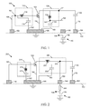
- FIG. 1 is a schematic diagram of an RF amplifier device 100.
- Device 100 includes an input terminal 102, an output terminal 104, one or more voltage reference terminals 106 (only one of which is shown in FIG. 1 ), a radio frequency (RF) cold point terminal 108, an input circuit 110, a transistor 120, and an output circuit 130, in an embodiment.
- transistor 120 and various elements of the input and output circuits 110, 130 are shown as singular components, the depiction is for the purpose of ease of explanation only. Those of skill in the art would understand, based on the description herein, that transistor 120 and/or certain elements of the input and output circuits 110, 130 each may be implemented as multiple components (e.g., connected in parallel or in series with each other).
- the description of transistor 120 and various elements of the input and output circuits 110, 130, below, are not intended to limit the scope of the inventive subject matter only to the illustrated embodiments.
- Transistor 120 is the primary active component of device 100.
- Transistor 120 includes a control terminal and first and second current conducting terminals, where the current conducting terminals are spatially and electrically separated by a variable-conductivity channel.
- transistor 120 may be a field effect transistor (FET) (such as a metal oxide semiconductor FET (MOSFET), a laterally diffused MOSFET (LDMOS FET), a high electron mobility transistor (HEMT), and so on), which includes a gate (control terminal), a source (a first current conducting terminal), and a drain (a second current conducting terminal).
- FET field effect transistor
- MOSFET metal oxide semiconductor FET
- LDM FET laterally diffused MOSFET
- HEMT high electron mobility transistor
- transistor 120 may be a bipolar junction transistor (BJT). Accordingly, references herein to a "gate,” “drain,” and “source,” are not intended to be limiting, as each of these designations has analogous features for a BJT implementation (e.g.,
- the gate of transistor 120 is coupled through the input circuit 110 to the input terminal 102, the drain of transistor 120 is coupled through the output circuit 130 to the output terminal 104, and the source of transistor 120 is coupled through the voltage reference terminal 106 to ground (or another voltage reference).
- the gate of transistor 120 may be coupled to the input terminal 102 through one or more conductive structures 160 (e.g., conductive vias or other structures), the source of transistor 120 may be coupled to voltage reference terminal 106 (e.g., a terminal coupled to ground or another voltage reference) through one or more other conductive structures 164 (e.g., conductive vias, a heavily doped sinker region, and so on), and the drain of transistor 120 may be coupled to output terminal 104 through one or more other conductive structures 170 (e.g., conductive vias or other structures).
- a DC blocking capacitor 136 may be coupled between the drain of transistor 120 and the output terminal 104, as illustrated, or the DC blocking capacitor 136 may be excluded, in other embodiments. The value of the DC blocking capacitor 136 may be selected to provide significant gain reductions at low frequencies (e.g., frequencies below the intended RF operating band).
- control signals e.g., input RF signals
- input terminal 102 functions to receive a relatively low-power, input RF signal for amplification.
- the input RF signal received through input terminal 102 is amplified through transistor 120, and the resultant amplified RF signal is output through output terminal 104.
- the input RF signal is conveyed from the input terminal 102 through the input circuit 110 to the control terminal of transistor 120.
- Input circuit 110 which functions to filter the input RF signal, is coupled between the input terminal 102 and the control terminal of transistor 120.
- input circuit 110 is an input impedance matching circuit, which is configured to raise the impedance of device 100 to a higher (e.g., intermediate or higher) impedance level (e.g., in a range from about 2 to about 10 Ohms or higher).
- Input circuit 110 is coupled to the input terminal 102 through the conductive structure(s) 160. Further, input circuit 110 may be coupled through one or more additional conductive structures 162 to voltage reference terminal 106 (or another distinct voltage reference terminal).
- input circuit 110 includes an inductive element 116 and a shunt capacitor 114. More specifically, a first plate (or terminal) of shunt capacitor 114 is electrically coupled to the input terminal 102 (e.g., through conductive structure(s) 160), and a second plate (or terminal) of shunt capacitor 114 is electrically coupled to the voltage reference terminal 106 (e.g., through conductive structure(s) 162).
- Inductive element 116 has a first terminal that also is electrically coupled to the input terminal 102 (e.g., through conductive structure(s) 160) and to the first plate of shunt capacitor 114, and a second terminal that is electrically coupled to the control terminal of transistor 120.
- the inductive element 116 may have a value in a range between about 50 picohenries (pH) to about 3 nanohenries (nH), and shunt capacitor 114 may have a value in a range between about 5 picofarads (pF) to about 80 pF, although inductive element 116 and shunt capacitor 114 may have values that fall outside of these ranges, as well.
- input circuit 110 operates as a low pass filter circuit.
- input circuit 110 may be configured as a high pass filter circuit (e.g., as in the embodiment of FIG. 2 ) or as a bandpass filter circuit (e.g., as in the embodiment of FIG. 3 ).
- Output circuit 130 which functions to filter the amplified RF signal, is coupled between the drain terminal of transistor 120 and the output terminal 104.
- output circuit 130 is an output impedance matching circuit, which is configured to match the output impedance of device 100 with the input impedance of an external circuit or component (not shown) that may be coupled to output terminal 104 (e.g., 50 Ohms or some other value).
- Output circuit 130 is coupled to the drain of transistor 120 and to output terminal 104 through one or more conductive structures 170 (e.g., conductive vias or other structures).
- output circuit 130 may be coupled through one or more additional conductive structures 166 to voltage reference terminal 106 (or another distinct voltage reference terminal).
- output circuit 130 also may be coupled through one or more additional conductive structures 168 and RF cold point terminal 108 to other external circuitry (described below).
- output circuit 130 includes a shunt inductive element 134 and a shunt capacitor 132 coupled in series. More specifically, inductive element 134 has a first terminal that is electrically coupled to the drain of transistor 120, and also to output terminal 104 (e.g., through conductive structure(s) 170). Inductive element 134 has a second terminal that is coupled to a first plate (or terminal) of shunt capacitor 132. A second plate (or terminal) of shunt capacitor 132 is electrically coupled to the voltage reference terminal 106 (or another distinct voltage reference terminal) through conductive structure(s) 166.
- shunt inductor 134 may have a value in a range between about 100 pH to about 3 nH, and shunt capacitor 132 may have a value in a range between about 50 pF to about 500 pF, although these components may have values outside of these ranges, as well.
- output circuit 130 operates as a high pass filter circuit.
- output circuit 130 may be configured as a low pass filter circuit (e.g., as in the embodiment of FIG. 2 ) or as a bandpass filter circuit (e.g., as in the embodiment of FIG. 3 ).
- the output circuitry 130 provides a single phase inversion (e.g., a 90° phase shift) that results in the phase of the signal at the output terminal 104 being shifted 90° relative to the signal at the drain of transistor 120.
- an RF "cold point” is present at the node 142 between shunt inductor 134 and shunt capacitor 132.
- node 142 may be referred to herein as an "RF cold point node.”
- the capacitance of the shunt capacitor 132 is chosen to provide a virtual ground reference voltage for the RF electrical signals at node 142, such that inductive element 134 functions as a shunt inductance to the RF ground voltage, while the inductance of the inductive element 134 is chosen to provide desired impedance at the output terminal 104 at the fundamental frequency of the amplifier 100.
- the capacitance of capacitor 132 may be chosen to be within the range of about 70 pF to about 500 pF
- the inductance of the inductive element 124 may be chosen to be within the range of about 100 pH to about 500pH, such that the output circuit 130 provides an output impedance at the output terminal 104 within the range of about 1.0 to 5.0 Ohms.
- the desired output impedance at the output terminal 104 may be an intermediate impedance that is subsequently transformed to a different value for impedance matching at the input of a power combiner (e.g., power combiner 1860, FIG. 18 ), and thus, the output impedance at the output terminal 104 will vary to suit the needs of a particular implementation.
- a power combiner e.g., power combiner 1860, FIG. 18
- the RF cold point node 142 may be coupled to an external circuit.
- the external circuit may include a voltage source, Vdd, and an envelope frequency termination circuit 140.
- the voltage source Vdd may be used to bias the transistor 120, and the envelope frequency termination circuit 140 may function to improve the low frequency resonance of device 100 caused by the interaction between the output circuit 130 and bias feeds (not shown) by presenting a high impedance at RF frequencies.
- Vdd alternatively may be provided at output terminal 104.
- the envelope frequency termination circuit 140 essentially is "invisible" from a matching standpoint, as it only effects the output impedance at envelope frequencies (i.e., envelope frequency termination circuit 140 provides terminations for the envelope frequencies of device 100).
- envelope frequency termination circuit 140 includes a capacitor 146, which may be referred to herein as an "envelope capacitor.”
- a first plate (or terminal) of envelope capacitor 146 is coupled to RF cold point terminal 108, and a second plate (or terminal) of the envelope capacitor 146 is coupled to ground (or another voltage reference), in an embodiment.
- Envelope capacitor 146 may be a discrete component, for example, and may have a value in a range between about 2.0 nanofarads (nF) to about 1.0 microfarad ( ⁇ F), although envelope capacitor 146 may have a value outside of this range, as well.
- envelope capacitor 146 may be coupled through relatively low-inductance connections to a printed circuit board (PCB) to which device 100 is coupled.
- PCB printed circuit board
- input circuit 110, transistor 120, and output circuit 130 all are implemented on a single semiconductor die (e.g., die 450, FIG. 4 ).
- the RF amplifier device 100 is monolithic.
- portions of input circuit 110 and/or output circuit 130 may be implemented as discrete components, and/or may be implemented on semiconductor die that are distinct from the semiconductor die on which transistor 120 is implemented.
- input circuit 110, transistor 120, and output circuit 130 may be formed in proximity to (e.g., below, at, and above) a top surface of the substrate.
- output terminal 104, voltage reference terminal 106, and RF cold point terminal 108 each may include a conductive feature coupled to a bottom surface of the substrate, in an embodiment.
- terminals 102, 104, 106, 108 are physically separated from each other across "conductor-less" regions of the bottom substrate surface (i.e., portions of the bottom substrate surface to which no conductive material is coupled).
- terminals 102, 104, 106, 108 enable the RF amplifier device 100 to be electrically coupled with external circuitry.
- the RF amplifier device 100 may be physically and electrically coupled to a PCB or other substrate (e.g., PCB 1610, FIG. 16 ), which includes additional circuitry of the amplifier system.
- a device plane (represented by dashed line 150) is established, where amplifier components present on one side of the device plane (e.g., components above line 150 in FIG. 1 , or "above the device plane") may be implemented on a single semiconductor substrate, and components present on the other side of the device plane (e.g., components below line 150 in FIG. 1 , or "below the device plane”) may be coupled to the PCB or other substrates.
- ground references e.g., Vdd
- other components e.g., capacitor 146
- transmission lines e.g., signal splitters, signal combiners, phase shifters, and various other amplifier components
- input circuit 110 is configured as a low pass filter
- output circuit 130 is configured as a high pass filter
- input circuit 210 may be configured as a high pass filter
- output circuit 230 may be configured as a low pass filter
- a high pass filter input circuit 210 may include a shunt inductive element 216 and a shunt capacitor 214 coupled in series. More specifically, inductive element 216 has a first terminal that is electrically coupled to the gate of transistor 120, and also to input terminal 102 (e.g., through conductive structure(s) 160).
- Inductive element 216 has a second terminal that is coupled to a first plate (or terminal) of shunt capacitor 214.
- a second plate (or terminal) of shunt capacitor 214 is electrically coupled to the voltage reference terminal 106 (or another distinct voltage reference terminal) through conductive structure(s) 162.
- a low pass filter output circuit 230 may include an inductive element 234 and a shunt capacitor 232. More specifically, a first terminal of inductive element 234 is electrically coupled to the drain of transistor 120, and a second terminal of inductive element 234 is electrically coupled to the output terminal 104 (e.g., through conductive structure(s) 170) and to a first plate (or terminal) of shunt capacitor 232. According to an embodiment, a DC blocking capacitor 136 may be coupled between the second terminal of inductive element 234 and the output terminal 104, as illustrated, or the DC blocking capacitor 136 may be excluded, in other embodiments.
- the first plate of shunt capacitor 232 also is electrically coupled to the output terminal 104 (e.g., through conductive structure(s) 170 and DC blocking capacitor 136, when included), and a second plate (or terminal) of shunt capacitor 232 is electrically coupled to the voltage reference terminal 106 (e.g., through conductive structure(s) 166).
- an RF low impedance node 242 is present between inductor 234 and DC blocking capacitor 236, when included.
- node 242 may be coupled to an external circuit (e.g., including a voltage source, Vdd, and an envelope frequency termination circuit 140).
- Vdd voltage source
- envelope frequency termination circuit 140 envelope frequency termination circuit 140
- high impedance element 244 is provided between Vdd and node 242, in an embodiment.
- the high impedance element 244 may be implemented, for example, as a quarter wave line or an inductive element.
- high impedance element 244 implemented below the device plane 150 (e.g., on a PCB to which the device is coupled), high impedance element 244 may be implemented above the device plane 150 (e.g., coupled to or monolithically formed as part of the semiconductor substrate), in another embodiment.
- terminals 104 and 108 may be replaced with a single terminal for outputting the amplified output signal, and Vdd, high impedance element 244, and/or envelope frequency termination circuit 140 may be provided at that terminal.
- either or both of the input circuit and/or output circuit may be configured as a bandpass filter.
- both input circuit 310 and output circuit 330 are configured as bandpass filters.
- bandpass filter input circuit 310 includes a low pass filter section and a high pass filter section.
- the low pass filter section includes an inductive element 316 and a shunt capacitor 314, and the high pass filter section includes a shunt inductive element 317 and a shunt capacitor 315 coupled in series.
- shunt capacitor 314 has a first plate (or terminal) coupled to input terminal 102 (e.g., through conductive structure(s) 160), and a second plate (or terminal), which is electrically coupled to the voltage reference terminal 106 (or another distinct voltage reference terminal) through conductive structure(s) 162.
- Inductive element 316 has a first terminal that is electrically coupled to the input terminal 102 (e.g., through conductive structure(s) 160), and a second terminal that is electrically coupled to the gate of transistor 120.
- a DC blocking capacitor 312 may be coupled between the first terminal of inductive element 316 and the input terminal 102, as illustrated, or the DC blocking capacitor 312 may be excluded, in other embodiments.
- Inductive element 317 has a first terminal that is coupled to the second terminal of inductive element 316, and also to the gate of transistor 120. In addition, inductive element 317 has a second terminal that is coupled to a first plate (or terminal) of shunt capacitor 315. A second plate (or terminal) of shunt capacitor 315 is electrically coupled to the voltage reference terminal 106 (or another distinct voltage reference terminal) through conductive structure(s) 162.
- an RF cold point node 318 is present between inductor 317 and shunt capacitor 315.
- the RF cold point node 318 may be coupled to an external circuit (e.g., including a voltage source, Vgg, and an envelope frequency termination circuit 340).
- Bandpass filter out circuit 330 also includes a high pass filter section and a low pass filter section.
- the high pass filter section includes a shunt inductive element 334 and a shunt capacitor 332 coupled in series
- the low pass filter section includes an inductive element 335 and a shunt capacitor 333.
- inductive element 334 has a first terminal that is coupled to the drain of transistor 120, and also to a first terminal of inductive element 335.
- inductive element 334 has a second terminal that is coupled to a first plate (or terminal) of shunt capacitor 332.
- a second plate (or terminal) of shunt capacitor 332 is electrically coupled to the voltage reference terminal 106 (or another distinct voltage reference terminal) through conductive structure(s) 166.
- Inductive element 335 has a first terminal that is electrically coupled to the drain of transistor 120 and to the first terminal of inductive element 334, and a second terminal that is coupled to the output terminal 104 (e.g., through conductive structure(s) 170).
- a DC blocking capacitor 136 may be coupled between the second terminal of inductive element 335 and the output terminal 104, as illustrated, or the DC blocking capacitor 136 may be excluded, in other embodiments.
- the second terminal of inductive element 335 also is coupled to a first plate (or terminal) of shunt capacitor 333.
- a second plate (or terminal) of shunt capacitor 333 is electrically coupled to the voltage reference terminal 106 (or another distinct voltage reference terminal) through conductive structure(s) 166.
- an RF cold point node 342 is present between inductor 334 and shunt capacitor 332.
- the RF cold point node 342 may be coupled to an external circuit (e.g., including a voltage source, Vdd, and an envelope frequency termination circuit 140).
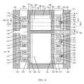
- FIGs 4 and 5 which should be viewed together for increased understanding, are top and bottom views, respectively, of a semiconductor die 450, which includes portions of two amplifier paths 400, 401, in accordance with an example embodiment.
- FIGs 6-10 also will be referenced in the description of semiconductor die 450, as those figures illustrate various cross-sectional or enlarged views of portions of die 450, and those views are helpful in understanding the various details of the embodiments. More specifically, FIGs 6 , 8, and 9 are cross-sectional, side views of die 450 along lines 6-6, 8-8, and 9-9, respectively, in FIG. 4 , and FIG. 7 is an alternative embodiment of a cross-sectional, side view of a die along a line that would correspond to line 6-6 in FIG. 4 .
- die 450 includes a semiconductor substrate 650 with top and bottom substrate surfaces 652, 654, and a plurality of dielectric and conductive layers 680 (referred to as "build-up" layers herein) formed over and coupled to the top substrate surface 652.
- build-up layers 680 referred to as "build-up" layers herein
- the lowest (i.e., closest to substrate 650) and highest (i.e., closest to the top die surface 452) build up layers 680 are depicted for simplicity, and vertical ellipses "" are included to indicate that additional dielectric and conductive layers may be included between the lowest and highest build up layers 680.
- the conductive layer 681 closest to the top substrate surface 652 may be the M1 layer (metal 1 layer), and the conductive layers 682, 683 closest to the top die surface 452 may be the M4 and M5 layers, respectively.
- conductive layers 681-683 may be formed from aluminum-copper-tungsten (AlCuW) or other commonly-used conductive layer materials.
- AlCuW aluminum-copper-tungsten
- all or portions of the metal layer (e.g., layer 683) included in inductors 416, 417, 434, 435 may include materials that are different from the materials of underlying metal layers (e.g., layers 681, 682).
- a device may have more or fewer metal layers, as well.
- inductors 416, 417, 434, 435 and capacitors 414, 415, 432, 433 as being formed from portions of particular metal layers 682, 683, the inductors 416, 417, 434, 435 and capacitors 414, 415, 432, 433 could be formed from portions of other metal layers, as well.
- the bottom substrate surface 654 corresponds to the bottom surface 554 ( FIG. 5 ) of die 450
- the top surface 658 of the build-up layers 680 corresponds to the top surface 452 of the die 450.
- the semiconductor substrate 650 may comprise silicon, silicon-on-insulator (SOI), silicon-on-sapphire (SOS), gallium arsenide (GaAs), gallium nitride (GaN), GaN on silicon carbide, GaN on silicon, or other types of substrate materials.
- the substrate 650 may have a thickness 651 in a range of about 50 microns to about 100 microns (e.g., about 75 microns), although the substrate 650 may be thinner or thicker, as well.
- the substrate 650 may include, for example, a base semiconductor substrate and one or more additional semiconductor layers epitaxially formed on the surface of the base semiconductor substrate.
- the substrate 650 is a high-resistivity silicon substrate (e.g., a silicon substrate having bulk resistivity in a range of about 1000 ohm/centimeter (cm) to about 100,000 ohm/cm or greater).
- the substrate 650 may be a semi-insulating GaAs substrate (e.g., a GaAs substrate having bulk resistivity up to 10 8 ohm/cm), or another suitable high-resistivity substrate.
- top and bottom substrate surfaces 652, 654 may be made using conductive through substrate vias (TSVs) (e.g., TSVs 661, 664, 671, 863, 865, 869, FIGs 6 , 8 ).
- TSVs conductive through substrate vias
- electrical connections between top and bottom substrate surfaces 652, 654 may be made using wrap-around terminations (e.g., wrap-around terminations 760, 770, FIG. 7 ) or using other conductive structures.
- wrap-around terminations e.g., wrap-around terminations 760, 770, FIG. 7
- Still other embodiments may be implemented using low-resistivity substrates.
- each amplifier path 400, 401 includes an input circuit (e.g., input circuit 110, FIG. 1 ) that includes at least one inductor 416, 417 (e.g., inductive element 116, FIG. 1 ) and at least one capacitor 414, 415 (e.g., capacitor 114, FIG. 1 ), a transistor 420, 421 (e.g., transistor 120, FIG. 1 ), and an output circuit (e.g., output circuit 130, FIG. 1 ) that includes at least one inductor 434, 435 (e.g., inductive element 134, FIG.
- an input circuit e.g., input circuit 110, FIG. 1
- each amplifier path 400, 401 includes at least one inductor 416, 417 (e.g., inductive element 116, FIG. 1 ) and at least one capacitor 414, 415 (e.g., capacitor 114, FIG. 1 ), a transistor 420, 421 (e.g., transistor 120, FIG. 1 ), and an
- each amplifier path 400, 401 is a single stage amplifier (e.g., each including one power transistor 420, 421).
- each amplifier path may be implemented as a multi-stage amplifier (e.g., with a pre-amplifier transistor in series with a final amplifier transistor).
- a matching circuit may be implemented between the pre-amplifier and final amplifier stages.
- the active and passive components of die 450 are electrically coupled to each other and to a plurality of conductive features 502, 503, 504, 505, 506 (e.g., conductive components 102, 104, 106, 108, FIG. 1 ) that are coupled to the bottom substrate surface 654.
- Those conductive features 502-506 facilitate electrical connection of the die's active and passive components to external circuitry (e.g., circuitry 140, FIG. 4 , and 1850, 1852, 1860, 1862, FIG. 18 ).
- FIGs 5 , 6 , 8, and 9 Various views of the plurality of conductive features 502-506 are shown in FIGs 5 , 6 , 8, and 9 . Because the relative locations of the conductive features 502-506 with respect to the other circuitry that overlies the top substrate surface 652 is relevant to the inventive subject matter, the conductive features 502-506 also are indicated in FIG. 4 , although with dashed borders to indicate that they are not proximate to the top substrate surface 652, but instead are coupled to the bottom die surface 554.
- Each of the conductive features 502-506 only partially covers the bottom die surface 554 to define a number of conductor-less regions 580, 582, 584, 586 that span various portions of the bottom die surface 554.
- a "conductor-less region” is a portion of the bottom die surface 554 to which no conductive material (or at least no significant quantity of conductive material) is coupled.
- the various conductive features 502-506 are electrically isolated from each other across the bottom die surface 554 by the conductor-less regions 580, 582, 584, 586. Conductor-less regions 584, 586 provide for electrical separation of the input signals provided to amplifier paths 400, 401.
- conductor-less regions 580, 582 are located directly opposite (in a vertical direction, with respect to FIG. 6 ) portions 480, 482 of the top substrate surface 652 over which inductors 416, 417, 434, 435 are formed. Because the voltage reference plane is lacking under inductors 415, 417, 434, 435 in the device, according to the various embodiments, inductors 415, 417, 434, 435 may be referred to herein as "floating" inductors. Inclusion of the conductor-less regions 580, 582 under floating inductors 415, 417, 434, 435 may achieve multiple advantages, as will be discussed in more detail later.
- the conductive features 502-506 each may form a portion of a patterned conductive layer 655 that is coupled to the bottom substrate surface 654, where voids in the patterned conductive layer 655 correspond to the conductor-less regions 580, 582, 584, 586. Some or all of the conductive features 502-506 may be directly connected to the bottom substrate surface 654, or an insulating layer 656 may be present between some or all of the conductive features 502-506 in order to electrically isolate them from the substrate 650, in various embodiments.
- conductive layer 655 includes plated copper (i.e., multiple layers applied using a plating process) or other conductive metal or metal alloy, and conductive layer 655 has a thickness 657 in a range of about 10 microns to about 50 microns.
- the patterned conductive layer 655 may be formed from one or more layers of a single conductive material, or may be formed from layers of different materials.
- the patterned conductive layer 655 may be thinner or thicker than the above-given range.
- the conductive features 502-506 may be distinct structures that are otherwise coupled (e.g., bonded, soldered, adhered, and so on) to the bottom substrate surface 654.
- Conductive features 502, 503 represent input terminals (e.g., two instances of terminal 102, FIG. 1 ) for the first and second amplifier paths 400, 401, respectively, and conductive features 504, 505 represent output terminals (e.g., two instances of terminal 104, FIG. 1 ) for the first and second amplifier paths 400, 401, respectively.
- Conductive feature 506 represents a voltage reference terminal (e.g., voltage reference terminal 106, FIG. 1 ), and although the voltage reference terminal is depicted as a single conductive feature 506 in the illustrated embodiments, a set of distinct and separate conductive features alternatively may serve as a plurality of voltage reference terminals, in an alternate embodiment.
- conductive features 508, 509 represent terminals (e.g., three instances of terminal 108, FIG. 1 ) that enable portions of the amplifier paths 400, 401 to be coupled to other external circuitry.
- conductive features 508, 509 may represent RF cold point node terminals (e.g., multiple instances of RF cold point node terminal 108), which enable RF cold points (e.g., node 148, FIG. 1 ) to be coupled with external circuitry (e.g., with envelope frequency termination circuitry 140, FIG. 1 ).
- the nodes between inductors 434, 435 and capacitors 432, 433 represent RF cold point nodes.
- conductive features 508, 509 may enable a bias voltage (e.g., Vdd) to be provided to the drain terminals 424, 425 of transistors 420, 421 of each amplifier path 400, 401.
- a bias voltage e.g., Vdd
- similar conductive features may be provided to an RF cold point node in the input circuit, to provide the ability to provide a bias voltage to be provided to the control terminals 422, 423 of transistors 420, 421, as well.
- conductive feature 502 which is configured to receive an input RF signal, is electrically connected to the input circuit (e.g., input circuit 110, FIG. 1 ) through a first set of conductive structures 660 (e.g., conductive structures 160, FIG. 1 ) that provide a continuous electrical path between conductive feature 502 and an input node 461 to the input circuit (e.g., node 161, FIG. 1 ).
- the first set of conductive structures 660 may include one or more TSVs 661, portions of conductive layers 681-683, and conductive vias 663 that electrically couple the portions of the conductive layers 681-683.
- TSVs 661 may be electrically isolated from substrate 650 with dielectric via lining material 662, in an embodiment, although lining material 662 may be excluded, in other embodiments.
- the input circuit for path 400 includes inductors 416 (e.g., parallel instances of inductor 116, FIG. 1 ) and capacitor 414 (e.g., capacitor 114, FIG. 1 ), and the input circuit for path 401 includes inductors 417 (e.g., parallel instances of inductor 116, FIG. 1 ) and capacitors 415 (e.g., capacitor 114, FIG. 1 ). More specifically, the input circuit for path 400 includes inductors 416, which are coupled in parallel between node 461 and the control terminal 422 (e.g., gate) of transistor 420 (e.g., transistor 120, FIG. 1 ).
- transistor 420 e.g., transistor 120, FIG. 1
- the input circuit for path 401 includes inductors 417, which are coupled in parallel between conductive structure 461 and the control terminal 423 of transistor 421.
- inductors 416, 417 is implemented as an integrated spiral inductor formed from portions of one or more conductive layers (e.g., layers 682, 683).
- the spiral inductors may be formed from as few as one conductive layer or from multiple conductive layers, with conductive vias interconnecting the inductor portions, and cross-overs and cross-unders implemented, as appropriate.
- a first (input) terminal of each inductor 416, 417 is coupled to the input node of its respective input circuit, and a second (output) terminal of each inductor 416, 417 is coupled through portions 418, 419 of a conductive layer (e.g., conductive layer 682) to the control terminals 422, 423 of transistors 420, 421.
- a conductive layer e.g., conductive layer 682
- capacitors 414, 415 are coupled between the input circuit input node (e.g., node 461 for path 400) and voltage reference terminal 506 (e.g., terminal 106, FIG. 1 ). More specifically, a first plate (or electrode) 814 of capacitor 414 is coupled to node 461 (and thus to the input terminal of inductor 416), and a second plate (or electrode) 815 of capacitor 414 is coupled to the voltage reference terminal 506 through conductive structures 862 (e.g., conductive structures 162, FIG. 1 ). Capacitors 415 are similarly coupled between conductive structure 461 and the voltage reference terminal 506.
- capacitors 414, 415 are implemented as metal-insulator-metal (MIM) capacitors, each of which includes vertically aligned portions of two conductive layers 683, 682 (e.g., the first and second capacitor plates 814, 815) and inter-layer dielectric between the capacitor plates 814, 815.
- conductive structures 862 may include one or more TSVs 863, portions of conductive layers 681, 682, and conductive vias 864 that electrically couple the portions of the conductive layers 681, 682.
- TSVs 863 may be electrically isolated from substrate 650 with dielectric via lining material, in an embodiment, although lining material may be excluded, in other embodiments.
- transistors 420, 421 may be LDMOS FET transistors, for example.
- Each transistor 420, 421 includes a control terminal 422, 423 (e.g., gate), a first current conducting region (e.g., a drain region coupled to a drain terminal 424, 425), and a second current conducting region (e.g., a source region).
- the control terminal is coupled to the input circuit 110, one of the current conducting regions (e.g., the drain region) is coupled to the output circuit 130, and the other current conducting region (e.g., the source region) is coupled to a voltage reference.
- FIG. 10 which is a top view of portion 10 ( FIG. 4 ) of transistor 420, additional details of transistor 420 will now be described. Reference also will be made to the cross-sectional view of FIG. 6 , for clarity.
- transistor 420 includes an active area 610, with a plurality of substantially parallel-aligned drain regions 1025 and source regions 1030 (outlined with dashed rectangles) formed in the substrate 650 below the top substrate surface 652. Due to their elongated shapes and interdigitated arrangements, the drain and source regions 1025, 1030 may be referred to as "fingers.” In any event, drain regions 1025 are electrically coupled to conductive (e.g., metal) drain finger contacts 1024, each of which extends to drain contact 424. Source regions 1030 are electrically coupled to conductive (e.g., metal) source finger contacts 1062, which in turn are coupled to conductive TSVs 664 ( FIG.
- TSVs 664 may or may not be lined with dielectric material to insulate the TSVs 664 from the substrate 650, in various embodiments.
- a variably-conductive channel and, in some embodiments, a drain drift region are present between adjacent source and drain regions 1030, 1025 of each transistor finger.
- Conductive (e.g., polysilicon) gate structures 1022 are coupled to and extend from gate contact 422 across the channel regions so that voltages applied to the gate contact 422 during operation may modulate the conductivity of the channels, and thus the current flow between source and drain regions 1030, 1025 (or ultimately between conductive feature 506 and drain contact 424).
- LDMOS FET Although a particular layout of an LDMOS FET is illustrated in FIG. 10 , it should be understood that many different layouts may be implemented to provide the transistor(s), in various embodiments. For example, in some embodiments, doped sinker regions may be used to provide portions of the electrical path between the source regions and the conductive feature 506 at the bottom substrate surface 654. Numerous other modifications also may be made, depending on the characteristics of the selected substrate and the operation and performance of the transistor.
- drain terminals 424, 425 of transistors 420, 421 are electrically coupled to conductive features 504, 505 (e.g., two instances of terminal 104, FIG. 1 ) and also to output circuits (e.g., two instances of output circuit 130, FIG. 1 ).
- conductive features 504, 505 e.g., two instances of terminal 104, FIG. 1
- output circuits e.g., two instances of output circuit 130, FIG. 1 .
- FIG. 4 illustrates multiple instances of conductive features 472, 474 extending between drain terminals 424, 425 and nodes 471, 473 (e.g., multiple instances of node 171, FIG. 1 ).
- Conductive features 472, 474 may include, for example, portions of one or more conductive layers 681-683 and conductive vias interconnecting the drain terminals 424, 425 and the portions of the conductive layers 681-683, as appropriate.
- nodes 471, 473 are electrically coupled to the conductive features 504, 505 (and thus the drain terminals 424, 425 are electrically coupled to the conductive features 504, 505).
- FIG. 6 depicts node 471 as being coupled to conductive feature 504 through a set of conductive structures 670 (e.g., node 171 is coupled to terminal 104 through conductive structure 170, FIG. 1 ).
- the set of conductive structures 670 provides a continuous electrical path between node 471 and conductive feature 504.
- the set of conductive structures 670 may include one or more TSVs 671, portions of conductive layers 681-683, and conductive vias 673 that electrically couple the portions of the conductive layers 681-683.
- TSVs 671 may be electrically isolated from substrate 650 with dielectric via lining material 672, in an embodiment, although lining material 672 may be excluded, in other embodiments.
- conductive features 504, 505 are configured to output the amplified RF signals produced by transistors 420, 421.
- the drain terminals 424, 425 also are electrically connected to the output circuits (e.g., two instances of output circuit 130, FIG. 1 ).
- the output circuit for path 400 includes inductors 434 (e.g., parallel instances of inductor 134, FIG. 1 ) and capacitor 432 (e.g., capacitor 132, FIG. 1 ), and the output circuit for path 401 includes inductors 435 (e.g., parallel instances of inductor 134, FIG. 1 ) and capacitors 433 (e.g., capacitor 132, FIG. 1 ).
- the output circuit for path 400 includes inductors 434, which are coupled in parallel between drain terminal 424 (or node 471) and node 442 (e.g., node 142, FIG. 1 ).
- the output circuit also includes capacitor 432, which is coupled between node 442 and conductive feature 506 through another set of conductive structures 866.
- Each of inductors 434, 435 is implemented as an integrated spiral inductor formed from portions of one or more conductive layers (e.g., layers 682, 683).
- the spiral inductors may be formed from as few as one conductive layer or from multiple conductive layers, with conductive vias interconnecting the inductor portions, and cross-overs and cross-unders implemented, as appropriate.
- at least the portion of top conductive layer 683 that includes inductors 416, 417, 434, 435 may be formed from or include a material that is different from (e.g., more highly conductive than) the material(s) from which the lower metal layers 681, 682, and/or other portions of layer 683 are formed. For example, as illustrated in FIG.
- portions of layer 683 corresponding to inductors 416, 417, 434, 435 may include multiple conductive material layers 684, 685.
- the bottom conductive material layer 684 may comprise AlCuW (or some other material), as discussed previously, and the top conductive material layer 685 may comprise copper (Cu) or some other highly conductive material.
- the portions of layer 683 corresponding to some or all of inductors 416, 417, 434, 435 may include a single layer of the more highly conductive material (e.g., Cu).
- the inclusion of the highly conductive material may increase the Q of inductors 416, 417, 434, 435, which may be particularly advantageous for inductors 434, 435 in the output circuit, since the Q of inductors 434, 435 on the higher-power side of the amplifier path 400 may more significantly affect the efficiency of the amplifier than the Q of inductors 416, 417 on the lower-power side of the amplifier path 400.
- the portions of layer 683 corresponding to some or all of inductors 416, 417, 434, 435 may include substantially the same materials as the other layers 681, 682.
- a first (input) terminal of each inductor 434, 435 is coupled though portions 436, 437 of a conductive layer (e.g., conductive layer 682) to the drain terminal 424, 425 of transistors 420, 421, respectively.
- a second (output) terminal of each inductor 434, 435 is coupled to nodes 442, 444.
- the values of inductor 434 and capacitor 432 may be selected so that node 442 (or node 142, FIG. 1 ) between inductor 434 and capacitor 432 functions as an RF cold point node.
- capacitors 432, 433 are coupled between node 442 for path 400) and voltage reference terminal 506 (e.g., terminal 106, FIG. 1 ). More specifically, a first plate (or electrode) 816 of capacitor 432 is coupled to node 442 (and thus to the output terminal of inductor 434), and a second plate (or electrode) 817 of capacitor 432 is coupled to the voltage reference terminal 506 through conductive structures 866 (e.g., conductive structures 166, FIG. 1 ). Capacitors 433 are similarly coupled between nodes 444 and the voltage reference terminal 506.
- capacitors 432, 433 are implemented as MIM capacitors, each of which includes vertically aligned portions of two conductive layers 683, 682 (e.g., the first and second capacitor plates 816, 817) and inter-layer dielectric between the capacitor plates 816, 817.
- conductive structures 866 may include one or more TSVs 865, portions of conductive layers 681, 682, and conductive vias 867 that electrically couple the portions of the conductive layers 681, 682.
- TSVs 865 may be electrically isolated from substrate 650 with dielectric via lining material, in an embodiment, although lining material may be excluded, in other embodiments.
- die 450 includes further conductive features that electrically couple RF cold point nodes 442, 444 to terminal 508, 509 (e.g., multiple instances of terminal 108, FIG. 1 ), which provides the ability to couple external circuitry (e.g., circuitry 140, FIG. 1 ) to the RF cold point nodes 442, 444.
- die 450 includes conductive structures 868 (e.g., conductive structures 168, FIG. 1 ) that electrically couple RF cold point node 442 and terminal 508.
- Conductive structures 868 may include one or more TSVs 869, portions of conductive layers 681-683, and conductive vias 871 that electrically couple the portions of the conductive layers 681-683.
- TSVs 869 may be electrically isolated from substrate 650 with dielectric via lining material 870, in an embodiment, although lining material 870 may be excluded, in other embodiments.
- conductive structures 660, 670, 862, 866, 868 are used to provide electrical connections between components formed over the top substrate surface 652 and conductive features 502-506 coupled to the bottom substrate surface 654.
- alternative conductive structures may be implemented to replace all or portions of conductive structures 660, 670, 862, 866, 868. For example, in an alternate embodiment depicted in FIG. 7 (which corresponds in location to the cross-sectional view of FIG.
- conductive structures 660, 670 may be replaced with conductive wrap-around terminations 760, 770 which are coupled to side surfaces of die 750 to interconnect conductive features 702, 704 with the input and output circuits located over the top substrate surface 752.
- the wrap-around terminations 760, 770 may be electrically isolated from substrate 752 with dielectric material 762, 772, in an embodiment, although the dielectric material 762, 772 may be excluded, in other embodiments.
- other types of conductive structures e.g., printed conductive lines, wirebonds, and so on
- some or all of conductive structures 862, 866, 868 may be similarly replaced with wrap-around terminations or other types of conductive structures.
- Die 450 is shown to include portions of two parallel amplifier paths 400, 401.
- one or more isolation features 490 may be embedded within the die 450, within encapsulant 490, or otherwise interposed between the parallel amplification paths 400, 401 in order to reduce potential signal interference between the two paths.
- the transistors 420, 421 of amplifier paths 400, 401 are of different sizes, as indicated by their different areas. Accordingly, the transistors 420, 421 may have different current-carrying capacities. For example, transistor 421 may be capable of handling twice the current of transistor 420.
- Such an arrangement may be particularly advantageous, for example, in an asymmetric Doherty amplifier (e.g., Doherty amplifier 1800, FIG.
- transistors 420, 421 may be substantially the same in size and/or current carrying capacity (e.g., for use in a symmetric Doherty amplifier or another type of amplifier).
- die 450 is shown to include two parallel amplifier paths 400, 401, alternate embodiments of die may include a portion of a single amplifier path. Still other alternate embodiments of die may include portions of more than two amplifier paths.
- the first and second amplifier paths 400, 401 may correspond to main and peaking amplifier paths, respectively, of a Doherty amplifier.
- the first and second amplifier paths 400, 401 may be incorporated into other types of amplifiers, as well.
- amplifier path 400 will be described in detail, it being understood that amplifier path 401 includes substantially similar features.
- FIGs 4-10 embody circuitry corresponding to the amplifier configuration 100 of FIG. 1
- alternate embodiments of IC devices may embody differently configured amplifiers (e.g., amplifiers 200, 300, FIGs 2 , 3 , or other differently configured amplifiers).
- a common aspect to the various embodiments is the inclusion of one or more "floating" inductors in the input and/or output circuits of an amplifier path. Those of skill in the art would understand, based on the description herein, how to incorporate one or more of such floating inductors into differently configured amplifier ICs.
- FIG. 11 is a flowchart of a method of manufacturing a device (e.g., device 1800, 1900, 2300, 2400, FIGs 18, 19 , 23 , 24 ) that includes at least a portion of an amplifier.
- a device e.g., device 1800, 1900, 2300, 2400, FIGs 18, 19 , 23 , 24
- the die 450 may be coupled to leads (e.g., leads 1202-1205, FIG. 12 ), and the leaded assembly (e.g., device 1400, FIG.
- the completed device then may be coupled (e.g., soldered) to a PCB (e.g., PCB 2510, FIG. 25 ) that includes other portions of an amplifier.
- a PCB e.g., PCB 2510, FIG. 25
- wafer manufacturing techniques are used to fabricate a wafer that includes a multitude of instances of the above-described amplifier circuitry (e.g., a multitude of die sites, each of which includes the circuitry of die 450).
- fabrication of the wafer includes processes in which vias (e.g., vias 661, 664, 671, 863, 865, 869) are formed through a semiconductor substrate (e.g., substrate 650), and various active devices (e.g., transistors 420, 421) and passive devices (e.g., inductors 416, 417, 434, 435 and capacitors 415, 415, 432, 433), along with their interconnections, are formed in and over a top surface of the wafer.
- vias e.g., vias 661, 664, 671, 863, 865, 869
- active devices e.g., transistors 420, 421
- passive devices e.g., inductors 416, 417, 434
- the back side of the wafer may then be thinned to a desired thickness, which exposes bottom-side ends of the vias.
- Conductive features e.g., conductive features 502, 504, 506, 508 are then coupled to the bottom surface of the thinned wafer.
- a thick patterned back metal layer may be applied to the bottom surface of the wafer produce the conductive features.
- the wafer is diced along saw streets to singulate the individual die (e.g., die 450) from the wafer.
- packaging essentially includes coupling each singulated die to a leadframe, in block 1106, encapsulating the die and leadframes, in block 1108, and coupling a heatsink to the device, in block 1110.
- FIG. 12 illustrates a matrix leadframe 1200, which includes a plurality of sets of leadframe features arranged in rows in columns.
- the leadframe feature sets may be arranged in a strip (or single row), rather than a matrix.
- each set of leadframe features includes two conductive input-side leads 1202, 1203, and two conductive output-side leads 1204, 1205.
- each set of leadframe features may include more or fewer input and/or output leads, and/or may include additional leads (e.g., for biasing, coupling to external circuitry, and so on).
- the leads 1202-1205 may have a thickness in a range of about 0.15 millimeter (mm) and about 0.25 mm, in an embodiment, although the leads 1202-1205 may be thinner or thicker, as well.
- the various leadframe features 1202-1205 are structurally coupled together by sacrificial rails 1220 and sacrificial connectors 1222. To clearly differentiate the leadframe features 1202-1205 from the sacrificial features 1220, 1222, the leadframe features 1202-1205 are cross-hatched in FIG. 12 . In actuality, the leadframe and sacrificial features 1202-1205, 1220, 1222 may be integrally formed from the same material (e.g., a stamped, skived or milled leadframe formed from copper or another material), in some embodiments. Alternatively, some or all of the leadframe and sacrificial features 1202-1205, 1220, 1222 may be formed from distinct structures that are otherwise coupled together. For example, the leads 1202-1205 may be distinct structures that are staked to the sacrificial features 1220, 1222.
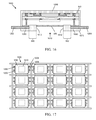
- a singulated die 450 may be coupled to each leadframe set in block 1106 to produce a partially-completed device 1300. More specifically, and as more clearly indicated in FIG. 14 , which is a cross-sectional view through line 14-14 of FIG. 13 , the conductive features 502-506 on the bottom die surface are coupled to corresponding leadframe features 1202-1205. For example, conductive features 502, 503 corresponding to signal inputs for amplifier paths 400, 401 may be coupled to leads 1202, 1203, respectively, and conductive features 504, 505 corresponding to signal outputs for amplifier paths 400, 401 may be coupled to leads 1204, 1205, respectively, in an embodiment.
- Coupling of the die 450 to the leadframe features 1202-1205 may be accomplished, for example, using solder, conductive adhesive, brazing, sintering, or other die attach techniques. Although only a single die 450 is shown to be coupled to conductive features 1202-1205, alternate embodiments may include additional conductive features (not illustrated) to which one or more additional die and/or devices are coupled, where the additional die and/or devices may include one or more additional LDMOS FETs, other types of die (e.g., integrated passive devices and/or other types of die), and/or discrete components.
- the partially completed devices 1300 may be encapsulated, in block 1108.
- FIGs 15 and 16 depict encapsulation of only one partially completed device 1300, and the below description may refer to encapsulating a single device 1300, it is to be understood that a plurality of devices may be encapsulated simultaneously (e.g., all devices 1300 coupled to leadframe 1200).
- the partially completed device 1300 is encapsulated with one or more openings (e.g., openings 1610, 2110, 2114, FIGs 16 , 21 ) for subsequent insertion and attachment of a heatsink (e.g., heatsink 1810, 1910, 2310, 2410, FIGs 18, 19 , 23 , 24 ) to the device.
- a heatsink e.g., heatsink 1810, 1910, 2310, 2410, FIGs 18, 19 , 23 , 24
- encapsulation may be performed using transfer molding (including film assisted molding), injection molding, compression molding, or other techniques.
- transfer molding a mold with top and bottom mold members 1510, 1520 may be used, where the top and bottom mold members 1510, 1520 include mold cavities 1512, 1522 that are configured to define the shape of the encapsulant material (e.g., encapsulant material 1690, FIG. 16 ) that is applied to the partially-completed device 1300.
- encapsulant material e.g., encapsulant material 1690, FIG. 16
- a plastic film 1530, 1532 is sucked onto inner surfaces 1512, 1522 of the top and bottom mold members 1510, 1520, and the lead frame 1200 with the partially completed device 1300 is inserted into the mold.
- portions 1514, 1524, of the mold inner surfaces 1512, 1522 are compressed against portions of the leads 1202-1205 to mask those portions of the leads 1202-1205 from the encapsulant material 1690.
- the bottom mold member 1520 includes a protrusion 1526 with a surface 1528 that compresses against the conductive feature 506. The surface 1528 masks the conductive feature 506 from the encapsulant material 1690, and the shape of the protrusion 1526 defines the shape of a subsequently formed encapsulant opening 1610. Further, the shape of mold cavities 1522 defines the shape of encapsulant material 1690 that will be subsequently coupled to the bottom of the device.
- each mold cavity 1522 has a first portion that underlies conductor-less regions 580, 582 (e.g., referring to FIG. 6 , regions that are located directly opposite, in a vertical direction, portions 480, 482 of the top substrate surface 652 over which inductors 416, 417, 434, 435 are formed).
- the mold cavities 1522 have second portions that underlie portions of the leads 1202-1205, in an embodiment.
- encapsulant material 1690 e.g., thermoset plastic or resin
- the mold is held in position until the encapsulant material 1690 is solidified (i.e., cured).
- the mold is then opened, and the lead frame 1200 with the encapsulated device 1600 is removed.
- the encapsulant material 1690 includes a top portion that overlies the die 450, and bottom portions that underlie the die 450 and partially encapsulate the leads 1202-1205.
- the bottom portions of encapsulant material 1690 have first portions that underlie conductor-less regions 580, 582, and second portions that underlie portions of the leads 1202-1205, in an embodiment.
- the portions of encapsulant material 1690 underlying the conductor-less regions 580, 582 contribute to the distance between inductors 415, 416, 434, 435 and the bottom or "outer" surface 1620 of device 1600 (or the height of non-conductive material between inductors 415, 416, 434, 435 and the bottom surface 1620). Further, the portions of encapsulant material 1690 underlying the leads 1202-1205 may provide electrical isolation for the leads 1202-1205.
- the shape of protrusion 1526 defines the shape of opening 1610 in the encapsulant material 1690. More particularly, the opening 1610 exposes conductive feature 506, and the opening 1610 is defined by encapsulant sidewalls 1612 that extend from the outer surface 1620 of the encapsulant material 1690 toward the bottom die surface 554 ( FIG. 6 ).
- FIG. 17 is a top view of the leadframe 1200 after encapsulation
- the encapsulant material 1690 covers the top surfaces of the dies 450
- encapsulant openings 1610 (depicted with dashed boxes in FIG. 17 since the openings 1610 would be visible only from a bottom view) expose each conductive feature 506.
- the multiple encapsulated devices are separated, in block 1108, by removing the sacrificial features 1220, 1222 of the leadframe assembly 1200.
- a heatsink 1810 is then inserted into opening 1610 and attached to conductive feature 506, resulting in a completed device 1800.
- the heatsink 1810 has first and second surfaces 1812, 1814, and heatsink sidewalls 1816 extending between the first and second surfaces 1812, 1814.
- the heatsink 1810 is positioned within the opening 1610 in the encapsulant material 1690, and the first heatsink surface 1812 is attached to conductive feature 506.
- Attaching the heatsink 1810 to the conductive feature 506 may be accomplished, for example, using solder 1830, using conductive adhesive, performing a brazing process, performing a sintering process (e.g., silver sintering), or using other die attach techniques.
- the heatsink 1810 may be pre-plated prior to attachment.
- the heatsink 1810 has a width that is substantially the same as the width of opening 1610.
- the heatsink 1810 may be press-fit into the opening 1610 so that the heatsink sidewalls 1816 are frictionally coupled with the encapsulant sidewalls 1612.
- the heatsink sidewalls 1816 are not "directly bonded" to the encapsulant sidewalls 1612, where "directly bonded,” as used herein, means in direct contact with and rigidly coupled to (as opposed to "frictionally coupled,” which is a removably coupled configuration).
- the width of the heatsink 1810 may be slightly smaller than the width of opening 1610 to facilitate insertion of the heatsink 1810 into the opening 1610 (e.g., there may be a gap between the encapsulant sidewalls 1612 and the heatsink sidewalls 1816).
- an adhesive material (not shown) may be disposed in the gap.
- the heatsink 1810 is not present directly underneath the previously-discussed conductor-less regions 580, 582 ( FIG. 5 ) under floating inductors 415, 417, 434, 435 ( FIG. 4 ). Further, the heatsink 1810 has a thickness 1820 that is sufficient to cause the heatsink 1810 to extend beyond the bottom surface 1620 of the encapsulant material 1690. In alternate embodiments, the heatsink 1810 maybe narrower, thicker or thinner. Further, as depicted in FIG. 19 , a differently-configured heatsink 1910 may be coupled to the conductive feature 506. In the embodiment illustrated in FIG.
- the heatsink 1910 has a first portion 1912 that extends into the opening 1610 and couples to the conductive feature 506, and a second portion 1914 that is wider than the opening 1610 and couples to the bottom surface 1620 of the encapsulant material 1690.
- the first portion 1912 of the heatsink 1910 has sidewalls 1916 that are not directly bonded to the encapsulant sidewalls 1612.
- the device may include multiple openings in the bottom surface of the encapsulant material 1690, and multiple heatsinks may be coupled to the die through the multiple openings.
- the device also may include openings in the top surface of the encapsulant.
- a mold with top and bottom mold members 2010, 2020 again may be used.
- the bottom mold member 2020 includes a protrusion 2026 with a surface 2028 that compresses against the conductive feature 506 of the die 450.
- the top mold member 2010 also includes a protrusion 2016, and that protrusion 2016 has a surface 2018 that compresses against the top surface of the die 450 (e.g., a portion of the top surface that overlies transistor 420, FIG. 4 ).
- the surface 2028 masks the conductive feature 506 from the encapsulant material 2190, and the surface 2018 masks a portion of the top surface of the die 450.
- the shapes of the protrusions 2016, 2026 define the shapes of subsequently formed encapsulant openings 2110, 2114.
- the shapes of mold cavities 2012, 2022 defines the shape of the encapsulant material 2190 that is subsequently coupled to the device.
- encapsulant material 2190 e.g., thermoset plastic or resin
- the portions of encapsulant material 2190 underlying the conductor-less regions 580, 582 contribute to the distance between inductors 415, 416, 434, 435 and the bottom or "outer" surface 2120 of device 2100 (or the height of non-conductive material between inductors 415, 416, 434, 435 and the bottom surface 2120).
- the portions of encapsulant material 2190 underlying the leads 1202-1205 may provide electrical isolation for the leads 1202-1205.
- the shape of protrusion 2016 defines the shape of opening 2114 in the encapsulant material 2190
- the shape of protrusion 2026 defines the shape of opening 2110 in the encapsulant material 2190.
- Opening 2110 exposes conductive feature 506, and opening 2110 is defined by encapsulant sidewalls 2112 that extend from the outer surface 2120 of the encapsulant material 2190 toward the bottom die surface 554 ( FIG. 6 ).
- FIG. 22 is a top view of the leadframe 1200 after encapsulation
- the encapsulant material 2190 covers most of the top surfaces of the dies 450, except for the portions of the dies 450 that are exposed through the openings 2114.
- the illustrated embodiment depicts an embodiment in which a portion of the dies 450 are exposed through the openings 2114, in an alternate embodiment, a layer of encapsulant material may be present over the top surface of each die 450.
- a heatsink 2310, 2410 with one of the previously-described configurations (or with a different configuration) is inserted into opening 2110 and attached to conductive feature 506, resulting in a completed device 2300, 2400.
- the heatsink sidewalls 2316, 2416 are not "directly bonded" to the encapsulant sidewalls 2112. Instead, the heatsink 2310, 2410 is either press-fit into opening 2110, or an adhesive material (not shown) is present in a gap between the heatsink sidewalls 2316, 2416 and the encapsulant sidewalls 2112.
- an additional heatsink also may be coupled to the top surface of the die 450 through opening 2114.
- any of the above-described devices 1800, 1900, 2300, 2400 may then be coupled to an electrical system, in block 1112.
- the electrical system may have additional circuitry configured to provide one or more input RF signals (e.g., to leads 1202, 1203), to receive amplified RF signals produced by the device (e.g., through leads 1204, 1205), and to provide a voltage reference (e.g., ground, through heatsink 1810, 1910, 2310, 2410).
- a voltage reference e.g., ground, through heatsink 1810, 1910, 2310, 2410.
- the device 2300 may include, for example, coupling the device 2300 to a PCB 2510, which includes one or more dielectric material layers 2520 (e.g., FR-4 or other PCB dielectrics) and one or more conductive layers 2530, 2532.
- a PCB 2510 which includes one or more dielectric material layers 2520 (e.g., FR-4 or other PCB dielectrics) and one or more conductive layers 2530, 2532.
- the PCB 2510 may include more than one dielectric material layer, and/or more than two conductive layers.
- the device 2300 may be coupled to a substrate other than a PCB.
- each lead 1202-1205 may be soldered or otherwise coupled to corresponding pads or traces formed from a first conductive layer 2530 of the PCB 2510.
- an opening 2540 in the PCB 2510 is sized to accept the heatsink 2310.
- the thickness of the heatsink 2310 and the thickness of the PCB 2510 may be selected so that the bottom surface 2312 of the heatsink 2310 is flush with the bottom surface 2512 of the PCB 2510 when the heatsink 2310 is fully inserted into the opening 2540.
- the bottom surface 2312 of the heatsink 2310 and a second conductive layer 2532 at the bottom surface 2512 of the PCB 2510 then may be coupled (e.g., soldered) to a substantially planar system heatsink (not illustrated).
- the system heatsink may have a protrusion (not illustrated) that is configured to extend into opening 2540, in which case the bottom surface 2312 of the heatsink 2310 may be recessed from the bottom surface 2512 of the PCB 2510.
- the system heatsink may have a depression (not illustrated) that is configured to receive a bottom portion of the heatsink 2310, in which case the bottom surface 2312 of the heatsink 2310 may protrude past the bottom surface 2512 of the PCB 2510. Either way, the heatsink 2310 may function both as a heatsink and as a connection to a voltage reference (e.g., ground), when the system heatsink is coupled to the voltage reference.
- a voltage reference e.g., ground
- the vertical distance 2550 between the floating inductors 416, 434 and the voltage reference plane is substantially greater than the distance 2552 between the floating inductors 416, 434 and the patterned conductive layer 655 on the bottom surface of die 450.
- distance 2550 may be in a range of about 5 mils to about 50 mils or more, depending on the cumulative thickness of the die 450, the conductive back metal layer 655, the leads 1202, 1204, and the PCB 2510, where most of the thickness is contributed by the PCB 2510.
- distance 2552 more typically may be in a range of about 50 microns (2 mils) to about 100 microns (4 mils).
- portions of the conductive layer 2532 underlying the inductors 416, 434 could be removed, resulting in the distance to any virtual ground plane being even further increased.
- the lack of a continuous voltage reference plane coupled to the bottom surface of die 450 may achieve one or more of multiple advantages.
- the quality factor (Q) of inductors 416, 417, 434, 435 may be significantly increased, when compared with inductors implemented in die that lack the conductor-less regions of the various embodiments (e.g., in die that have a continuous ground plane across its entire bottom surface).
- spiral inductor Q is limited by substrate loss, metal loss, and/or capacitive coupling due to close proximity of the voltage reference plane. Accordingly, many RF devices include higher-Q wirebonds to provide inductances, rather than using integrated spiral inductors.
- implementation of the "floating inductors" 416, 417, 434, 435 of the present embodiments overcome limitations of conventional spiral inductors, resulting in inductors with significantly higher Q than conventional integrated inductors.
- inductors 416, 417, 434, 435 The higher Q of inductors 416, 417, 434, 435 is achieved in several ways, in the above discussed embodiments.
- the voltage reference plane underlying inductors 416, 417, 434, 435 essentially is "pushed away" (in distance) from inductors 416, 417, 434, 435.
- a voltage reference plane e.g., a ground plane
- the distance between the inductors 416, 417, 434, 435 and the voltage reference plane may be made to be significantly greater than the distance that otherwise would be present if conductive feature 506 extended underneath inductors 416, 417, 434, 435, as shown in FIG. 25 and explained above.
- a highly-conductive material e.g., copper
- the inclusion of a highly-conductive material in at least the portions of the top metal layer (e.g., layer 683) from which inductors 416, 417, 434, 435 are formed may further increase the Q of inductors 416, 417, 434, 435.
- FIG. 26 is a chart illustrating inductor Q with respect to frequency for a conventional spiral inductor (e.g., a spiral inductor implemented in a die with a continuous conductive ground plane on its bottom surface) and an inductor implemented according to an embodiment (e.g., one of inductors 416, 417, 434, 435) on a die (e.g., die 450) that is packaged and mounted on a PCB (e.g., PCB 2510).
- a conventional spiral inductor e.g., a spiral inductor implemented in a die with a continuous conductive ground plane on its bottom surface
- an inductor implemented according to an embodiment e.g., one of inductors 416, 417, 434, 435) on a die (e.g., die 450) that is packaged and mounted on a PCB (e.g., PCB 2510).
- PCB e.g., PCB 2510
- trace 2610 represents inductor Q with respect to frequency for a spiral inductor that is spaced approximately 75 microns from an underlying ground plane (e.g., a conventional spiral inductor), and trace 2620 represents inductor Q with respect to frequency for a spiral inductor that is spaced approximately 500 microns from an underlying ground plane (e.g., a spiral inductor implemented with an underlying conductor-less region and with the ground plane underlying the inductor comprising a portion of a PCB conductive layer).
- the conventional inductor has a Q of approximately 28
- an inductor according to an embodiment has a Q of about 43.
- the frequency of maximum Q for the inductor is a function of the inductance value. Accordingly, the maximum Q point may be moved to lower or higher frequencies than those depicted in FIG. 26 .
- integrated inductors 416, 417, 434, 435 may achieve a Q of greater than 40 or more (e.g., including Q factors greater than 65), in some embodiments.
- the features of the various embodiments that result in increased Q may be particularly advantageous when implemented with respect to inductors 434, 435 of the output circuit (e.g., output circuit 130, FIG. 1 ), because the Q of inductors 434, 435 significantly affects the efficiency of the device 400 and amplifier.
- implementation of the various embodiments enables the inductance density of the device to be increased. Because a spiral inductor essentially is a transmission line, a capacitance component is present between a spiral inductor and a voltage reference plane over which the inductor is positioned. By pushing away the voltage reference plane, the capacitance portion is reduced and the inductance is raised (when compared with an inductor with a closer voltage reference plane).
- inductors implemented using wirebonds may significantly simplify and reduce the cost of back-end assembly processes. More specifically, the specialized equipment used to attach and shape wirebond arrays to device leads and between device components to achieve desired inductances may be eliminated from the back-end production equipment. Further, elimination of wirebond arrays also eliminates the inductive coupling between those arrays, which otherwise may detrimentally affect performance.
- Embodiments of amplifier devices may be incorporated into any of a variety of different types of amplifier systems, as discussed previously.
- a two-path device such as device 1800, 1900, 2300, 2400, may be incorporated into a two-way Doherty power amplifier, which includes a main amplifier path and a single peaking amplifier path.
- FIG. 27 is a simplified block diagram of a Doherty power amplifier 2700.
- Amplifier system 2700 includes an input node 2701, an output node 2770, a power divider 2740, an RF amplifier device 2750 (e.g., die 450 or device 1600), and a power combiner 2760, according to an embodiment.
- the power divider 2740 is coupled between input node 2701 and input terminals 2702, 2703 to the amplifier device 2750, and the power combiner 2760 is coupled between output terminals 2704, 2705 of the amplifier device 2750 and output node 2770.
- An input signal received at input node 2701 is amplified by amplifier system 2700 and provided to a load 2780 (e.g., an antenna) via output node 2770.
- a load 2780 e.g., an antenna
- the power divider 2740 is configured to divide the power of the input signal received at node 2701 into multiple portions (e.g., equal portions) of the input signal, where respective portions of the input signal are provided to input terminals 2702, 2703.
- a first output of the power divider 2740 may be coupled to the input terminal 2702 corresponding to the first amplifier path 2722
- a second output of the power divider 2740 may be coupled to the input terminal 2703 corresponding to the second amplifier path 2723.
- the power divider 2740 may divide the input power equally among the amplifier paths 2722, 2723, such that roughly half of the input signal power is provided to each amplifier path 2722, 2723.
- the power divider 2740 may divide the power unequally.
- the amplifier system 2700 includes a first phase inversion element 2742 between the second output of the power divider 2740 and the input terminal 2703 corresponding to the peaking amplifier path 2723.
- the first phase inversion element 2742 may be implemented as a quarter wave transmission transformer (e.g., a 90° phase length transmission line) or a lumped element implementation of a 90° phase transformer.
- Amplifier system 2700 also includes a second phase inversion element 2762 between the output terminal 2704 corresponding to the main amplifier path 2722 and a summing node 2764 of the power combiner 2760.
- the output terminal 2705 for the peaking amplifier path 2723 also is coupled to the summing node 2764.
- the second phase inversion element 2762 may be implemented as a quarter wave transmission transformer (e.g., a 90° phase length transmission line) or a lumped element implementation of a 90° phase transformer.
- the combination of phase inversion elements 2742, 2762 ensures that the currents ultimately provided to summing node 2764 by the respective amplifier paths 2722, 2723 are provided substantially in-phase with each other. Accordingly, the current provided by summing node 2764 to output node 2770 (and to load 2780) represents the in-phase summation of the currents provided by amplifier paths 2722, 2723.
- positive and negative phase shifts may be applied along both amplifier paths 2722, 2723 at the inputs of the device 2750 to achieve approximately 90° of phase difference between the signals processed through the device 2750 along the main and peaking amplifier paths 2722, 2723.
- positive and negative phase shifts may be applied along both amplifier paths 2722, 2723 at the outputs of the device 2750 to ensure that the signals are combined in phase at summing node 2764.
- the amplifier system may be configured in an "inverted Doherty" configuration.
- the input side phase inversion element is included at the input to the main amplifier path (rather than at the input to the peaking amplifier path), and the output side phase inversion element is included at the output of the peaking amplifier path (rather than at the output of the main amplifier path).
- the amplifier device 2750 includes multiple amplifier paths 2722, 2723 (e.g., amplifier paths 400, 401, FIG. 4 ).
- Each amplifier path 2722, 2723 includes an input impedance matching circuit (INPUT CKT) 2710, 2712 (e.g., input circuits 110, 210, 310), one or more amplifier stages 2720, 2721 (e.g., transistors 120, 420, 421), and an output impedance matching circuit (OUTPUT CKT) 2730, 2732 (e.g., output circuits 130, 230, 330) coupled in series between input terminals 2702, 2703 (e.g., conductive features 502, 503 and/or leads 1202, 1203) and output terminals 2704, 2705 (e.g., conductive features 504, 505 and/or leads 1204, 1205) of the device 2750.
- each amplifier stage 2720, 2721 may be coupled to a voltage reference plane (e.g., ground) through terminals 2706 (e.g., conductive feature 506)
- Each of the input impedance matching circuits 2710, 2712 is configured to provide a desired input impedance at its respective input terminal 2702, 2703 at the fundamental frequency (or carrier frequency) of the amplifier system 2700.
- each input impedance matching circuit 2710, 2712 may be implemented as a low pass filter circuit (e.g., input circuit 110, FIG. 1 ), a high pass filter circuit (e.g., input circuit 210, FIG. 2 ), or a bandpass filter circuit (e.g., input circuit 310, FIG. 3 ), which may include various configurations of inductors and capacitors (e.g., inductors 116, 216, 316, 317, 416, 417 and capacitors 114, 214, 314, 315, 414, 415).
- Doherty amplifier 2700 may be a symmetrical Doherty amplifier or an asymmetrical Doherty amplifier. Accordingly, the amplifier stages 2720, 2721 may be symmetrical (i.e., substantially the same size) or asymmetrical (i.e., of different sizes, as illustrated in FIG. 4 ). In the Doherty configuration, amplifier stage 2720 may be configured and operated as a main amplifier, and amplifier stage 2721 may be configured as and operated as a peaking amplifier. The main amplifier stage 2720 is configured as a Class AB amplifier, meaning that the transistor arrangement of main amplifier stage 2720 is biased to provide a conduction angle between 270 and 360 degrees.
- the peaking amplifier stage 2721 is realized as a transistor arrangement configured as a Class C amplifier, meaning that the transistor arrangement of the peaking amplifier stage 2721 is biased to provide a conduction angle less than 270 degrees.
- bias voltages may be provided to the main and peaking amplifier stages 2720, 2721 (e.g., to RF cold points 442, 443) through terminals 2708, 2709 (e.g., through conductive features 508, 509), each of which may coupled to an appropriate bias voltage.
- the peaking amplifier stage 2721 may be connected (e.g., through conductive feature 509) to external control circuitry that dynamically adjusts the peaking amplifier's operating mode between Class AB and Class C at the RF signal's envelope rate depending on instantaneous output power requirements.
- the main and peaking amplifier stages 2720, 2721 also may be coupled to other circuitry through terminals 2708, 2709 (e.g., envelope frequency termination circuitry or other circuitry).
- Each of the output impedance matching circuits 2730, 2732 is configured to provide a desired output impedance at its respective output terminal 2704, 2705 at the fundamental frequency of the amplifier system 2700.
- the amplifier system 2700 is used to transmit RF signals, and the fundamental frequency (or carrier frequency) is the frequency of transmittance.
- each output impedance matching circuit 2730, 2732 may be implemented as a high pass filter circuit (e.g., output circuit 130, FIG. 1 ), a low pass filter circuit (e.g., output circuit 230, FIG. 2 ), or a bandpass filter circuit (e.g., output circuit 330, FIG. 3 ), which may include various configurations of inductors and capacitors (e.g., inductors 134, 234, 334, 335, 434, 435 and capacitors 132, 232, 332, 333, 432, 433).
- the input impedance matching circuits 2710, 2712 are substantially identical to each other (e.g., low pass, high pass, or bandpass circuits), and the output impedance matching circuits 2730, 2732 also are substantially identical to each other (e.g., high pass, low pass, or bandpass circuits).
- the input impedance matching circuits 2710, 2712 may be different from each other, and/or the output impedance matching circuits 2730, 2732 may be different from each other. It should be noted that the subject matter described herein is not intended to be limited to any particular configuration and/or circuit topology for the input impedance matching circuits 2710, 2712 and the output impedance matching circuits 2730, 2732.
- the multiple amplifier paths 2722, 2723 all are contained in a single integrated circuit die (e.g., die 450) with the input and output terminals 2702-2705 providing external electronic connectivity to the device 2750.
- the input and output terminals 2702, 2703, 2704, 2705 generally represent the package leads, pins, or other physical interfaces for creating electrical connections to the internal components (e.g., amplifier paths 2722, 2723) of the amplifier device 2750.
- input terminals 2702, 2703 may correspond to input leads 1202, 1203, and output terminals 2704, 2705 may correspond to output leads 1204, 1205.
- each input impedance matching circuit 2710, 2712 and each output impedance matching circuit 2730, 2732 may be implemented in on the same die as amplifier stages 2720, 2721 (e.g., on die 450).
- one or more components of each input and/or output impedance matching circuit may be implemented on a separate die (e.g., an integrated passive device die) or as a discrete component or set of wirebonds.
- some or all of the components of amplifier path 2722 may be implemented on one die, and some or all of the components of amplifier path 2723 may be implemented on another distinct die.
- an amplifier may include as few as one amplifier path, or an amplifier (including a Doherty amplifier) may include more than two amplifier paths, in various embodiments.
- the amplifier paths may be implemented on a single die or on multiple die, in various embodiments.
- single-stage amplifier paths 2722, 2723 are shown in FIG. 27 , embodiments may be implemented using multi-stage amplifier paths, as well.
- FIG. 27 is a simplified representation of an amplifier system 2700 for purposes of explanation and ease of description, and that practical embodiments may include other devices and components to provide additional functions and features, and/or the amplifier system 2700 may be part of a much larger electrical system, as will be understood.
- embodiments of devices discussed herein may be incorporated into amplifiers having a single amplification path or more than two amplification paths, as well as amplifiers having configurations other than Doherty configurations.
- An embodiment of a method of manufacturing a packaged semiconductor device includes encapsulating a semiconductor die in encapsulant material.
- the semiconductor die has a top die surface, a bottom die surface, and a first conductive feature coupled to the bottom die surface.
- the first conductive feature only partially covers the bottom die surface to define a first conductor-less region that spans a first portion of the bottom die surface, and encapsulating includes attaching encapsulant material to the bottom die surface.
- the encapsulant material includes a first opening that exposes the first conductive feature, and the first opening has encapsulant sidewalls extending from an outer surface of the encapsulant material toward the bottom die surface.
- the method further includes, after encapsulating the semiconductor die, positioning a heatsink within the first opening, where the heatsink has a first heatsink surface, a second heatsink surface, and heatsink sidewalls extending between the first and second heatsink surfaces.
- the method further includes attaching the first heatsink surface to the first conductive feature.
- the semiconductor die includes a transistor and a first filter circuit.
- a first current conducting terminal of the transistor is electrically coupled to the first conductive feature.
- the first filter circuit is electrically coupled to the transistor.
- the first filter circuit includes a passive component formed in a portion of the semiconductor die that is directly opposite the first conductor-less region. The passive component is selected from an inductor and a capacitor.
- Encapsulating the semiconductor die includes attaching the encapsulant material to the bottom die surface over the first conductor-less region.
- the semiconductor die further includes a second filter circuit, which is electrically coupled to the transistor.
- the second filter circuit includes a second passive component formed in a portion of the die that is directly opposite a second conductor-less region.
- the second passive component is selected from an inductor and a capacitor.
- Encapsulating the semiconductor die includes attaching the encapsulant material to the bottom die surface over the second conductor-less region.
- the semiconductor die includes a second conductive feature coupled to the bottom die surface and physically separated from the first conductive feature across the first conductor-less region, and a third conductive feature coupled to the bottom die surface and physically separated from the first conductive feature across the second conductor-less region.
- the second conductive feature and the third conductive feature are electrically coupled to the transistor.
- the method further comprises coupling a first conductive lead to the second conductive feature, and coupling a second conductive lead to the third conductive feature.
- Encapsulating the semiconductor die further includes encapsulating the first conductive lead and the second conductive lead.
- encapsulating includes inserting the semiconductor die into a mold that includes a bottom mold member with a first mold cavity and a first protrusion, where a surface of the first protrusion compresses against the conductive feature when the semiconductor die is inserted into the mold, and where the first protrusion defines a shape of the first opening.
- the method further includes transferring or injecting the encapsulant material into the first mold cavity.
- the mold also includes a top mold member with a second mold cavity and a second protrusion that extends toward the top die surface when the semiconductor die is inserted into the mold, and encapsulating further includes transferring or injecting the encapsulant material into the second mold cavity, where the second protrusion defines a shape of a second opening that extends from a top surface of the encapsulant material toward the top die surface.
- a surface of the second protrusion compresses against the top die surface when the semiconductor die is inserted into the mold.
- encapsulating the semiconductor die comprises performing a film assisted molding encapsulation process.
- positioning the heatsink within the first opening comprises press-fitting the heat sink within the first opening.
- attaching the first heatsink surface to the first conductive feature comprises using a die attach technique selected from using solder, using conductive adhesive, performing a brazing process, and performing a sintering process.
- An embodiment of a packaged semiconductor device includes a semiconductor die having a top die surface and a bottom die surface, and a first conductive feature coupled to the bottom die surface, where the first conductive feature only partially covers the bottom die surface to define a first conductor-less region that spans a first portion of the bottom die surface.
- the device also includes encapsulant material over the first conductor-less region at the bottom die surface, where the encapsulant material includes a first opening that exposes the first conductive feature, and where the first opening has encapsulant sidewalls extending from an outer surface of the encapsulant material toward the bottom die surface.
- the device also includes a heatsink having a first heatsink surface, a second heatsink surface, and heatsink sidewalls extending between the first and second heatsink surfaces, where the heatsink is positioned within the first opening in the encapsulant material, the first heatsink surface is attached to the first conductive feature, and the heatsink sidewalls are not directly bonded to the encapsulant material.
- the heatsink is press-fit into the first opening so that the heatsink sidewalls are frictionally coupled with the encapsulant sidewalls.
- a gap is present between the heatsink sidewalls and the encapsulant sidewalls.
- an adhesive material is disposed within the gap.
- a portion of the heatsink that is positioned within the first opening does not underlie the first conductor-less region.
- the encapsulant material further includes a second opening that extends from a top surface of the encapsulant material toward the top die surface.
- the semiconductor die further comprises a transistor and a first filter circuit.
- a first current conducting terminal of the transistor is electrically coupled to the first conductive feature.
- the first filter circuit electrically coupled to the transistor.
- the first filter circuit includes a first passive component formed in a portion of the semiconductor die that is directly opposite the first conductor-less region, and wherein the first passive component is selected from an inductor and a capacitor.
- the device further comprises a first conductive feature and a second conductive feature.
- the second conductive feature is coupled to the bottom die surface and physically separated from the first conductive feature across the first conductor-less region.
- the second conductive feature is electrically coupled to the transistor.
- the first conductive lead is coupled to the second conductive feature.
- the device further comprises a third conductive feature, a second filter circuit and a second conductive lead.
- the third conductive feature is physically separated from the first conductive feature across a second conductor-less region spanning a second portion of the bottom die surface.
- the second filter circuit electrically is coupled to the transistor and to the third conductive feature.
- the second filter circuit includes a second passive component formed in a portion of the semiconductor die that is directly opposite the second conductor-less region.
- the second passive component is selected from an inductor and a capacitor.
- the second conductive lead is coupled to the third conductive feature.
- the encapsulant material also is over the second conductor-less region at the bottom die surface.
- the encapsulant material at least partially encapsulates the first and second conductive leads.
- node means any internal or external reference point, connection point, junction, signal line, conductive element, or the like, at which a given signal, logic level, voltage, data pattern, current, or quantity is present.
- two or more nodes may be realized by one physical element (and two or more signals can be multiplexed, modulated, or otherwise distinguished even though received or output at a common node).
Landscapes
- Engineering & Computer Science (AREA)
- Power Engineering (AREA)
- Microelectronics & Electronic Packaging (AREA)
- Amplifiers (AREA)
- Chemical & Material Sciences (AREA)
- Materials Engineering (AREA)
- Semiconductor Integrated Circuits (AREA)
- Lead Frames For Integrated Circuits (AREA)
Abstract
Description
- Embodiments of the subject matter described herein relate generally to encapsulated (or overmolded) semiconductor device packages that include heatsinks, and more particularly to encapsulated high-power radio frequency (RF) amplifier devices with attached heatsinks.
- Fabrication of a high-power semiconductor package assembly (e.g., >10 watts power dissipation) typically begins with attaching a semiconductor die to a heat dissipating member (or "heatsink"), which also may function as the ground plane of the device. In many cases, the heatsink forms a portion of a leadframe, and fabrication further includes connecting wirebonds between the leadframe leads and the die, and encapsulating the assembly with a plastic encapsulant.
- The above-described type of package assembly is adequate for many devices. However, it has several limitations and drawbacks that make it less suitable for some types of high power, radio frequency (RF) semiconductor devices. Such a device may include at least one input lead, at least one output lead, a high-power transistor die, and wirebond arrays coupling the input and output leads to the transistor die. The wirebond arrays have significant inductances at high frequencies. Accordingly, to ensure adequate impedance matching at the device input and output, additional passive components (e.g., capacitors, inductors, and so on) may be included within the device. For example, additional discrete capacitors and/or inductors may be electrically connected between a transistor die and the input and/or output leads prior to encapsulation. Whether the passive components are directly coupled to the heatsink or are located above the heatsink, the proximity of the heatsink to the passive components may detrimentally affect the quality factor (Q) of the components.
- In addition, relatively expensive leadframes typically are used in high power semiconductor devices because the power dissipation requirements may necessitate the use of relatively thick heatsinks. In single gage leadframes, the leads and the heatsink are the same thickness (e.g., about 0.5 millimeters (mm) or more). Alternatively, a dual gage leadframe includes leads and a heatsink with different thicknesses (e.g., leads with thicknesses of about 0.2 mm and a heatsink with a thickness of 0.75 mm or more). Both the thick, single gage leadframe and the dual gage leadframe may be several times more expensive than a typical low power device leadframe.
- A more complete understanding of the subject matter may be derived by referring to the detailed description and claims when considered in conjunction with the following figures, wherein like reference numbers refer to similar elements throughout the figures.
-
FIG. 1 is a schematic diagram of an RF amplifier with input and output circuits, in accordance with an example embodiment; -
FIG. 2 is a schematic diagram of an RF amplifier with input and output circuits, in accordance with another example embodiment; -
FIG. 3 is a schematic diagram of an RF amplifier with input and output circuits, in accordance with yet another example embodiment; -
FIG. 4 is a top view of a portion of a semiconductor die, which includes portions of two amplifier paths, in accordance with an example embodiment, in accordance with an example embodiment; -
FIG. 5 is a bottom view of the die ofFIG. 4 , in accordance with an embodiment; -
FIG. 6 is a cross-sectional, side view of the die ofFIG. 4 along line 6-6; -
FIG. 7 is a cross-sectional, side view of an embodiment of a semiconductor die with wrap-around terminations, in accordance with an embodiment; -
FIG. 8 is a cross-sectional, side view of the die ofFIG. 4 along line 8-8; -
FIG. 9 is a cross-sectional, side view of the die ofFIG. 4 along line 9-9; -
FIG. 10 is an enlarged, top view of the die ofFIG. 4 inarea 10; -
FIG. 11 is a flowchart of a method of manufacturing and packaging an amplifier, and incorporating the amplifier into an amplifier system, in accordance with an example embodiment; -
FIGs 12-19 illustrate various views of an amplifier in the process of manufacturing and packaging the amplifier, in accordance with an example embodiment; -
FIGs 20-24 illustrate various views of an amplifier in the process of manufacturing and packaging the amplifier, in accordance with another example embodiment; -
FIG. 25 is an cross-sectional, side view of the amplifier device ofFIG. 21 coupled to a printed circuit board, in accordance with an example embodiment; -
FIG. 26 is a chart illustrating inductor quality (Q) factor with respect to frequency for a conventional inductor and an inductor implemented according to an embodiment; and -
FIG. 27 is a block diagram of a Doherty power amplifier, in accordance with an embodiment. - An embodiment of the inventive subject matter includes an encapsulated semiconductor device with a heatsink that is coupled to the semiconductor device after encapsulation. According to a further embodiment, the semiconductor device includes patterned back metal, where physically separated portions of the back metal may provide distinct input ports, output ports, and heatsink attachment areas, among other things. One or more passive filter circuit components may be included in portions of the semiconductor device that are directly opposite conductor-less areas in the patterned back metal. As will be illuminated below, the various embodiments may enable a significant improvement in the quality (Q) factors of the passive filter circuit components, along with significantly reduced manufacturing costs and higher levels of integration than are achievable using conventional fabrication techniques. The various embodiments are described in the context of fabricating radio frequency (RF) amplifier devices. However, those of skill in the art would understand, based on the description herein, that the various embodiments may be applied also to other types of electronic devices, as well.
-
FIG. 1 is a schematic diagram of anRF amplifier device 100.Device 100 includes aninput terminal 102, anoutput terminal 104, one or more voltage reference terminals 106 (only one of which is shown inFIG. 1 ), a radio frequency (RF)cold point terminal 108, aninput circuit 110, atransistor 120, and anoutput circuit 130, in an embodiment. Althoughtransistor 120 and various elements of the input andoutput circuits transistor 120 and/or certain elements of the input andoutput circuits transistor 120 and various elements of the input andoutput circuits -
Transistor 120 is the primary active component ofdevice 100.Transistor 120 includes a control terminal and first and second current conducting terminals, where the current conducting terminals are spatially and electrically separated by a variable-conductivity channel. For example,transistor 120 may be a field effect transistor (FET) (such as a metal oxide semiconductor FET (MOSFET), a laterally diffused MOSFET (LDMOS FET), a high electron mobility transistor (HEMT), and so on), which includes a gate (control terminal), a source (a first current conducting terminal), and a drain (a second current conducting terminal). Alternatively,transistor 120 may be a bipolar junction transistor (BJT). Accordingly, references herein to a "gate," "drain," and "source," are not intended to be limiting, as each of these designations has analogous features for a BJT implementation (e.g., a base, collector, and emitter, respectively). - According to an embodiment, and using nomenclature typically applied to MOSFETs in a non-limiting manner, the gate of
transistor 120 is coupled through theinput circuit 110 to theinput terminal 102, the drain oftransistor 120 is coupled through theoutput circuit 130 to theoutput terminal 104, and the source oftransistor 120 is coupled through thevoltage reference terminal 106 to ground (or another voltage reference). More specifically, the gate oftransistor 120 may be coupled to theinput terminal 102 through one or more conductive structures 160 (e.g., conductive vias or other structures), the source oftransistor 120 may be coupled to voltage reference terminal 106 (e.g., a terminal coupled to ground or another voltage reference) through one or more other conductive structures 164 (e.g., conductive vias, a heavily doped sinker region, and so on), and the drain oftransistor 120 may be coupled tooutput terminal 104 through one or more other conductive structures 170 (e.g., conductive vias or other structures). According to an embodiment, aDC blocking capacitor 136 may be coupled between the drain oftransistor 120 and theoutput terminal 104, as illustrated, or theDC blocking capacitor 136 may be excluded, in other embodiments. The value of theDC blocking capacitor 136 may be selected to provide significant gain reductions at low frequencies (e.g., frequencies below the intended RF operating band). - Through the variation of control signals (e.g., input RF signals) provided to the gate of
transistor 120, the current between the current conducting terminals oftransistor 120 is modulated. For example, when incorporated into an amplifier system (e.g., Dohertyamplifier system 1800,FIG. 18 ),input terminal 102 functions to receive a relatively low-power, input RF signal for amplification. The input RF signal received throughinput terminal 102 is amplified throughtransistor 120, and the resultant amplified RF signal is output throughoutput terminal 104. - The input RF signal is conveyed from the
input terminal 102 through theinput circuit 110 to the control terminal oftransistor 120.Input circuit 110, which functions to filter the input RF signal, is coupled between theinput terminal 102 and the control terminal oftransistor 120. According to an embodiment,input circuit 110 is an input impedance matching circuit, which is configured to raise the impedance ofdevice 100 to a higher (e.g., intermediate or higher) impedance level (e.g., in a range from about 2 to about 10 Ohms or higher).Input circuit 110 is coupled to theinput terminal 102 through the conductive structure(s) 160. Further,input circuit 110 may be coupled through one or more additionalconductive structures 162 to voltage reference terminal 106 (or another distinct voltage reference terminal). - According to an embodiment,
input circuit 110 includes aninductive element 116 and a shunt capacitor 114. More specifically, a first plate (or terminal) of shunt capacitor 114 is electrically coupled to the input terminal 102 (e.g., through conductive structure(s) 160), and a second plate (or terminal) of shunt capacitor 114 is electrically coupled to the voltage reference terminal 106 (e.g., through conductive structure(s) 162).Inductive element 116 has a first terminal that also is electrically coupled to the input terminal 102 (e.g., through conductive structure(s) 160) and to the first plate of shunt capacitor 114, and a second terminal that is electrically coupled to the control terminal oftransistor 120. According to an embodiment, theinductive element 116 may have a value in a range between about 50 picohenries (pH) to about 3 nanohenries (nH), and shunt capacitor 114 may have a value in a range between about 5 picofarads (pF) to about 80 pF, althoughinductive element 116 and shunt capacitor 114 may have values that fall outside of these ranges, as well. In this configuration,input circuit 110 operates as a low pass filter circuit. In alternate embodiments,input circuit 110 may be configured as a high pass filter circuit (e.g., as in the embodiment ofFIG. 2 ) or as a bandpass filter circuit (e.g., as in the embodiment ofFIG. 3 ). -
Output circuit 130, which functions to filter the amplified RF signal, is coupled between the drain terminal oftransistor 120 and theoutput terminal 104. According to an embodiment,output circuit 130 is an output impedance matching circuit, which is configured to match the output impedance ofdevice 100 with the input impedance of an external circuit or component (not shown) that may be coupled to output terminal 104 (e.g., 50 Ohms or some other value).Output circuit 130 is coupled to the drain oftransistor 120 and tooutput terminal 104 through one or more conductive structures 170 (e.g., conductive vias or other structures). In addition,output circuit 130 may be coupled through one or more additionalconductive structures 166 to voltage reference terminal 106 (or another distinct voltage reference terminal). Further, according to an embodiment,output circuit 130 also may be coupled through one or more additionalconductive structures 168 and RF cold point terminal 108 to other external circuitry (described below). - According to an embodiment,
output circuit 130 includes a shuntinductive element 134 and ashunt capacitor 132 coupled in series. More specifically,inductive element 134 has a first terminal that is electrically coupled to the drain oftransistor 120, and also to output terminal 104 (e.g., through conductive structure(s) 170).Inductive element 134 has a second terminal that is coupled to a first plate (or terminal) ofshunt capacitor 132. A second plate (or terminal) ofshunt capacitor 132 is electrically coupled to the voltage reference terminal 106 (or another distinct voltage reference terminal) through conductive structure(s) 166. According to anembodiment shunt inductor 134 may have a value in a range between about 100 pH to about 3 nH, andshunt capacitor 132 may have a value in a range between about 50 pF to about 500 pF, although these components may have values outside of these ranges, as well. In this configuration,output circuit 130 operates as a high pass filter circuit. In alternate embodiments,output circuit 130 may be configured as a low pass filter circuit (e.g., as in the embodiment ofFIG. 2 ) or as a bandpass filter circuit (e.g., as in the embodiment ofFIG. 3 ). In an exemplary embodiment, theoutput circuitry 130 provides a single phase inversion (e.g., a 90° phase shift) that results in the phase of the signal at theoutput terminal 104 being shifted 90° relative to the signal at the drain oftransistor 120. - In an exemplary embodiment, an RF "cold point" is present at the node 142 between
shunt inductor 134 andshunt capacitor 132. Accordingly, node 142 may be referred to herein as an "RF cold point node." More specifically, the capacitance of theshunt capacitor 132 is chosen to provide a virtual ground reference voltage for the RF electrical signals at node 142, such thatinductive element 134 functions as a shunt inductance to the RF ground voltage, while the inductance of theinductive element 134 is chosen to provide desired impedance at theoutput terminal 104 at the fundamental frequency of theamplifier 100. For example, for a fundamental frequency in the range of about 1.8 gigahertz (GHz) to about 2.2 GHz with atransistor 120 with a power handling capability within the range of about 50 watts (W) to about 500 W, the capacitance ofcapacitor 132 may be chosen to be within the range of about 70 pF to about 500 pF, the inductance of the inductive element 124 may be chosen to be within the range of about 100 pH to about 500pH, such that theoutput circuit 130 provides an output impedance at theoutput terminal 104 within the range of about 1.0 to 5.0 Ohms. It should be appreciated that the desired output impedance at theoutput terminal 104 may be an intermediate impedance that is subsequently transformed to a different value for impedance matching at the input of a power combiner (e.g., power combiner 1860,FIG. 18 ), and thus, the output impedance at theoutput terminal 104 will vary to suit the needs of a particular implementation. - Through one or more additional conductive structures 168 (e.g., conductive vias) and RF cold
point node terminal 108, the RF cold point node 142 may be coupled to an external circuit. For example, the external circuit may include a voltage source, Vdd, and an envelopefrequency termination circuit 140. The voltage source Vdd may be used to bias thetransistor 120, and the envelopefrequency termination circuit 140 may function to improve the low frequency resonance ofdevice 100 caused by the interaction between theoutput circuit 130 and bias feeds (not shown) by presenting a high impedance at RF frequencies. In an embodiment in whichDC blocking capacitor 136 is excluded, Vdd alternatively may be provided atoutput terminal 104. The envelopefrequency termination circuit 140 essentially is "invisible" from a matching standpoint, as it only effects the output impedance at envelope frequencies (i.e., envelopefrequency termination circuit 140 provides terminations for the envelope frequencies of device 100). - According to an embodiment, envelope
frequency termination circuit 140 includes acapacitor 146, which may be referred to herein as an "envelope capacitor." A first plate (or terminal) ofenvelope capacitor 146 is coupled to RFcold point terminal 108, and a second plate (or terminal) of theenvelope capacitor 146 is coupled to ground (or another voltage reference), in an embodiment.Envelope capacitor 146 may be a discrete component, for example, and may have a value in a range between about 2.0 nanofarads (nF) to about 1.0 microfarad (µF), althoughenvelope capacitor 146 may have a value outside of this range, as well. According to an embodiment,envelope capacitor 146 may be coupled through relatively low-inductance connections to a printed circuit board (PCB) to whichdevice 100 is coupled. - According to an embodiment,
input circuit 110,transistor 120, andoutput circuit 130 all are implemented on a single semiconductor die (e.g., die 450,FIG. 4 ). In other words, theRF amplifier device 100 is monolithic. In alternate embodiments, portions ofinput circuit 110 and/oroutput circuit 130 may be implemented as discrete components, and/or may be implemented on semiconductor die that are distinct from the semiconductor die on whichtransistor 120 is implemented. Although the Figures and description focus on a monolithic implementation, those of skill in the art would understand, based on the description herein, how various modifications may be made for a non-monolithic implementation (i.e., an implementation in which some components of the input and/or output circuits are included on die other than the transistor die). - According to an embodiment in which
input circuit 110,transistor 120, andoutput circuit 130 are implemented on a single semiconductor substrate, these circuit components may be formed in proximity to (e.g., below, at, and above) a top surface of the substrate. Conversely, some or all ofinput terminal 102,output terminal 104,voltage reference terminal 106, and RF cold point terminal 108 each may include a conductive feature coupled to a bottom surface of the substrate, in an embodiment. When coupled to the bottom substrate surface,terminals terminals RF amplifier device 100 to be electrically coupled with external circuitry. - For example, the
RF amplifier device 100 may be physically and electrically coupled to a PCB or other substrate (e.g.,PCB 1610,FIG. 16 ), which includes additional circuitry of the amplifier system. In this configuration, a device plane (represented by dashed line 150) is established, where amplifier components present on one side of the device plane (e.g., components aboveline 150 inFIG. 1 , or "above the device plane") may be implemented on a single semiconductor substrate, and components present on the other side of the device plane (e.g., components belowline 150 inFIG. 1 , or "below the device plane") may be coupled to the PCB or other substrates. For example, and as will be described in more detail later, ground references, voltage references (e.g., Vdd), other components (e.g., capacitor 146), transmission lines, signal splitters, signal combiners, phase shifters, and various other amplifier components may be implemented below the device plane. - In the embodiment illustrated in
FIG. 1 ,input circuit 110 is configured as a low pass filter, andoutput circuit 130 is configured as a high pass filter. As mentioned above, in an alternate embodiment of anamplifier 200, such as is illustrated inFIG. 2 ,input circuit 210 may be configured as a high pass filter, and/oroutput circuit 230 may be configured as a low pass filter. For example, a high passfilter input circuit 210 may include a shuntinductive element 216 and ashunt capacitor 214 coupled in series. More specifically,inductive element 216 has a first terminal that is electrically coupled to the gate oftransistor 120, and also to input terminal 102 (e.g., through conductive structure(s) 160).Inductive element 216 has a second terminal that is coupled to a first plate (or terminal) ofshunt capacitor 214. A second plate (or terminal) ofshunt capacitor 214 is electrically coupled to the voltage reference terminal 106 (or another distinct voltage reference terminal) through conductive structure(s) 162. - A low pass
filter output circuit 230 may include aninductive element 234 and a shunt capacitor 232. More specifically, a first terminal ofinductive element 234 is electrically coupled to the drain oftransistor 120, and a second terminal ofinductive element 234 is electrically coupled to the output terminal 104 (e.g., through conductive structure(s) 170) and to a first plate (or terminal) of shunt capacitor 232. According to an embodiment, aDC blocking capacitor 136 may be coupled between the second terminal ofinductive element 234 and theoutput terminal 104, as illustrated, or theDC blocking capacitor 136 may be excluded, in other embodiments. The first plate of shunt capacitor 232 also is electrically coupled to the output terminal 104 (e.g., through conductive structure(s) 170 andDC blocking capacitor 136, when included), and a second plate (or terminal) of shunt capacitor 232 is electrically coupled to the voltage reference terminal 106 (e.g., through conductive structure(s) 166). - In an exemplary embodiment, an RF
low impedance node 242 is present betweeninductor 234 and DC blocking capacitor 236, when included. Through one or more additional conductive structures 168 (e.g., conductive vias) andterminal 108,node 242 may be coupled to an external circuit (e.g., including a voltage source, Vdd, and an envelope frequency termination circuit 140). To avoid directly coupling Vdd to RFlow impedance node 242,high impedance element 244 is provided between Vdd andnode 242, in an embodiment. Thehigh impedance element 244 may be implemented, for example, as a quarter wave line or an inductive element. AlthoughFIG. 2 showshigh impedance element 244 implemented below the device plane 150 (e.g., on a PCB to which the device is coupled),high impedance element 244 may be implemented above the device plane 150 (e.g., coupled to or monolithically formed as part of the semiconductor substrate), in another embodiment. In an embodiment in whichDC blocking capacitor 136 is excluded,terminals high impedance element 244, and/or envelopefrequency termination circuit 140 may be provided at that terminal. - As also mentioned above, in another alternate embodiment, either or both of the input circuit and/or output circuit may be configured as a bandpass filter. For example, in the embodiment of an
amplifier 300 illustrated inFIG. 3 , bothinput circuit 310 andoutput circuit 330 are configured as bandpass filters. More specifically, bandpassfilter input circuit 310 includes a low pass filter section and a high pass filter section. The low pass filter section includes aninductive element 316 and ashunt capacitor 314, and the high pass filter section includes a shuntinductive element 317 and ashunt capacitor 315 coupled in series. More specifically,shunt capacitor 314 has a first plate (or terminal) coupled to input terminal 102 (e.g., through conductive structure(s) 160), and a second plate (or terminal), which is electrically coupled to the voltage reference terminal 106 (or another distinct voltage reference terminal) through conductive structure(s) 162.Inductive element 316 has a first terminal that is electrically coupled to the input terminal 102 (e.g., through conductive structure(s) 160), and a second terminal that is electrically coupled to the gate oftransistor 120. According to an embodiment, aDC blocking capacitor 312 may be coupled between the first terminal ofinductive element 316 and theinput terminal 102, as illustrated, or theDC blocking capacitor 312 may be excluded, in other embodiments.Inductive element 317 has a first terminal that is coupled to the second terminal ofinductive element 316, and also to the gate oftransistor 120. In addition,inductive element 317 has a second terminal that is coupled to a first plate (or terminal) ofshunt capacitor 315. A second plate (or terminal) ofshunt capacitor 315 is electrically coupled to the voltage reference terminal 106 (or another distinct voltage reference terminal) through conductive structure(s) 162. - In an exemplary embodiment, an RF
cold point node 318 is present betweeninductor 317 andshunt capacitor 315. Through one or more additional conductive structures 362 (e.g., conductive vias) and RF coldpoint node terminal 302, the RFcold point node 318 may be coupled to an external circuit (e.g., including a voltage source, Vgg, and an envelope frequency termination circuit 340). - Bandpass filter out
circuit 330 also includes a high pass filter section and a low pass filter section. The high pass filter section includes a shuntinductive element 334 and ashunt capacitor 332 coupled in series, and the low pass filter section includes aninductive element 335 and ashunt capacitor 333. More specifically,inductive element 334 has a first terminal that is coupled to the drain oftransistor 120, and also to a first terminal ofinductive element 335. In addition,inductive element 334 has a second terminal that is coupled to a first plate (or terminal) ofshunt capacitor 332. A second plate (or terminal) ofshunt capacitor 332 is electrically coupled to the voltage reference terminal 106 (or another distinct voltage reference terminal) through conductive structure(s) 166.Inductive element 335 has a first terminal that is electrically coupled to the drain oftransistor 120 and to the first terminal ofinductive element 334, and a second terminal that is coupled to the output terminal 104 (e.g., through conductive structure(s) 170). According to an embodiment, aDC blocking capacitor 136 may be coupled between the second terminal ofinductive element 335 and theoutput terminal 104, as illustrated, or theDC blocking capacitor 136 may be excluded, in other embodiments. The second terminal ofinductive element 335 also is coupled to a first plate (or terminal) ofshunt capacitor 333. A second plate (or terminal) ofshunt capacitor 333 is electrically coupled to the voltage reference terminal 106 (or another distinct voltage reference terminal) through conductive structure(s) 166. - In an exemplary embodiment, an RF
cold point node 342 is present betweeninductor 334 andshunt capacitor 332. Through one or more additional conductive structures 168 (e.g., conductive vias) and RF coldpoint node terminal 108, the RFcold point node 342 may be coupled to an external circuit (e.g., including a voltage source, Vdd, and an envelope frequency termination circuit 140). - Embodiments of integrated circuit implementations of the amplifier of
FIG. 1 will now be described.FIGs 4 and5 , which should be viewed together for increased understanding, are top and bottom views, respectively, of asemiconductor die 450, which includes portions of twoamplifier paths FIGs 6-10 also will be referenced in the description of semiconductor die 450, as those figures illustrate various cross-sectional or enlarged views of portions ofdie 450, and those views are helpful in understanding the various details of the embodiments. More specifically,FIGs 6 ,8, and 9 are cross-sectional, side views ofdie 450 along lines 6-6, 8-8, and 9-9, respectively, inFIG. 4 , andFIG. 7 is an alternative embodiment of a cross-sectional, side view of a die along a line that would correspond to line 6-6 inFIG. 4 . - Referring first to
FIGs 4 and6 , die 450 includes asemiconductor substrate 650 with top and bottom substrate surfaces 652, 654, and a plurality of dielectric and conductive layers 680 (referred to as "build-up" layers herein) formed over and coupled to thetop substrate surface 652. In the various cross sectional figures, only the lowest (i.e., closest to substrate 650) and highest (i.e., closest to the top die surface 452) build uplayers 680 are depicted for simplicity, and vertical ellipses "..." are included to indicate that additional dielectric and conductive layers may be included between the lowest and highest build uplayers 680. For example, theconductive layer 681 closest to thetop substrate surface 652 may be the M1 layer (metal 1 layer), and theconductive layers top die surface 452 may be the M4 and M5 layers, respectively. For example, conductive layers 681-683 may be formed from aluminum-copper-tungsten (AlCuW) or other commonly-used conductive layer materials. As will be described later, according to an embodiment, all or portions of the metal layer (e.g., layer 683) included ininductors inductors capacitors particular metal layers inductors capacitors bottom substrate surface 654 corresponds to the bottom surface 554 (FIG. 5 ) ofdie 450, and thetop surface 658 of the build-uplayers 680 corresponds to thetop surface 452 of thedie 450. - In various embodiments, the
semiconductor substrate 650 may comprise silicon, silicon-on-insulator (SOI), silicon-on-sapphire (SOS), gallium arsenide (GaAs), gallium nitride (GaN), GaN on silicon carbide, GaN on silicon, or other types of substrate materials. For example, thesubstrate 650 may have athickness 651 in a range of about 50 microns to about 100 microns (e.g., about 75 microns), although thesubstrate 650 may be thinner or thicker, as well. Thesubstrate 650 may include, for example, a base semiconductor substrate and one or more additional semiconductor layers epitaxially formed on the surface of the base semiconductor substrate. In a particular example embodiment, thesubstrate 650 is a high-resistivity silicon substrate (e.g., a silicon substrate having bulk resistivity in a range of about 1000 ohm/centimeter (cm) to about 100,000 ohm/cm or greater). Alternatively, thesubstrate 650 may be a semi-insulating GaAs substrate (e.g., a GaAs substrate having bulk resistivity up to 108 ohm/cm), or another suitable high-resistivity substrate. In such embodiments, and as will be described in detail later, electrical connections between the top and bottom substrate surfaces 652, 654 may be made using conductive through substrate vias (TSVs) (e.g.,TSVs FIGs 6 ,8 ). Alternatively, electrical connections between top and bottom substrate surfaces 652, 654 may be made using wrap-around terminations (e.g., wrap-aroundterminations FIG. 7 ) or using other conductive structures. Still other embodiments may be implemented using low-resistivity substrates. - A plurality of active and passive components is formed in and over
semiconductor substrate 650. More specifically, eachamplifier path input circuit 110,FIG. 1 ) that includes at least oneinductor 416, 417 (e.g.,inductive element 116,FIG. 1 ) and at least onecapacitor 414, 415 (e.g., capacitor 114,FIG. 1 ), atransistor 420, 421 (e.g.,transistor 120,FIG. 1 ), and an output circuit (e.g.,output circuit 130,FIG. 1 ) that includes at least oneinductor 434, 435 (e.g.,inductive element 134,FIG. 1 ) and at least onecapacitor 432, 433 (e.g.,capacitor 132,FIG. 1 ).Transistors amplifier paths amplifier path power transistor 420, 421). In an alternate embodiment, each amplifier path may be implemented as a multi-stage amplifier (e.g., with a pre-amplifier transistor in series with a final amplifier transistor). In such an embodiment, a matching circuit may be implemented between the pre-amplifier and final amplifier stages. - Through various conductive structures, which will be described in more detail below, the active and passive components of
die 450 are electrically coupled to each other and to a plurality ofconductive features conductive components FIG. 1 ) that are coupled to thebottom substrate surface 654. Those conductive features 502-506 facilitate electrical connection of the die's active and passive components to external circuitry (e.g.,circuitry 140,FIG. 4 , and 1850, 1852, 1860, 1862,FIG. 18 ). - Various views of the plurality of conductive features 502-506 are shown in
FIGs 5 ,6 ,8, and 9 . Because the relative locations of the conductive features 502-506 with respect to the other circuitry that overlies thetop substrate surface 652 is relevant to the inventive subject matter, the conductive features 502-506 also are indicated inFIG. 4 , although with dashed borders to indicate that they are not proximate to thetop substrate surface 652, but instead are coupled to the bottom diesurface 554. - Each of the conductive features 502-506 only partially covers the bottom die
surface 554 to define a number ofconductor-less regions surface 554. As used herein, a "conductor-less region" is a portion of the bottom diesurface 554 to which no conductive material (or at least no significant quantity of conductive material) is coupled. According to an embodiment, the various conductive features 502-506 are electrically isolated from each other across the bottom diesurface 554 by theconductor-less regions Conductor-less regions amplifier paths conductor-less regions FIG. 6 )portions top substrate surface 652 over whichinductors inductors inductors conductor-less regions inductors - According to an embodiment, the conductive features 502-506 each may form a portion of a patterned
conductive layer 655 that is coupled to thebottom substrate surface 654, where voids in the patternedconductive layer 655 correspond to theconductor-less regions bottom substrate surface 654, or an insulatinglayer 656 may be present between some or all of the conductive features 502-506 in order to electrically isolate them from thesubstrate 650, in various embodiments. According to an embodiment,conductive layer 655 includes plated copper (i.e., multiple layers applied using a plating process) or other conductive metal or metal alloy, andconductive layer 655 has athickness 657 in a range of about 10 microns to about 50 microns. The patternedconductive layer 655 may be formed from one or more layers of a single conductive material, or may be formed from layers of different materials. In addition, the patternedconductive layer 655 may be thinner or thicker than the above-given range. Alternatively, the conductive features 502-506 may be distinct structures that are otherwise coupled (e.g., bonded, soldered, adhered, and so on) to thebottom substrate surface 654. - In any event conductive features 502, 503 represent input terminals (e.g., two instances of
terminal 102,FIG. 1 ) for the first andsecond amplifier paths conductive features terminal 104,FIG. 1 ) for the first andsecond amplifier paths Conductive feature 506 represents a voltage reference terminal (e.g.,voltage reference terminal 106,FIG. 1 ), and although the voltage reference terminal is depicted as a singleconductive feature 506 in the illustrated embodiments, a set of distinct and separate conductive features alternatively may serve as a plurality of voltage reference terminals, in an alternate embodiment. Further,conductive features 508, 509 (FIGs 5 ,8, 9 ) represent terminals (e.g., three instances ofterminal 108,FIG. 1 ) that enable portions of theamplifier paths conductive features FIG. 1 ) to be coupled with external circuitry (e.g., with envelopefrequency termination circuitry 140,FIG. 1 ). As will be described in more detail later, the nodes betweeninductors capacitors conductive features drain terminals transistors amplifier path control terminals transistors - The interconnections between the various components of
die 450 alongamplification path 400 will now be described in more detail. It should be understood that substantially similar interconnections may be implemented alongamplification path 401. In any event, and with reference toFIGs 4-6 and8 ,conductive feature 502, which is configured to receive an input RF signal, is electrically connected to the input circuit (e.g.,input circuit 110,FIG. 1 ) through a first set of conductive structures 660 (e.g.,conductive structures 160,FIG. 1 ) that provide a continuous electrical path betweenconductive feature 502 and aninput node 461 to the input circuit (e.g.,node 161,FIG. 1 ). According to an embodiment, the first set ofconductive structures 660 may include one or more TSVs 661, portions of conductive layers 681-683, andconductive vias 663 that electrically couple the portions of the conductive layers 681-683.TSVs 661 may be electrically isolated fromsubstrate 650 with dielectric vialining material 662, in an embodiment, although liningmaterial 662 may be excluded, in other embodiments. - As most clearly depicted in
FIGs 4 and6 , the input circuit forpath 400 includes inductors 416 (e.g., parallel instances ofinductor 116,FIG. 1 ) and capacitor 414 (e.g., capacitor 114,FIG. 1 ), and the input circuit forpath 401 includes inductors 417 (e.g., parallel instances ofinductor 116,FIG. 1 ) and capacitors 415 (e.g., capacitor 114,FIG. 1 ). More specifically, the input circuit forpath 400 includesinductors 416, which are coupled in parallel betweennode 461 and the control terminal 422 (e.g., gate) of transistor 420 (e.g.,transistor 120,FIG. 1 ). Similarly, the input circuit forpath 401 includesinductors 417, which are coupled in parallel betweenconductive structure 461 and thecontrol terminal 423 oftransistor 421. Each ofinductors inductor inductor portions control terminals transistors - As most clearly depicted in
FIGs 4 and8 ,capacitors node 461 for path 400) and voltage reference terminal 506 (e.g., terminal 106,FIG. 1 ). More specifically, a first plate (or electrode) 814 ofcapacitor 414 is coupled to node 461 (and thus to the input terminal of inductor 416), and a second plate (or electrode) 815 ofcapacitor 414 is coupled to thevoltage reference terminal 506 through conductive structures 862 (e.g.,conductive structures 162,FIG. 1 ).Capacitors 415 are similarly coupled betweenconductive structure 461 and thevoltage reference terminal 506. In the illustrated embodiment,capacitors conductive layers 683, 682 (e.g., the first andsecond capacitor plates 814, 815) and inter-layer dielectric between thecapacitor plates conductive structures 862 may include one or more TSVs 863, portions ofconductive layers conductive vias 864 that electrically couple the portions of theconductive layers TSVs 863 may be electrically isolated fromsubstrate 650 with dielectric via lining material, in an embodiment, although lining material may be excluded, in other embodiments. - As mentioned previously,
transistors transistor control terminal 422, 423 (e.g., gate), a first current conducting region (e.g., a drain region coupled to adrain terminal 424, 425), and a second current conducting region (e.g., a source region). As discussed in conjunction withFIG. 1 , the control terminal is coupled to theinput circuit 110, one of the current conducting regions (e.g., the drain region) is coupled to theoutput circuit 130, and the other current conducting region (e.g., the source region) is coupled to a voltage reference. Referring now toFIG. 10 , which is a top view of portion 10 (FIG. 4 ) oftransistor 420, additional details oftransistor 420 will now be described. Reference also will be made to the cross-sectional view ofFIG. 6 , for clarity. - Referring to
FIG. 10 ,transistor 420 includes anactive area 610, with a plurality of substantially parallel-aligneddrain regions 1025 and source regions 1030 (outlined with dashed rectangles) formed in thesubstrate 650 below thetop substrate surface 652. Due to their elongated shapes and interdigitated arrangements, the drain andsource regions drain regions 1025 are electrically coupled to conductive (e.g., metal)drain finger contacts 1024, each of which extends to draincontact 424.Source regions 1030 are electrically coupled to conductive (e.g., metal)source finger contacts 1062, which in turn are coupled to conductive TSVs 664 (FIG. 6 ) that extend throughsubstrate 650 to conductive feature 506 (e.g.,voltage reference terminal 106,FIG. 1 ).TSVs 664 may or may not be lined with dielectric material to insulate theTSVs 664 from thesubstrate 650, in various embodiments. A variably-conductive channel and, in some embodiments, a drain drift region are present between adjacent source anddrain regions gate structures 1022 are coupled to and extend fromgate contact 422 across the channel regions so that voltages applied to thegate contact 422 during operation may modulate the conductivity of the channels, and thus the current flow between source anddrain regions 1030, 1025 (or ultimately betweenconductive feature 506 and drain contact 424). - Although a particular layout of an LDMOS FET is illustrated in
FIG. 10 , it should be understood that many different layouts may be implemented to provide the transistor(s), in various embodiments. For example, in some embodiments, doped sinker regions may be used to provide portions of the electrical path between the source regions and theconductive feature 506 at thebottom substrate surface 654. Numerous other modifications also may be made, depending on the characteristics of the selected substrate and the operation and performance of the transistor. - Referring again to
FIGs 4-6 and8 ,drain terminals transistors conductive features 504, 505 (e.g., two instances ofterminal 104,FIG. 1 ) and also to output circuits (e.g., two instances ofoutput circuit 130,FIG. 1 ). Considering first the electrical coupling betweendrain terminals conductive features FIG. 4 illustrates multiple instances ofconductive features drain terminals nodes 471, 473 (e.g., multiple instances ofnode 171,FIG. 1 ). Conductive features 472, 474 may include, for example, portions of one or more conductive layers 681-683 and conductive vias interconnecting thedrain terminals FIG. 6 ,nodes conductive features 504, 505 (and thus thedrain terminals conductive features 504, 505). For example,FIG. 6 depictsnode 471 as being coupled toconductive feature 504 through a set of conductive structures 670 (e.g.,node 171 is coupled toterminal 104 throughconductive structure 170,FIG. 1 ). The set ofconductive structures 670 provides a continuous electrical path betweennode 471 andconductive feature 504. According to an embodiment, the set ofconductive structures 670 may include one or more TSVs 671, portions of conductive layers 681-683, andconductive vias 673 that electrically couple the portions of the conductive layers 681-683.TSVs 671 may be electrically isolated fromsubstrate 650 with dielectric vialining material 672, in an embodiment, although liningmaterial 672 may be excluded, in other embodiments. In any event, when die 450 is incorporated into an amplifier system,conductive features transistors - As mentioned above, the
drain terminals output circuit 130,FIG. 1 ). As most clearly depicted inFIGs 4 and6 , the output circuit forpath 400 includes inductors 434 (e.g., parallel instances ofinductor 134,FIG. 1 ) and capacitor 432 (e.g.,capacitor 132,FIG. 1 ), and the output circuit forpath 401 includes inductors 435 (e.g., parallel instances ofinductor 134,FIG. 1 ) and capacitors 433 (e.g.,capacitor 132,FIG. 1 ). More specifically, the output circuit forpath 400 includesinductors 434, which are coupled in parallel between drain terminal 424 (or node 471) and node 442 (e.g., node 142,FIG. 1 ). In addition, as most clearly depicted inFIG. 8 , the output circuit also includescapacitor 432, which is coupled betweennode 442 andconductive feature 506 through another set ofconductive structures 866. - Each of
inductors conductive layer 683 that includesinductors lower metal layers layer 683 are formed. For example, as illustrated inFIG. 6 , portions oflayer 683 corresponding toinductors conductive material layer 684 may comprise AlCuW (or some other material), as discussed previously, and the topconductive material layer 685 may comprise copper (Cu) or some other highly conductive material. Alternatively, the portions oflayer 683 corresponding to some or all ofinductors inductors inductors inductors amplifier path 400 may more significantly affect the efficiency of the amplifier than the Q ofinductors amplifier path 400. In still other embodiments, the portions oflayer 683 corresponding to some or all ofinductors other layers - A first (input) terminal of each
inductor portions drain terminal transistors FIGs 4 , and9 , a second (output) terminal of eachinductor nodes FIG. 1 , the values ofinductor 434 andcapacitor 432 may be selected so that node 442 (or node 142,FIG. 1 ) betweeninductor 434 andcapacitor 432 functions as an RF cold point node. - As most clearly depicted in
FIGs 4 and8 ,capacitors node 442 for path 400) and voltage reference terminal 506 (e.g., terminal 106,FIG. 1 ). More specifically, a first plate (or electrode) 816 ofcapacitor 432 is coupled to node 442 (and thus to the output terminal of inductor 434), and a second plate (or electrode) 817 ofcapacitor 432 is coupled to thevoltage reference terminal 506 through conductive structures 866 (e.g.,conductive structures 166,FIG. 1 ).Capacitors 433 are similarly coupled betweennodes 444 and thevoltage reference terminal 506. In the illustrated embodiment,capacitors conductive layers 683, 682 (e.g., the first andsecond capacitor plates 816, 817) and inter-layer dielectric between thecapacitor plates conductive structures 866 may include one or more TSVs 865, portions ofconductive layers conductive vias 867 that electrically couple the portions of theconductive layers TSVs 865 may be electrically isolated fromsubstrate 650 with dielectric via lining material, in an embodiment, although lining material may be excluded, in other embodiments. - As discussed previously,
nodes inductors capacitors cold point nodes terminal 508, 509 (e.g., multiple instances ofterminal 108,FIG. 1 ), which provides the ability to couple external circuitry (e.g.,circuitry 140,FIG. 1 ) to the RFcold point nodes FIGs 8 and 9 , for example, alongpath 400, die 450 includes conductive structures 868 (e.g.,conductive structures 168,FIG. 1 ) that electrically couple RFcold point node 442 andterminal 508.Conductive structures 868 may include one or more TSVs 869, portions of conductive layers 681-683, andconductive vias 871 that electrically couple the portions of the conductive layers 681-683.TSVs 869 may be electrically isolated fromsubstrate 650 with dielectric vialining material 870, in an embodiment, although liningmaterial 870 may be excluded, in other embodiments. - In the above-described embodiments,
conductive structures TSVs top substrate surface 652 and conductive features 502-506 coupled to thebottom substrate surface 654. In alternate embodiments, alternative conductive structures may be implemented to replace all or portions ofconductive structures FIG. 7 (which corresponds in location to the cross-sectional view ofFIG. 6 ),conductive structures terminations die 750 to interconnectconductive features top substrate surface 752. The wrap-aroundterminations substrate 752 withdielectric material dielectric material conductive structures -
Die 450 is shown to include portions of twoparallel amplifier paths die 450, withinencapsulant 490, or otherwise interposed between theparallel amplification paths transistors amplifier paths transistors transistor 421 may be capable of handling twice the current oftransistor 420. Such an arrangement may be particularly advantageous, for example, in an asymmetric Doherty amplifier (e.g.,Doherty amplifier 1800,FIG. 18 ), in which the peaking amplifier may be significantly larger than the main amplifier. In an alternate embodiment,transistors - Although
die 450 is shown to include twoparallel amplifier paths second amplifier paths second amplifier paths amplifier path 400 will be described in detail, it being understood thatamplifier path 401 includes substantially similar features. - Although the embodiments of
FIGs 4-10 embody circuitry corresponding to theamplifier configuration 100 ofFIG. 1 , it should be understood that alternate embodiments of IC devices may embody differently configured amplifiers (e.g.,amplifiers FIGs 2 ,3 , or other differently configured amplifiers). A common aspect to the various embodiments is the inclusion of one or more "floating" inductors in the input and/or output circuits of an amplifier path. Those of skill in the art would understand, based on the description herein, how to incorporate one or more of such floating inductors into differently configured amplifier ICs. -
FIG. 11 is a flowchart of a method of manufacturing a device (e.g.,device FIGs 18, 19 ,23 ,24 ) that includes at least a portion of an amplifier. As will be discussed below, after formation ofdie 450, thedie 450 may be coupled to leads (e.g., leads 1202-1205,FIG. 12 ), and the leaded assembly (e.g., device 1400,FIG. 14 ) is encapsulated with one or more openings (e.g., opening 1610, 2110, 2114,FIGs 16 ,21 ) for subsequent insertion and attachment of a heatsink (e.g.,heatsink FIGs 18, 19 ,23 ,24 ). The completed device then may be coupled (e.g., soldered) to a PCB (e.g.,PCB 2510,FIG. 25 ) that includes other portions of an amplifier. - In
block 1102, wafer manufacturing techniques are used to fabricate a wafer that includes a multitude of instances of the above-described amplifier circuitry (e.g., a multitude of die sites, each of which includes the circuitry of die 450). Although conventional wafer fabrication techniques are not discussed in detail herein for the purpose of brevity, fabrication of the wafer includes processes in which vias (e.g., vias 661, 664, 671, 863, 865, 869) are formed through a semiconductor substrate (e.g., substrate 650), and various active devices (e.g.,transistors 420, 421) and passive devices (e.g.,inductors capacitors conductive features block 1104, the wafer is diced along saw streets to singulate the individual die (e.g., die 450) from the wafer. - The die are then packaged. According to an embodiment, packaging essentially includes coupling each singulated die to a leadframe, in
block 1106, encapsulating the die and leadframes, inblock 1108, and coupling a heatsink to the device, inblock 1110. Embodiments of the process summarized above will now be described in more detail in conjunction withFIGs 12-24 . - The process of attaching the dies to a leadframe (block 1106) may be performed in a parallel process, according to an embodiment, using a matrix leadframe, strip, or other leadframe structure.
FIG. 12 illustrates amatrix leadframe 1200, which includes a plurality of sets of leadframe features arranged in rows in columns. In an alternate embodiment, the leadframe feature sets may be arranged in a strip (or single row), rather than a matrix. In the illustrated embodiment, each set of leadframe features includes two conductive input-side leads 1202, 1203, and two conductive output-side leads 1204, 1205. In alternate embodiments, each set of leadframe features may include more or fewer input and/or output leads, and/or may include additional leads (e.g., for biasing, coupling to external circuitry, and so on). The leads 1202-1205 may have a thickness in a range of about 0.15 millimeter (mm) and about 0.25 mm, in an embodiment, although the leads 1202-1205 may be thinner or thicker, as well. - The various leadframe features 1202-1205 are structurally coupled together by
sacrificial rails 1220 andsacrificial connectors 1222. To clearly differentiate the leadframe features 1202-1205 from thesacrificial features FIG. 12 . In actuality, the leadframe and sacrificial features 1202-1205, 1220, 1222 may be integrally formed from the same material (e.g., a stamped, skived or milled leadframe formed from copper or another material), in some embodiments. Alternatively, some or all of the leadframe and sacrificial features 1202-1205, 1220, 1222 may be formed from distinct structures that are otherwise coupled together. For example, the leads 1202-1205 may be distinct structures that are staked to thesacrificial features - Referring now to
FIG. 13 , a singulated die 450 may be coupled to each leadframe set inblock 1106 to produce a partially-completeddevice 1300. More specifically, and as more clearly indicated inFIG. 14 , which is a cross-sectional view through line 14-14 ofFIG. 13 , the conductive features 502-506 on the bottom die surface are coupled to corresponding leadframe features 1202-1205. For example,conductive features amplifier paths leads conductive features amplifier paths leads single die 450 is shown to be coupled to conductive features 1202-1205, alternate embodiments may include additional conductive features (not illustrated) to which one or more additional die and/or devices are coupled, where the additional die and/or devices may include one or more additional LDMOS FETs, other types of die (e.g., integrated passive devices and/or other types of die), and/or discrete components. - Referring now to
FIGs 15 and16 , the partially completeddevices 1300 may be encapsulated, inblock 1108. AlthoughFIGs 15 and16 depict encapsulation of only one partially completeddevice 1300, and the below description may refer to encapsulating asingle device 1300, it is to be understood that a plurality of devices may be encapsulated simultaneously (e.g., alldevices 1300 coupled to leadframe 1200). As will be described in detail below, and according to an embodiment, the partially completeddevice 1300 is encapsulated with one or more openings (e.g.,openings FIGs 16 ,21 ) for subsequent insertion and attachment of a heatsink (e.g.,heatsink FIGs 18, 19 ,23 ,24 ) to the device. - In various embodiments, encapsulation may be performed using transfer molding (including film assisted molding), injection molding, compression molding, or other techniques. For example, using transfer molding, a mold with top and
bottom mold members bottom mold members mold cavities encapsulant material 1690,FIG. 16 ) that is applied to the partially-completeddevice 1300. Using a film assisted molding encapsulation process, aplastic film 1530, 1532 is sucked ontoinner surfaces bottom mold members lead frame 1200 with the partially completeddevice 1300 is inserted into the mold. - According to an embodiment,
portions inner surfaces 1512, 1522 (or more specifically theplastic film 1530, 1532 covering thoseportions 1514, 1524) are compressed against portions of the leads 1202-1205 to mask those portions of the leads 1202-1205 from theencapsulant material 1690. In addition, in an embodiment, thebottom mold member 1520 includes aprotrusion 1526 with asurface 1528 that compresses against theconductive feature 506. Thesurface 1528 masks theconductive feature 506 from theencapsulant material 1690, and the shape of theprotrusion 1526 defines the shape of a subsequently formedencapsulant opening 1610. Further, the shape ofmold cavities 1522 defines the shape ofencapsulant material 1690 that will be subsequently coupled to the bottom of the device. More specifically, eachmold cavity 1522 has a first portion that underliesconductor-less regions 580, 582 (e.g., referring toFIG. 6 , regions that are located directly opposite, in a vertical direction,portions top substrate surface 652 over whichinductors mold cavities 1522 have second portions that underlie portions of the leads 1202-1205, in an embodiment. - Once the
lead frame 1200 with the partially completeddevice 1300 is inserted into the mold, encapsulant material 1690 (e.g., thermoset plastic or resin) is transferred into themold cavities encapsulant material 1690 is solidified (i.e., cured). The mold is then opened, and thelead frame 1200 with the encapsulateddevice 1600 is removed. As illustrated inFIG. 16 , theencapsulant material 1690 includes a top portion that overlies thedie 450, and bottom portions that underlie thedie 450 and partially encapsulate the leads 1202-1205. Due to the shape ofmold cavities 1522, the bottom portions ofencapsulant material 1690 have first portions that underlieconductor-less regions encapsulant material 1690 underlying theconductor-less regions inductors surface 1620 of device 1600 (or the height of non-conductive material betweeninductors encapsulant material 1690 underlying the leads 1202-1205 may provide electrical isolation for the leads 1202-1205. As mentioned previously, the shape ofprotrusion 1526 defines the shape of opening 1610 in theencapsulant material 1690. More particularly, theopening 1610 exposesconductive feature 506, and theopening 1610 is defined byencapsulant sidewalls 1612 that extend from theouter surface 1620 of theencapsulant material 1690 toward the bottom die surface 554 (FIG. 6 ). - Referring also to
FIG. 17 , which is a top view of theleadframe 1200 after encapsulation, it can be seen that theencapsulant material 1690 covers the top surfaces of the dies 450, and encapsulant openings 1610 (depicted with dashed boxes inFIG. 17 since theopenings 1610 would be visible only from a bottom view) expose eachconductive feature 506. The multiple encapsulated devices are separated, inblock 1108, by removing thesacrificial features leadframe assembly 1200. - Referring now to
FIG. 18 andblock 1110, aheatsink 1810 is then inserted intoopening 1610 and attached toconductive feature 506, resulting in a completeddevice 1800. Theheatsink 1810 has first andsecond surfaces heatsink sidewalls 1816 extending between the first andsecond surfaces heatsink 1810 to theconductive feature 506, theheatsink 1810 is positioned within theopening 1610 in theencapsulant material 1690, and thefirst heatsink surface 1812 is attached toconductive feature 506. Attaching theheatsink 1810 to theconductive feature 506 may be accomplished, for example, usingsolder 1830, using conductive adhesive, performing a brazing process, performing a sintering process (e.g., silver sintering), or using other die attach techniques. According to an embodiment, theheatsink 1810 may be pre-plated prior to attachment. - In the embodiment illustrated in
FIG. 18 , theheatsink 1810 has a width that is substantially the same as the width ofopening 1610. In such an embodiment, theheatsink 1810 may be press-fit into theopening 1610 so that theheatsink sidewalls 1816 are frictionally coupled with theencapsulant sidewalls 1612. However, because theencapsulant material 1690 is cured before insertion of theheatsink 1610, theheatsink sidewalls 1816 are not "directly bonded" to theencapsulant sidewalls 1612, where "directly bonded," as used herein, means in direct contact with and rigidly coupled to (as opposed to "frictionally coupled," which is a removably coupled configuration). In practice, the width of theheatsink 1810 may be slightly smaller than the width ofopening 1610 to facilitate insertion of theheatsink 1810 into the opening 1610 (e.g., there may be a gap between theencapsulant sidewalls 1612 and the heatsink sidewalls 1816). In such an embodiment, an adhesive material (not shown) may be disposed in the gap. The presence of an adhesive material in the gap should not be interpreted to mean that theheatsink 1810 and theencapsulant material 1690 are "directly bonded," as that term is defined above, since the adhesive material is present between theheatsink sidewalls 1816 and theencapsulant sidewalls 1612, and thus theheatsink 1810 and theencapsulant sidewalls 1612 are not in direct contact with each other. - In either embodiment, the
heatsink 1810 is not present directly underneath the previously-discussedconductor-less regions 580, 582 (FIG. 5 ) under floatinginductors FIG. 4 ). Further, theheatsink 1810 has athickness 1820 that is sufficient to cause theheatsink 1810 to extend beyond thebottom surface 1620 of theencapsulant material 1690. In alternate embodiments, theheatsink 1810 maybe narrower, thicker or thinner. Further, as depicted inFIG. 19 , a differently-configuredheatsink 1910 may be coupled to theconductive feature 506. In the embodiment illustrated inFIG. 19 , theheatsink 1910 has afirst portion 1912 that extends into theopening 1610 and couples to theconductive feature 506, and asecond portion 1914 that is wider than theopening 1610 and couples to thebottom surface 1620 of theencapsulant material 1690. As with the embodiment of theheatsink 1810 inFIG. 18 , thefirst portion 1912 of theheatsink 1910 has sidewalls 1916 that are not directly bonded to theencapsulant sidewalls 1612. In still other alternate embodiments, the device may include multiple openings in the bottom surface of theencapsulant material 1690, and multiple heatsinks may be coupled to the die through the multiple openings. - In still other alternate embodiments, the device also may include openings in the top surface of the encapsulant. To form such a device, and referring to
FIGs 20 and 21 , a mold with top andbottom mold members bottom mold member 2020 includes aprotrusion 2026 with asurface 2028 that compresses against theconductive feature 506 of thedie 450. In contrast with the previously-described embodiment, thetop mold member 2010 also includes aprotrusion 2016, and thatprotrusion 2016 has asurface 2018 that compresses against the top surface of the die 450 (e.g., a portion of the top surface that overliestransistor 420,FIG. 4 ). Thesurface 2028 masks theconductive feature 506 from theencapsulant material 2190, and thesurface 2018 masks a portion of the top surface of thedie 450. The shapes of theprotrusions encapsulant openings mold cavities encapsulant material 2190 that is subsequently coupled to the device. - After inserting the
lead frame 1200 and the partially completeddevice 1300 into the mold, encapsulant material 2190 (e.g., thermoset plastic or resin) is transferred into themold cavities leadframe 1200 and encapsulateddevice 2100 are removed from the mold. Once again, the portions ofencapsulant material 2190 underlying theconductor-less regions inductors surface 2120 of device 2100 (or the height of non-conductive material betweeninductors encapsulant material 2190 underlying the leads 1202-1205 may provide electrical isolation for the leads 1202-1205. As mentioned previously, the shape ofprotrusion 2016 defines the shape of opening 2114 in theencapsulant material 2190, and the shape ofprotrusion 2026 defines the shape of opening 2110 in theencapsulant material 2190.Opening 2110 exposesconductive feature 506, andopening 2110 is defined byencapsulant sidewalls 2112 that extend from theouter surface 2120 of theencapsulant material 2190 toward the bottom die surface 554 (FIG. 6 ). - Referring also to
FIG. 22 , which is a top view of theleadframe 1200 after encapsulation, it can be seen that theencapsulant material 2190 covers most of the top surfaces of the dies 450, except for the portions of the dies 450 that are exposed through theopenings 2114. Although the illustrated embodiment depicts an embodiment in which a portion of the dies 450 are exposed through theopenings 2114, in an alternate embodiment, a layer of encapsulant material may be present over the top surface of each die 450. - Referring now to
FIGs 23 and24 , aheatsink opening 2110 and attached toconductive feature 506, resulting in a completeddevice FIGs 18 and 19 , theheatsink sidewalls encapsulant sidewalls 2112. Instead, theheatsink opening 2110, or an adhesive material (not shown) is present in a gap between theheatsink sidewalls encapsulant sidewalls 2112. In a further embodiment, an additional heatsink (not illustrated) also may be coupled to the top surface of the die 450 throughopening 2114. - Referring again to
FIG. 11 , any of the above-describeddevices block 1112. For example, the electrical system may have additional circuitry configured to provide one or more input RF signals (e.g., to leads 1202, 1203), to receive amplified RF signals produced by the device (e.g., throughleads 1204, 1205), and to provide a voltage reference (e.g., ground, throughheatsink FIG. 25 , coupling the device (e.g.,device 2300,FIG. 23 ) to an electrical system may include, for example, coupling thedevice 2300 to aPCB 2510, which includes one or more dielectric material layers 2520 (e.g., FR-4 or other PCB dielectrics) and one or moreconductive layers dielectric material layer 2520 and twoconductive layers FIG. 25 , thePCB 2510 may include more than one dielectric material layer, and/or more than two conductive layers. Further, in other embodiments, thedevice 2300 may be coupled to a substrate other than a PCB. - To electrically and mechanically couple
device 2300 to thePCB 2510, each lead 1202-1205 may be soldered or otherwise coupled to corresponding pads or traces formed from a firstconductive layer 2530 of thePCB 2510. According to an embodiment, anopening 2540 in thePCB 2510 is sized to accept theheatsink 2310. The thickness of theheatsink 2310 and the thickness of thePCB 2510 may be selected so that thebottom surface 2312 of theheatsink 2310 is flush with thebottom surface 2512 of thePCB 2510 when theheatsink 2310 is fully inserted into theopening 2540. Thebottom surface 2312 of theheatsink 2310 and a secondconductive layer 2532 at thebottom surface 2512 of thePCB 2510 then may be coupled (e.g., soldered) to a substantially planar system heatsink (not illustrated). In an alternate embodiment, the system heatsink may have a protrusion (not illustrated) that is configured to extend intoopening 2540, in which case thebottom surface 2312 of theheatsink 2310 may be recessed from thebottom surface 2512 of thePCB 2510. In yet another alternate embodiment, the system heatsink may have a depression (not illustrated) that is configured to receive a bottom portion of theheatsink 2310, in which case thebottom surface 2312 of theheatsink 2310 may protrude past thebottom surface 2512 of thePCB 2510. Either way, theheatsink 2310 may function both as a heatsink and as a connection to a voltage reference (e.g., ground), when the system heatsink is coupled to the voltage reference. - Importantly, as can be seen in
FIG. 25 , thevertical distance 2550 between the floatinginductors distance 2552 between the floatinginductors conductive layer 655 on the bottom surface ofdie 450. For example,distance 2550 may be in a range of about 5 mils to about 50 mils or more, depending on the cumulative thickness of thedie 450, the conductiveback metal layer 655, theleads PCB 2510, where most of the thickness is contributed by thePCB 2510. In contrast,distance 2552 more typically may be in a range of about 50 microns (2 mils) to about 100 microns (4 mils). In some embodiments, portions of theconductive layer 2532 underlying theinductors - The lack of a continuous voltage reference plane coupled to the bottom surface of die 450 (i.e., the inclusion of conductor-less regions under "floating"
inductors conductive feature 506 underneathinductors inductors - The higher Q of
inductors plane underlying inductors inductors voltage reference plane 2532 onPCB 2510,FIG. 25 ), and that voltage reference plane may underlieinductors inductors conductive feature 506 extended underneathinductors FIG. 25 and explained above. In addition, as discussed previously, the inclusion of a highly-conductive material (e.g., copper) in at least the portions of the top metal layer (e.g., layer 683) from whichinductors inductors - This combination of features of the various embodiments of devices described herein results in a significantly higher Q for the
inductors FIG. 26 is a chart illustrating inductor Q with respect to frequency for a conventional spiral inductor (e.g., a spiral inductor implemented in a die with a continuous conductive ground plane on its bottom surface) and an inductor implemented according to an embodiment (e.g., one ofinductors trace 2610 represents inductor Q with respect to frequency for a spiral inductor that is spaced approximately 75 microns from an underlying ground plane (e.g., a conventional spiral inductor), andtrace 2620 represents inductor Q with respect to frequency for a spiral inductor that is spaced approximately 500 microns from an underlying ground plane (e.g., a spiral inductor implemented with an underlying conductor-less region and with the ground plane underlying the inductor comprising a portion of a PCB conductive layer). As the chart indicates, at a frequency of about 3.5 GHz, the conventional inductor has a Q of approximately 28, and an inductor according to an embodiment has a Q of about 43. Given the same spacing between the inductor and the ground plane, the frequency of maximum Q for the inductor is a function of the inductance value. Accordingly, the maximum Q point may be moved to lower or higher frequencies than those depicted inFIG. 26 . - As the above description and the example results in
FIG. 26 indicate, whereas a conventional integrated inductor with an underlying voltage reference plane coupled to the die may have a Q of 25-35 or less,integrated inductors inductors output circuit 130,FIG. 1 ), because the Q ofinductors device 400 and amplifier. - In addition to achieving higher Q inductance, implementation of the various embodiments enables the inductance density of the device to be increased. Because a spiral inductor essentially is a transmission line, a capacitance component is present between a spiral inductor and a voltage reference plane over which the inductor is positioned. By pushing away the voltage reference plane, the capacitance portion is reduced and the inductance is raised (when compared with an inductor with a closer voltage reference plane).
- Further, reduction or elimination of inductors implemented using wirebonds may significantly simplify and reduce the cost of back-end assembly processes. More specifically, the specialized equipment used to attach and shape wirebond arrays to device leads and between device components to achieve desired inductances may be eliminated from the back-end production equipment. Further, elimination of wirebond arrays also eliminates the inductive coupling between those arrays, which otherwise may detrimentally affect performance.
- Embodiments of amplifier devices (e.g.,
devices device FIG. 27 , which is a simplified block diagram of aDoherty power amplifier 2700.Amplifier system 2700 includes aninput node 2701, anoutput node 2770, apower divider 2740, an RF amplifier device 2750 (e.g., die 450 or device 1600), and apower combiner 2760, according to an embodiment. Thepower divider 2740 is coupled betweeninput node 2701 andinput terminals amplifier device 2750, and thepower combiner 2760 is coupled betweenoutput terminals amplifier device 2750 andoutput node 2770. An input signal received atinput node 2701 is amplified byamplifier system 2700 and provided to a load 2780 (e.g., an antenna) viaoutput node 2770. - More specifically, during operation, the
power divider 2740 is configured to divide the power of the input signal received atnode 2701 into multiple portions (e.g., equal portions) of the input signal, where respective portions of the input signal are provided to inputterminals power divider 2740 may be coupled to theinput terminal 2702 corresponding to thefirst amplifier path 2722, and a second output of thepower divider 2740 may be coupled to theinput terminal 2703 corresponding to thesecond amplifier path 2723. Thepower divider 2740 may divide the input power equally among theamplifier paths amplifier path power divider 2740 may divide the power unequally. - The
amplifier system 2700 includes a firstphase inversion element 2742 between the second output of thepower divider 2740 and theinput terminal 2703 corresponding to the peakingamplifier path 2723. For example, the firstphase inversion element 2742 may be implemented as a quarter wave transmission transformer (e.g., a 90° phase length transmission line) or a lumped element implementation of a 90° phase transformer.Amplifier system 2700 also includes a secondphase inversion element 2762 between theoutput terminal 2704 corresponding to themain amplifier path 2722 and a summingnode 2764 of thepower combiner 2760. Theoutput terminal 2705 for the peakingamplifier path 2723 also is coupled to the summingnode 2764. As with the firstphase inversion element 2742, the secondphase inversion element 2762 may be implemented as a quarter wave transmission transformer (e.g., a 90° phase length transmission line) or a lumped element implementation of a 90° phase transformer. The combination ofphase inversion elements node 2764 by therespective amplifier paths node 2764 to output node 2770 (and to load 2780) represents the in-phase summation of the currents provided byamplifier paths - In an alternate embodiment, positive and negative phase shifts may be applied along both
amplifier paths device 2750 to achieve approximately 90° of phase difference between the signals processed through thedevice 2750 along the main and peakingamplifier paths amplifier paths device 2750 to ensure that the signals are combined in phase at summingnode 2764. In another alternate embodiment, the amplifier system may be configured in an "inverted Doherty" configuration. In such a configuration, the input side phase inversion element is included at the input to the main amplifier path (rather than at the input to the peaking amplifier path), and the output side phase inversion element is included at the output of the peaking amplifier path (rather than at the output of the main amplifier path). - The
amplifier device 2750 includesmultiple amplifier paths 2722, 2723 (e.g.,amplifier paths FIG. 4 ). Eachamplifier path input circuits more amplifier stages 2720, 2721 (e.g.,transistors output circuits input terminals 2702, 2703 (e.g.,conductive features output terminals 2704, 2705 (e.g.,conductive features device 2750. In addition, eachamplifier stage - Each of the input
impedance matching circuits respective input terminal amplifier system 2700. As discussed previously, each inputimpedance matching circuit input circuit 110,FIG. 1 ), a high pass filter circuit (e.g.,input circuit 210,FIG. 2 ), or a bandpass filter circuit (e.g.,input circuit 310,FIG. 3 ), which may include various configurations of inductors and capacitors (e.g.,inductors capacitors - According to various embodiments,
Doherty amplifier 2700 may be a symmetrical Doherty amplifier or an asymmetrical Doherty amplifier. Accordingly, the amplifier stages 2720, 2721 may be symmetrical (i.e., substantially the same size) or asymmetrical (i.e., of different sizes, as illustrated inFIG. 4 ). In the Doherty configuration,amplifier stage 2720 may be configured and operated as a main amplifier, andamplifier stage 2721 may be configured as and operated as a peaking amplifier. Themain amplifier stage 2720 is configured as a Class AB amplifier, meaning that the transistor arrangement ofmain amplifier stage 2720 is biased to provide a conduction angle between 270 and 360 degrees. Conversely, the peakingamplifier stage 2721 is realized as a transistor arrangement configured as a Class C amplifier, meaning that the transistor arrangement of the peakingamplifier stage 2721 is biased to provide a conduction angle less than 270 degrees. For example, bias voltages may be provided to the main and peakingamplifier stages 2720, 2721 (e.g., to RFcold points 442, 443) throughterminals 2708, 2709 (e.g., throughconductive features 508, 509), each of which may coupled to an appropriate bias voltage. Alternatively, the peakingamplifier stage 2721 may be connected (e.g., through conductive feature 509) to external control circuitry that dynamically adjusts the peaking amplifier's operating mode between Class AB and Class C at the RF signal's envelope rate depending on instantaneous output power requirements. The main and peakingamplifier stages terminals 2708, 2709 (e.g., envelope frequency termination circuitry or other circuitry). - Each of the output
impedance matching circuits respective output terminal amplifier system 2700. In an exemplary embodiment, theamplifier system 2700 is used to transmit RF signals, and the fundamental frequency (or carrier frequency) is the frequency of transmittance. As discussed previously, each outputimpedance matching circuit output circuit 130,FIG. 1 ), a low pass filter circuit (e.g.,output circuit 230,FIG. 2 ), or a bandpass filter circuit (e.g.,output circuit 330,FIG. 3 ), which may include various configurations of inductors and capacitors (e.g.,inductors capacitors - According to an embodiment, the input
impedance matching circuits impedance matching circuits impedance matching circuits impedance matching circuits impedance matching circuits impedance matching circuits - According to an embodiment, the
multiple amplifier paths device 2750. More specifically, the input andoutput terminals amplifier paths 2722, 2723) of theamplifier device 2750. Referring to the previously described embodiments, for example,input terminals output terminals - According to an embodiment, the components (e.g., inductor, capacitors, resistors, and other components) of each input
impedance matching circuit impedance matching circuit amplifier stages 2720, 2721 (e.g., on die 450). Alternatively, one or more components of each input and/or output impedance matching circuit may be implemented on a separate die (e.g., an integrated passive device die) or as a discrete component or set of wirebonds. In still other alternate embodiments, some or all of the components ofamplifier path 2722 may be implemented on one die, and some or all of the components ofamplifier path 2723 may be implemented on another distinct die. Further, an amplifier may include as few as one amplifier path, or an amplifier (including a Doherty amplifier) may include more than two amplifier paths, in various embodiments. In a multi-path amplifier, the amplifier paths may be implemented on a single die or on multiple die, in various embodiments. Finally, although single-stage amplifier paths FIG. 27 , embodiments may be implemented using multi-stage amplifier paths, as well. - It should be understood that
FIG. 27 is a simplified representation of anamplifier system 2700 for purposes of explanation and ease of description, and that practical embodiments may include other devices and components to provide additional functions and features, and/or theamplifier system 2700 may be part of a much larger electrical system, as will be understood. For example, as implied previously, embodiments of devices discussed herein may be incorporated into amplifiers having a single amplification path or more than two amplification paths, as well as amplifiers having configurations other than Doherty configurations. - An embodiment of a method of manufacturing a packaged semiconductor device includes encapsulating a semiconductor die in encapsulant material. The semiconductor die has a top die surface, a bottom die surface, and a first conductive feature coupled to the bottom die surface. The first conductive feature only partially covers the bottom die surface to define a first conductor-less region that spans a first portion of the bottom die surface, and encapsulating includes attaching encapsulant material to the bottom die surface. The encapsulant material includes a first opening that exposes the first conductive feature, and the first opening has encapsulant sidewalls extending from an outer surface of the encapsulant material toward the bottom die surface. The method further includes, after encapsulating the semiconductor die, positioning a heatsink within the first opening, where the heatsink has a first heatsink surface, a second heatsink surface, and heatsink sidewalls extending between the first and second heatsink surfaces. The method further includes attaching the first heatsink surface to the first conductive feature.
- In a further embodiment, the semiconductor die includes a transistor and a first filter circuit. A first current conducting terminal of the transistor is electrically coupled to the first conductive feature. The first filter circuit is electrically coupled to the transistor. The first filter circuit includes a passive component formed in a portion of the semiconductor die that is directly opposite the first conductor-less region. The passive component is selected from an inductor and a capacitor. Encapsulating the semiconductor die includes attaching the encapsulant material to the bottom die surface over the first conductor-less region.
- In a further embodiment, the semiconductor die further includes a second filter circuit, which is electrically coupled to the transistor. The second filter circuit includes a second passive component formed in a portion of the die that is directly opposite a second conductor-less region. The second passive component is selected from an inductor and a capacitor. Encapsulating the semiconductor die includes attaching the encapsulant material to the bottom die surface over the second conductor-less region.
- In a further embodiment, the semiconductor die includes a second conductive feature coupled to the bottom die surface and physically separated from the first conductive feature across the first conductor-less region, and a third conductive feature coupled to the bottom die surface and physically separated from the first conductive feature across the second conductor-less region. The second conductive feature and the third conductive feature are electrically coupled to the transistor. The method further comprises coupling a first conductive lead to the second conductive feature, and coupling a second conductive lead to the third conductive feature. Encapsulating the semiconductor die further includes encapsulating the first conductive lead and the second conductive lead.
- In a further embodiment, encapsulating includes inserting the semiconductor die into a mold that includes a bottom mold member with a first mold cavity and a first protrusion, where a surface of the first protrusion compresses against the conductive feature when the semiconductor die is inserted into the mold, and where the first protrusion defines a shape of the first opening. The method further includes transferring or injecting the encapsulant material into the first mold cavity.
- In another further embodiment, the mold also includes a top mold member with a second mold cavity and a second protrusion that extends toward the top die surface when the semiconductor die is inserted into the mold, and encapsulating further includes transferring or injecting the encapsulant material into the second mold cavity, where the second protrusion defines a shape of a second opening that extends from a top surface of the encapsulant material toward the top die surface.
- In a further embodiment, a surface of the second protrusion compresses against the top die surface when the semiconductor die is inserted into the mold.
- In a further embodiment, encapsulating the semiconductor die comprises performing a film assisted molding encapsulation process.
- In a further embodiment, positioning the heatsink within the first opening comprises press-fitting the heat sink within the first opening.
- In a further embodiment, attaching the first heatsink surface to the first conductive feature comprises using a die attach technique selected from using solder, using conductive adhesive, performing a brazing process, and performing a sintering process.
- An embodiment of a packaged semiconductor device includes a semiconductor die having a top die surface and a bottom die surface, and a first conductive feature coupled to the bottom die surface, where the first conductive feature only partially covers the bottom die surface to define a first conductor-less region that spans a first portion of the bottom die surface. The device also includes encapsulant material over the first conductor-less region at the bottom die surface, where the encapsulant material includes a first opening that exposes the first conductive feature, and where the first opening has encapsulant sidewalls extending from an outer surface of the encapsulant material toward the bottom die surface. The device also includes a heatsink having a first heatsink surface, a second heatsink surface, and heatsink sidewalls extending between the first and second heatsink surfaces, where the heatsink is positioned within the first opening in the encapsulant material, the first heatsink surface is attached to the first conductive feature, and the heatsink sidewalls are not directly bonded to the encapsulant material.
- In a further embodiment, the heatsink is press-fit into the first opening so that the heatsink sidewalls are frictionally coupled with the encapsulant sidewalls.
- In a further embodiment, a gap is present between the heatsink sidewalls and the encapsulant sidewalls.
- In a further embodiment, an adhesive material is disposed within the gap.
- In a further embodiment, a portion of the heatsink that is positioned within the first opening does not underlie the first conductor-less region.
- In a further embodiment, the encapsulant material further includes a second opening that extends from a top surface of the encapsulant material toward the top die surface.
- In a further embodiment, the semiconductor die further comprises a transistor and a first filter circuit. A first current conducting terminal of the transistor is electrically coupled to the first conductive feature. The first filter circuit electrically coupled to the transistor. The first filter circuit includes a first passive component formed in a portion of the semiconductor die that is directly opposite the first conductor-less region, and wherein the first passive component is selected from an inductor and a capacitor.
- In a further embodiment, the device further comprises a first conductive feature and a second conductive feature. The second conductive feature is coupled to the bottom die surface and physically separated from the first conductive feature across the first conductor-less region. The second conductive feature is electrically coupled to the transistor. The first conductive lead is coupled to the second conductive feature.
- In a further embodiment, the device further comprises a third conductive feature, a second filter circuit and a second conductive lead. The third conductive feature is physically separated from the first conductive feature across a second conductor-less region spanning a second portion of the bottom die surface. The second filter circuit electrically is coupled to the transistor and to the third conductive feature. The second filter circuit includes a second passive component formed in a portion of the semiconductor die that is directly opposite the second conductor-less region. The second passive component is selected from an inductor and a capacitor. The second conductive lead is coupled to the third conductive feature.
- In a further embodiment, the encapsulant material also is over the second conductor-less region at the bottom die surface. The encapsulant material at least partially encapsulates the first and second conductive leads.
- The preceding detailed description is merely illustrative in nature and is not intended to limit the embodiments of the subject matter or the application and uses of such embodiments. As used herein, the word "exemplary" means "serving as an example, instance, or illustration." Any implementation described herein as exemplary is not necessarily to be construed as preferred or advantageous over other implementations. Furthermore, there is no intention to be bound by any expressed or implied theory presented in the preceding technical field, background, or detailed description.
- The connecting lines shown in the various figures contained herein are intended to represent exemplary functional relationships and/or physical couplings between the various elements. It should be noted that many alternative or additional functional relationships or physical connections may be present in an embodiment of the subject matter. In addition, certain terminology may also be used herein for the purpose of reference only, and thus are not intended to be limiting, and the terms "first", "second" and other such numerical terms referring to structures do not imply a sequence or order unless clearly indicated by the context.
- As used herein, a "node" means any internal or external reference point, connection point, junction, signal line, conductive element, or the like, at which a given signal, logic level, voltage, data pattern, current, or quantity is present. Furthermore, two or more nodes may be realized by one physical element (and two or more signals can be multiplexed, modulated, or otherwise distinguished even though received or output at a common node).
- The foregoing description refers to elements or nodes or features being "connected" or "coupled" together. As used herein, unless expressly stated otherwise, "connected" means that one element is directly joined to (or directly communicates with) another element, and not necessarily mechanically. Likewise, unless expressly stated otherwise, "coupled" means that one element is directly or indirectly joined to (or directly or indirectly communicates with, electrically or otherwise) another element, and not necessarily mechanically. Thus, although the schematic shown in the figures depict one exemplary arrangement of elements, additional intervening elements, devices, features, or components may be present in an embodiment of the depicted subject matter.
- While at least one exemplary embodiment has been presented in the foregoing detailed description, it should be appreciated that a vast number of variations exist. It should also be appreciated that the exemplary embodiment or embodiments described herein are not intended to limit the scope, applicability, or configuration of the claimed subject matter in any way. Rather, the foregoing detailed description will provide those skilled in the art with a convenient road map for implementing the described embodiment or embodiments. It should be understood that various changes can be made in the function and arrangement of elements without departing from the scope defined by the claims, which includes known equivalents and foreseeable equivalents at the time of filing this patent application.
Claims (15)
- A method of manufacturing a packaged semiconductor device, the method comprising the steps of:encapsulating a semiconductor die (450) in encapsulant material, wherein the semiconductor die (450) has a top die surface (452), a bottom die surface (554), and a first conductive feature (106, 506) coupled to the bottom die surface (554), wherein the first conductive feature (106, 506) only partially covers the bottom die surface (554) to define a first conductor-less region (580, 582, 584, 586) that spans a first portion of the bottom die surface (554), and wherein encapsulating includes attaching encapsulant material to the bottom die surface (554) wherein the encapsulant material includes a first opening (1610, 2110) that exposes the first conductive feature (106, 506), and wherein the first opening (1610, 2110) has encapsulant sidewalls (1612, 2112) extending from an outer surface of the encapsulant material toward the bottom die surface (554);after encapsulating the semiconductor die (450), positioning a heatsink (1810, 1910) within the first opening (1610, 2110), wherein the heatsink (1810, 1910) has a first heatsink surface (1812, 1912), a second heatsink surface (1814), and heatsink sidewalls (1816, 1916, 2316) extending between the first and second heatsink surfaces (1812, 1912, 1824); andattaching the first heatsink surface (1812, 1912) to the first conductive feature (106, 506).
- The method of claim 1, wherein:the semiconductor die (450) includesencapsulating the semiconductor die (450) includes attaching the encapsulant material to the bottom die surface (554) over the first conductor-less region (580, 582, 584, 586).a transistor (120, 420), wherein a first current conducting terminal (1030) of the transistor (120, 420) is electrically coupled to the first conductive feature, anda first filter circuit (110, 120, 210, 230, 310, 330) electrically coupled to the transistor (120, 420), wherein the first filter circuit (110, 120, 210, 230, 310, 330) includes a passive component (214, 215, 232, 234) formed in a portion of the semiconductor die (450) that is directly opposite the first conductor-less region (580, 582, 584, 586), and wherein the passive component (214, 215, 232, 234) is selected from an inductor and a capacitor; and
- The method of claim 2, wherein:the semiconductor die (450) further includesa second filter circuit (110, 120, 210, 230, 310, 330) electrically coupled to the transistor (120, 420), wherein the second filter circuit (110, 120, 210, 230, 310, 330) includes a second passive component (214, 215, 232, 234) formed in a portion of the die that is directly opposite a second conductor-less region (580, 582, 584, 586), and wherein the second passive component (214, 215, 232, 234) is selected from an inductor and a capacitor; andencapsulating the semiconductor die (450) includes attaching the encapsulant material to the bottom die surface (554) over the second conductor-less region (580, 582, 584, 586).
- The method of claim 3, wherein:the semiconductor die (450) includes a second conductive feature (102, 502, 503, 104, 504, 505) coupled to the bottom die surface (554) and physically separated from the first conductive feature across the first conductor-less region (580, 582, 584, 586), and a third conductive feature coupled to the bottom die surface (554) and physically separated from the first conductive feature across the second conductor-less region (580, 582, 584, 586), and wherein the second conductive feature (102, 502, 503, 104, 504, 505) and the third conductive feature are electrically coupled to the transistor (120, 420);the method further comprisescoupling a first conductive lead (1202, 1203, 1204, 1205) to the second conductive feature (102, 502, 503, 104, 504, 505), andcoupling a second conductive lead (1202, 1203, 1204, 1205) to the third conductive feature; andencapsulating the semiconductor die (450) further includes encapsulating the first conductive lead (1202, 1203, 1204, 1205) and the second conductive lead (1202, 1203, 1204, 1205).
- The method of any one of the claims 1 to 4, wherein encapsulating comprises:inserting the semiconductor die (450) into a mold that includes a bottom mold member (1520, 2020) with a first mold cavity (1522, 2022) and a first protrusion (1526, 2026), wherein a surface of the first protrusion (1526, 2026) compresses against the conductive feature (106, 506) when the semiconductor die (450) is inserted into the mold, and wherein the first protrusion (1526, 2026) defines a shape of the first opening (1610, 2110); andtransferring or injecting the encapsulant material (1690, 2190) into the first mold cavity (1522, 2022).
- The method of claim 5, wherein:the mold further includes a top mold member (2010) with a second mold cavity (2012) and a second protrusion (2016) that extends toward the top die surface (452) when the semiconductor die (450) is inserted into the mold; andwherein encapsulating further comprises transferring or injecting the encapsulant material (1690, 2190) into the second mold cavity (2012), wherein the second protrusion (2016) defines a shape of a second opening (2112, 2114) that extends from a top surface of the encapsulant material (1690, 2190) toward the top die surface (452).
- A packaged semiconductor device comprising:a semiconductor die (450) having a top die surface (452) and a bottom die surface (554);a first conductive feature (106, 506) coupled to the bottom die surface (554), wherein the first conductive feature (106, 506) only partially covers the bottom die surface (554) to define a first conductor-less region (580, 582, 584, 586) that spans a first portion of the bottom die surface (554);encapsulant material (1690, 2190) over the first conductor-less region (580, 582, 584, 586) at the bottom die surface (554), wherein the encapsulant material (1690, 2190) includes a first opening (1610, 2110) that exposes the first conductive feature (106, 506), and wherein the first opening (1610, 2110) has encapsulant sidewalls (1612, 2112) extending from an outer surface of the encapsulant material (1690, 2190) toward the bottom die surface (554); anda heatsink (1810, 1910) having a first heatsink surface (1812, 1912), a second heatsink surface (1814), and heatsink sidewalls (1816, 1916, 2316) extending between the first and second heatsink surfaces (1812, 1912, 1814), wherein the heatsink (1810, 1910) is positioned within the first opening (1610, 2110) in the encapsulant material (1690, 2190), the first heatsink surface (1812, 1912) is attached to the first conductive feature (106, 506), and the heatsink sidewalls (1816, 1916, 2316) are not directly bonded to the encapsulant material (1690, 2190).
- The device of claim 7, wherein the heatsink (1810, 1910) is press-fit into the first opening (1610, 2110) so that the heatsink sidewalls (1816, 1916, 2316) are frictionally coupled with the encapsulant sidewalls (1612, 2112).
- The device of claim 7 or claim 8, wherein a gap is present between the heatsink sidewalls (1816, 1916, 2316) and the encapsulant sidewalls (1612, 2112).
- The device of claim 9, wherein an adhesive material is disposed within the gap.
- The device of any one of the claim 7 to 10, wherein a portion of the heatsink (1810) that is positioned within the first opening (1610, 2110) does not underlie the first conductor-less region (580, 582, 584, 586).
- The device of any one of the claim 7 to 11, wherein the encapsulant material (1690, 2190) further includes a second opening (2112, 2114) that extends from a top surface of the encapsulant material (1690, 2190) toward the top die surface (452).
- The device of any one of the claim 7 to 12, wherein the semiconductor die (450) comprises:a transistor (120, 420), wherein a first current conducting terminal (1030) of the transistor (120, 420) is electrically coupled to the first conductive feature (106, 506); anda first filter circuit (110, 120, 210, 230, 310, 330) electrically coupled to the transistor (120, 420), wherein the first filter circuit (110, 120, 210, 230, 310, 330) includes a first passive component (214, 215, 232, 234) formed in a portion of the semiconductor die (450) that is directly opposite the first conductor-less region (580, 582, 584, 586), and wherein the first passive component (214, 215, 232, 234) is selected from an inductor and a capacitor.
- The device of claim 13, further comprising:a second conductive feature (102, 502, 503, 104, 504, 505) coupled to the bottom die surface (554) and physically separated from the first conductive feature (106, 506) across the first conductor-less region (580, 582, 584, 586), wherein the second conductive feature (102, 502, 503, 104, 504, 505) is electrically coupled to the transistor (120, 420); anda first conductive lead (1202, 1203, 1204, 1205) coupled to the second conductive feature (102, 502, 503, 104, 504, 505).
- The device of claim 14, further comprising:a third conductive feature (102, 502, 503, 104, 504, 505) that is physically separated from the first conductive feature (106, 506) across a second conductor-less region (580, 582, 584, 586) spanning a second portion of the bottom die surface (554);a second filter circuit (110, 120, 210, 230, 310, 330) electrically coupled to the transistor (120, 420) and to the third conductive feature, wherein the second filter circuit (110, 120, 210, 230, 310, 330) includes a second passive component (214, 215, 232, 234) formed in a portion of the semiconductor die (450) that is directly opposite the second conductor-less region (580, 582, 584, 586), and wherein the second passive component (214, 215, 232, 234) is selected from an inductor and a capacitor; anda second conductive lead (1202, 1203, 1204, 1205) coupled to the third conductive feature (102, 502, 503, 104, 504, 505).
Applications Claiming Priority (1)
| Application Number | Priority Date | Filing Date | Title |
|---|---|---|---|
| US14/862,944 US9787254B2 (en) | 2015-09-23 | 2015-09-23 | Encapsulated semiconductor device package with heatsink opening, and methods of manufacture thereof |
Publications (3)
| Publication Number | Publication Date |
|---|---|
| EP3157051A2 true EP3157051A2 (en) | 2017-04-19 |
| EP3157051A3 EP3157051A3 (en) | 2017-07-05 |
| EP3157051B1 EP3157051B1 (en) | 2019-07-10 |
Family
ID=56985500
Family Applications (1)
| Application Number | Title | Priority Date | Filing Date |
|---|---|---|---|
| EP16190003.0A Active EP3157051B1 (en) | 2015-09-23 | 2016-09-21 | Encapsulated semiconductor device package with heatsink opening, and methods of manufacture thereof |
Country Status (3)
| Country | Link |
|---|---|
| US (2) | US9787254B2 (en) |
| EP (1) | EP3157051B1 (en) |
| CN (1) | CN106941083B (en) |
Families Citing this family (40)
| Publication number | Priority date | Publication date | Assignee | Title |
|---|---|---|---|---|
| JP6910301B2 (en) * | 2015-02-20 | 2021-07-28 | コミサリヤ・ア・レネルジ・アトミク・エ・オ・エネルジ・アルテルナテイブ | High linear sigma-delta transducer |
| KR101821588B1 (en) * | 2016-04-22 | 2018-01-25 | 주식회사 코아비스 | Fuel pump module and method for improving radiant heat |
| EP3288183B1 (en) * | 2016-08-24 | 2021-01-13 | NXP USA, Inc. | Power transistor with harmonic control |
| US10978411B2 (en) * | 2016-11-18 | 2021-04-13 | Infineon Technologies Ag | RF power package having planar tuning lines |
| US11233483B2 (en) | 2017-02-02 | 2022-01-25 | Macom Technology Solutions Holdings, Inc. | 90-degree lumped and distributed Doherty impedance inverter |
| WO2018197918A1 (en) | 2017-04-24 | 2018-11-01 | Macom Technology Solutions Holdings, Inc. | Improved efficiency, symmetrical doherty power amplifier |
| US11159125B2 (en) | 2017-04-24 | 2021-10-26 | Macom Technology Solutions Holdings, Inc. | Inverted Doherty power amplifier with large RF fractional and instantaneous bandwidths |
| WO2018197919A1 (en) * | 2017-04-24 | 2018-11-01 | Macom Technology Solutions Holdings, Inc. | Inverted doherty power amplifier with large rf and instantaneous bandwidths |
| FR3070100A1 (en) | 2017-08-14 | 2019-02-15 | Macom Technology Solutions Holdings, Inc. | POWERFUL AMPLIFIER ARCHITECTURE WITHOUT MODULATION, BROADBAND AND HIGH EFFICIENCY |
| US11283410B2 (en) | 2017-10-02 | 2022-03-22 | Macom Technology Solutions Holdings, Inc. | No-load-modulation, high-efficiency power amplifier |
| CN108231612B (en) * | 2017-12-30 | 2020-05-12 | 无锡固电半导体股份有限公司 | Packaging manufacturing method of silicon NPN type power transistor |
| JP7573439B2 (en) * | 2018-01-18 | 2024-10-25 | ヴィアサット,インコーポレイテッド | Modular power amplifier device and architecture - Patents.com |
| US11894322B2 (en) | 2018-05-29 | 2024-02-06 | Analog Devices, Inc. | Launch structures for radio frequency integrated device packages |
| DE102019113821B4 (en) | 2018-06-01 | 2025-01-16 | Analog Devices, Inc. | Matching circuit for chip with integrated circuit |
| US11424196B2 (en) | 2018-06-01 | 2022-08-23 | Analog Devices, Inc. | Matching circuit for integrated circuit die |
| US11335620B2 (en) * | 2018-07-13 | 2022-05-17 | Intel Corporation | Package inductor having thermal solution structures |
| US11705869B2 (en) | 2018-10-05 | 2023-07-18 | Macom Technology Solutions Holdings, Inc. | Low-load-modulation power amplifier |
| US11417615B2 (en) | 2018-11-27 | 2022-08-16 | Analog Devices, Inc. | Transition circuitry for integrated circuit die |
| US11302611B2 (en) * | 2018-11-28 | 2022-04-12 | Texas Instruments Incorporated | Semiconductor package with top circuit and an IC with a gap over the IC |
| EP3664289A1 (en) * | 2018-12-05 | 2020-06-10 | NXP USA, Inc. | Power amplifier with integrated bias circuit having multi-point input |
| US11004786B2 (en) * | 2019-03-15 | 2021-05-11 | Taiwan Semiconductor Manufacturing Company, Ltd. | Package structure and method of forming the same |
| US11350537B2 (en) | 2019-05-21 | 2022-05-31 | Analog Devices, Inc. | Electrical feedthrough assembly |
| US11088661B2 (en) | 2019-07-19 | 2021-08-10 | Nxp Usa, Inc. | Power amplifier devices containing inverted power transistor dies and methods for the fabrication thereof |
| US11626340B2 (en) * | 2019-12-12 | 2023-04-11 | Qorvo Us, Inc. | Integrated circuit (IC) package with embedded heat spreader in a redistribution layer (RDL) |
| US11888448B2 (en) | 2019-12-30 | 2024-01-30 | Macom Technology Solutions Holdings, Inc. | Low-load-modulation broadband amplifier |
| JP7474349B2 (en) | 2020-04-03 | 2024-04-24 | ウルフスピード インコーポレイテッド | RF Amplifier Package |
| JP7685129B2 (en) | 2020-04-03 | 2025-05-29 | マコム テクノロジー ソリューションズ ホールディングス, インコーポレイテッド | III-Nitride-Based High Frequency Transistor Amplifier with Source, Gate and/or Drain Conductive Vias - Patent application |
| US12074123B2 (en) | 2020-04-03 | 2024-08-27 | Macom Technology Solutions Holdings, Inc. | Multi level radio frequency (RF) integrated circuit components including passive devices |
| JP7435193B2 (en) * | 2020-04-14 | 2024-02-21 | 住友電気工業株式会社 | high frequency amplifier |
| US11990872B2 (en) * | 2020-04-17 | 2024-05-21 | Nxp Usa, Inc. | Power amplifier modules including topside cooling interfaces and methods for the fabrication thereof |
| US11990384B2 (en) | 2020-04-17 | 2024-05-21 | Nxp Usa, Inc. | Amplifier modules with power transistor die and peripheral ground connections |
| US11522497B2 (en) * | 2020-05-26 | 2022-12-06 | Nxp Usa, Inc. | Doherty amplifier incorporating output matching network with integrated passive devices |
| CN111834743B (en) * | 2020-06-19 | 2021-04-06 | 北京微度芯智科技有限责任公司 | Level meter antenna radio frequency board, antenna structure and antenna system |
| US12028022B2 (en) | 2020-12-10 | 2024-07-02 | Macom Technology Solutions Holdings, Inc. | Hybrid power amplifier with GaN-on-Si and GaN-on-SiC circuits |
| US11842957B2 (en) * | 2020-12-29 | 2023-12-12 | Nxp Usa, Inc. | Amplifier modules and systems with ground terminals adjacent to power amplifier die |
| US12191342B2 (en) * | 2021-02-09 | 2025-01-07 | Mediatek Inc. | Asymmetric 8-shaped inductor and corresponding switched capacitor array |
| CN117296235B (en) * | 2021-03-15 | 2024-09-20 | 美国轮轴制造公司 | Electric drive unit |
| US11955345B2 (en) * | 2021-05-06 | 2024-04-09 | Micron Technology, Inc. | Encapsulation warpage reduction for semiconductor die assemblies and associated methods and systems |
| US12205889B2 (en) * | 2021-08-31 | 2025-01-21 | Taiwan Semiconductor Manufacturing Company, Ltd. | Semiconductor device and method of fabricating the same |
| US11744021B2 (en) | 2022-01-21 | 2023-08-29 | Analog Devices, Inc. | Electronic assembly |
Family Cites Families (59)
| Publication number | Priority date | Publication date | Assignee | Title |
|---|---|---|---|---|
| JPS57107063A (en) | 1980-12-25 | 1982-07-03 | Nec Corp | Semiconductor package |
| US5177669A (en) | 1992-03-02 | 1993-01-05 | Motorola, Inc. | Molded ring integrated circuit package |
| US5371404A (en) * | 1993-02-04 | 1994-12-06 | Motorola, Inc. | Thermally conductive integrated circuit package with radio frequency shielding |
| JPH0897375A (en) | 1994-07-26 | 1996-04-12 | Toshiba Corp | Microwave integrated circuit device and manufacturing method thereof |
| US7118988B2 (en) | 1994-08-15 | 2006-10-10 | Buerger Jr Walter Richard | Vertically wired integrated circuit and method of fabrication |
| US5776798A (en) | 1996-09-04 | 1998-07-07 | Motorola, Inc. | Semiconductor package and method thereof |
| US5981314A (en) * | 1996-10-31 | 1999-11-09 | Amkor Technology, Inc. | Near chip size integrated circuit package |
| US6057175A (en) | 1997-12-04 | 2000-05-02 | Medtronic, Inc. | Method of making encapsulated package |
| KR19990070958A (en) | 1998-02-26 | 1999-09-15 | 윤종용 | Inductive Devices for Semiconductor Integrated Circuits |
| JP3053613B2 (en) | 1998-07-13 | 2000-06-19 | インターナショナル・ビジネス・マシーンズ・コーポレイション | Integrated circuit |
| US6287931B1 (en) | 1998-12-04 | 2001-09-11 | Winbond Electronics Corp. | Method of fabricating on-chip inductor |
| US6310386B1 (en) | 1998-12-17 | 2001-10-30 | Philips Electronics North America Corp. | High performance chip/package inductor integration |
| JP2000349088A (en) | 1999-06-09 | 2000-12-15 | Toshiba Corp | Semiconductor device and manufacturing method thereof |
| US6455393B1 (en) | 1999-12-30 | 2002-09-24 | Texas Instruments Incorporated | Air bridge/dielectric fill inductors |
| US6727778B2 (en) | 2000-06-06 | 2004-04-27 | Cornell Research Foundation, Inc. | Transmission line structures for use as phase shifters and switches |
| US6611002B2 (en) | 2001-02-23 | 2003-08-26 | Nitronex Corporation | Gallium nitride material devices and methods including backside vias |
| US6759275B1 (en) | 2001-09-04 | 2004-07-06 | Megic Corporation | Method for making high-performance RF integrated circuits |
| US6806552B2 (en) | 2002-02-21 | 2004-10-19 | Altera, Corp. | Integrated inductive circuits |
| US7340181B1 (en) | 2002-05-13 | 2008-03-04 | National Semiconductor Corporation | Electrical die contact structure and fabrication method |
| US20040080028A1 (en) | 2002-09-05 | 2004-04-29 | Kabushiki Kaisha Toshiba | Semiconductor device with semiconductor chip mounted in package |
| US7075167B2 (en) | 2003-08-22 | 2006-07-11 | Agere Systems Inc. | Spiral inductor formed in a semiconductor substrate |
| TWI234860B (en) * | 2004-04-02 | 2005-06-21 | Advanced Semiconductor Eng | Chip package and process thereof |
| US7375411B2 (en) | 2004-06-03 | 2008-05-20 | Silicon Laboratories Inc. | Method and structure for forming relatively dense conductive layers |
| TWI244145B (en) * | 2004-06-24 | 2005-11-21 | Siliconware Precision Industries Co Ltd | Method for fabricating semiconductor package |
| US7262681B2 (en) | 2005-02-11 | 2007-08-28 | Semiconductor Components Industries, L.L.C. | Integrated semiconductor inductor and method therefor |
| JP2007035688A (en) * | 2005-07-22 | 2007-02-08 | Fujitsu Ltd | Semiconductor device and manufacturing method thereof |
| CN100468711C (en) * | 2006-03-10 | 2009-03-11 | 矽品精密工业股份有限公司 | Semiconductor package with heat sink and method for fabricating the same |
| JP4857017B2 (en) * | 2006-04-27 | 2012-01-18 | 日立オートモティブシステムズ株式会社 | Power converter |
| US7723224B2 (en) | 2006-06-14 | 2010-05-25 | Freescale Semiconductor, Inc. | Microelectronic assembly with back side metallization and method for forming the same |
| US7255001B1 (en) | 2006-07-25 | 2007-08-14 | Honeywell International Inc. | Thermal fluid flow sensor and method of forming same technical field |
| KR100796512B1 (en) | 2006-07-31 | 2008-01-21 | 동부일렉트로닉스 주식회사 | Inductor Formation Method of Semiconductor Device |
| US7518229B2 (en) | 2006-08-03 | 2009-04-14 | International Business Machines Corporation | Versatile Si-based packaging with integrated passive components for mmWave applications |
| US8455350B2 (en) | 2006-08-18 | 2013-06-04 | Globalfoundries Singapore Pte. Ltd. | Integrated circuit system employing gate shield and/or ground shield |
| US8125077B2 (en) * | 2006-09-26 | 2012-02-28 | Utac Thai Limited | Package with heat transfer |
| US8013437B1 (en) | 2006-09-26 | 2011-09-06 | Utac Thai Limited | Package with heat transfer |
| JP2008141140A (en) | 2006-12-05 | 2008-06-19 | Denso Corp | Semiconductor device |
| US7572679B2 (en) | 2007-07-26 | 2009-08-11 | Texas Instruments Incorporated | Heat extraction from packaged semiconductor chips, scalable with chip area |
| US8049297B2 (en) | 2007-12-11 | 2011-11-01 | Hvvi Semiconductors, Inc. | Semiconductor structure |
| US7781872B2 (en) * | 2007-12-19 | 2010-08-24 | Fairchild Semiconductor Corporation | Package with multiple dies |
| US7768108B2 (en) | 2008-03-12 | 2010-08-03 | Fairchild Semiconductor Corporation | Semiconductor die package including embedded flip chip |
| US7759778B2 (en) * | 2008-09-15 | 2010-07-20 | Delphi Technologies, Inc. | Leaded semiconductor power module with direct bonding and double sided cooling |
| US8344503B2 (en) | 2008-11-25 | 2013-01-01 | Freescale Semiconductor, Inc. | 3-D circuits with integrated passive devices |
| JP5504745B2 (en) | 2009-03-27 | 2014-05-28 | 富士通株式会社 | Semiconductor element |
| US8304271B2 (en) | 2009-05-20 | 2012-11-06 | Jenn Hwa Huang | Integrated circuit having a bulk acoustic wave device and a transistor |
| EP2460180B1 (en) | 2009-07-30 | 2020-02-19 | QUALCOMM Incorporated | System-in packages |
| CN102087995A (en) | 2009-12-04 | 2011-06-08 | 中芯国际集成电路制造(上海)有限公司 | Integrated circuit inductor and manufacturing method thereof |
| US8587956B2 (en) | 2010-02-05 | 2013-11-19 | Luxera, Inc. | Integrated electronic device for controlling light emitting diodes |
| US9064712B2 (en) | 2010-08-12 | 2015-06-23 | Freescale Semiconductor Inc. | Monolithic microwave integrated circuit |
| US8491140B2 (en) * | 2010-11-05 | 2013-07-23 | Cree, Inc. | Lighting device with multiple emitters and remote lumiphor |
| JP5732895B2 (en) * | 2011-02-17 | 2015-06-10 | 株式会社デンソー | Semiconductor device manufacturing method and semiconductor device |
| US8853003B2 (en) | 2011-08-09 | 2014-10-07 | Alpha & Omega Semiconductor, Inc. | Wafer level chip scale package with thick bottom metal exposed and preparation method thereof |
| CN103824755A (en) | 2012-11-16 | 2014-05-28 | 中国科学院上海微系统与信息技术研究所 | High-Q inductor and preparation method |
| US20140209926A1 (en) | 2013-01-28 | 2014-07-31 | Win Semiconductors Corp. | Semiconductor integrated circuit |
| US9112253B2 (en) | 2013-03-19 | 2015-08-18 | Texas Instruments Incorporated | Dielectric waveguide combined with electrical cable |
| JP6373642B2 (en) * | 2013-08-05 | 2018-08-15 | ローム株式会社 | Semiconductor device |
| US9240528B2 (en) * | 2013-10-03 | 2016-01-19 | Cree, Inc. | Solid state lighting apparatus with high scotopic/photopic (S/P) ratio |
| US9590129B2 (en) * | 2014-11-19 | 2017-03-07 | Analog Devices Global | Optical sensor module |
| US9871107B2 (en) | 2015-05-22 | 2018-01-16 | Nxp Usa, Inc. | Device with a conductive feature formed over a cavity and method therefor |
| US9847406B2 (en) | 2015-08-27 | 2017-12-19 | Semiconductor Energy Laboratory Co., Ltd. | Semiconductor device, storage device, resistor circuit, display device, and electronic device |
-
2015
- 2015-09-23 US US14/862,944 patent/US9787254B2/en active Active
-
2016
- 2016-09-19 CN CN201610832122.6A patent/CN106941083B/en active Active
- 2016-09-21 EP EP16190003.0A patent/EP3157051B1/en active Active
-
2017
- 2017-10-09 US US15/728,303 patent/US10630246B2/en active Active
Non-Patent Citations (1)
| Title |
|---|
| None |
Also Published As
| Publication number | Publication date |
|---|---|
| US9787254B2 (en) | 2017-10-10 |
| EP3157051B1 (en) | 2019-07-10 |
| CN106941083B (en) | 2021-08-06 |
| CN106941083A (en) | 2017-07-11 |
| US10630246B2 (en) | 2020-04-21 |
| US20180034421A1 (en) | 2018-02-01 |
| EP3157051A3 (en) | 2017-07-05 |
| US20170085228A1 (en) | 2017-03-23 |
Similar Documents
| Publication | Publication Date | Title |
|---|---|---|
| US10630246B2 (en) | Methods of manufacturing encapsulated semiconductor device package with heatsink opening | |
| US10637400B2 (en) | RF amplifier with conductor-less region underlying filter circuit inductor, and methods of manufacture thereof | |
| EP3133735B1 (en) | Rf amplifier module and methods of manufacture thereof | |
| US9509251B2 (en) | RF amplifier module and methods of manufacture thereof | |
| EP3331161B1 (en) | Amplifier die with elongated side pads, and amplifier modules that incorporate such amplifier die | |
| US9589927B2 (en) | Packaged RF amplifier devices with grounded isolation structures and methods of manufacture thereof | |
| US10861806B2 (en) | Amplifiers and amplifier modules with ground plane height variation structures | |
| CN112398444B (en) | Integrated multipath power amplifier with interdigitated transistors | |
| EP3343761A1 (en) | Input circuits for rf amplifier devices, and methods of manufacture thereof | |
| US12328107B2 (en) | Packaged power amplifier device with air cavity over die | |
| US12512793B2 (en) | Power amplifier device having vertical die interconnect structure | |
| EP4391029A1 (en) | Amplifier modules and systems with ground terminals adjacent to power amplifier die | |
| EP4343837B1 (en) | Power amplifier device having dies with elongated bondpads connected through a device substrate | |
| EP4333055A1 (en) | Packaged power amplifier device |
Legal Events
| Date | Code | Title | Description |
|---|---|---|---|
| PUAI | Public reference made under article 153(3) epc to a published international application that has entered the european phase |
Free format text: ORIGINAL CODE: 0009012 |
|
| STAA | Information on the status of an ep patent application or granted ep patent |
Free format text: STATUS: THE APPLICATION HAS BEEN PUBLISHED |
|
| AK | Designated contracting states |
Kind code of ref document: A2 Designated state(s): AL AT BE BG CH CY CZ DE DK EE ES FI FR GB GR HR HU IE IS IT LI LT LU LV MC MK MT NL NO PL PT RO RS SE SI SK SM TR |
|
| AX | Request for extension of the european patent |
Extension state: BA ME |
|
| PUAL | Search report despatched |
Free format text: ORIGINAL CODE: 0009013 |
|
| AK | Designated contracting states |
Kind code of ref document: A3 Designated state(s): AL AT BE BG CH CY CZ DE DK EE ES FI FR GB GR HR HU IE IS IT LI LT LU LV MC MK MT NL NO PL PT RO RS SE SI SK SM TR |
|
| AX | Request for extension of the european patent |
Extension state: BA ME |
|
| RIC1 | Information provided on ipc code assigned before grant |
Ipc: H01L 23/31 20060101AFI20170530BHEP Ipc: H01L 21/56 20060101ALI20170530BHEP Ipc: H01L 23/522 20060101ALI20170530BHEP Ipc: H01L 23/433 20060101ALI20170530BHEP |
|
| STAA | Information on the status of an ep patent application or granted ep patent |
Free format text: STATUS: REQUEST FOR EXAMINATION WAS MADE |
|
| 17P | Request for examination filed |
Effective date: 20180105 |
|
| RBV | Designated contracting states (corrected) |
Designated state(s): AL AT BE BG CH CY CZ DE DK EE ES FI FR GB GR HR HU IE IS IT LI LT LU LV MC MK MT NL NO PL PT RO RS SE SI SK SM TR |
|
| GRAP | Despatch of communication of intention to grant a patent |
Free format text: ORIGINAL CODE: EPIDOSNIGR1 |
|
| STAA | Information on the status of an ep patent application or granted ep patent |
Free format text: STATUS: GRANT OF PATENT IS INTENDED |
|
| RIC1 | Information provided on ipc code assigned before grant |
Ipc: H03F 1/56 20060101ALI20190327BHEP Ipc: H01L 23/482 20060101ALI20190327BHEP Ipc: H01L 23/31 20060101AFI20190327BHEP Ipc: H01L 23/433 20060101ALI20190327BHEP Ipc: H03F 1/30 20060101ALI20190327BHEP Ipc: H03F 3/195 20060101ALI20190327BHEP Ipc: H03F 3/193 20060101ALI20190327BHEP Ipc: H01L 23/36 20060101ALI20190327BHEP Ipc: H01L 23/522 20060101ALI20190327BHEP Ipc: H01L 21/56 20060101ALI20190327BHEP Ipc: H01L 23/48 20060101ALI20190327BHEP Ipc: H01L 23/66 20060101ALI20190327BHEP Ipc: H03F 1/02 20060101ALI20190327BHEP |
|
| INTG | Intention to grant announced |
Effective date: 20190416 |
|
| GRAS | Grant fee paid |
Free format text: ORIGINAL CODE: EPIDOSNIGR3 |
|
| GRAA | (expected) grant |
Free format text: ORIGINAL CODE: 0009210 |
|
| STAA | Information on the status of an ep patent application or granted ep patent |
Free format text: STATUS: THE PATENT HAS BEEN GRANTED |
|
| AK | Designated contracting states |
Kind code of ref document: B1 Designated state(s): AL AT BE BG CH CY CZ DE DK EE ES FI FR GB GR HR HU IE IS IT LI LT LU LV MC MK MT NL NO PL PT RO RS SE SI SK SM TR |
|
| REG | Reference to a national code |
Ref country code: GB Ref legal event code: FG4D |
|
| REG | Reference to a national code |
Ref country code: CH Ref legal event code: EP Ref country code: AT Ref legal event code: REF Ref document number: 1154440 Country of ref document: AT Kind code of ref document: T Effective date: 20190715 |
|
| REG | Reference to a national code |
Ref country code: DE Ref legal event code: R096 Ref document number: 602016016571 Country of ref document: DE |
|
| REG | Reference to a national code |
Ref country code: IE Ref legal event code: FG4D |
|
| REG | Reference to a national code |
Ref country code: NL Ref legal event code: MP Effective date: 20190710 |
|
| REG | Reference to a national code |
Ref country code: LT Ref legal event code: MG4D |
|
| REG | Reference to a national code |
Ref country code: AT Ref legal event code: MK05 Ref document number: 1154440 Country of ref document: AT Kind code of ref document: T Effective date: 20190710 |
|
| PG25 | Lapsed in a contracting state [announced via postgrant information from national office to epo] |
Ref country code: FI Free format text: LAPSE BECAUSE OF FAILURE TO SUBMIT A TRANSLATION OF THE DESCRIPTION OR TO PAY THE FEE WITHIN THE PRESCRIBED TIME-LIMIT Effective date: 20190710 Ref country code: PT Free format text: LAPSE BECAUSE OF FAILURE TO SUBMIT A TRANSLATION OF THE DESCRIPTION OR TO PAY THE FEE WITHIN THE PRESCRIBED TIME-LIMIT Effective date: 20191111 Ref country code: LT Free format text: LAPSE BECAUSE OF FAILURE TO SUBMIT A TRANSLATION OF THE DESCRIPTION OR TO PAY THE FEE WITHIN THE PRESCRIBED TIME-LIMIT Effective date: 20190710 Ref country code: HR Free format text: LAPSE BECAUSE OF FAILURE TO SUBMIT A TRANSLATION OF THE DESCRIPTION OR TO PAY THE FEE WITHIN THE PRESCRIBED TIME-LIMIT Effective date: 20190710 Ref country code: NO Free format text: LAPSE BECAUSE OF FAILURE TO SUBMIT A TRANSLATION OF THE DESCRIPTION OR TO PAY THE FEE WITHIN THE PRESCRIBED TIME-LIMIT Effective date: 20191010 Ref country code: SE Free format text: LAPSE BECAUSE OF FAILURE TO SUBMIT A TRANSLATION OF THE DESCRIPTION OR TO PAY THE FEE WITHIN THE PRESCRIBED TIME-LIMIT Effective date: 20190710 Ref country code: NL Free format text: LAPSE BECAUSE OF FAILURE TO SUBMIT A TRANSLATION OF THE DESCRIPTION OR TO PAY THE FEE WITHIN THE PRESCRIBED TIME-LIMIT Effective date: 20190710 Ref country code: BG Free format text: LAPSE BECAUSE OF FAILURE TO SUBMIT A TRANSLATION OF THE DESCRIPTION OR TO PAY THE FEE WITHIN THE PRESCRIBED TIME-LIMIT Effective date: 20191010 Ref country code: AT Free format text: LAPSE BECAUSE OF FAILURE TO SUBMIT A TRANSLATION OF THE DESCRIPTION OR TO PAY THE FEE WITHIN THE PRESCRIBED TIME-LIMIT Effective date: 20190710 |
|
| PG25 | Lapsed in a contracting state [announced via postgrant information from national office to epo] |
Ref country code: IS Free format text: LAPSE BECAUSE OF FAILURE TO SUBMIT A TRANSLATION OF THE DESCRIPTION OR TO PAY THE FEE WITHIN THE PRESCRIBED TIME-LIMIT Effective date: 20191110 Ref country code: ES Free format text: LAPSE BECAUSE OF FAILURE TO SUBMIT A TRANSLATION OF THE DESCRIPTION OR TO PAY THE FEE WITHIN THE PRESCRIBED TIME-LIMIT Effective date: 20190710 Ref country code: GR Free format text: LAPSE BECAUSE OF FAILURE TO SUBMIT A TRANSLATION OF THE DESCRIPTION OR TO PAY THE FEE WITHIN THE PRESCRIBED TIME-LIMIT Effective date: 20191011 Ref country code: RS Free format text: LAPSE BECAUSE OF FAILURE TO SUBMIT A TRANSLATION OF THE DESCRIPTION OR TO PAY THE FEE WITHIN THE PRESCRIBED TIME-LIMIT Effective date: 20190710 Ref country code: LV Free format text: LAPSE BECAUSE OF FAILURE TO SUBMIT A TRANSLATION OF THE DESCRIPTION OR TO PAY THE FEE WITHIN THE PRESCRIBED TIME-LIMIT Effective date: 20190710 Ref country code: AL Free format text: LAPSE BECAUSE OF FAILURE TO SUBMIT A TRANSLATION OF THE DESCRIPTION OR TO PAY THE FEE WITHIN THE PRESCRIBED TIME-LIMIT Effective date: 20190710 |
|
| PG25 | Lapsed in a contracting state [announced via postgrant information from national office to epo] |
Ref country code: TR Free format text: LAPSE BECAUSE OF FAILURE TO SUBMIT A TRANSLATION OF THE DESCRIPTION OR TO PAY THE FEE WITHIN THE PRESCRIBED TIME-LIMIT Effective date: 20190710 |
|
| PG25 | Lapsed in a contracting state [announced via postgrant information from national office to epo] |
Ref country code: EE Free format text: LAPSE BECAUSE OF FAILURE TO SUBMIT A TRANSLATION OF THE DESCRIPTION OR TO PAY THE FEE WITHIN THE PRESCRIBED TIME-LIMIT Effective date: 20190710 Ref country code: PL Free format text: LAPSE BECAUSE OF FAILURE TO SUBMIT A TRANSLATION OF THE DESCRIPTION OR TO PAY THE FEE WITHIN THE PRESCRIBED TIME-LIMIT Effective date: 20190710 Ref country code: DK Free format text: LAPSE BECAUSE OF FAILURE TO SUBMIT A TRANSLATION OF THE DESCRIPTION OR TO PAY THE FEE WITHIN THE PRESCRIBED TIME-LIMIT Effective date: 20190710 Ref country code: RO Free format text: LAPSE BECAUSE OF FAILURE TO SUBMIT A TRANSLATION OF THE DESCRIPTION OR TO PAY THE FEE WITHIN THE PRESCRIBED TIME-LIMIT Effective date: 20190710 Ref country code: IT Free format text: LAPSE BECAUSE OF FAILURE TO SUBMIT A TRANSLATION OF THE DESCRIPTION OR TO PAY THE FEE WITHIN THE PRESCRIBED TIME-LIMIT Effective date: 20190710 |
|
| PG25 | Lapsed in a contracting state [announced via postgrant information from national office to epo] |
Ref country code: SK Free format text: LAPSE BECAUSE OF FAILURE TO SUBMIT A TRANSLATION OF THE DESCRIPTION OR TO PAY THE FEE WITHIN THE PRESCRIBED TIME-LIMIT Effective date: 20190710 Ref country code: SM Free format text: LAPSE BECAUSE OF FAILURE TO SUBMIT A TRANSLATION OF THE DESCRIPTION OR TO PAY THE FEE WITHIN THE PRESCRIBED TIME-LIMIT Effective date: 20190710 Ref country code: IS Free format text: LAPSE BECAUSE OF FAILURE TO SUBMIT A TRANSLATION OF THE DESCRIPTION OR TO PAY THE FEE WITHIN THE PRESCRIBED TIME-LIMIT Effective date: 20200224 Ref country code: MC Free format text: LAPSE BECAUSE OF FAILURE TO SUBMIT A TRANSLATION OF THE DESCRIPTION OR TO PAY THE FEE WITHIN THE PRESCRIBED TIME-LIMIT Effective date: 20190710 Ref country code: CZ Free format text: LAPSE BECAUSE OF FAILURE TO SUBMIT A TRANSLATION OF THE DESCRIPTION OR TO PAY THE FEE WITHIN THE PRESCRIBED TIME-LIMIT Effective date: 20190710 |
|
| REG | Reference to a national code |
Ref country code: CH Ref legal event code: PL |
|
| REG | Reference to a national code |
Ref country code: DE Ref legal event code: R097 Ref document number: 602016016571 Country of ref document: DE |
|
| PLBE | No opposition filed within time limit |
Free format text: ORIGINAL CODE: 0009261 |
|
| STAA | Information on the status of an ep patent application or granted ep patent |
Free format text: STATUS: NO OPPOSITION FILED WITHIN TIME LIMIT |
|
| PG2D | Information on lapse in contracting state deleted |
Ref country code: IS |
|
| PG25 | Lapsed in a contracting state [announced via postgrant information from national office to epo] |
Ref country code: IE Free format text: LAPSE BECAUSE OF NON-PAYMENT OF DUE FEES Effective date: 20190921 Ref country code: LI Free format text: LAPSE BECAUSE OF NON-PAYMENT OF DUE FEES Effective date: 20190930 Ref country code: LU Free format text: LAPSE BECAUSE OF NON-PAYMENT OF DUE FEES Effective date: 20190921 Ref country code: CH Free format text: LAPSE BECAUSE OF NON-PAYMENT OF DUE FEES Effective date: 20190930 |
|
| 26N | No opposition filed |
Effective date: 20200603 |
|
| REG | Reference to a national code |
Ref country code: BE Ref legal event code: MM Effective date: 20190930 |
|
| PG25 | Lapsed in a contracting state [announced via postgrant information from national office to epo] |
Ref country code: SI Free format text: LAPSE BECAUSE OF FAILURE TO SUBMIT A TRANSLATION OF THE DESCRIPTION OR TO PAY THE FEE WITHIN THE PRESCRIBED TIME-LIMIT Effective date: 20190710 Ref country code: BE Free format text: LAPSE BECAUSE OF NON-PAYMENT OF DUE FEES Effective date: 20190930 |
|
| GBPC | Gb: european patent ceased through non-payment of renewal fee |
Effective date: 20200921 |
|
| PG25 | Lapsed in a contracting state [announced via postgrant information from national office to epo] |
Ref country code: CY Free format text: LAPSE BECAUSE OF FAILURE TO SUBMIT A TRANSLATION OF THE DESCRIPTION OR TO PAY THE FEE WITHIN THE PRESCRIBED TIME-LIMIT Effective date: 20190710 |
|
| PG25 | Lapsed in a contracting state [announced via postgrant information from national office to epo] |
Ref country code: MT Free format text: LAPSE BECAUSE OF FAILURE TO SUBMIT A TRANSLATION OF THE DESCRIPTION OR TO PAY THE FEE WITHIN THE PRESCRIBED TIME-LIMIT Effective date: 20190710 Ref country code: HU Free format text: LAPSE BECAUSE OF FAILURE TO SUBMIT A TRANSLATION OF THE DESCRIPTION OR TO PAY THE FEE WITHIN THE PRESCRIBED TIME-LIMIT; INVALID AB INITIO Effective date: 20160921 |
|
| PG25 | Lapsed in a contracting state [announced via postgrant information from national office to epo] |
Ref country code: GB Free format text: LAPSE BECAUSE OF NON-PAYMENT OF DUE FEES Effective date: 20200921 |
|
| PG25 | Lapsed in a contracting state [announced via postgrant information from national office to epo] |
Ref country code: MK Free format text: LAPSE BECAUSE OF FAILURE TO SUBMIT A TRANSLATION OF THE DESCRIPTION OR TO PAY THE FEE WITHIN THE PRESCRIBED TIME-LIMIT Effective date: 20190710 |
|
| P01 | Opt-out of the competence of the unified patent court (upc) registered |
Effective date: 20230725 |
|
| PGFP | Annual fee paid to national office [announced via postgrant information from national office to epo] |
Ref country code: DE Payment date: 20250820 Year of fee payment: 10 |
|
| PGFP | Annual fee paid to national office [announced via postgrant information from national office to epo] |
Ref country code: FR Payment date: 20250821 Year of fee payment: 10 |
|
| REG | Reference to a national code |
Ref country code: DE Ref legal event code: R079 Ref document number: 602016016571 Country of ref document: DE Free format text: PREVIOUS MAIN CLASS: H01L0023310000 Ipc: H10W0074100000 |