EP3156887A1 - Electrostatic capacitance touch panel - Google Patents
Electrostatic capacitance touch panel Download PDFInfo
- Publication number
- EP3156887A1 EP3156887A1 EP15834462.2A EP15834462A EP3156887A1 EP 3156887 A1 EP3156887 A1 EP 3156887A1 EP 15834462 A EP15834462 A EP 15834462A EP 3156887 A1 EP3156887 A1 EP 3156887A1
- Authority
- EP
- European Patent Office
- Prior art keywords
- sensor
- electrodes
- signal wires
- touch panel
- layer
- Prior art date
- Legal status (The legal status is an assumption and is not a legal conclusion. Google has not performed a legal analysis and makes no representation as to the accuracy of the status listed.)
- Withdrawn
Links
Images


Classifications
-
- G—PHYSICS
- G06—COMPUTING; CALCULATING OR COUNTING
- G06F—ELECTRIC DIGITAL DATA PROCESSING
- G06F3/00—Input arrangements for transferring data to be processed into a form capable of being handled by the computer; Output arrangements for transferring data from processing unit to output unit, e.g. interface arrangements
- G06F3/01—Input arrangements or combined input and output arrangements for interaction between user and computer
- G06F3/03—Arrangements for converting the position or the displacement of a member into a coded form
- G06F3/041—Digitisers, e.g. for touch screens or touch pads, characterised by the transducing means
- G06F3/044—Digitisers, e.g. for touch screens or touch pads, characterised by the transducing means by capacitive means
- G06F3/0446—Digitisers, e.g. for touch screens or touch pads, characterised by the transducing means by capacitive means using a grid-like structure of electrodes in at least two directions, e.g. using row and column electrodes
-
- G—PHYSICS
- G06—COMPUTING; CALCULATING OR COUNTING
- G06F—ELECTRIC DIGITAL DATA PROCESSING
- G06F3/00—Input arrangements for transferring data to be processed into a form capable of being handled by the computer; Output arrangements for transferring data from processing unit to output unit, e.g. interface arrangements
- G06F3/01—Input arrangements or combined input and output arrangements for interaction between user and computer
- G06F3/03—Arrangements for converting the position or the displacement of a member into a coded form
- G06F3/041—Digitisers, e.g. for touch screens or touch pads, characterised by the transducing means
- G06F3/044—Digitisers, e.g. for touch screens or touch pads, characterised by the transducing means by capacitive means
- G06F3/0443—Digitisers, e.g. for touch screens or touch pads, characterised by the transducing means by capacitive means using a single layer of sensing electrodes
-
- G—PHYSICS
- G06—COMPUTING; CALCULATING OR COUNTING
- G06F—ELECTRIC DIGITAL DATA PROCESSING
- G06F3/00—Input arrangements for transferring data to be processed into a form capable of being handled by the computer; Output arrangements for transferring data from processing unit to output unit, e.g. interface arrangements
- G06F3/01—Input arrangements or combined input and output arrangements for interaction between user and computer
- G06F3/03—Arrangements for converting the position or the displacement of a member into a coded form
- G06F3/041—Digitisers, e.g. for touch screens or touch pads, characterised by the transducing means
- G06F3/044—Digitisers, e.g. for touch screens or touch pads, characterised by the transducing means by capacitive means
- G06F3/0445—Digitisers, e.g. for touch screens or touch pads, characterised by the transducing means by capacitive means using two or more layers of sensing electrodes, e.g. using two layers of electrodes separated by a dielectric layer
-
- G—PHYSICS
- G06—COMPUTING; CALCULATING OR COUNTING
- G06F—ELECTRIC DIGITAL DATA PROCESSING
- G06F2203/00—Indexing scheme relating to G06F3/00 - G06F3/048
- G06F2203/041—Indexing scheme relating to G06F3/041 - G06F3/045
- G06F2203/04111—Cross over in capacitive digitiser, i.e. details of structures for connecting electrodes of the sensing pattern where the connections cross each other, e.g. bridge structures comprising an insulating layer, or vias through substrate
-
- G—PHYSICS
- G06—COMPUTING; CALCULATING OR COUNTING
- G06F—ELECTRIC DIGITAL DATA PROCESSING
- G06F2203/00—Indexing scheme relating to G06F3/00 - G06F3/048
- G06F2203/041—Indexing scheme relating to G06F3/041 - G06F3/045
- G06F2203/04112—Electrode mesh in capacitive digitiser: electrode for touch sensing is formed of a mesh of very fine, normally metallic, interconnected lines that are almost invisible to see. This provides a quite large but transparent electrode surface, without need for ITO or similar transparent conductive material
Definitions
- the present invention relates to a projected capacitive touch panel.
- Figs. 1A and 1B show a configuration included in Patent literature 1 as a conventional example of this type of capacitive touch panel, in which first electrodes 12, second electrodes 13, first connection parts 14, second connection parts 15, insulation sheets 16, and lead wires 17 are formed on or above a transparent base material 11.
- the first electrodes 12 are arranged linearly in an X direction, they are coupled by first connection parts 14 to form a first electrode line, and first electrode lines are arranged in parallel above the transparent base material 11.
- the second electrodes 13 are arranged linearly in a Y direction orthogonal to the X direction, they are coupled by second connection parts 15 to form a second electrode line, and second electrode lines are arranged in parallel on or above the transparent base material 11.
- the first and second electrode lines are disposed to cross each other such that the first connection parts 14 have an overlap with the second connection parts 15, causing a lattice of the first electrodes 12 and the second electrodes 13 to be formed above the transparent base material 11.
- the insulation sheets 16 are placed between the first connection parts 14 and the second connection parts 15.
- the lead wires 17 are independently connected to the first and second electrode lines and are formed above the transparent base material 11.
- a control circuit which is not shown in the figures is connected to the first electrodes 12 and the second electrodes 13 by the lead wires 17.
- the capacitive touch panel having the configuration described above is manufactured by forming, over the transparent base material 11, the second connection parts 15 and the insulation sheets 16, and then forming the first electrodes 12, the second electrodes 13, the first connection parts 14, and the lead wires 17 simultaneously.
- the first electrodes 12 and the second electrodes 13 are electrodes each having a mesh structure formed by a fine-line pattern.
- Patent literature 1 Japanese Patent Application Laid Open No. 2014-85771
- the conventional projected capacitive touch panel having the configuration shown in Figs. 1A and 1B has the lead wires 17 (signal wires) for connecting to an external circuit which are laid outside a sensor area, where the lattice of the first electrodes 12 and the second electrode 13 is placed, such that the lead wires 17 surround the sensor area, quite a wide area (wire area) is required in addition to the sensor area. The need for such a wire area prevents size reduction.
- An object of the present invention is to provide a capacitive touch panel that allows the size of the area other than the sensor area to be greatly reduced, thus allowing the device to be made smaller than ever before.
- a capacitive touch panel includes a first sensor pattern that includes a plurality of first electrode lines arranged in parallel, each first electrode line including a plurality of first sensor electrodes arranged in a first direction and a plurality of first connection electrodes that connect adjacent first sensor electrodes; a second sensor pattern that includes a plurality of second electrode lines arranged in parallel, each second electrode line including a plurality of second sensor electrodes arranged in a second direction that crosses the first direction and a plurality of second connection electrodes that connect adjacent second sensor electrodes, the second sensor pattern being insulated from the first sensor pattern and forming a matrix together with the first sensor pattern; first signal wires drawn out in the second direction from the first electrode lines, respectively; and second signal wires drawn out in the second direction from the second electrode lines, respectively.
- the first signal wires are laid overlappingly with the first sensor electrodes with an insulation layer placed therebetween, except for connection parts to the first sensor electrodes.
- the area (wire area) other than the sensor area where the first sensor pattern and the second sensor pattern are placed to form a matrix can be reduced in size more greatly than ever before. Consequently the frame of the capacitive touch panel can be narrowed, and the device size can be reduced correspondingly.
- Components are made from transparent materials (except for some parts), and the outline of a lower layer could be seen in parts where layers are laid on one another in the plans showing the multilayer configurations, among the figures referenced below; however, the outline that could be seen actually is hidden where appropriate, in order to clearly show the vertical relationship among the layers.
- Fig. 2A shows, in outline, the configuration of a projected capacitive touch panel according to a first embodiment of the present invention, in which a first sensor pattern 30, a second sensor pattern 40, an insulation layer 50, first signal wires 60, and second signal wires 70 are formed on or above a base material 20.
- the first sensor pattern 30 includes first electrode lines 33 placed in parallel, each electrode line including first sensor electrodes 31 arranged in a first direction (X direction in this embodiment) and first connection electrodes 32 which connect adjacent first sensor electrodes 31 together.
- the first sensor electrodes 31 are arranged such that they are connected to each other at the corners thereof by the first connection electrodes 32.
- the second sensor pattern 40 includes second electrode lines 43 placed in parallel, each electrode line including second sensor electrodes 41 arranged in a second direction (Y direction orthogonal to the X direction in this embodiment) which crosses the first direction and second connection electrodes 42 which connect adjacent second sensor electrodes 41 together.
- the second sensor electrodes 41 placed at both ends of the second electrode lines 43 have a triangular shape, and the ones not placed at both ends have a square shape, and they are connected to each other at the corners thereof by the second connection electrodes 42.
- the first sensor pattern 30 and the second sensor pattern 40 are placed such that the first connection electrodes 32 cross each other to have an overlap with the second connection electrodes 42, and consequently the first sensor pattern 30 and the second sensor pattern 40 form a matrix.
- the first sensor electrodes 31 and the second sensor electrodes 41 have a uniform gap between their sides that face each other in parallel.
- the first sensor electrodes 31, the second sensor electrodes 41, and the first connection electrodes 32 are formed in the same layer in this embodiment, and the second connection electrodes 42, which cross the first connection electrodes 32, are formed in a different layer. Therefore, the first sensor pattern 30 and the second sensor pattern 40 are insulated from each other.
- Fig. 2B shows the structure of a part where the first connection electrode 32 and the second connection electrode 42 cross each other.
- the insulation layer 50 placed between them causes the first connection electrode 32 and the second connection electrode 42 to be separated and insulated from each other. Both ends of the second connection electrode 42 are connected and conducted to the second sensor electrodes 41 to be connected, through holes 51 disposed in the insulation layer 50.
- the first sensor pattern 30 and the second sensor pattern 40 are connected to an external circuit (not shown in the figures) via the first signal wires 60 and the second signal wires 70, respectively.
- the second signal wires 70 are drawn out from one end of the second electrode lines 43 and are laid in the Y direction, and tips are placed side by side on one side 21 of the base material 20.
- the second signal wires 70 are formed in the same layer as the second sensor electrodes 41.
- the first signal wires 60 are drawn out from the first electrode lines 33 and are laid in the Y direction, and tips are placed side by side on the side 21 of the base material 20, like the tips of the second signal wires 70. As shown in Fig. 2A , the first signal wires 60 are laid above the first sensor electrodes 31 with the insulation layer 50 placed between them to separate the first sensor electrodes 31, except for the connection parts to the first sensor electrodes 31.
- each first signal wire 60 is connected and conducted, through a hole 52 disposed in the insulation layer 50, to a corresponding first sensor electrode 31.
- four first electrode lines 33 and four holes 52 are formed: In the figure, the hole 52 for the first one of the first electrode lines 33 is formed on the leftmost one of the first sensor electrodes 31; the hole 52 for the second one of the first electrode lines 33 is formed on the second one from the left of the first sensor electrodes 31; the hole 52 for the third one of the first electrode lines 33 is formed on the third one from the left of the first sensor electrodes 31; and the hole 52 for the fourth one of the first electrode lines 33 is formed on the fourth one from the left of the first sensor electrodes 31.
- the first signal wires 60 and the second signal wires 70 are arranged alternately in parallel in the Y direction as shown in Fig. 2A , and the pitches among them can be made uniform.
- the first signal wires 60 and the second connection electrodes 42 are formed in the same layer.
- the following three layers are formed on or above the base material 20 to configure the components described above.
- Figs. 3A to 3C show the shapes (patterns) of the sensor layer 100, the insulation layer 50, and the jumper layer 200, which are laid one after another on the base material 20.
- the insulation layer 50 covers entire surface of the base material 20, except for the side 21 of the base material 20, and has the holes 51 for the second connection electrodes 42 and the holes 52 for the first signal wires 60. By removing the insulation layer 50 on the side 21 of the base material 20, the tips of the second signal wires 70 are not covered by the insulation layer 50 and are exposed.
- the base material 20, the sensor layer 100, the insulation layer 50, and the jumper layer 200 are all formed of transparent materials. Glass or a film can be used as the base material 20.
- the sensor layer 100 and the jumper layer 200 where the first and second sensor patterns 30, 40, the first and second signal wires 60, 70 are formed can be formed by printing a conductive polymer such as polyethylene dioxythiophene (PEDOT) or by sputtering indium tin oxide (ITO).
- the insulation layer 50 is formed of acrylic, polyimide (PI), urethane, or the like.
- the insulation layer 50 is formed to cover almost the entire surface of the base material 20, but this type of formation is not necessarily required, and it can be formed partially where it is required. Especially when the insulation layer 50 is formed of a resin and when the jumper layer 200 (or the jumper layer 200 and the sensor layer 100) is formed by sputtering ITO, it is preferred in terms of thermal resistance and outgassing that the insulation layer 50 be formed partially to minimize the area of the insulation layer 50.
- a transparent cover forming a touch surface is disposed on the surface of the capacitive touch panel.
- the cover is formed of glass or a plastic.
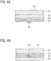
- Fig. 4A schematically shows the layer structure of the capacitive touch panel, including the cover 80.
- the cover 80 is joined to and disposed on the face of the base material 20 opposite to the face on which the sensor layer 100 is formed.
- a transparent double-sided adhesive tape or an adhesive is used to join them.
- Fig. 4A shows the first signal wire 60 formed in the jumper layer 200, as the jumper layer 200 on the insulation layer 50, and the first signal wire 60 is placed under the insulation layer 50 in this figure.
- the first signal wires 60 are wired to have an overlap with the first sensor electrodes 31 and are drawn out in the Y direction, which is the same direction in which the second signal wires 70 are drawn out. Accordingly, an area needed besides the sensor area in which the first sensor pattern 30 and the second sensor pattern 40 are placed to form a matrix is just the area along the side 21 of the base material 20 where the first signal wires 60 and the second signal wires 70 are drawn out.
- the area (wire area) other than the sensor area can be reduced by a larger amount than ever before.
- the frame of the capacitive touch panel can be narrowed, and the device size can be reduced correspondingly.
- the wire area should be provided at the side 21 of the base material 20; in other words, the wire area needs to be provided just at one side of the base material 20, and consequently, it can be easily applied not only to the conventional capacitive touch panel having a quadrilateral shape but also to capacitive touch panels having an irregular outer shape as shown in Fig. 5 .
- the first connection electrodes 32 are formed in the sensor layer 100 and the second connection electrodes 42 are formed in the jumper layer 200.
- the second connection electrodes 42 can be formed integrally with the second sensor electrodes 41 in the sensor layer 100, and the first connection electrodes 32 can be formed in the jumper layer 200.
- the sensor layer 100, the insulation layer 50, and the jumper layer 200 are laid on the base material 20 one after another in the embodiment described above, but the configuration shown in Fig. 4B can also be adopted:
- the jumper layer 200 (a first signal wire 60 formed in the jumper layer 200 is shown as the jumper layer 200 in Fig. 4B , as in Fig. 4A ) is formed first on the base material 20; then the insulation layer 50 and the sensor layer 100 are laid on them one after another. In that case, the cover 80 is placed on and joined with the sensor layer 100.
- Fig. 6 shows, in outline, the configuration of a capacitive touch panel according to a second embodiment of the present invention, and components corresponding to those in the first embodiment are indicated by identical reference characters.
- a first sensor pattern 30 and a second sensor pattern 40 are formed in different layers.
- Figs. 7A to 7C show the shapes of a lower sensor layer 110 where the first sensor pattern 30 is formed, an insulation layer 50, and an upper sensor layer 120 where the second sensor pattern 40 is formed.
- first signal wires 60 and second signal wires 70 are formed in addition to the second sensor pattern 40.
- the shapes of the first sensor pattern 30 and the second sensor pattern 40 are the same as those in the first embodiment, but the patterns are formed in different layers in this embodiment, so the holes 51 in the insulation layer 50 that are needed in the first embodiment in order to connect and conduct the second connection electrodes 42 to the second sensor electrodes 41 become unnecessary.
- the first signal wires 60 and the second signal wires 70 are drawn out in the same manner as in the first embodiment. Holes 52 are provided in the insulation layer 50 in order to connect and conduct the first signal wires 60 and the first sensor electrodes 31.
- the position and configuration of a cover 80 are not shown especially, but the cover 80 is joined to and disposed on a base material 20, as in the layer configuration shown in Fig. 4A for the first embodiment described earlier.
- the configuration of the second embodiment can be adopted instead of the configuration of the first embodiment, and the configuration of the second embodiment can produce the same advantageous effect as the first embodiment.
- Fig. 8 shows, in outline, the configuration of a capacitive touch panel according to a third embodiment of the present invention.
- the first and second sensor patterns 30, 40, the first and second signal wires 60, 70 are formed of transparent electrode films made of PEDOT, ITO or the like, but this embodiment differs from the first embodiment in that first and second sensor patterns 30, 40, first and second signal wires 60, 70 are formed by mesh patterns.
- the mesh patterns As a material forming the mesh patterns, silver, copper, carbon, or the like can be used, and the mesh patterns can be formed by printing or sputtering. Although the mesh patterns are opaque, sufficient transparency can be ensured by forming the mesh structure with fine-line patterns.
- Fig. 9 shows, in outline, the configuration of a capacitive touch panel according to a fourth embodiment of the present invention.
- This embodiment differs from the second embodiment in that first and second sensor patterns 30, 40, first and second signal wires 60, 70 are formed by mesh patterns, as in the third embodiment.
- the first and second signal wires 60, 70 can be formed by fine-line patterns placed in parallel, for example, instead of the transparent electrode films or the mesh patterns.
- a material forming the fine-line patterns silver, copper, carbon, or the like can be used, as in the mesh patterns. It is also possible that separately provided metal wires made of silver or copper are used, for example, as the first signal wires 60.
- first signal wires 60 are wired to have an overlap with the first sensor electrodes 31, stray capacitance occurring due to the electrical potential difference between them could lower the sensitivity, but if the first signal wires 60 and the first sensor electrodes 31 are formed by mesh patterns, for example, the stray capacitance would decrease, and consequently the sensitivity degradation could be reduced.
- a drive system for synchronizing drive signals for the first electrode lines 33 (X electrode lines) with one another and passing drive signals for the second electrode lines 43 (Y electrode lines) progressively is adopted.
- this type of drive system no electrical potential difference occurs between the first signal wires 60 and the first sensor electrodes 31, and consequently no stray capacitance occurs; on the other hand, stray capacitance occurs between the signal wires and the second sensor electrodes 41, but the stray capacitance is small because the first signal wires 60 are not close to the second sensor electrodes 41. Therefore, the drive system described above will hardly lower the sensitivity even if the first signal wires 60 are wired to have an overlap with the first sensor electrodes 31.
Abstract

Description
- The present invention relates to a projected capacitive touch panel.
-
Figs. 1A and 1B show a configuration included in Patent literature 1 as a conventional example of this type of capacitive touch panel, in whichfirst electrodes 12,second electrodes 13,first connection parts 14,second connection parts 15,insulation sheets 16, andlead wires 17 are formed on or above atransparent base material 11. - The
first electrodes 12 are arranged linearly in an X direction, they are coupled byfirst connection parts 14 to form a first electrode line, and first electrode lines are arranged in parallel above thetransparent base material 11. Thesecond electrodes 13 are arranged linearly in a Y direction orthogonal to the X direction, they are coupled bysecond connection parts 15 to form a second electrode line, and second electrode lines are arranged in parallel on or above thetransparent base material 11. - The first and second electrode lines are disposed to cross each other such that the
first connection parts 14 have an overlap with thesecond connection parts 15, causing a lattice of thefirst electrodes 12 and thesecond electrodes 13 to be formed above thetransparent base material 11. Theinsulation sheets 16 are placed between thefirst connection parts 14 and thesecond connection parts 15. - The
lead wires 17 are independently connected to the first and second electrode lines and are formed above thetransparent base material 11. A control circuit which is not shown in the figures is connected to thefirst electrodes 12 and thesecond electrodes 13 by thelead wires 17. - The capacitive touch panel having the configuration described above is manufactured by forming, over the
transparent base material 11, thesecond connection parts 15 and theinsulation sheets 16, and then forming thefirst electrodes 12, thesecond electrodes 13, thefirst connection parts 14, and thelead wires 17 simultaneously. Thefirst electrodes 12 and thesecond electrodes 13 are electrodes each having a mesh structure formed by a fine-line pattern. - Patent literature 1: Japanese Patent Application Laid Open No.
2014-85771 - Since the conventional projected capacitive touch panel having the configuration shown in
Figs. 1A and 1B has the lead wires 17 (signal wires) for connecting to an external circuit which are laid outside a sensor area, where the lattice of thefirst electrodes 12 and thesecond electrode 13 is placed, such that thelead wires 17 surround the sensor area, quite a wide area (wire area) is required in addition to the sensor area. The need for such a wire area prevents size reduction. - An object of the present invention is to provide a capacitive touch panel that allows the size of the area other than the sensor area to be greatly reduced, thus allowing the device to be made smaller than ever before.
- According to the present invention, a capacitive touch panel includes a first sensor pattern that includes a plurality of first electrode lines arranged in parallel, each first electrode line including a plurality of first sensor electrodes arranged in a first direction and a plurality of first connection electrodes that connect adjacent first sensor electrodes; a second sensor pattern that includes a plurality of second electrode lines arranged in parallel, each second electrode line including a plurality of second sensor electrodes arranged in a second direction that crosses the first direction and a plurality of second connection electrodes that connect adjacent second sensor electrodes, the second sensor pattern being insulated from the first sensor pattern and forming a matrix together with the first sensor pattern; first signal wires drawn out in the second direction from the first electrode lines, respectively; and second signal wires drawn out in the second direction from the second electrode lines, respectively. The first signal wires are laid overlappingly with the first sensor electrodes with an insulation layer placed therebetween, except for connection parts to the first sensor electrodes.
- According to the present invention, the area (wire area) other than the sensor area where the first sensor pattern and the second sensor pattern are placed to form a matrix can be reduced in size more greatly than ever before. Consequently the frame of the capacitive touch panel can be narrowed, and the device size can be reduced correspondingly.
-
-
Fig. 1A is a plan showing an example of a conventional capacitive touch panel;Fig. 1B is a partial enlarged view ofFig. 1A ; -
Fig. 2A is a plan showing, in outline, the configuration of a capacitive touch panel according to a first embodiment of the present invention;Fig. 2B is a partial enlarged sectional view ofFig. 2A ; -
Fig. 3A is a plan showing the shape of a sensor layer of the capacitive touch panel shown inFig. 2A ;Fig. 3B is a plan showing the shape of an insulation layer of the capacitive touch panel shown inFig. 2A ;Fig. 3C is a plan showing the shape of a jumper layer of the capacitive touch panel shown inFig. 2A ; -
Fig. 4A is a sectional view schematically showing the layer configuration of the capacitive touch panel shown inFig. 2A ;Fig. 4B is a sectional view schematically showing a different form of layer configuration of the capacitive touch panel; -
Fig. 5 is a plan showing an example obtained by changing the outer shape of the capacitive touch panel shown inFig. 2A ; -
Fig. 6 is a plan showing, in outline, the configuration of a capacitive touch panel according to a second embodiment of the present invention; -
Fig. 7A is a plan showing the shape of a lower sensor layer of the capacitive touch panel shown inFig. 6 ;Fig. 7B is a plan showing the shape of an insulation layer of the capacitive touch panel shown inFig. 6 ;Fig. 7C is a plan showing the shape of an upper sensor layer of the capacitive touch panel shown inFig. 6 ; -
Fig. 8 is a plan showing, in outline, the configuration of a capacitive touch panel according to a third embodiment of the present invention; and -
Fig. 9 is a plan view showing, in outline, the configuration of a capacitive touch panel according to a fourth embodiment of the present invention. - Embodiments of the present invention will be described.
- Components are made from transparent materials (except for some parts), and the outline of a lower layer could be seen in parts where layers are laid on one another in the plans showing the multilayer configurations, among the figures referenced below; however, the outline that could be seen actually is hidden where appropriate, in order to clearly show the vertical relationship among the layers.
-
Fig. 2A shows, in outline, the configuration of a projected capacitive touch panel according to a first embodiment of the present invention, in which afirst sensor pattern 30, asecond sensor pattern 40, aninsulation layer 50,first signal wires 60, andsecond signal wires 70 are formed on or above abase material 20. - The
first sensor pattern 30 includesfirst electrode lines 33 placed in parallel, each electrode line includingfirst sensor electrodes 31 arranged in a first direction (X direction in this embodiment) andfirst connection electrodes 32 which connect adjacentfirst sensor electrodes 31 together.
Thefirst sensor electrodes 31, except for the ones placed at both ends of thefirst electrode lines 33 in this embodiment, have a square shape, and thefirst sensor electrodes 31 placed at both ends of thefirst electrode lines 33 have a triangular shape which is a half of the square shape. Thefirst sensor electrodes 31 are arranged such that they are connected to each other at the corners thereof by thefirst connection electrodes 32. - The
second sensor pattern 40 includessecond electrode lines 43 placed in parallel, each electrode line includingsecond sensor electrodes 41 arranged in a second direction (Y direction orthogonal to the X direction in this embodiment) which crosses the first direction andsecond connection electrodes 42 which connect adjacentsecond sensor electrodes 41 together. Like thefirst sensor electrodes 31, thesecond sensor electrodes 41 placed at both ends of thesecond electrode lines 43 have a triangular shape, and the ones not placed at both ends have a square shape, and they are connected to each other at the corners thereof by thesecond connection electrodes 42. - The
first sensor pattern 30 and thesecond sensor pattern 40 are placed such that thefirst connection electrodes 32 cross each other to have an overlap with thesecond connection electrodes 42, and consequently thefirst sensor pattern 30 and thesecond sensor pattern 40 form a matrix. Thefirst sensor electrodes 31 and thesecond sensor electrodes 41 have a uniform gap between their sides that face each other in parallel. - The
first sensor electrodes 31, thesecond sensor electrodes 41, and thefirst connection electrodes 32 are formed in the same layer in this embodiment, and thesecond connection electrodes 42, which cross thefirst connection electrodes 32, are formed in a different layer. Therefore, thefirst sensor pattern 30 and thesecond sensor pattern 40 are insulated from each other. -
Fig. 2B shows the structure of a part where thefirst connection electrode 32 and thesecond connection electrode 42 cross each other. Theinsulation layer 50 placed between them causes thefirst connection electrode 32 and thesecond connection electrode 42 to be separated and insulated from each other. Both ends of thesecond connection electrode 42 are connected and conducted to thesecond sensor electrodes 41 to be connected, throughholes 51 disposed in theinsulation layer 50. - The
first sensor pattern 30 and thesecond sensor pattern 40 are connected to an external circuit (not shown in the figures) via thefirst signal wires 60 and thesecond signal wires 70, respectively. Thesecond signal wires 70 are drawn out from one end of thesecond electrode lines 43 and are laid in the Y direction, and tips are placed side by side on oneside 21 of thebase material 20. Thesecond signal wires 70 are formed in the same layer as thesecond sensor electrodes 41. - Like the
second signal wires 70, thefirst signal wires 60 are drawn out from thefirst electrode lines 33 and are laid in the Y direction, and tips are placed side by side on theside 21 of thebase material 20, like the tips of thesecond signal wires 70. As shown inFig. 2A , thefirst signal wires 60 are laid above thefirst sensor electrodes 31 with theinsulation layer 50 placed between them to separate thefirst sensor electrodes 31, except for the connection parts to thefirst sensor electrodes 31. - The inner end (connection part to the first sensor electrode 31) of each
first signal wire 60 is connected and conducted, through ahole 52 disposed in theinsulation layer 50, to a correspondingfirst sensor electrode 31. In this embodiment, fourfirst electrode lines 33 and fourholes 52 are formed: In the figure, thehole 52 for the first one of thefirst electrode lines 33 is formed on the leftmost one of thefirst sensor electrodes 31; thehole 52 for the second one of thefirst electrode lines 33 is formed on the second one from the left of thefirst sensor electrodes 31; thehole 52 for the third one of thefirst electrode lines 33 is formed on the third one from the left of thefirst sensor electrodes 31; and thehole 52 for the fourth one of thefirst electrode lines 33 is formed on the fourth one from the left of thefirst sensor electrodes 31. By forming theseholes 52 and wiring thefirst signal wires 60 above thefirst sensor electrodes 31, thefirst signal wires 60 and thesecond signal wires 70 are arranged alternately in parallel in the Y direction as shown inFig. 2A , and the pitches among them can be made uniform. - The
first signal wires 60 and thesecond connection electrodes 42 are formed in the same layer. In this embodiment, the following three layers are formed on or above thebase material 20 to configure the components described above. - (1)
Sensor layer 100 ···
first andsecond sensor electrodes
first connection electrodes 32, andsecond signal wires 70 - (2)
Insulation layer 50 - (3)
Jumper layer 200 ···
second connection electrodes 42 andfirst signal wires 60 -
Figs. 3A to 3C show the shapes (patterns) of thesensor layer 100, theinsulation layer 50, and thejumper layer 200, which are laid one after another on thebase material 20. - The
insulation layer 50 covers entire surface of thebase material 20, except for theside 21 of thebase material 20, and has theholes 51 for thesecond connection electrodes 42 and theholes 52 for thefirst signal wires 60. By removing theinsulation layer 50 on theside 21 of thebase material 20, the tips of thesecond signal wires 70 are not covered by theinsulation layer 50 and are exposed. - In the configuration described above, the
base material 20, thesensor layer 100, theinsulation layer 50, and thejumper layer 200 are all formed of transparent materials. Glass or a film can be used as thebase material 20. Thesensor layer 100 and thejumper layer 200 where the first andsecond sensor patterns second signal wires insulation layer 50 is formed of acrylic, polyimide (PI), urethane, or the like. - The
insulation layer 50 is formed to cover almost the entire surface of thebase material 20, but this type of formation is not necessarily required, and it can be formed partially where it is required. Especially when theinsulation layer 50 is formed of a resin and when the jumper layer 200 (or thejumper layer 200 and the sensor layer 100) is formed by sputtering ITO, it is preferred in terms of thermal resistance and outgassing that theinsulation layer 50 be formed partially to minimize the area of theinsulation layer 50. - A transparent cover forming a touch surface is disposed on the surface of the capacitive touch panel. The cover is formed of glass or a plastic.
-
Fig. 4A schematically shows the layer structure of the capacitive touch panel, including thecover 80. Thecover 80 is joined to and disposed on the face of thebase material 20 opposite to the face on which thesensor layer 100 is formed. A transparent double-sided adhesive tape or an adhesive is used to join them.Fig. 4A shows thefirst signal wire 60 formed in thejumper layer 200, as thejumper layer 200 on theinsulation layer 50, and thefirst signal wire 60 is placed under theinsulation layer 50 in this figure. - The configuration of the capacitive touch panel according to the first embodiment of the present invention has been described above. In this embodiment, the
first signal wires 60 are wired to have an overlap with thefirst sensor electrodes 31 and are drawn out in the Y direction, which is the same direction in which thesecond signal wires 70 are drawn out. Accordingly, an area needed besides the sensor area in which thefirst sensor pattern 30 and thesecond sensor pattern 40 are placed to form a matrix is just the area along theside 21 of thebase material 20 where thefirst signal wires 60 and thesecond signal wires 70 are drawn out. The area (wire area) other than the sensor area can be reduced by a larger amount than ever before. Therefore, in this embodiment, since the wire area can be reduced, the frame of the capacitive touch panel can be narrowed, and the device size can be reduced correspondingly. The wire area should be provided at theside 21 of thebase material 20; in other words, the wire area needs to be provided just at one side of thebase material 20, and consequently, it can be easily applied not only to the conventional capacitive touch panel having a quadrilateral shape but also to capacitive touch panels having an irregular outer shape as shown inFig. 5 . - In the embodiment described above, the
first connection electrodes 32 are formed in thesensor layer 100 and thesecond connection electrodes 42 are formed in thejumper layer 200. Conversely, thesecond connection electrodes 42 can be formed integrally with thesecond sensor electrodes 41 in thesensor layer 100, and thefirst connection electrodes 32 can be formed in thejumper layer 200. - The
sensor layer 100, theinsulation layer 50, and thejumper layer 200 are laid on thebase material 20 one after another in the embodiment described above, but the configuration shown inFig. 4B can also be adopted: The jumper layer 200 (afirst signal wire 60 formed in thejumper layer 200 is shown as thejumper layer 200 inFig. 4B , as inFig. 4A ) is formed first on thebase material 20; then theinsulation layer 50 and thesensor layer 100 are laid on them one after another. In that case, thecover 80 is placed on and joined with thesensor layer 100. - If the layer configuration shown in
Fig. 4A or Fig. 4B is adopted, thecover 80, that is, atouch surface 81 to be touched for operation, is placed, with respect to thefirst sensor electrodes 31, on the side opposite to the side on which thefirst signal wires 60 are placed, and thefirst sensor electrodes 31 function as a shield against thefirst signal wires 60 when viewed from thetouch surface 81. This shielding effect of thefirst sensor electrodes 31 can prevent a malfunction from occurring caused by a change in capacitance between thefirst signal wires 60 and thetouch surface 81. -
Fig. 6 shows, in outline, the configuration of a capacitive touch panel according to a second embodiment of the present invention, and components corresponding to those in the first embodiment are indicated by identical reference characters. - In this embodiment, a
first sensor pattern 30 and asecond sensor pattern 40 are formed in different layers.Figs. 7A to 7C show the shapes of alower sensor layer 110 where thefirst sensor pattern 30 is formed, aninsulation layer 50, and anupper sensor layer 120 where thesecond sensor pattern 40 is formed. In theupper sensor layer 120,first signal wires 60 andsecond signal wires 70 are formed in addition to thesecond sensor pattern 40. - The shapes of the
first sensor pattern 30 and thesecond sensor pattern 40 are the same as those in the first embodiment, but the patterns are formed in different layers in this embodiment, so theholes 51 in theinsulation layer 50 that are needed in the first embodiment in order to connect and conduct thesecond connection electrodes 42 to thesecond sensor electrodes 41 become unnecessary. - The
first signal wires 60 and thesecond signal wires 70 are drawn out in the same manner as in the first embodiment.Holes 52 are provided in theinsulation layer 50 in order to connect and conduct thefirst signal wires 60 and thefirst sensor electrodes 31. The position and configuration of acover 80 are not shown especially, but thecover 80 is joined to and disposed on abase material 20, as in the layer configuration shown inFig. 4A for the first embodiment described earlier. - The configuration of the second embodiment can be adopted instead of the configuration of the first embodiment, and the configuration of the second embodiment can produce the same advantageous effect as the first embodiment.
-
Fig. 8 shows, in outline, the configuration of a capacitive touch panel according to a third embodiment of the present invention. - In the first and second embodiments, the first and
second sensor patterns second signal wires second sensor patterns second signal wires - As a material forming the mesh patterns, silver, copper, carbon, or the like can be used, and the mesh patterns can be formed by printing or sputtering. Although the mesh patterns are opaque, sufficient transparency can be ensured by forming the mesh structure with fine-line patterns.
-
Fig. 9 shows, in outline, the configuration of a capacitive touch panel according to a fourth embodiment of the present invention. This embodiment differs from the second embodiment in that first andsecond sensor patterns second signal wires - In the embodiments described above, the first and
second signal wires first signal wires 60. - Since the
first signal wires 60 are wired to have an overlap with thefirst sensor electrodes 31, stray capacitance occurring due to the electrical potential difference between them could lower the sensitivity, but if thefirst signal wires 60 and thefirst sensor electrodes 31 are formed by mesh patterns, for example, the stray capacitance would decrease, and consequently the sensitivity degradation could be reduced. - Generally, a drive system for synchronizing drive signals for the first electrode lines 33 (X electrode lines) with one another and passing drive signals for the second electrode lines 43 (Y electrode lines) progressively is adopted. With this type of drive system, no electrical potential difference occurs between the
first signal wires 60 and thefirst sensor electrodes 31, and consequently no stray capacitance occurs; on the other hand, stray capacitance occurs between the signal wires and thesecond sensor electrodes 41, but the stray capacitance is small because thefirst signal wires 60 are not close to thesecond sensor electrodes 41. Therefore, the drive system described above will hardly lower the sensitivity even if thefirst signal wires 60 are wired to have an overlap with thefirst sensor electrodes 31.
Claims (10)
- A capacitive touch panel comprising:a first sensor pattern comprising first electrode lines arranged in parallel, each first electrode line comprising first sensor electrodes arranged in a first direction and first connection electrodes that connect adjacent first sensor electrodes;a second sensor pattern comprising second electrode lines arranged in parallel, each second electrode line comprising second sensor electrodes arranged in a second direction that crosses the first direction and second connection electrodes that connect adjacent second sensor electrodes, the second sensor pattern being insulated from the first sensor pattern and forming a matrix together with the first sensor pattern;first signal wires drawn out in the second direction from the first electrode lines, the first signal wires being wired to have an overlap with the first sensor electrodes with an insulation layer placed therebetween, except for connection parts to the first sensor electrodes; andsecond signal wires drawn out in the second direction from the second electrode lines.
- The capacitive touch panel according to Claim 1, wherein the first sensor electrodes and the second sensor electrodes are formed in a layer; and
the first signal wires are formed in a layer differing from the layer of the first and second sensor electrodes. - The capacitive touch panel according to Claim 2, wherein either the first connection electrodes or the second connection electrodes is formed in the layer of the first and second sensor electrodes, and other connection electrodes are formed in the layer of the first signal wires.
- The capacitive touch panel according to Claim 1, wherein the first sensor pattern is formed in a layer different from a layer of the second sensor pattern; and
the first signal wires are formed in the layer of the second sensor pattern. - The capacitive touch panel according to one of Claims 1 to 4, wherein the first and second sensor patterns are formed by mesh patterns.
- The capacitive touch panel according to one of Claims 1 to 5, wherein the first signal wires are formed by mesh patterns.
- The capacitive touch panel according to one of Claims 1 to 5, wherein the first signal wires are formed by fine-line patterns.
- The capacitive touch panel according to one of Claims 1 to 4, wherein the first and second sensor patterns and the first signal wires are formed of a transparent material.
- The capacitive touch panel according to one of Claims 1 to 8, wherein a touch surface to be touched for operation is placed, with respect to the first sensor electrodes, on a side opposite to a side where the first signal wires are placed.
- The capacitive touch panel according to one of Claims 1 to 9, wherein the outer shape is not quadrilateral.
Applications Claiming Priority (2)
| Application Number | Priority Date | Filing Date | Title |
|---|---|---|---|
| JP2014169134A JP5813836B1 (en) | 2014-08-22 | 2014-08-22 | Capacitive touch panel |
| PCT/JP2015/066823 WO2016027555A1 (en) | 2014-08-22 | 2015-06-11 | Electrostatic capacitance touch panel |
Publications (2)
| Publication Number | Publication Date |
|---|---|
| EP3156887A1 true EP3156887A1 (en) | 2017-04-19 |
| EP3156887A4 EP3156887A4 (en) | 2018-01-03 |
Family
ID=54595867
Family Applications (1)
| Application Number | Title | Priority Date | Filing Date |
|---|---|---|---|
| EP15834462.2A Withdrawn EP3156887A4 (en) | 2014-08-22 | 2015-06-11 | Electrostatic capacitance touch panel |
Country Status (5)
| Country | Link |
|---|---|
| US (1) | US20170255296A1 (en) |
| EP (1) | EP3156887A4 (en) |
| JP (1) | JP5813836B1 (en) |
| CN (1) | CN106537304A (en) |
| WO (1) | WO2016027555A1 (en) |
Families Citing this family (6)
| Publication number | Priority date | Publication date | Assignee | Title |
|---|---|---|---|---|
| KR20160114510A (en) * | 2015-03-24 | 2016-10-05 | 가부시키가이샤 한도오따이 에네루기 켄큐쇼 | Touch panel |
| KR101980728B1 (en) * | 2015-07-14 | 2019-05-21 | 주식회사 엘지화학 | Conductive structure body, method for manufacturing thereof, touch panel comprising thereof and display device comprising thereof |
| TWI746615B (en) * | 2016-08-18 | 2021-11-21 | 日商住友化學股份有限公司 | Method for manufacturing polarizing film, manufacturing apparatus and polarizing film |
| JP7030447B2 (en) * | 2016-08-18 | 2022-03-07 | 住友化学株式会社 | Method and equipment for manufacturing polarizing film |
| JP2020173693A (en) * | 2019-04-12 | 2020-10-22 | 株式会社ピクトリープ | Touch sensor |
| KR20220093784A (en) * | 2020-12-28 | 2022-07-05 | 엘지디스플레이 주식회사 | Touch display device |
Family Cites Families (7)
| Publication number | Priority date | Publication date | Assignee | Title |
|---|---|---|---|---|
| CN101681223A (en) * | 2007-05-07 | 2010-03-24 | 爱特梅尔公司 | Two-dimensional position sensor |
| KR101329638B1 (en) * | 2008-07-31 | 2013-11-14 | 군제 가부시키가이샤 | Planar element, and touch switch |
| US20120018198A1 (en) * | 2010-03-30 | 2012-01-26 | Ibiden Co., Ltd. | Electronic component and printed wiring board |
| KR101663210B1 (en) * | 2010-04-28 | 2016-10-06 | 주식회사 동진쎄미켐 | Touch panel and method for manufacturing the same |
| KR101793677B1 (en) * | 2011-01-18 | 2017-11-06 | 삼성디스플레이 주식회사 | Touch Screen Panel |
| CN103472963B (en) * | 2013-09-06 | 2016-05-11 | 北京京东方光电科技有限公司 | A kind of touching display screen and touch control display apparatus |
| JP6327925B2 (en) * | 2014-04-30 | 2018-05-23 | 株式会社ワコム | Position detection device |
-
2014
- 2014-08-22 JP JP2014169134A patent/JP5813836B1/en active Active
-
2015
- 2015-06-11 US US15/320,336 patent/US20170255296A1/en not_active Abandoned
- 2015-06-11 CN CN201580037884.0A patent/CN106537304A/en active Pending
- 2015-06-11 EP EP15834462.2A patent/EP3156887A4/en not_active Withdrawn
- 2015-06-11 WO PCT/JP2015/066823 patent/WO2016027555A1/en active Application Filing
Also Published As
| Publication number | Publication date |
|---|---|
| JP2016045684A (en) | 2016-04-04 |
| WO2016027555A1 (en) | 2016-02-25 |
| JP5813836B1 (en) | 2015-11-17 |
| EP3156887A4 (en) | 2018-01-03 |
| US20170255296A1 (en) | 2017-09-07 |
| CN106537304A (en) | 2017-03-22 |
Similar Documents
| Publication | Publication Date | Title |
|---|---|---|
| EP3156887A1 (en) | Electrostatic capacitance touch panel | |
| US10152181B2 (en) | Touch display device and driving method thereof | |
| JP6220985B2 (en) | Laminated structure, touch panel, display device with touch panel, and manufacturing method thereof | |
| US10133380B2 (en) | Touch display device and driving method thereof | |
| US10042493B2 (en) | Touch panel having inconspicuous electrodes | |
| CN106020557B (en) | Touch display panel, driving method and touch display device | |
| US9582129B2 (en) | Touch screen panel | |
| CN107037909B (en) | Touch detection device and display device with touch detection function | |
| CN105094482A (en) | OGS capacitive touch screen and preparing method thereof | |
| TWI798278B (en) | Touch panel and display device comprising same | |
| US10013928B2 (en) | Touch panel | |
| KR102394537B1 (en) | Capacitive touch panel | |
| KR20160057572A (en) | Touch Screen Panel | |
| US11314362B2 (en) | Touch substrate, touch control display apparatus, method of fabricating touch substrate | |
| CN106155411A (en) | Touch screen, touch panel, display device and electronic equipment | |
| TW201519031A (en) | Touch panel and touch display panel | |
| JP7007258B2 (en) | Touch screen, display device and touch panel | |
| CN110275650B (en) | Touch sensing device, touch display panel and touch display panel mother board | |
| CN104714680A (en) | Touch control panel | |
| JP2017004519A (en) | Conductive pattern substrate | |
| US10521057B2 (en) | Touch screen panel having overlapping sensing electrodes and method of manufacturing the same | |
| CN111367438A (en) | Display panel and display device | |
| JP6747084B2 (en) | Conductive pattern substrate and display device with touch position detection function | |
| JP3183604U (en) | Bridge structure of signal transmission cable for touchpad | |
| JP2022133487A (en) | Transparent electrode member, capacitive sensor, and input and output apparatus |
Legal Events
| Date | Code | Title | Description |
|---|---|---|---|
| PUAI | Public reference made under article 153(3) epc to a published international application that has entered the european phase |
Free format text: ORIGINAL CODE: 0009012 |
|
| 17P | Request for examination filed |
Effective date: 20170110 |
|
| AK | Designated contracting states |
Kind code of ref document: A1 Designated state(s): AL AT BE BG CH CY CZ DE DK EE ES FI FR GB GR HR HU IE IS IT LI LT LU LV MC MK MT NL NO PL PT RO RS SE SI SK SM TR |
|
| AX | Request for extension of the european patent |
Extension state: BA ME |
|
| DAV | Request for validation of the european patent (deleted) | ||
| DAX | Request for extension of the european patent (deleted) | ||
| A4 | Supplementary search report drawn up and despatched |
Effective date: 20171201 |
|
| RIC1 | Information provided on ipc code assigned before grant |
Ipc: G06F 3/044 20060101ALI20171127BHEP Ipc: G06F 3/041 20060101AFI20171127BHEP |
|
| 17Q | First examination report despatched |
Effective date: 20180928 |
|
| STAA | Information on the status of an ep patent application or granted ep patent |
Free format text: STATUS: THE APPLICATION HAS BEEN WITHDRAWN |
|
| 18W | Application withdrawn |
Effective date: 20190206 |