EP3153919A1 - Grating base plate and manufacturing method therefor, and display device - Google Patents
Grating base plate and manufacturing method therefor, and display device Download PDFInfo
- Publication number
- EP3153919A1 EP3153919A1 EP14861122.1A EP14861122A EP3153919A1 EP 3153919 A1 EP3153919 A1 EP 3153919A1 EP 14861122 A EP14861122 A EP 14861122A EP 3153919 A1 EP3153919 A1 EP 3153919A1
- Authority
- EP
- European Patent Office
- Prior art keywords
- conductive bridges
- touch electrodes
- forming
- array
- base substrate
- Prior art date
- Legal status (The legal status is an assumption and is not a legal conclusion. Google has not performed a legal analysis and makes no representation as to the accuracy of the status listed.)
- Granted
Links
Images


Classifications
-
- G—PHYSICS
- G06—COMPUTING OR CALCULATING; COUNTING
- G06F—ELECTRIC DIGITAL DATA PROCESSING
- G06F3/00—Input arrangements for transferring data to be processed into a form capable of being handled by the computer; Output arrangements for transferring data from processing unit to output unit, e.g. interface arrangements
- G06F3/01—Input arrangements or combined input and output arrangements for interaction between user and computer
- G06F3/03—Arrangements for converting the position or the displacement of a member into a coded form
- G06F3/041—Digitisers, e.g. for touch screens or touch pads, characterised by the transducing means
- G06F3/0412—Digitisers structurally integrated in a display
-
- G—PHYSICS
- G02—OPTICS
- G02B—OPTICAL ELEMENTS, SYSTEMS OR APPARATUS
- G02B27/00—Optical systems or apparatus not provided for by any of the groups G02B1/00 - G02B26/00, G02B30/00
- G02B27/10—Beam splitting or combining systems
- G02B27/1086—Beam splitting or combining systems operating by diffraction only
-
- G—PHYSICS
- G02—OPTICS
- G02B—OPTICAL ELEMENTS, SYSTEMS OR APPARATUS
- G02B30/00—Optical systems or apparatus for producing three-dimensional [3D] effects, e.g. stereoscopic images
- G02B30/20—Optical systems or apparatus for producing three-dimensional [3D] effects, e.g. stereoscopic images by providing first and second parallax images to an observer's left and right eyes
- G02B30/22—Optical systems or apparatus for producing three-dimensional [3D] effects, e.g. stereoscopic images by providing first and second parallax images to an observer's left and right eyes of the stereoscopic type
- G02B30/25—Optical systems or apparatus for producing three-dimensional [3D] effects, e.g. stereoscopic images by providing first and second parallax images to an observer's left and right eyes of the stereoscopic type using polarisation techniques
-
- G—PHYSICS
- G02—OPTICS
- G02B—OPTICAL ELEMENTS, SYSTEMS OR APPARATUS
- G02B30/00—Optical systems or apparatus for producing three-dimensional [3D] effects, e.g. stereoscopic images
- G02B30/20—Optical systems or apparatus for producing three-dimensional [3D] effects, e.g. stereoscopic images by providing first and second parallax images to an observer's left and right eyes
- G02B30/26—Optical systems or apparatus for producing three-dimensional [3D] effects, e.g. stereoscopic images by providing first and second parallax images to an observer's left and right eyes of the autostereoscopic type
- G02B30/27—Optical systems or apparatus for producing three-dimensional [3D] effects, e.g. stereoscopic images by providing first and second parallax images to an observer's left and right eyes of the autostereoscopic type involving lenticular arrays
-
- G—PHYSICS
- G02—OPTICS
- G02B—OPTICAL ELEMENTS, SYSTEMS OR APPARATUS
- G02B30/00—Optical systems or apparatus for producing three-dimensional [3D] effects, e.g. stereoscopic images
- G02B30/20—Optical systems or apparatus for producing three-dimensional [3D] effects, e.g. stereoscopic images by providing first and second parallax images to an observer's left and right eyes
- G02B30/26—Optical systems or apparatus for producing three-dimensional [3D] effects, e.g. stereoscopic images by providing first and second parallax images to an observer's left and right eyes of the autostereoscopic type
- G02B30/30—Optical systems or apparatus for producing three-dimensional [3D] effects, e.g. stereoscopic images by providing first and second parallax images to an observer's left and right eyes of the autostereoscopic type involving parallax barriers
-
- G—PHYSICS
- G02—OPTICS
- G02B—OPTICAL ELEMENTS, SYSTEMS OR APPARATUS
- G02B5/00—Optical elements other than lenses
- G02B5/18—Diffraction gratings
- G02B5/1847—Manufacturing methods
- G02B5/1857—Manufacturing methods using exposure or etching means, e.g. holography, photolithography, exposure to electron or ion beams
-
- G—PHYSICS
- G02—OPTICS
- G02F—OPTICAL DEVICES OR ARRANGEMENTS FOR THE CONTROL OF LIGHT BY MODIFICATION OF THE OPTICAL PROPERTIES OF THE MEDIA OF THE ELEMENTS INVOLVED THEREIN; NON-LINEAR OPTICS; FREQUENCY-CHANGING OF LIGHT; OPTICAL LOGIC ELEMENTS; OPTICAL ANALOGUE/DIGITAL CONVERTERS
- G02F1/00—Devices or arrangements for the control of the intensity, colour, phase, polarisation or direction of light arriving from an independent light source, e.g. switching, gating or modulating; Non-linear optics
- G02F1/01—Devices or arrangements for the control of the intensity, colour, phase, polarisation or direction of light arriving from an independent light source, e.g. switching, gating or modulating; Non-linear optics for the control of the intensity, phase, polarisation or colour
- G02F1/13—Devices or arrangements for the control of the intensity, colour, phase, polarisation or direction of light arriving from an independent light source, e.g. switching, gating or modulating; Non-linear optics for the control of the intensity, phase, polarisation or colour based on liquid crystals, e.g. single liquid crystal display cells
- G02F1/133—Constructional arrangements; Operation of liquid crystal cells; Circuit arrangements
- G02F1/1333—Constructional arrangements; Manufacturing methods
- G02F1/1343—Electrodes
-
- H—ELECTRICITY
- H04—ELECTRIC COMMUNICATION TECHNIQUE
- H04N—PICTORIAL COMMUNICATION, e.g. TELEVISION
- H04N13/00—Stereoscopic video systems; Multi-view video systems; Details thereof
- H04N13/30—Image reproducers
- H04N13/302—Image reproducers for viewing without the aid of special glasses, i.e. using autostereoscopic displays
- H04N13/31—Image reproducers for viewing without the aid of special glasses, i.e. using autostereoscopic displays using parallax barriers
-
- G—PHYSICS
- G06—COMPUTING OR CALCULATING; COUNTING
- G06F—ELECTRIC DIGITAL DATA PROCESSING
- G06F2203/00—Indexing scheme relating to G06F3/00 - G06F3/048
- G06F2203/041—Indexing scheme relating to G06F3/041 - G06F3/045
- G06F2203/04103—Manufacturing, i.e. details related to manufacturing processes specially suited for touch sensitive devices
-
- G—PHYSICS
- G06—COMPUTING OR CALCULATING; COUNTING
- G06F—ELECTRIC DIGITAL DATA PROCESSING
- G06F2203/00—Indexing scheme relating to G06F3/00 - G06F3/048
- G06F2203/041—Indexing scheme relating to G06F3/041 - G06F3/045
- G06F2203/04111—Cross over in capacitive digitiser, i.e. details of structures for connecting electrodes of the sensing pattern where the connections cross each other, e.g. bridge structures comprising an insulating layer, or vias through substrate
Definitions
- Embodiments of the invention relate to a grating substrate, a fabrication method thereof and a display device.
- a touch screen is the most simple, convenient and natural way of man-machine interaction at present.
- a number of first touch electrodes and a number of second touch electrodes in an array are formed to connect different signals so as to detect a touch point.
- a parallax barrier 3D display technology is a kind of naked-eye type 3D display technologies without wearing a 3D glasses, and its main structure includes: a display and a slit grating arranged on a light emitting side of the display.
- a display and a slit grating arranged on a light emitting side of the display.
- Embodiments of the present invention provide a grating substrate and a fabrication method thereof, and a display device, which can achieve both a touch function and a 3D light-splitting function at the same time.
- an embodiment of the present invention provides a fabrication method of a grating substrate, comprising: forming an array of comb-shaped, opaque touch electrodes and a plurality of first conductive bridges on a base substrate, wherein the array of touch electrodes comprises a plurality of first touch electrodes and a plurality of second touch electrodes which are disconnected from each other, and the plurality of first touch electrodes in the array are connected to each other by the first conductive bridges; forming an insulating spacing layer on the base substrate on which the array of the touch electrodes and the plurality of first conductive bridges are formed, the insulating spacing layer covering the first conductive bridges; and forming second conductive bridges on the insulating spacing layer, the plurality of second touch electrodes in the array being connected to each other by the second conductive bridges.
- an embodiment of the present invention further provides a fabrication method of a grating substrate, comprising: forming second conductive bridges on predetermined positions on a base substrate; forming an insulating spacing layer on the base substrate on which the second conductive bridges are formed, to make the insulating spacing layer cover the second conductive bridges; forming an array of comb-shaped, opaque touch electrodes and a plurality of first conductive bridges on the base substrate on which the second conductive bridges and the insulating spacing layer are formed, wherein the array of touch electrodes comprises a plurality of first touch electrodes and a plurality of second touch electrodes which are disconnected from each other, and the plurality of first touch electrodes in the array are connected to each other by the first conductive bridges, while the plurality of second touch electrodes in the array are connected to each other by the second conductive bridges, and the insulating spacing layer is arranged between the first conductive bridges and the second conductive bridges.
- an embodiment of the present invention further provides a grating substrate, comprising: a plurality of first conductive bridges, a plurality of comb-shaped, opaque first touch electrodes, and a plurality of comb-shaped, opaque second touch electrodes, formed in a same layer on a base substrate; a plurality of second conductive bridges, configured to connect the plurality of second touch electrodes, wherein the plurality of first touch electrodes are not connected to the plurality of second touch electrodes, the plurality of first conductive bridges are configured to connect the plurality of first touch electrodes, and an insulating spacing layer is arranged between the first conductive bridges and the second conductive bridges.
- an embodiment of the present invention further provides a display device, comprising the grating substrate described above.
- the opaque touch electrode may be a metal electrode.
- the touch electrode is made to be an opaque comb-shaped electrode, so that the touch electrode can be used as not only a touch electrode of a touch screen but also an electrode of a 3D slit grating, so as to achieve both a touch function and a 3D light-splitting function at the same time.
- FIGs. 1-3 Exemplarily, an exemplary description of the fabrication method of the grating substrate is given with reference to FIGs. 1-3 ; for simplicity, only four touch electrodes are shown in FIGs. 1-3 , and more touch electrodes are not shown.
- a first conductive bridge 3 is made of the same material with the touch electrode, so while an array of comb-shaped, opaque touch electrodes (including a plurality of first touch electrodes 1 and a plurality of second touch electrodes 2) is formed on the base substrate, the first conductive bridge 3 is formed too, and the first conductive bridge 3 is used to connect a plurality of first touch electrodes 1.
- the first conductive bridge 3 and the touch electrodes may be fabricated by using a patterning process (the patterning process generally includes coating a photoresist, exposing, developing, etching, removing the photoresist and so on).
- an insulating spacing layer 4 covering the first conductive bridge 3 may cover the entire base substrate (when it covers the entire base substrate, through holes are formed in regions of the insulating spacing layer corresponding to regions where the second touch electrode and the second conductive bridge are connected), or may only cover a region where the first conductive bridge is formed, or may only cover an overlapping region between the second conductive bridge to be formed and the first conductive bridge.
- the final grating substrate is shown in FIG. 3 , and in the embodiment, the insulating spacing layer 4 is shown to only cover the overlapping region between the second conductive bridge to be formed and the first conductive bridge, to save material.
- a layer of photoresist may be formed at first, and the photoresist in the region where the insulating spacing layer 4 is to be formed is removed, then a layer of insulating spacing material is formed, and finally the photoresist is removed, so that the insulating spacing material covered the photoresist is removed altogether, to finally form the insulating spacing layer 4.
- step 3 when a second conductive bridge is formed, a layer of photoresist may be formed at first, and the photoresist in the region where the second conductive bridge is to be formed is removed, then a layer of conductive material (e.g., metal) is formed, and finally the photoresist is removed, so that the conductive material covered the photoresist is removed altogether, to finally form a second conductive bridge 5 to connect with the second touch electrode 2.
- a layer of photoresist may be formed at first, and the photoresist in the region where the second conductive bridge is to be formed is removed, then a layer of conductive material (e.g., metal) is formed, and finally the photoresist is removed, so that the conductive material covered the photoresist is removed altogether, to finally form a second conductive bridge 5 to connect with the second touch electrode 2.
- a layer of photoresist may be formed at first, and the photoresist in the region where the second conductive bridge is to be formed is removed, then a layer
- a protective layer may be formed to protect the grating substrate.
- the base substrate may be a color filter (CF) substrate, and a plurality of touch electrodes and the first and second conductive bridges may be formed on a side of the base substrate opposite to a color filter, so that no additional grating alignment is needed when the slit grating is attached to the display panel, thus avoiding the alignment deviation.
- CF color filter
- the base substrate may also be formed inside the protective layer (Cover).
- connection bar for connecting comb teeth corresponds to a black matrix of the base substrate.
- a layer of photoresist may be formed at first, and the photoresist in the region where the second conductive bridge is to be formed is removed, then a layer of conductive material (e.g., metal) is formed, and finally the photoresist is removed, so that the conductive material covered the photoresist is removed altogether, to finally form the second conductive bridge; or a layer of conductive material is formed at first, and then fabrication is performed by a patterning process (the patterning process generally includes coating photoresist, exposing, developing, etching, removing the photoresist and so on).
- the patterning process generally includes coating photoresist, exposing, developing, etching, removing the photoresist and so on).
- the insulating spacing layer covering the second conductive bridge may cover the entire base substrate (when it covers the entire base substrate, through holes are formed in the insulating spacing layer corresponding to regions where the second touch electrode and the second conductive bridge are connected), or may only cover a region where the second conductive bridge is formed, or may only cover an overlapping region between the first conductive bridge to be formed and the second conductive bridge.
- the first conductive bridge is made of the same material with the touch electrode, so while an array of comb-shaped, opaque touch electrodes (including the first touch electrodes and the second touch electrodes) is formed on the base substrate, the first conductive bridge is formed too, to connect the first touch electrodes.
- the first conductive bridge 3 and the touch electrodes may be fabricated by a patterning process (the patterning process generally includes coating a photoresist, exposing, developing, etching, removing the photoresist and so on). Meanwhile the second conductive bridge formed in step 1 is used to connect the second touch electrodes of the array together, and the first conductive bridge and the second conductive bridge is spaced by the insulating spacing layer.
- a protection layer may be formed to protect the grating substrate.
- the base substrate may be a color filter (CF) substrate, and a plurality of touch electrodes and the first and second conductive bridges may be formed on a side of the base substrate opposite to a color filter, so that no additional grating alignment is needed when the slit grating is attached to the display panel, thus avoiding an alignment deviation.
- CF color filter
- the base substrate may also be formed inside the protective layer (Cover).
- connection bar for connecting comb teeth is located in a region corresponding to a black matrix of the base substrate.
- the embodiment of the invention further provides a grating substrate, comprising: a plurality of first conductive bridges, a plurality of comb-shaped, opaque first touch electrodes, and a plurality of comb-shaped, opaque second touch electrodes, formed in a same layer of a base substrate; a plurality of second conductive bridges, configured to connect the plurality of second touch electrodes, wherein the plurality of first touch electrodes are not connected to the plurality of second touch electrodes, and the plurality of first conductive bridges are configured to connect the plurality of first touch electrodes, and an insulating spacing layer is arranged between the first conductive bridges and the second conductive bridges.
- Each of the first touch electrodes and the second touch electrodes is a comb-shaped electrode.
- the base substrate is a color filter (CF) substrate, or for One Glass Solution (OGS), it may also be formed inside a protection layer (Cover).
- CF color filter
- OGS One Glass Solution
- connection bar for connecting comb teeth is located in a region corresponding to a black matrix of the base substrate.
- the insulating spacing layer is only formed in overlapping regions of the first conductive bridges and the second conductive bridges.
- the insulating spacing layer covers the entire base substrate, in which a plurality of through holes are formed to connect the plurality of second touch electrodes and the second conductive bridges.
- the plurality of first conductive bridges, the plurality of comb-shaped, opaque first touch electrodes, and the plurality of comb-shaped, opaque second touch electrodes are made from same material.
- the touch electrode is an opaque comb-shaped electrode, which can be used as not only a touch electrode of a touch screen but also an electrode of a 3D slit grating, to achieve both a touch function and a 3D light-splitting function at the same time.
- An embodiment of the present invention further provides a display device, comprising a display panel and the grating substrate mentioned above disposed on a light outgoing side of the display panel.
- the display panel may be a liquid crystal display panel, including: an array substrate; a color filter substrate, disposed opposite to the array substrate; and a liquid crystal layer, disposed between the array substrate and the color filter substrate, wherein the base substrate of the grating substrate is the color filter substrate, wherein the plurality of touch electrodes and the first and second conductive bridges may be formed on a side of base substrate opposite to a color filter.
- the display panel may be an organic light-emitting display panel, including: an array substrate; an opposed substrate, disposed opposite to the array substrate, wherein the base substrate of the grating substrate is the opposed substrate, wherein the plurality of touch electrodes and the first and second conductive bridges may be formed on a side of the opposed substrate opposite to the array substrate.
- the display device may be: a liquid crystal panel with a 3D display function, an OLED panel, a mobile phone, a tablet computer, a television, a display, a notebook computer, a digital photo frame, a navigator, or any other product or component having a display function.
Landscapes
- Physics & Mathematics (AREA)
- Engineering & Computer Science (AREA)
- General Physics & Mathematics (AREA)
- Optics & Photonics (AREA)
- Theoretical Computer Science (AREA)
- General Engineering & Computer Science (AREA)
- Human Computer Interaction (AREA)
- Nonlinear Science (AREA)
- Signal Processing (AREA)
- Multimedia (AREA)
- Manufacturing & Machinery (AREA)
- Mathematical Physics (AREA)
- Chemical & Material Sciences (AREA)
- Crystallography & Structural Chemistry (AREA)
- Optical Filters (AREA)
- Liquid Crystal (AREA)
- Position Input By Displaying (AREA)
Abstract
Description
- Embodiments of the invention relate to a grating substrate, a fabrication method thereof and a display device.
- A touch screen is the most simple, convenient and natural way of man-machine interaction at present. In the touch screen, a number of first touch electrodes and a number of second touch electrodes in an array are formed to connect different signals so as to detect a touch point.
- A parallax barrier 3D display technology is a kind of naked-eye type 3D display technologies without wearing a 3D glasses, and its main structure includes: a display and a slit grating arranged on a light emitting side of the display. By using the slit grating, it can realize that a left-eye image will only enter into a viewer's left eye and a right-eye image will only enter into the viewer's right eye, thereby achieving the 3D display. Currently, there is a need for a touch 3D slit grating integrating the touch function and the 3D light-splitting function.
- Embodiments of the present invention provide a grating substrate and a fabrication method thereof, and a display device, which can achieve both a touch function and a 3D light-splitting function at the same time.
- In one aspect, an embodiment of the present invention provides a fabrication method of a grating substrate, comprising: forming an array of comb-shaped, opaque touch electrodes and a plurality of first conductive bridges on a base substrate, wherein the array of touch electrodes comprises a plurality of first touch electrodes and a plurality of second touch electrodes which are disconnected from each other, and the plurality of first touch electrodes in the array are connected to each other by the first conductive bridges; forming an insulating spacing layer on the base substrate on which the array of the touch electrodes and the plurality of first conductive bridges are formed, the insulating spacing layer covering the first conductive bridges; and forming second conductive bridges on the insulating spacing layer, the plurality of second touch electrodes in the array being connected to each other by the second conductive bridges.
- In another aspect, an embodiment of the present invention further provides a fabrication method of a grating substrate, comprising: forming second conductive bridges on predetermined positions on a base substrate; forming an insulating spacing layer on the base substrate on which the second conductive bridges are formed, to make the insulating spacing layer cover the second conductive bridges; forming an array of comb-shaped, opaque touch electrodes and a plurality of first conductive bridges on the base substrate on which the second conductive bridges and the insulating spacing layer are formed, wherein the array of touch electrodes comprises a plurality of first touch electrodes and a plurality of second touch electrodes which are disconnected from each other, and the plurality of first touch electrodes in the array are connected to each other by the first conductive bridges, while the plurality of second touch electrodes in the array are connected to each other by the second conductive bridges, and the insulating spacing layer is arranged between the first conductive bridges and the second conductive bridges.
- In still another aspect, an embodiment of the present invention further provides a grating substrate, comprising: a plurality of first conductive bridges, a plurality of comb-shaped, opaque first touch electrodes, and a plurality of comb-shaped, opaque second touch electrodes, formed in a same layer on a base substrate; a plurality of second conductive bridges, configured to connect the plurality of second touch electrodes, wherein the plurality of first touch electrodes are not connected to the plurality of second touch electrodes, the plurality of first conductive bridges are configured to connect the plurality of first touch electrodes, and an insulating spacing layer is arranged between the first conductive bridges and the second conductive bridges.
- In yet another aspect, an embodiment of the present invention further provides a display device, comprising the grating substrate described above.
- In order to clearly illustrate the technical solution of the embodiments of the invention, the drawings of the embodiments will be briefly described in the following; it is obvious that the described drawings are only related to some embodiments of the invention and thus are not limitative of the invention.
-
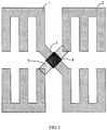
FIG. 1 is a structural schematic diagram of forming a touch electrode and a first conductive bridge in a fabrication method of a grating substrate provided by an embodiment of the invention; -
FIG. 2 is a schematic diagram of forming an insulating spacing layer on the basis ofFIG. 1 ; and -
FIG. 3 is a structural schematic diagram of a grating substrate after a second conductive bridge is formed. - In order to make objects, technical details and advantages of the embodiments of the invention apparent, the technical solutions of the embodiment will be described in a clearly and fully understandable way in connection with the drawings related to the embodiments of the invention. It is obvious that the described embodiments are just a part but not all of the embodiments of the invention. Based on the described embodiments herein, those skilled in the art can obtain other embodiment(s), without any inventive work, which should be within the scope of the invention.
- Hereinafter, embodiments of the present invention will be further illustrated in detail in conjunction with the accompanying drawings. The following embodiments are not to limit the scope of the embodiments of the invention.
- A fabrication method of a grating substrate provided by the present embodiment comprises steps of:
- Step 1: forming an array of comb-shaped, opaque touch electrodes and a first conductive bridge on a base substrate, wherein the array of touch electrodes includes a plurality of first touch electrodes and a plurality of second touch electrodes which are disconnected from each other, and each of the plurality of first touch electrodes and the plurality of second touch electrodes is comb-shaped and opaque; and the first touch electrodes in the array are connected via the first conductive bridge.
- Step 2: forming an insulating spacing layer on the base substrate on which the array of the touch electrodes and the plurality of first conductive bridges are formed, to cover the first conductive bridge.
- Step 3: forming a second conductive bridge on the insulating spacing layer, the second conductive bridge connecting the second touch electrodes to each other in the array.
- Therein, the opaque touch electrode may be a metal electrode.
- In the embodiment of the present invention, the touch electrode is made to be an opaque comb-shaped electrode, so that the touch electrode can be used as not only a touch electrode of a touch screen but also an electrode of a 3D slit grating, so as to achieve both a touch function and a 3D light-splitting function at the same time.
- Exemplarily, an exemplary description of the fabrication method of the grating substrate is given with reference to
FIGs. 1-3 ; for simplicity, only four touch electrodes are shown inFIGs. 1-3 , and more touch electrodes are not shown. - In
step 1, as shown inFIG. 1 , in order to save the fabrication process, a first conductive bridge 3 is made of the same material with the touch electrode, so while an array of comb-shaped, opaque touch electrodes (including a plurality offirst touch electrodes 1 and a plurality of second touch electrodes 2) is formed on the base substrate, the first conductive bridge 3 is formed too, and the first conductive bridge 3 is used to connect a plurality offirst touch electrodes 1. The first conductive bridge 3 and the touch electrodes may be fabricated by using a patterning process (the patterning process generally includes coating a photoresist, exposing, developing, etching, removing the photoresist and so on). - As shown in
FIG. 2 , aninsulating spacing layer 4 covering the first conductive bridge 3 may cover the entire base substrate (when it covers the entire base substrate, through holes are formed in regions of the insulating spacing layer corresponding to regions where the second touch electrode and the second conductive bridge are connected), or may only cover a region where the first conductive bridge is formed, or may only cover an overlapping region between the second conductive bridge to be formed and the first conductive bridge. The final grating substrate is shown inFIG. 3 , and in the embodiment, theinsulating spacing layer 4 is shown to only cover the overlapping region between the second conductive bridge to be formed and the first conductive bridge, to save material. - Exemplarily, when the insulating
spacing layer 4 is formed, a layer of photoresist may be formed at first, and the photoresist in the region where the insulatingspacing layer 4 is to be formed is removed, then a layer of insulating spacing material is formed, and finally the photoresist is removed, so that the insulating spacing material covered the photoresist is removed altogether, to finally form the insulatingspacing layer 4. - In step 3, when a second conductive bridge is formed, a layer of photoresist may be formed at first, and the photoresist in the region where the second conductive bridge is to be formed is removed, then a layer of conductive material (e.g., metal) is formed, and finally the photoresist is removed, so that the conductive material covered the photoresist is removed altogether, to finally form a second
conductive bridge 5 to connect with thesecond touch electrode 2. - Further, after the second
conductive bridge 5 is formed, a protective layer may be formed to protect the grating substrate. - Further, the base substrate may be a color filter (CF) substrate, and a plurality of touch electrodes and the first and second conductive bridges may be formed on a side of the base substrate opposite to a color filter, so that no additional grating alignment is needed when the slit grating is attached to the display panel, thus avoiding the alignment deviation. Of course, for One Glass Solution (OGS), they may also be formed inside the protective layer (Cover).
- In order not to affect the display effect, further, in each comb-shaped touch electrode, a connection bar for connecting comb teeth (as shown in the dashed line box in
FIG. 3 ) corresponds to a black matrix of the base substrate. - A fabrication method of a grating substrate provided by the present embodiment comprises steps of:
- Step 1: forming a second conductive bridge at a predetermined position on a base substrate.
- Step 2: forming an insulating spacing layer on the base substrate on which the second conductive bridge is formed, to make the insulating spacing layer cover the second conductive bridge.
- Step 3: forming an array of comb-shaped, opaque touch electrodes and a first conductive bridge on the base substrate on which the second conductive bridge and the insulating spacing layer are formed, wherein the array of touch electrodes includes a plurality of first touch electrodes and a plurality of second touch electrodes which are disconnected from each other, and each of the plurality of first touch electrodes and the plurality of second touch electrodes is comb-shaped and opaque, and the plurality of first touch electrodes in the array are connected together via the first conductive bridge, while the plurality of second touch electrodes are connected together via the second conductive bridge, and the insulating spacing layer is arranged between the first conductive bridge and the second conductive bridge.
- Exemplarily, when the second conductive bridge is formed, a layer of photoresist may be formed at first, and the photoresist in the region where the second conductive bridge is to be formed is removed, then a layer of conductive material (e.g., metal) is formed, and finally the photoresist is removed, so that the conductive material covered the photoresist is removed altogether, to finally form the second conductive bridge; or a layer of conductive material is formed at first, and then fabrication is performed by a patterning process (the patterning process generally includes coating photoresist, exposing, developing, etching, removing the photoresist and so on).
- Exemplarily, the insulating spacing layer covering the second conductive bridge may cover the entire base substrate (when it covers the entire base substrate, through holes are formed in the insulating spacing layer corresponding to regions where the second touch electrode and the second conductive bridge are connected), or may only cover a region where the second conductive bridge is formed, or may only cover an overlapping region between the first conductive bridge to be formed and the second conductive bridge.
- Exemplarily, when the array of touch electrodes and the first conductive bridge are formed, in order to save the fabrication process, the first conductive bridge is made of the same material with the touch electrode, so while an array of comb-shaped, opaque touch electrodes (including the first touch electrodes and the second touch electrodes) is formed on the base substrate, the first conductive bridge is formed too, to connect the first touch electrodes. The first conductive bridge 3 and the touch electrodes may be fabricated by a patterning process (the patterning process generally includes coating a photoresist, exposing, developing, etching, removing the photoresist and so on). Meanwhile the second conductive bridge formed in
step 1 is used to connect the second touch electrodes of the array together, and the first conductive bridge and the second conductive bridge is spaced by the insulating spacing layer. - Further, after the first conductive bridge is formed, a protection layer may be formed to protect the grating substrate.
- Further, the base substrate may be a color filter (CF) substrate, and a plurality of touch electrodes and the first and second conductive bridges may be formed on a side of the base substrate opposite to a color filter, so that no additional grating alignment is needed when the slit grating is attached to the display panel, thus avoiding an alignment deviation. Of course, for One Glass Solution (OGS), they may also be formed inside the protective layer (Cover).
- In order not to affect the display effect, further, in each comb-shaped touch electrode, a connection bar for connecting comb teeth is located in a region corresponding to a black matrix of the base substrate.
- As shown in
FIG. 3 , the embodiment of the invention further provides a grating substrate, comprising: a plurality of first conductive bridges, a plurality of comb-shaped, opaque first touch electrodes, and a plurality of comb-shaped, opaque second touch electrodes, formed in a same layer of a base substrate; a plurality of second conductive bridges, configured to connect the plurality of second touch electrodes, wherein the plurality of first touch electrodes are not connected to the plurality of second touch electrodes, and the plurality of first conductive bridges are configured to connect the plurality of first touch electrodes, and an insulating spacing layer is arranged between the first conductive bridges and the second conductive bridges. Each of the first touch electrodes and the second touch electrodes is a comb-shaped electrode. - Exemplarily, the base substrate is a color filter (CF) substrate, or for One Glass Solution (OGS), it may also be formed inside a protection layer (Cover).
- Exemplarily, as shown in the dashed line box in
FIG. 3 , in each comb-shaped electrode, a connection bar for connecting comb teeth is located in a region corresponding to a black matrix of the base substrate. - Exemplarily, the insulating spacing layer is only formed in overlapping regions of the first conductive bridges and the second conductive bridges. Or, the insulating spacing layer covers the entire base substrate, in which a plurality of through holes are formed to connect the plurality of second touch electrodes and the second conductive bridges.
- Exemplarily, the plurality of first conductive bridges, the plurality of comb-shaped, opaque first touch electrodes, and the plurality of comb-shaped, opaque second touch electrodes are made from same material.
- In the grating substrate provided by the embodiment of the present invention, the touch electrode is an opaque comb-shaped electrode, which can be used as not only a touch electrode of a touch screen but also an electrode of a 3D slit grating, to achieve both a touch function and a 3D light-splitting function at the same time.
- An embodiment of the present invention further provides a display device, comprising a display panel and the grating substrate mentioned above disposed on a light outgoing side of the display panel.
- Exemplarily, the display panel may be a liquid crystal display panel, including: an array substrate; a color filter substrate, disposed opposite to the array substrate; and a liquid crystal layer, disposed between the array substrate and the color filter substrate, wherein the base substrate of the grating substrate is the color filter substrate, wherein the plurality of touch electrodes and the first and second conductive bridges may be formed on a side of base substrate opposite to a color filter.
- Exemplarily, the display panel may be an organic light-emitting display panel, including: an array substrate; an opposed substrate, disposed opposite to the array substrate, wherein the base substrate of the grating substrate is the opposed substrate, wherein the plurality of touch electrodes and the first and second conductive bridges may be formed on a side of the opposed substrate opposite to the array substrate.
- Exemplarily, the display device may be: a liquid crystal panel with a 3D display function, an OLED panel, a mobile phone, a tablet computer, a television, a display, a notebook computer, a digital photo frame, a navigator, or any other product or component having a display function.
- The embodiment of the invention being thus described, it will be obvious that the same may be varied in many ways. Such variations are not to be regarded as a departure from the spirit and scope of the invention, and all such modifications as would be obvious to those skilled in the art are intended to be included within the scope of the following claims.
- The present application claims priority of Chinese Patent Application No.
201410253654.5 filed on June 9, 2014
Claims (21)
- A fabrication method of a grating substrate, comprising:forming an array of comb-shaped, opaque touch electrodes and a plurality of first conductive bridges on a base substrate, wherein the array of touch electrodes comprises a plurality of first touch electrodes and a plurality of second touch electrodes which are disconnected from each other, and the plurality of first touch electrodes in the array are connected to each other by the first conductive bridges;forming an insulating spacing layer on the base substrate on which the array of the touch electrodes and the plurality of first conductive bridges are formed, the insulating spacing layer covering the first conductive bridges; andforming second conductive bridges on the insulating spacing layer, the plurality of second touch electrodes in the array being connected to each other by the second conductive bridges.
- The fabrication method of the grating substrate according to claim 1, wherein the forming an array of comb-shaped, opaque touch electrodes and a plurality of first conductive bridges on a base substrate comprises:forming the array of comb-shaped, opaque touch electrodes on the base substrate, meanwhile forming the first conductive bridges, to connect the plurality of first touch electrodes in the array.
- The fabrication method of the grating substrate according to claim 1, wherein the forming an insulating spacing layer on the base substrate on which the array of the touch electrodes and the plurality of first conductive bridges are formed comprises:forming the insulating spacing layer in overlapping regions between the second conductive bridges and the first conductive bridges.
- The fabrication method of the grating substrate according to claim 1, wherein the base substrate is a color filter substrate, and in each of the comb-shaped touch electrodes, a connection bar for connecting comb teeth corresponds to a black matrix of the base substrate.
- The fabrication method of the grating substrate according to any one of claims 1 to 4, after forming the second conductive bridges, further comprising: forming a protective layer.
- The fabrication method of the grating substrate according to claim 1, wherein the forming an insulating spacing layer on the base substrate on which the array of the touch electrodes and the plurality of first conductive bridges are formed comprises: forming the insulating spacing layer on the entire base substrate on which the array of the touch electrodes and the plurality of first conductive bridges are formed.
- The fabrication method of the grating substrate according to claim 3, wherein the forming the insulating spacing layer in overlapping regions between the second conductive bridges and the first conductive bridges comprises:coating a photoresist on the base substrate on which the array of the touch electrodes and the plurality of first conductive bridges are formed;removing the photoresist from the overlapping regions between the second conductive bridges and the first conductive bridges;then forming a layer of insulating spacing material;removing the photoresist, to form the insulating spacing layer.
- The fabrication method of the grating substrate according to claim 1, wherein the forming second conductive bridges on the insulating spacing layer comprises:forming a layer of photoresist on the insulating spacing layer;removing the photoresist from regions in which the second conductive bridges are to be formed;then forming a layer of conductive material;removing the photoresist, to form the second conductive bridges.
- A fabrication method of a grating substrate, comprising:forming second conductive bridges at predetermined positions on a base substrate;forming an insulating spacing layer on the base substrate on which the second conductive bridges are formed, to make the insulating spacing layer cover the second conductive bridges;forming an array of comb-shaped, opaque touch electrodes and a plurality of first conductive bridges on the base substrate on which the second conductive bridges and the insulating spacing layer are formed, wherein the array of touch electrodes comprises a plurality of first touch electrodes and a plurality of second touch electrodes which are disconnected from each other, and the plurality of first touch electrodes in the array are connected to each other by the first conductive bridges, while the plurality of second touch electrodes in the array are connected to each other by the second conductive bridges, and the insulating spacing layer is arranged between the first conductive bridges and the second conductive bridges.
- The fabrication method of the grating substrate according to claim 9, wherein the forming an insulating spacing layer on the base substrate on which the second conductive bridges are formed, to make the insulating spacing layer cover the second conductive bridges comprises:forming the insulating spacing layer in overlapping regions between the second conductive bridges and the first conductive bridges.
- The fabrication method of the grating substrate according to claim 9, wherein the forming an array of comb-shaped, opaque touch electrodes and a plurality of first conductive bridges on the base substrate on which the second conductive bridges and the insulating spacing layer are formed comprises:forming the array of comb-shaped, opaque touch electrodes on the base substrate, meanwhile forming the plurality of first conductive bridges, to connect the plurality of first touch electrodes.
- The fabrication method of the grating substrate according to claim 9, wherein the base substrate is a color filter substrate, and in each of the comb-shaped touch electrodes, a connection bar for connecting comb teeth corresponds to a black matrix of the base substrate.
- The fabrication method of the grating substrate according to claim 9, after forming an array of comb-shaped, opaque touch electrodes and the first conductive bridges, further comprising: forming a protective layer.
- The fabrication method of the grating substrate according to claim 9, wherein the forming an insulating spacing layer on the base substrate on which the second conductive bridges are formed comprises:forming the insulating spacing layer on the entire base substrate on which the second conductive bridges are formed.
- The fabrication method of the grating substrate according to claim 10, wherein the forming the insulating spacing layer in overlapping regions between the second conductive bridges and the first conductive bridges comprises:coating a photoresist on the base substrate on which the second conductive bridges are formed;removing the photoresist from the overlapping regions between the second conductive bridges and the first conductive bridges;then forming a layer of insulating spacing material; andremoving the photoresist, to form the insulating spacing layer.
- A grating substrate, comprising:a plurality of first conductive bridges, a plurality of comb-shaped, opaque first touch electrodes, and a plurality of comb-shaped, opaque second touch electrodes , formed in a same layer on a base substrate;a plurality of second conductive bridges, configured to connect the plurality of second touch electrodes,wherein the plurality of first touch electrodes are not connected to the plurality of second touch electrodes, the plurality of first conductive bridges are configured to connect the plurality of first touch electrodes, and an insulating spacing layer is arranged between the first conductive bridges and the second conductive bridges.
- The grating substrate according to claim 16, wherein the base substrate is a color filter substrate, and in each of the comb-shaped touch electrodes, a connection bar for connecting comb teeth corresponds to a black matrix of the base substrate.
- The grating substrate according to claim 16, wherein the insulating spacing layer is only formed in overlapping regions of the first conductive bridges and the second conductive bridges.
- The grating substrate according to claim 16, wherein the insulating spacing layer covers the entire base substrate, in which a plurality of through holes are formed to connect the plurality of second touch electrodes and the second conductive bridges.
- The grating substrate according to claim 16, wherein the plurality of first conductive bridges, the plurality of comb-shaped, opaque first touch electrodes, and the plurality of comb-shaped, opaque second touch electrodes are made from a same material.
- A display device, comprising the grating substrate according to any one of claims 16 to 20.
Applications Claiming Priority (2)
| Application Number | Priority Date | Filing Date | Title |
|---|---|---|---|
| CN201410253654.5A CN104123036B (en) | 2014-06-09 | 2014-06-09 | Grating substrate, manufacturing method thereof and display device |
| PCT/CN2014/088359 WO2015188539A1 (en) | 2014-06-09 | 2014-10-11 | Grating base plate and manufacturing method therefor, and display device |
Publications (3)
| Publication Number | Publication Date |
|---|---|
| EP3153919A1 true EP3153919A1 (en) | 2017-04-12 |
| EP3153919A4 EP3153919A4 (en) | 2018-01-03 |
| EP3153919B1 EP3153919B1 (en) | 2019-12-04 |
Family
ID=51768468
Family Applications (1)
| Application Number | Title | Priority Date | Filing Date |
|---|---|---|---|
| EP14861122.1A Active EP3153919B1 (en) | 2014-06-09 | 2014-10-11 | Grating base plate and manufacturing method therefor, and display device |
Country Status (4)
| Country | Link |
|---|---|
| US (1) | US9626026B2 (en) |
| EP (1) | EP3153919B1 (en) |
| CN (1) | CN104123036B (en) |
| WO (1) | WO2015188539A1 (en) |
Families Citing this family (5)
| Publication number | Priority date | Publication date | Assignee | Title |
|---|---|---|---|---|
| CN107884854A (en) * | 2016-09-30 | 2018-04-06 | 京东方科技集团股份有限公司 | The preparation method of optical grating construction, display device and the optical grating construction |
| CN107957799B (en) * | 2016-10-14 | 2021-08-10 | 群创光电股份有限公司 | Touch control display panel |
| KR102161709B1 (en) * | 2017-05-08 | 2020-10-06 | 엘지디스플레이 주식회사 | Display device |
| CN106950630B (en) * | 2017-05-22 | 2019-10-01 | 京东方科技集团股份有限公司 | A kind of grating and 3 d display device |
| CN107515475B (en) * | 2017-10-11 | 2020-05-01 | 上海天马微电子有限公司 | Stereoscopic display device and manufacturing method thereof |
Family Cites Families (18)
| Publication number | Priority date | Publication date | Assignee | Title |
|---|---|---|---|---|
| JP4407872B2 (en) * | 2001-07-16 | 2010-02-03 | 富士通株式会社 | Touch panel device |
| TW200901014A (en) * | 2007-06-28 | 2009-01-01 | Sense Pad Tech Co Ltd | Touch panel device |
| US10282040B2 (en) * | 2009-03-20 | 2019-05-07 | Tpk Touch Solutions (Xiamen) Inc. | Capacitive touch circuit pattern and manufacturing method thereof |
| US8884922B2 (en) * | 2010-04-01 | 2014-11-11 | Sharp Kabushiki Kaisha | Display device including touch panel and parallax barrier sharing single board |
| WO2013018591A1 (en) * | 2011-07-29 | 2013-02-07 | シャープ株式会社 | Touch panel substrate and electro-optic device |
| KR101363151B1 (en) * | 2011-09-06 | 2014-02-14 | 삼성전자주식회사 | Transparent circuit substrate for touchscreen, method for fabricating the same and touchscreen comprising the same |
| CN103293778B (en) * | 2012-03-31 | 2015-09-02 | 上海天马微电子有限公司 | Touch liquid crystal grating device and 3D/2D flat panel display device |
| US9116358B2 (en) * | 2012-05-17 | 2015-08-25 | Innocom Technology(Shenzhen) Co., Ltd. | 2D/3D switchable parallax barrier display |
| TWI486668B (en) | 2012-05-24 | 2015-06-01 | Chunghwa Picture Tubes Ltd | Panel structure |
| CN102830555B (en) | 2012-08-31 | 2015-01-07 | 北京京东方光电科技有限公司 | Touch liquid crystal grating and 3D touch display device |
| CN103049156B (en) * | 2012-12-13 | 2015-12-23 | 北京京东方光电科技有限公司 | A kind of capacitance type in-cell touch panel and display device |
| CN103116233B (en) | 2013-01-23 | 2016-01-06 | 北京京东方光电科技有限公司 | A kind of touch LCD optical grating construction and 3D touch display unit |
| CN103149749B (en) * | 2013-02-06 | 2016-05-25 | 敦泰电子有限公司 | A kind of electrode structure and liquid crystal indicator |
| CN103309094B (en) * | 2013-03-29 | 2016-01-06 | 北京京东方光电科技有限公司 | The driving method of a kind of liquid crystal grating, 3D touch control display apparatus and liquid crystal grating |
| CN203133450U (en) | 2013-03-29 | 2013-08-14 | 北京京东方光电科技有限公司 | Liquid crystal grating and 3D (three-dimensional) touch display device |
| CN103558942B (en) * | 2013-11-08 | 2016-03-09 | 京东方科技集团股份有限公司 | Touch-screen and manufacture method thereof |
| CN103698926B (en) | 2013-12-31 | 2016-04-27 | 京东方科技集团股份有限公司 | A kind of display device and preparation method thereof |
| CN103941912B (en) * | 2014-03-25 | 2017-12-08 | 京东方科技集团股份有限公司 | A kind of touch-screen and preparation method thereof, 3D display device |
-
2014
- 2014-06-09 CN CN201410253654.5A patent/CN104123036B/en not_active Expired - Fee Related
- 2014-10-11 US US14/443,508 patent/US9626026B2/en not_active Expired - Fee Related
- 2014-10-11 EP EP14861122.1A patent/EP3153919B1/en active Active
- 2014-10-11 WO PCT/CN2014/088359 patent/WO2015188539A1/en not_active Ceased
Also Published As
| Publication number | Publication date |
|---|---|
| EP3153919A4 (en) | 2018-01-03 |
| EP3153919B1 (en) | 2019-12-04 |
| CN104123036A (en) | 2014-10-29 |
| WO2015188539A1 (en) | 2015-12-17 |
| US9626026B2 (en) | 2017-04-18 |
| US20160291742A1 (en) | 2016-10-06 |
| CN104123036B (en) | 2017-02-01 |
Similar Documents
| Publication | Publication Date | Title |
|---|---|---|
| EP2813886B1 (en) | 3d display device and manufacturing method therefor | |
| CN205862051U (en) | A kind of color membrane substrates and display device | |
| CN103558724B (en) | Liquid crystal prism, manufacturing method thereof and display device | |
| US9405144B2 (en) | Liquid crystal grating, 3D touch display device and driving method of liquid crystal grating | |
| US9626026B2 (en) | Grating substrate and fabrication method thereof, display device | |
| US9389719B2 (en) | Touch screen, method for manufacturing the same, 3D display apparatus | |
| US20150109666A1 (en) | Array substrate and manufacturing method thereof, 3d display device | |
| EP3217213A1 (en) | Array substrate, liquid crystal display panel and display device | |
| EP3199988B1 (en) | Color filter and manufacturing method thereof, display panel, display device and drive method thereof | |
| US11507234B2 (en) | Touch substrate, manufacturing method thereof, and display device | |
| US10216339B2 (en) | Display substrate and manufacturing method thereof, and display device | |
| US10215994B2 (en) | Display panel, method of manufacturing display panel, and display apparatus | |
| WO2016004725A1 (en) | Touch-type three-dimensional grating and display device | |
| JP2013182187A (en) | Display device and liquid crystal barrier element | |
| CN104849886B (en) | Display device and its driving method, production method | |
| CN104698663A (en) | Display device and driving method thereof | |
| US9886148B2 (en) | Touch screen, method for producing touch screen, touch display device | |
| US20160291335A1 (en) | Liquid crystal lens light splitting device and manufacturing method thereof, and stereoscopic display device | |
| US20150185910A1 (en) | Display device and method for preparing the same | |
| US10001853B2 (en) | Touch grating cell and touch stereoscopic display device | |
| US10497722B2 (en) | Array substrate and manufacturing method thereof, and liquid crystal display device | |
| US10795217B2 (en) | Liquid crystal grating and fabrication method thereof, and naked eye 3D display device | |
| US20180292664A1 (en) | Liquid crystal lens, method for producing the same, and display apparatus | |
| CN105807522A (en) | Array substrate, production method thereof and display panel | |
| KR20140085994A (en) | Display Device With Integrated Touch Screen and Method for Manufacturing The Same |
Legal Events
| Date | Code | Title | Description |
|---|---|---|---|
| PUAI | Public reference made under article 153(3) epc to a published international application that has entered the european phase |
Free format text: ORIGINAL CODE: 0009012 |
|
| STAA | Information on the status of an ep patent application or granted ep patent |
Free format text: STATUS: REQUEST FOR EXAMINATION WAS MADE |
|
| 17P | Request for examination filed |
Effective date: 20150518 |
|
| AK | Designated contracting states |
Kind code of ref document: A1 Designated state(s): AL AT BE BG CH CY CZ DE DK EE ES FI FR GB GR HR HU IE IS IT LI LT LU LV MC MK MT NL NO PL PT RO RS SE SI SK SM TR |
|
| AX | Request for extension of the european patent |
Extension state: BA ME |
|
| DAX | Request for extension of the european patent (deleted) | ||
| A4 | Supplementary search report drawn up and despatched |
Effective date: 20171201 |
|
| RIC1 | Information provided on ipc code assigned before grant |
Ipc: G06F 3/041 20060101ALI20171128BHEP Ipc: G02F 1/1343 20060101ALI20171128BHEP Ipc: G02B 27/26 20060101ALI20171128BHEP Ipc: H04N 13/04 00000000ALI20171128BHEP Ipc: G06F 3/044 20060101AFI20171128BHEP |
|
| STAA | Information on the status of an ep patent application or granted ep patent |
Free format text: STATUS: EXAMINATION IS IN PROGRESS |
|
| 17Q | First examination report despatched |
Effective date: 20181112 |
|
| RIC1 | Information provided on ipc code assigned before grant |
Ipc: G06F 3/041 20060101ALI20171128BHEP Ipc: G02F 1/1343 20060101ALI20171128BHEP Ipc: G02B 27/26 20060101ALI20171128BHEP Ipc: H04N 13/04 20060101ALI20171128BHEP Ipc: G06F 3/044 20060101AFI20171128BHEP |
|
| REG | Reference to a national code |
Ref country code: DE Ref legal event code: R079 Ref document number: 602014058038 Country of ref document: DE Free format text: PREVIOUS MAIN CLASS: G02F0001134300 Ipc: G06F0003044000 |
|
| GRAP | Despatch of communication of intention to grant a patent |
Free format text: ORIGINAL CODE: EPIDOSNIGR1 |
|
| STAA | Information on the status of an ep patent application or granted ep patent |
Free format text: STATUS: GRANT OF PATENT IS INTENDED |
|
| RIC1 | Information provided on ipc code assigned before grant |
Ipc: G06F 3/041 20060101ALI20190510BHEP Ipc: H04N 13/31 20180101ALI20190510BHEP Ipc: G02B 27/22 20180101ALI20190510BHEP Ipc: G06F 3/044 20060101AFI20190510BHEP |
|
| INTG | Intention to grant announced |
Effective date: 20190529 |
|
| GRAS | Grant fee paid |
Free format text: ORIGINAL CODE: EPIDOSNIGR3 |
|
| GRAA | (expected) grant |
Free format text: ORIGINAL CODE: 0009210 |
|
| STAA | Information on the status of an ep patent application or granted ep patent |
Free format text: STATUS: THE PATENT HAS BEEN GRANTED |
|
| AK | Designated contracting states |
Kind code of ref document: B1 Designated state(s): AL AT BE BG CH CY CZ DE DK EE ES FI FR GB GR HR HU IE IS IT LI LT LU LV MC MK MT NL NO PL PT RO RS SE SI SK SM TR |
|
| REG | Reference to a national code |
Ref country code: GB Ref legal event code: FG4D |
|
| REG | Reference to a national code |
Ref country code: CH Ref legal event code: EP |
|
| REG | Reference to a national code |
Ref country code: AT Ref legal event code: REF Ref document number: 1210210 Country of ref document: AT Kind code of ref document: T Effective date: 20191215 |
|
| REG | Reference to a national code |
Ref country code: IE Ref legal event code: FG4D |
|
| REG | Reference to a national code |
Ref country code: DE Ref legal event code: R096 Ref document number: 602014058038 Country of ref document: DE |
|
| REG | Reference to a national code |
Ref country code: NL Ref legal event code: MP Effective date: 20191204 |
|
| REG | Reference to a national code |
Ref country code: LT Ref legal event code: MG4D |
|
| PG25 | Lapsed in a contracting state [announced via postgrant information from national office to epo] |
Ref country code: SE Free format text: LAPSE BECAUSE OF FAILURE TO SUBMIT A TRANSLATION OF THE DESCRIPTION OR TO PAY THE FEE WITHIN THE PRESCRIBED TIME-LIMIT Effective date: 20191204 Ref country code: LV Free format text: LAPSE BECAUSE OF FAILURE TO SUBMIT A TRANSLATION OF THE DESCRIPTION OR TO PAY THE FEE WITHIN THE PRESCRIBED TIME-LIMIT Effective date: 20191204 Ref country code: GR Free format text: LAPSE BECAUSE OF FAILURE TO SUBMIT A TRANSLATION OF THE DESCRIPTION OR TO PAY THE FEE WITHIN THE PRESCRIBED TIME-LIMIT Effective date: 20200305 Ref country code: NO Free format text: LAPSE BECAUSE OF FAILURE TO SUBMIT A TRANSLATION OF THE DESCRIPTION OR TO PAY THE FEE WITHIN THE PRESCRIBED TIME-LIMIT Effective date: 20200304 Ref country code: LT Free format text: LAPSE BECAUSE OF FAILURE TO SUBMIT A TRANSLATION OF THE DESCRIPTION OR TO PAY THE FEE WITHIN THE PRESCRIBED TIME-LIMIT Effective date: 20191204 Ref country code: BG Free format text: LAPSE BECAUSE OF FAILURE TO SUBMIT A TRANSLATION OF THE DESCRIPTION OR TO PAY THE FEE WITHIN THE PRESCRIBED TIME-LIMIT Effective date: 20200304 Ref country code: FI Free format text: LAPSE BECAUSE OF FAILURE TO SUBMIT A TRANSLATION OF THE DESCRIPTION OR TO PAY THE FEE WITHIN THE PRESCRIBED TIME-LIMIT Effective date: 20191204 |
|
| PG25 | Lapsed in a contracting state [announced via postgrant information from national office to epo] |
Ref country code: RS Free format text: LAPSE BECAUSE OF FAILURE TO SUBMIT A TRANSLATION OF THE DESCRIPTION OR TO PAY THE FEE WITHIN THE PRESCRIBED TIME-LIMIT Effective date: 20191204 Ref country code: HR Free format text: LAPSE BECAUSE OF FAILURE TO SUBMIT A TRANSLATION OF THE DESCRIPTION OR TO PAY THE FEE WITHIN THE PRESCRIBED TIME-LIMIT Effective date: 20191204 |
|
| PG25 | Lapsed in a contracting state [announced via postgrant information from national office to epo] |
Ref country code: AL Free format text: LAPSE BECAUSE OF FAILURE TO SUBMIT A TRANSLATION OF THE DESCRIPTION OR TO PAY THE FEE WITHIN THE PRESCRIBED TIME-LIMIT Effective date: 20191204 |
|
| PG25 | Lapsed in a contracting state [announced via postgrant information from national office to epo] |
Ref country code: PT Free format text: LAPSE BECAUSE OF FAILURE TO SUBMIT A TRANSLATION OF THE DESCRIPTION OR TO PAY THE FEE WITHIN THE PRESCRIBED TIME-LIMIT Effective date: 20200429 Ref country code: EE Free format text: LAPSE BECAUSE OF FAILURE TO SUBMIT A TRANSLATION OF THE DESCRIPTION OR TO PAY THE FEE WITHIN THE PRESCRIBED TIME-LIMIT Effective date: 20191204 Ref country code: ES Free format text: LAPSE BECAUSE OF FAILURE TO SUBMIT A TRANSLATION OF THE DESCRIPTION OR TO PAY THE FEE WITHIN THE PRESCRIBED TIME-LIMIT Effective date: 20191204 Ref country code: RO Free format text: LAPSE BECAUSE OF FAILURE TO SUBMIT A TRANSLATION OF THE DESCRIPTION OR TO PAY THE FEE WITHIN THE PRESCRIBED TIME-LIMIT Effective date: 20191204 Ref country code: NL Free format text: LAPSE BECAUSE OF FAILURE TO SUBMIT A TRANSLATION OF THE DESCRIPTION OR TO PAY THE FEE WITHIN THE PRESCRIBED TIME-LIMIT Effective date: 20191204 Ref country code: CZ Free format text: LAPSE BECAUSE OF FAILURE TO SUBMIT A TRANSLATION OF THE DESCRIPTION OR TO PAY THE FEE WITHIN THE PRESCRIBED TIME-LIMIT Effective date: 20191204 |
|
| PG25 | Lapsed in a contracting state [announced via postgrant information from national office to epo] |
Ref country code: IS Free format text: LAPSE BECAUSE OF FAILURE TO SUBMIT A TRANSLATION OF THE DESCRIPTION OR TO PAY THE FEE WITHIN THE PRESCRIBED TIME-LIMIT Effective date: 20200404 Ref country code: SK Free format text: LAPSE BECAUSE OF FAILURE TO SUBMIT A TRANSLATION OF THE DESCRIPTION OR TO PAY THE FEE WITHIN THE PRESCRIBED TIME-LIMIT Effective date: 20191204 Ref country code: SM Free format text: LAPSE BECAUSE OF FAILURE TO SUBMIT A TRANSLATION OF THE DESCRIPTION OR TO PAY THE FEE WITHIN THE PRESCRIBED TIME-LIMIT Effective date: 20191204 |
|
| REG | Reference to a national code |
Ref country code: DE Ref legal event code: R097 Ref document number: 602014058038 Country of ref document: DE |
|
| REG | Reference to a national code |
Ref country code: AT Ref legal event code: MK05 Ref document number: 1210210 Country of ref document: AT Kind code of ref document: T Effective date: 20191204 |
|
| PLBE | No opposition filed within time limit |
Free format text: ORIGINAL CODE: 0009261 |
|
| STAA | Information on the status of an ep patent application or granted ep patent |
Free format text: STATUS: NO OPPOSITION FILED WITHIN TIME LIMIT |
|
| PG25 | Lapsed in a contracting state [announced via postgrant information from national office to epo] |
Ref country code: DK Free format text: LAPSE BECAUSE OF FAILURE TO SUBMIT A TRANSLATION OF THE DESCRIPTION OR TO PAY THE FEE WITHIN THE PRESCRIBED TIME-LIMIT Effective date: 20191204 |
|
| 26N | No opposition filed |
Effective date: 20200907 |
|
| PG25 | Lapsed in a contracting state [announced via postgrant information from national office to epo] |
Ref country code: SI Free format text: LAPSE BECAUSE OF FAILURE TO SUBMIT A TRANSLATION OF THE DESCRIPTION OR TO PAY THE FEE WITHIN THE PRESCRIBED TIME-LIMIT Effective date: 20191204 Ref country code: PL Free format text: LAPSE BECAUSE OF FAILURE TO SUBMIT A TRANSLATION OF THE DESCRIPTION OR TO PAY THE FEE WITHIN THE PRESCRIBED TIME-LIMIT Effective date: 20191204 Ref country code: AT Free format text: LAPSE BECAUSE OF FAILURE TO SUBMIT A TRANSLATION OF THE DESCRIPTION OR TO PAY THE FEE WITHIN THE PRESCRIBED TIME-LIMIT Effective date: 20191204 |
|
| PG25 | Lapsed in a contracting state [announced via postgrant information from national office to epo] |
Ref country code: IT Free format text: LAPSE BECAUSE OF FAILURE TO SUBMIT A TRANSLATION OF THE DESCRIPTION OR TO PAY THE FEE WITHIN THE PRESCRIBED TIME-LIMIT Effective date: 20191204 |
|
| REG | Reference to a national code |
Ref country code: CH Ref legal event code: PL |
|
| GBPC | Gb: european patent ceased through non-payment of renewal fee |
Effective date: 20201011 |
|
| PG25 | Lapsed in a contracting state [announced via postgrant information from national office to epo] |
Ref country code: MC Free format text: LAPSE BECAUSE OF FAILURE TO SUBMIT A TRANSLATION OF THE DESCRIPTION OR TO PAY THE FEE WITHIN THE PRESCRIBED TIME-LIMIT Effective date: 20191204 Ref country code: LU Free format text: LAPSE BECAUSE OF NON-PAYMENT OF DUE FEES Effective date: 20201011 |
|
| REG | Reference to a national code |
Ref country code: BE Ref legal event code: MM Effective date: 20201031 |
|
| PG25 | Lapsed in a contracting state [announced via postgrant information from national office to epo] |
Ref country code: FR Free format text: LAPSE BECAUSE OF NON-PAYMENT OF DUE FEES Effective date: 20201031 |
|
| PG25 | Lapsed in a contracting state [announced via postgrant information from national office to epo] |
Ref country code: GB Free format text: LAPSE BECAUSE OF NON-PAYMENT OF DUE FEES Effective date: 20201011 Ref country code: LI Free format text: LAPSE BECAUSE OF NON-PAYMENT OF DUE FEES Effective date: 20201031 Ref country code: CH Free format text: LAPSE BECAUSE OF NON-PAYMENT OF DUE FEES Effective date: 20201031 Ref country code: BE Free format text: LAPSE BECAUSE OF NON-PAYMENT OF DUE FEES Effective date: 20201031 |
|
| PG25 | Lapsed in a contracting state [announced via postgrant information from national office to epo] |
Ref country code: IE Free format text: LAPSE BECAUSE OF NON-PAYMENT OF DUE FEES Effective date: 20201011 |
|
| PGFP | Annual fee paid to national office [announced via postgrant information from national office to epo] |
Ref country code: DE Payment date: 20211020 Year of fee payment: 8 |
|
| PG25 | Lapsed in a contracting state [announced via postgrant information from national office to epo] |
Ref country code: TR Free format text: LAPSE BECAUSE OF FAILURE TO SUBMIT A TRANSLATION OF THE DESCRIPTION OR TO PAY THE FEE WITHIN THE PRESCRIBED TIME-LIMIT Effective date: 20191204 Ref country code: MT Free format text: LAPSE BECAUSE OF FAILURE TO SUBMIT A TRANSLATION OF THE DESCRIPTION OR TO PAY THE FEE WITHIN THE PRESCRIBED TIME-LIMIT Effective date: 20191204 Ref country code: CY Free format text: LAPSE BECAUSE OF FAILURE TO SUBMIT A TRANSLATION OF THE DESCRIPTION OR TO PAY THE FEE WITHIN THE PRESCRIBED TIME-LIMIT Effective date: 20191204 |
|
| PG25 | Lapsed in a contracting state [announced via postgrant information from national office to epo] |
Ref country code: MK Free format text: LAPSE BECAUSE OF FAILURE TO SUBMIT A TRANSLATION OF THE DESCRIPTION OR TO PAY THE FEE WITHIN THE PRESCRIBED TIME-LIMIT Effective date: 20191204 |
|
| REG | Reference to a national code |
Ref country code: DE Ref legal event code: R119 Ref document number: 602014058038 Country of ref document: DE |
|
| PG25 | Lapsed in a contracting state [announced via postgrant information from national office to epo] |
Ref country code: DE Free format text: LAPSE BECAUSE OF NON-PAYMENT OF DUE FEES Effective date: 20230503 |