EP3152152B1 - Miniatur-halbtonbild aus einer anordung von kolloidnanopartikeln und verfahren zu dessen herstellung - Google Patents
Miniatur-halbtonbild aus einer anordung von kolloidnanopartikeln und verfahren zu dessen herstellung Download PDFInfo
- Publication number
- EP3152152B1 EP3152152B1 EP15732424.5A EP15732424A EP3152152B1 EP 3152152 B1 EP3152152 B1 EP 3152152B1 EP 15732424 A EP15732424 A EP 15732424A EP 3152152 B1 EP3152152 B1 EP 3152152B1
- Authority
- EP
- European Patent Office
- Prior art keywords
- injection
- nanoparticles
- miniature
- colloidal
- assembly
- Prior art date
- Legal status (The legal status is an assumption and is not a legal conclusion. Google has not performed a legal analysis and makes no representation as to the accuracy of the status listed.)
- Active
Links
Images




Classifications
-
- B—PERFORMING OPERATIONS; TRANSPORTING
- B81—MICROSTRUCTURAL TECHNOLOGY
- B81C—PROCESSES OR APPARATUS SPECIALLY ADAPTED FOR THE MANUFACTURE OR TREATMENT OF MICROSTRUCTURAL DEVICES OR SYSTEMS
- B81C1/00—Manufacture or treatment of devices or systems in or on a substrate
- B81C1/00349—Creating layers of material on a substrate
- B81C1/00373—Selective deposition, e.g. printing or microcontact printing
-
- B—PERFORMING OPERATIONS; TRANSPORTING
- B82—NANOTECHNOLOGY
- B82Y—SPECIFIC USES OR APPLICATIONS OF NANOSTRUCTURES; MEASUREMENT OR ANALYSIS OF NANOSTRUCTURES; MANUFACTURE OR TREATMENT OF NANOSTRUCTURES
- B82Y30/00—Nanotechnology for materials or surface science, e.g. nanocomposites
-
- G—PHYSICS
- G03—PHOTOGRAPHY; CINEMATOGRAPHY; ANALOGOUS TECHNIQUES USING WAVES OTHER THAN OPTICAL WAVES; ELECTROGRAPHY; HOLOGRAPHY
- G03G—ELECTROGRAPHY; ELECTROPHOTOGRAPHY; MAGNETOGRAPHY
- G03G15/00—Apparatus for electrographic processes using a charge pattern
- G03G15/22—Apparatus for electrographic processes using a charge pattern involving the combination of more than one step according to groups G03G13/02 - G03G13/20
- G03G15/221—Machines other than electrographic copiers, e.g. electrophotographic cameras, electrostatic typewriters
Definitions
- the present invention relates to micro- / nanometric patterns or miniature halftone images formed by a nanoparticle assembly and a method of making such patterns.
- Halftone images have the remarkable ability to translate value or Corposcuro contrasts by using a binary base, for example, white and black from fixed points called pixels of variable size, shape and relative arrangement.
- Such halftone patterns can be conventionally achieved by inkjet printers that use a plurality of small ink drops mixed, deposited, and absorbed on the same point of a substrate substrate by printing forces. capillarity.
- WO 2013/071960 A1 discloses a method of marking a coding pattern of digital information on a surface.
- the technical problem is to fabricate micro- / nanometric patterns or halftone images in which the number of half-tones (or tonality) is high in relation to the state of the art and the spatial resolution of the points. printing is minimal.
- micro / nanometric patterns of up to several tens of thousands of half-tones on a pixel of 1 ⁇ m 2 , and whose maximum spatial resolution of the printing points is of the order of a few nanometers.
- the invention also provides a miniature halftone pattern on an electret substrate corresponding to a halftone image formed by a two-dimensional arrangement of halftone pixels included in a set of halftone colors ranging from light to dark.
- a miniature halftone pattern on an electret substrate corresponding to a halftone image formed by a two-dimensional arrangement of halftone pixels included in a set of halftone colors ranging from light to dark.
- each injection point of the miniature pattern being defined by two-dimensional coordinates considered on the surface and a level of halftone included in a set of halftones ranging from light to dark, the bidimensional coordinates of the injection points respectively corresponding to the coordinates of the pixels of the image, and the half-tone levels of the injection points respectively corresponding to the halftone levels of the associated pixels, so as to reproduce the image on a reduced scale, on each injection point being fixed an elementary colloidal assembly of colloidal nanoparticles, neutral or quasi-neutral electrically and electrically polarizable by the action of an external electric field, trapped on the substrate through die
- the invention also relates to an anti-counterfeiting and traceability marking label comprising a miniature halftone pattern on an electret substrate defined above by the method defined above.
- the nanoparticles can furthermore have specific physical properties, for example photoluminescence properties, making it possible to provide an additional means of concealing information in the halftone image.
- a method 2 of manufacturing a miniature halftone pattern on an electret substrate generally comprises a set of successively executed steps.
- a halftone image file is generated electronically in the form of a computer file.
- the halftone image is formed by an array of halftone pixels having halftone characteristics ranging from light to dark. Each pixel is electronically defined at least by two-dimensional coordinates and an associated halftone coding value.
- a computer format of black and white image is chosen in the set of image formats formed by BMP, GIF, JPEG, LBM, PCX, PNG, PNM, TGA, TIFF , WEBBP, XCF, XPM, XV.
- the pixel image file is converted into an injection script, executable by control software of an electric charge injection device.
- the injection script is configured to reproduce the image on a reduced scale on a planar receiving surface of the electret substrate, provided to receive the miniature pattern and located at a predetermined location, by matching each pixel a charge injection point on the receiving surface, the charges may be electric charges or polarization charges.
- the injection point is characterized by a voltage and an injection time which depend on the half-tone level of the corresponding pixel according to a monotonic variation function of halftone level conversion into injection voltage, so that the map of the surface potential that will be obtained after injection of the charges on the receiving surface of the electret substrate at the injection points will reproduce the image on a reduced scale.
- an injection pitch defined as the center-to-center distance of two immediately adjacent injection points, is chosen so that the size of the desired miniature image is equal to the size of the image expressed in pixels minus one multiplied by the injection pitch.
- a third step 8 charges are injected onto and into the electret substrate at the surface area by a conventional injection method according to the injection script obtained in the second step 6.
- the conventional method of charge injection is for example that described in the French patent application entitled “Micro / nano structures of colloidal nanoparticles fixed on an electret substrate and method of manufacturing such micro / nano structures” filed March 8, 2013 and having the deposit number FR 52092 .
- a fourth step 10 the electret substrate having the receiving surface inscribed by the surface potential according to the desired pattern of electrical charges, is contacted with a colloidal dispersion for a sufficiently long contact time and less than or equal to fifteen minutes.
- the contacting times are between 30 seconds and a few minutes.
- the colloidal dispersion here comprises colloidal nanoparticles neutral or quasi-neutral electrically and electrically polarizable under the action of an external electric field, and a dispersion medium, in the form of a liquid solvent or a gas, substantially free of electric polarization action, wherein the colloidal nanoparticles are dispersed.
- colloidal nanoparticles are electrically charged.
- the electret material is a material comprised in the group formed by poly-methyl methacrylates (PMMA), cyclic olefin copolymers (CoC), polyethylene terephthalate (PET), polydimethylsiloxane (PDMS) polypropylenes (PP), polycarbonates (PC), polystyrenes (PS), polyvinyl chloride (PVC), polytetrafluoroethylenes (PFTE), triglycine sulfate (TGS), polyvinylidene fluoride (PVDF), silicon nitride (Si 3 N 4 ), silicon oxide (SiO 2 ), Si 3 N 4 / SiO 2 / Si compound (NOS).
- PMMA poly-methyl methacrylates
- CoC polyethylene terephthalate
- PDMS polydimethylsiloxane
- PP polypropylenes
- PC polycarbonates
- PS polystyrenes
- PVC polyvinyl chloride
- the substantially neutral and electrically polarizable colloidal nanoparticles or the electrically charged colloidal nanoparticles are stabilized compounds by themselves or by ligands and / or charges, having physical properties comprised in the set formed by the plasmonic properties.
- the basic colloidal nanoparticles have a solid core and, where appropriate, a shell, and are included in the group formed by the latex, SiO 2 , TiO 2 , ZrO 2 ; CdS, CdSe, PbSe, GaAs, GaN, InP, In 2 O 3 , ZnS, ZnO, MoS 2 , Si, C, ITO, Fe 2 O 3 , Fe 3 O 4 , Co, Fe-Co, Fe 3 C, Fe 5 C 2 , Ni; Au, Ag, Cu, Pt, and bi-metallic nanoparticles; WO 3 ; NaLnF 4 , lanthanide fluorides (LnF 3 ), lanthanide oxides (Ln 2 O 3 ), zirconates, silicates, hydroxides (Ln (OH) 3 ) and oxide sulfides doped or not with one or more lanthanides different (Ln denoting a lanthanide), the mixtures of these compounds.
- the solvent is comprised of all of pentane, iso-pentane, hexane, heptane, octane, nonane, decane. cyclopentane, cyclohexane, cycloheptane, cyclooctane, cyclohexene, benzene, toluene, methylcyclohexane, xylene, mesithylene, chloroform, methylene chloride, tetrachlorethylene.
- the dispersing medium is a non-polarizing dispersing gas
- the dispersing gas is comprised in the combination formed by the N 2 dinitrogen, argon Ar, and air.
- the small size of the halftone pattern obtained by the general method of Figure 1 makes the location of the complex pattern on large electret surfaces devoid of registration.
- a second non-visible image before decoding is encoded in a first image, visible directly without image processing.
- the colloidal nanoparticles have the property of converting radiation in a near-infrared spectrum (NIR) into radiation in a first visible spectrum.
- NIR near-infrared spectrum
- the nanoparticles are nanoparticles of NaYF 4 doped with lanthanides.
- Nanoparticles are 28 nm diameter polarized and unloaded nanoparticles, coated with oleic acid, doped with Erbium and Ytterbium, luminescent, dispersed in hexane at a first colloidal concentration C1 of 1.49 * 10 13 Nano Particles (NPs) / ml (which corresepond 0,12mg.ml -1).
- the assembly may not be compact.
- the final half-tent effect will be created by the variation of the projected surface density and the shape of the nanoparticle assembly on each of the sites corresponding to the injection points on the electret substrate, the density projected surface area being equal to the number of particles contained in the cylinder delimited by a surface unit.
- the notion of projected surface density merges with the notion of conventional surface density of nanoparticles.
- the final halftone effect can be a density variation effect without necessarily presence of compactness of the nanoparticles in the assembly.
- the voltages applied between the AFM tip and the electret substrate vary from +50 V, a value corresponding to a white pixel, to +75 V, a value corresponding to a black pixel.
- the surface potentials of the injection points vary correspondingly from a first lower surface potential V kfm1min +130 mV to a first higher surface potential V kfm1max + 950 mV.
- the injected electret substrate is immersed for 30 seconds in a bath of colloidal NaYF 4 nanoparticles of the first concentration C1 of 1.49 * 10 13 Nano Particles (NPs) / ml (that is to say 0.12 mg / ml). Then, after removal of the dispersion, the substrate is dried by evaporation of the solvent at room temperature. Under these conditions, the final assembly of the nanoparticles at an injection point when it takes place is compact, which can be multilayer or monolayer.
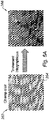
- the halftone pattern obtained is visible in a bright field as shown in FIG. Figure 2A which represents on the left a first raw view 52, that is to say without image processing, of the Mona Lisa 54 forming the pattern, and on the right a second view 56, improved in terms of noise filtering by an infographic processing .
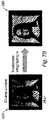
- the halftone pattern obtained is also visible in the dark field as illustrated in FIG. Figure 2B which on the left represents a first raw field view 62 of the same Mona Lisa 64, of better quality than the first raw field view 52, and to the right a second improved view 66 of the first raw view 62 in a dark field by a infographic processing.
- the same colloidal NaYF 4 nanoparticles are used in the same hexane dispersion at a second colloidal concentration C2, here identical to the first concentration C1 of the colloidal dispersion, ie equal to 1.49 * 10 13 Nano Particles (NPs) / ml (or 0.12 mg / ml).
- the second embodiment differs from the first embodiment by a second injection script in which the injection voltages applied between the AFM tip and the electret substrate vary from +40 V to +50 V.
- the surface potentials of the points Injection vary from corresponding manner of a second lower surface potential V kfm2min +30 mV at a second upper surface potential V kfm2max +130 mV.
- the electret substrate is immersed for 30 seconds in a colloidal NaYF 4 bath of second colloidal concentration equal to 1.49 * 10 13 nanoparticles (NPs) / ml. After removal of the dispersion, the substrate is dried by evaporation of the solvent at room temperature.
- the halftone pattern obtained by the implementation according to the second embodiment can also be obtained by using an injection script identical to the first injection script (that is to say a potential of surface varying from +130 mV to a surface potential + 950 mV), and by adjusting the concentration of the colloidal dispersion to a suitable value, lower than the second colloidal dispersion concentration C2, and equal to 1.86 * 10 11 nanoparticles (NPs) / ml (or 1.5 ⁇ g / ml).
- an injection script identical to the first injection script that is to say a potential of surface varying from +130 mV to a surface potential + 950 mV
- concentration of the colloidal dispersion to a suitable value, lower than the second colloidal dispersion concentration C2
- the substrate after injection, the substrate is immersed for 30 seconds in a bath of colloidal NaYF 4 nanoparticles of concentration 1.86 * 10 11 nanoparticles (NPs) / ml. After removal of the dispersion, the substrate is dried by evaporation of the solvent at room temperature.
- the final assembly of the nanoparticles on each injection point when it takes place is compact, which can be multilayer or monolayer.
- the halftone pattern obtained is invisible in the light field as evidenced by the Figure 3A for which a first raw view 72, that is to say without image processing, reveals only a noisy monotone background 74 without a Joconde, and below a second view 76 supposedly improved in terms of noise filtering by an infographic treatment to reveal a desired halftone pattern, only shows a monotonous background without observable pattern.
- the halftone pattern obtained is visible under dark field optical microscopy.
- Figure 3B which represents at the top a first raw view 82 in the dark field of the Mona Lisa 84 already visible, a second improved view 86, obtained from the first raw view 82 in a dark field by an infographic treatment and at the same scale, as well as a third view 88 of an enlarged detail 90 of the second improved view 86.
- the second and third views 86, 88 highlight the quality of the fineness of the contrasts of the reproduced halftone of the pattern reproduced on a reduced scale.
- a first curve 102 represents the evolution of the absolute value
- the first curve 102 delimits a first zone 104, defined by the pairs of points (C1,
- the points of the first zone 104 define the range of variation of the manufacturing parameters of a colloidal miniature assembly in terms of absolute values of surface potentials and concentration of the colloidal dispersion which are necessary and sufficient for the assembly to be a miniature assembly of halftone visible in bright field.
- a second evolution curve 106 represents the evolution of the absolute value
- a second curve 106 delimits a second zone 108 defined by the pairs of points (C2,
- the points of the second zone 108 define the range of variation of manufacturing parameters of a colloidal miniature assembly in terms of absolute values of surface potentials and colloidal dispersion concentrations which are necessary and sufficient for the assembly to be miniature assembly in half-tones visible in dark field and invisible in bright field.
- the variation range of the absolute values of the surface potentials of the second embodiment at the second colloidal concentration C2 of 1.49 * 10 13 Nano Particles (NPs) / ml is represented through a second segment 112 whose ordinates on the axis of the surface potential vary between
- a third curve 152 represents the evolution of the absolute value
- the colloidal nanoparticles used are silver particles of a commercial dispersion.
- the silver particles have a diameter of between 5 and 15 nm, and are coated with dodecanethiol, uncharged, and dispersed in hexane in an initial concentration of 9.09 * 10 13 NPs / ml (i.e. say 0.5mg.ml -1 ).
- the third curve 152 delimits a third zone 154, defined by the pairs of points (C3,
- the points of the first zone 154 define the range of variation of the manufacturing parameters of a colloidal miniature assembly in terms of absolute values of surface potentials and concentrations of the colloidal dispersion that are necessary and sufficient for the assembly to be a miniature halftone assembly visible in a clear field only.
- a fourth evolution curve 156 represents the evolution the absolute value
- the fourth curve 156 delimits a fourth zone 158 defined by the pairs of points (C4,
- the points of the fourth zone 158 define the range of variation of manufacturing parameters of a colloidal miniature assembly in terms of values of surface potential absolutes and concentration of the colloidal dispersion which are necessary and sufficient for the assembly to be a miniature assembly in half-tones visible in dark field and invisible in bright field.
- the variation range of the absolute values of the surface potentials of the fourth embodiment at the fourth colloidal concentration C4, here equal to the third colloidal concentration C3, that is to say 9.09 * 10 13 Nano Particles (NPs) / ml, is represented through a fourth segment 162 whose ordinates on the axis of the abosolue values of the surface potentials vary between +30 mV and +140 mV.
- the voltages applied between the AFM tip and the electret substrate vary from -30 V, value corresponding to a white pixel, to -75 V, value corresponding to a black pixel.
- the surface potentials of the injection points correspondingly vary from a third lower surface potential V kfm3min equal to -140 mV to a third higher surface potential V kfm3max -1.125 V.
- the injected electret substrate is immersed for 30 seconds in a bath of colloidal silver particles of concentration 9.09 * 10 13 nanoparticles (NPs) / ml (that is to say 0.5 mg / ml before filtration). Then, after removal of the dispersion, the substrate is dried by evaporation of the solvent at room temperature.
- colloidal silver particles of concentration 9.09 * 10 13 nanoparticles (NPs) / ml (that is to say 0.5 mg / ml before filtration).
- the halftone pattern obtained is visible in a bright field as shown in FIG. Figure 6A which represents on the left a first raw view 252, that is to say without image processing, of the Mona Lisa 254 forming the pattern, and on the right a second view 256, improved in terms of noise filtering by an infographic processing .
- the halftone pattern obtained is also visible in the dark field as illustrated in FIG. Figure 6B which represents on the left a first raw view 262 in the dark field of the same Mona Lisa 266, of better quality in terms of information richness than the first raw field view 252, and on the right a second improved view 268 of the first raw view 262 in dark field by infographic treatment.
- the same particles of colloidal silver are used in the same dispersion of hexane at a fourth colloidal concentration C4, here identical to the third concentration of the colloidal dispersion, that is to say equal to 9.09 * 10 13 nanoparticles (NPs) / ml .
- the fourth embodiment differs from the third embodiment by a fourth injection script in which the injection voltages applied between the AFM tip and the electret substrate vary from -20V to -30V.
- the surface potentials of the injection points vary correspondingly from a fourth lower surface potential V kfm4min -30mV to a fourth -140mV.
- the electret substrate is immersed for 30 seconds in a bath of colloidal silver particles of fourth colloidal dispersion concentration equal to 9.09 * 10 13 nanoparticles (NPs) / ml. After removal of the dispersion, the substrate is dried by evaporation of the solvent at room temperature.
- the halftone pattern obtained by the implementation of the fourth embodiment can be obtained using an injection script for which the surface potential varies from -900mV to -1.42V, and adjusting the concentration of the colloidal dispersion at a suitable value lower than the third concentration C3 of colloidal dispersion, and equal to 9.09 * 10 12 NPs / ml (or 0.05 mg.ml -1 before filtration).
- the substrate after injection, the substrate is immersed for 30 seconds in a bath of colloidal silver particles with a concentration of 9.09 ⁇ 10 12 NPs / ml. After removal of the dispersion, the substrate is dried by evaporation of the solvent at room temperature.
- the halftone pattern obtained is invisible in the light field as evidenced by the Figure 7A for which a first raw view 272, that is to say without image processing, reveals only a noisy monotone background 274 without a Joconde, and on the right a second view 276, said to be improved in terms of noise filtering by an infographic treatment to reveal a desired halftone pattern, shows only a monotonous background without a structured pattern.
- the halftone pattern obtained is visible in a dark field as illustrated in FIG. Figure 7B which represents to the left a first raw view 282 in the dark field of the Mona Lisa 284 already visible, and a second improved view 286, obtained from the first raw view 282 in a dark field after an infographic treatment.
- the second view 286 highlights the quality of the fineness of the contrasts of the reproduced halftone of the pattern reproduced on a reduced scale.
- the injection voltages are modulated in a range of injection voltage values to which monotonously corresponds a a range of modulating surface potential values, the lower limit of the absolute values of the voltages over the range of values of the injection voltages being chosen so that the corresponding lower bound of the absolute values of the surface potentials of the range of potential values of modulating surface is greater than or equal to a first threshold value of surface potential which ensures when it is exceeded that the elementary assembly of nanoparticles on the pixel is at least visible by dark field optical microscopy whereas when it is not exceeded, the elementary assembly of nanoparticles on the pixel remains invisible by microscopy opti than in a dark field.
- the upper limit of the absolute values of the voltages over the range of values of the injection voltages is chosen so that the corresponding upper limit of the absolute values of the potentials of the surface of the modulating surface potential value range is less than or equal to a second threshold value of absolute value of surface potential which guarantees when it is not exceeded by the higher absolute value than the elementary assembly of nanoparticles on the pixel is visible by optical microscopy in dark field and invisible in bright field while when exceeded by higher values the elementary assembly of nanoparticles on the pixel is visible by light field optical microscopy.
- this pattern can be used as an identification tag with a degree of security.
- the lower limit of the absolute values of the voltages over the range of values of the injection voltages is chosen so that the corresponding lower bound of the absolute values of the surface potentials of the modulating surface potential value range is equal.
- the first threshold value of surface potential which guarantees, when it is exceeded by higher values, that the miniature pattern produced is at least visible by dark field optical microscopy, whereas when it is not exceeded the elementary assembly of nanoparticles on the pixel remains invisible by dark field optical microscopy.
- the upper limit of the absolute values of the voltages over the range of values of the injection voltages is chosen so that the corresponding upper limit of the absolute values of the surface potentials of the modulating surface potential value range is equal to the second threshold value of absolute value of the surface potentials which guarantees when it is not exceeded by higher values than the elementary assembly of nanoparticles on the pixel is visible by optical microscopy in a dark field and invisible in a bright field whereas when it is exceeded by higher values than the elementary assembly of nanoparticles on the pixel is visible by light field optical microscopy.
- information may be hidden within the pattern by a cryptographic method according to a predetermined algorithm.
- the final image is invisible by light field optical microscopy and the visualization of these images requires at least a microscopic observation. optical dark field.
- a fourth level relates to the authentication of the halftone pattern in the case of a halftone image made with nanoparticles having a specific physical property such as, for example, luminescence properties. It is possible to proceed to an authentication of the image by checking this property.
Landscapes
- Engineering & Computer Science (AREA)
- Chemical & Material Sciences (AREA)
- General Physics & Mathematics (AREA)
- Nanotechnology (AREA)
- Physics & Mathematics (AREA)
- Composite Materials (AREA)
- Microelectronics & Electronic Packaging (AREA)
- Condensed Matter Physics & Semiconductors (AREA)
- Materials Engineering (AREA)
- Crystallography & Structural Chemistry (AREA)
- Manufacturing & Machinery (AREA)
- Electrochromic Elements, Electrophoresis, Or Variable Reflection Or Absorption Elements (AREA)
- Colloid Chemistry (AREA)
- Inks, Pencil-Leads, Or Crayons (AREA)
Claims (15)
- Verfahren zur Herstellung eines Miniatur-Halbtonmusters auf einem Elektretsubstrat ausgehend von einem Halbtonbild, das aus einer zweidimensionalen Anordnung von Halbtonpixeln gebildet ist, welche in einer vom Hellen zum Dunklen gehenden Gruppe von Halbtönen umfasst sind, dadurch gekennzeichnet, dass es die Schritte umfasst, die bestehen im:elektronischen Verwalten (4) einer aus Pixeln aufgebauten Halbton-Bilddatei, wobei jedes Pixel über zweidimensionale Koordinaten und einen Halbton-Codierwert des Pixels definiert ist, welcher demselben zugeordnet ist,Umwandeln (6) der Bilddatei in ein Injektionsskript, das über eine Steuerungssoftware einer Vorrichtung zur Injektion von elektrischen Ladungen ausführbar ist, wobei es das Injektionsskript ermöglicht, das Bild in einem verkleinerten Maßstab zu reproduzieren, indem es jedem Pixel einen Punkt zur Injektion von elektrischen Ladungen auf einer ebenen Empfangsfläche des Elektretsubstrats in Entsprechung bringt, der an einer vorbestimmten Stelle liegt, wobei der Injektionspunkt durch eine Injektionsspannung und einen -zeitpunkt gekennzeichnet ist, die nach einer monotonen Funktion zur Umwandlung der Halbtonstufe in Injektionsspannung und -zeitpunkt derart von der Halbtonstufe des entsprechenden Pixels abhängen, dass eine Karte des Oberflächenpotentials, welches nach Injektion der Ladungen an den Injektionspunkten erhalten wird, das Halbtonbild in einem verkleinerten Maßstab reproduziert,Injizieren (8), auf der ebenen Empfangsfläche des Elektretsubstrats, der elektrischen Ladungen über ein Injektionsverfahren, welches auf die Injektionsvorrichtung angepasst ist und gemäß dem im vorhergehenden Schritt erhaltenen Injektionsskript,Kontaktieren (10) des Elektretsubstrats, welches die Empfangsfläche aufweist, die dem gewünschten elektrischen Ladungsmuster gemäß mit dem Oberflächenpotential geprägt ist, mit einer kolloidalen Dispersion über eine Kontaktierungsdauer, die ausreichend lang und kleiner oder gleich fünfzehn Minuten ist,wobei die kolloidale Dispersion elektrisch neutrale oder nahezu neutrale und unter der Einwirkung eines äußeren elektrischen Feldes elektrisch polarisierbare kolloidale Nanopartikel oder geladene Nanopartikel, und ein Dispersionsmedium in der Form eines flüssigen Lösungsmittels oder eines Gases umfasst, in welchem die kolloidalen Nanopartikel dispergiert sind.
- Verfahren zur Herstellung eines Miniatur-Halbtonmusters auf einem Elektretsubstrat nach Anspruch 1, wobei der Injektionsabstand, der als die Distanz definiert ist, welche zwei unmittelbar benachbarte Injektionspunkte trennt, derart gewählt wird, dass die Größe des Miniaturbildes gleich der in Pixel ausgedrückten Abmessung des Bildes minus eins multipliziert mit dem Injektionsabstand ist.
- Verfahren zur Herstellung eines Miniatur-Halbtonmusters nach einem der Ansprüche 1 bis 2, wobei
über ein Verschlüsselungsverfahren nach einem vorbestimmten Algorithmus Informationen innerhalb des Musters versteckt werden. - Verfahren zur Herstellung eines Miniatur-Halbtonmusters nach einem der Ansprüche 1 bis 3, wobei für einen gegebenen Nanopartikeltyp, einen gegebenen Lösungsmitteltyp, eine festgelegte Konzentration der kolloidalen Dispersion, die Injektionsspannungen in einem Injektionsspannungs-Wertebereich moduliert werden, dem in monotoner Weise ein Wertebereich von modulierenden Oberflächenpotentialen entspricht, wobei die untere Grenze der Absolutwerte der Spannungen über den Wertebereich der Injektionsspannungen so gewählt wird, dass die entsprechende untere Grenze der Absolutwerte der Oberflächenpotentiale des Wertebereichs von modulierenden Oberflächenpotentialen größer oder gleich einem ersten Oberflächenpotential-Schwellenwert ist, welcher sicherstellt, dass wenn er von höheren Werten überschritten wird, die elementare Zusammensetzung von Nanopartikeln auf dem Pixel zumindest über optische Dunkelfeldmikroskopie sichtbar ist, wohingegen, wenn er nicht überschritten wird, die elementare Zusammensetzung von Nanopartikeln auf dem Pixel über optische Dunkelfeldmikroskopie unsichtbar bleibt.
- Verfahren zur Herstellung eines Miniatur-Halbtonmusters nach Anspruch 4, wobei die obere Grenze der Absolutwerte der Spannungen über den Wertebereich der Injektionsspannungen so gewählt wird, dass die entsprechende obere Grenze der Absolutwerte der Oberflächenpotentiale des Wertebereichs von modulierenden Oberflächenpotentialen kleiner oder gleich einem zweiten Oberflächenpotential-Absolutwert-Schwellenwert ist, welcher sicherstellt, dass wenn er nicht von höheren Werten überschritten wird, die elementare Zusammensetzung von Nanopartikeln auf dem ausgeführten Pixel über optische Dunkelfeldmikroskopie sichtbar und im Hellfeld unsichtbar ist, wohingegen, wenn er von höheren Werten überschritten wird, die elementare Zusammensetzung von Nanopartikeln auf dem Pixel über optische Hellfeldmikroskopie sichtbar ist.
- Verfahren zur Herstellung eines Miniatur-Halbtonmusters nach Anspruch 5, wobei die untere Grenze der Absolutwerte der Spannungen über den Wertebereich der Injektionsspannungen so ausgewählt wird, dass die entsprechende untere Grenze der Absolutwerte der Oberflächenpotentiale des Wertebereichs von modulierenden Oberflächenpotentialen gleich dem ersten Oberflächenpotential-Schwellenwert ist, welcher sicherstellt, dass wenn er überschritten wird, das ausgeführte Miniaturmuster über optische Dunkelfeldmikroskopie sichtbar ist, wohingegen, wenn er nicht von höheren Werten überschritten wird, das Miniaturmuster über optische Dunkelfeldmikroskopie unsichtbar bleibt, und
die obere Grenze der Absolutwerte der Spannungen über den Wertebereich der Injektionsspannungen so ausgewählt wird, dass die entsprechende obere Grenze der Absolutwerte der Oberflächenpotentiale des Wertebereichs von modulierenden Oberflächenpotentialen gleich dem zweiten Schwellenwert des Oberflächenpotential-Absolutwerts ist, welcher sicherstellt, dass wenn er nicht von höheren Werten überschritten wird, das ausgeführte Miniaturmuster über optische Dunkelfeldmikroskopie sichtbar und im Hellfeld unsichtbar ist, wohingegen, wenn er von höheren Werten überschritten wird, das Miniaturmuster mindestens teilweise über optische Hellfeldmikroskopie sichtbar ist. - Verfahren zur Herstellung eines Miniatur-Halbtonmusters nach einem der Ansprüche 1 bis 6, wobei die kolloidalen Nanopartikel die Eigenschaft besitzen, eine Strahlung in einem Nah-Infrarot-Spektrum (NIR) in eine Strahlung in einem ersten Spektrum des Sichtbaren umzuwandeln.
- Verfahren zur Herstellung eines Miniatur-Halbtonmusters nach einem der Ansprüche 1 bis 7, wobei der Schritt des Aufprägens des elektrischen Oberflächenpotentials auf die Empfangsfläche des Elektretsubstrats gemäß einem Ladungsmuster wahlweise ausgeführt wird,
über ein Verfahren zum sequentiellen Aufprägen von positiven und/oder negativen Ladungen auf das Elektretsubstrat, welches umfasst ist in der Gruppe gebildet aus einem Aufprägen von elektrischen Ladungen über einen fokussierten Ionenstrahl, einem Aufprägen von elektrischen Ladungen über einen fokussierten Elektronenstrahl, einem Aufprägen von elektrischen Ladungen über atomare Kraftmikroskopie (AFM), und einem Aufprägen von elektrischen Ladungen über Elektrophotographie,
über ein Verfahren zum parallelen Aufprägen von positiven und/oder negativen Ladungen auf das Elektretsubstrat, welches umfasst ist in der Gruppe gebildet aus dem elektrischen Nanoimprint und dem elektrischen Mikrokontakt. - Verfahren zur Herstellung eines Miniatur-Halbtonmusters nach einem der Ansprüche 1 bis 8, wobei
das Elektretmaterial ein Material ist, welches umfasst ist in der Gruppe gebildet aus den Polymethylmethacrylaten (PMMA), den Cycloolefin-Copolymeren (CoC), den Polyethylenterephthalaten (PET), den Polydimethylsiloxanen (PDMS), den Polypropylenen (PP), den Polycarbonaten (PC), den Polystyrolen (PS), den Polyvinylchloriden (PVC), den Polytetrafluorethylenen (PFTE), Triglycinsulfat (TGS), Polyvinylidenfluorid (PVDF), Siliziumnitrid (Si3N4), Siliziumoxid (SiO2), der Verbindung Si3N4/SiO2/Si (NOS);
die kolloidalen Nanopartikel ausgehend von kolloidalen Basis-Nanopartikeln ausgeführte, im Wesentlichen neutral gemachte und elektrisch polarisierbare, über sich selbst oder über Liganden und/oder Ladungen stabilisierte Verbindungen sind, welche physikalische Eigenschaften aufweisen, die umfasst sind in der Gruppe gebildet aus den plasmonischen, leitenden, magnetischen, lumineszenten, katalytischen, elektrochromen, photochromen Eigenschaften,
wobei die kolloidalen Basis-Nanopartikel einen festen Kern und gegebenenfalls eine Schale besitzen, und umfasst sind in der Gruppe gebildet aus Latex, SiO2, TiO2, ZrO2; CdS, CdSe, PbSe, GaAs, GaN, InP, In2O3, ZnS, ZnO, MoS2, Si, C, ITO, Fe2O3, Fe3O4, Co, Fe-Co, Fe3C, Fe5C2, Ni; Au, Ag, Cu, Pt, und den bimetallischen Nanopartikeln; WO3; NaLnF4, den Lanthanidfluoriden (LnF3), den Lanthanidoxiden (Ln2O3), den Zirkonaten, Silikaten, Hydroxiden (Ln(OH)3) und den Oxidsulfiden, die mit einem oder mehreren verschiedenen Lanthaniden dotiert sind oder nicht (wobei Ln ein Lanthanid bezeichnet), den Mischungen dieser Verbindungen,
und das Dispersionsmedium der polarisierbaren Nanopartikel wahlweise ein flüssiges Lösungsmittel oder ein nicht polarisierendes Gas ist,
wobei das flüssige Lösungsmittel umfasst ist in der Gruppe gebildet aus Pentan, Isopentan, Hexan, Heptan, Octan, Nonan, Decan, Cyclopentan, Cyclohexan, Cycloheptan, Cyclooctan, Cyclohexen, Benzol, Toluol, Methylcyclohexan, Xylol, Mesitylen, Chloroform, Methylenchlorid, Tetrachlorethylen,
wobei das nicht polarisierende Dispersionsgas umfasst ist in der Gruppe gebildet aus Distickstoff N2, Argon Ar, und Luft. - Miniatur-Halbtonmuster auf einem Elektretsubstrat, welches einem Halbtonbild entspricht, das durch eine zweidimensionale Anordnung von Halbtonpixeln gebildet ist, welche in einer vom Hellen zum Dunklen gehenden Gruppe von Halbtönen umfasst sind,
umfassend
ein Elektretsubstrat,
eine Gruppe von Injektionspunkten, die auf einer freien Fläche des Elektretsubstrats angeordnet sind,
wobei jeder Injektionspunkt des Miniaturmusters über betreffende zweidimensionale Koordinaten auf der Fläche und eine Halbtonstufe definiert ist, die in einer vom Hellen zum Dunklen gehenden Gruppe von Halbtönen umfasst ist, wobei die zweidimensionalen Koordinaten der Injektionspunkte jeweils den Koordinaten der Pixel des Bildes entsprechen, und die Halbtonstufen der Injektionspunkte jeweils den Halbtonstufen der zugeordneten Pixel entsprechen, um das Bild in einem verkleinerten Maßstab zu reproduzieren,
wobei auf jedem Injektionspunkt eine elementare kolloidale Zusammensetzung von elektrisch neutralen oder nahezu neutralen und unter der Einwirkung eines äußeren elektrischen Feldes elektrisch polarisierbaren kolloidalen Nanopartikeln, die durch dielektrophoretische Kräfte auf dem Substrat festgehalten werden, oder eine elementare kolloidale Zusammensetzung von geladenen kolloidalen Nanopartikeln befestigt ist, die durch elektrophoretische Kräfte auf dem Substrat festgehalten werden,
wobei die elementare Zusammensetzung eine Form und/oder eine Dichte aufweist, die, indem sie der Umwandlungsfunktion konform ist, durch ihre eine Halbtonstufe in eindeutiger und verschiedener Weise reflektierenden oder emittierenden optischen Eigenschaften charakteristisch ist,
wobei die Anzahl von Halbtönen größer oder gleich 10, vorzugsweise größer oder gleich 20 ist, und die Auflösung der Druckpunkte kleiner oder gleich 30 nm, vorzugsweise kleiner oder gleich 20 nm ist. - Miniatur-Halbtonmuster auf einem Elektretsubstrat nach Anspruch 10, wobei, wenn die kolloidalen Nanopartikel elektrisch neutral oder nahezu neutral und unter der Einwirkung eines äußeren elektrischen Feldes elektrisch polarisierbar sind, die elementaren Zusammensetzungen der kolloidalen Nanopartikel Zusammensetzungen sind, die umfasst sind in der Gruppe gebildet aus den kompakten einschichtigen Zusammensetzungen, den kompakten mehrschichtigen Zusammensetzungen, und den nicht kompakten einschichtigen Zusammensetzungen.
- Miniatur-Halbtonmuster auf einem Elektretsubstrat nach einem der Ansprüche 10 bis 11, wobei
das Elektretmaterial ein Material ist, welches umfasst ist in der Gruppe gebildet aus den Polymethylmethacrylaten (PMMA), den Cycloolefin-Copolymeren (CoC), den Polyethylenterephthalaten (PET), den Polydimethylsiloxanen (PDMS), den Polypropylenen (PP), den Polycarbonaten (PC), den Polystyrolen (PS), den Polyvinylchloriden (PVC), den Polytetrafluorethylenen (PFTE), Triglycinsulfat (TGS), Polyvinylidenfluorid (PVDF), Siliziumnitrid (Si3N4), Siliziumoxid (SiO2), der Verbindung Si3N4/SiO2/Si (NOS);
die im Wesentlichen elektrisch neutralen und polarisierbaren kolloidalen Nanopartikel ausgehend von kolloidalen Basis-Nanopartikeln ausgeführte, im Wesentlichen neutral gemachte elektrisch und polarisierbare, über sich selbst oder über Liganden und/oder Ladungen stabilisierte Verbindungen sind, welche physikalische Eigenschaften aufweisen, die umfasst sind in der Gruppe gebildet aus den plasmonischen, leitenden, magnetischen, lumineszenten, katalytischen, elektrochromen, photochromen Eigenschaften,
wobei die kolloidalen Basis-Nanopartikel einen festen Kern und gegebenenfalls eine Schale besitzen und umfasst sind in der Gruppe gebildet aus Latex, SiO2, TiO2, ZrO2; CdS, CdSe, PbSe, GaAs, GaN, InP, In2O3, ZnS, ZnO, MoS2, Si, C, ITO, Fe2O3, Fe3O4, Co, Fe-Co, Fe3C, Fe5C2, Ni; Au, Ag, Cu, Pt, und den bimetallischen Nanopartikeln; WO3; NaLnF4, den Lanthanidfluoriden (LnF3), den Lanthanidoxiden (Ln2O3), den Zirkonaten, Silikaten, Hydroxiden (Ln(OH)3) und den Oxidsulfiden, die mit einem oder mehreren verschiedenen Lanthaniden dotiert sind oder nicht (wobei Ln ein Lanthanid bezeichnet), den Mischungen dieser Verbindungen. - Miniatur-Halbtonmuster auf einem Elektretsubstrat nach einem der Ansprüche 10 bis 12, wobei
die Nanopartikel die Eigenschaft besitzen, eine Strahlung in einem Nah-Infrarot-Spektrum (NIR) in eine Strahlung in einem ersten Spektrum des Sichtbaren umzuwandeln. - Miniatur-Halbtonmuster auf einem Elektretsubstrat nach einem der Ansprüche 10 bis 13, das in Bezug auf Form und Dichte so ausgebildet ist, dass es über optische Dunkelfeldmikroskopie sichtbar, und über optische Hellfeldmikroskopie unsichtbar ist.
- Etikett zur Fälschungsschutzkennzeichnung und Rückverfolgbarkeit, welches ein Miniatur-Halbtonmuster auf einem definierten Elektretsubstrat nach einem der Ansprüche 10 bis 14 umfasst oder nach dem definierten Verfahren nach einem der Ansprüche 1 bis 9 erhalten wird.
Applications Claiming Priority (2)
| Application Number | Priority Date | Filing Date | Title |
|---|---|---|---|
| FR1455132A FR3022043B1 (fr) | 2014-06-05 | 2014-06-05 | Image miniature de demi-teintes formee par un assemblage de nano-particules colloidales et son procede de realisation. |
| PCT/IB2015/054195 WO2015186074A2 (fr) | 2014-06-05 | 2015-06-03 | Image miniature de demi-teintes formee par un assemblage de nano-particules colloïdales et son procede de realisation |
Publications (2)
| Publication Number | Publication Date |
|---|---|
| EP3152152A2 EP3152152A2 (de) | 2017-04-12 |
| EP3152152B1 true EP3152152B1 (de) | 2018-06-13 |
Family
ID=51688165
Family Applications (1)
| Application Number | Title | Priority Date | Filing Date |
|---|---|---|---|
| EP15732424.5A Active EP3152152B1 (de) | 2014-06-05 | 2015-06-03 | Miniatur-halbtonbild aus einer anordung von kolloidnanopartikeln und verfahren zu dessen herstellung |
Country Status (4)
| Country | Link |
|---|---|
| EP (1) | EP3152152B1 (de) |
| ES (1) | ES2686321T3 (de) |
| FR (1) | FR3022043B1 (de) |
| WO (1) | WO2015186074A2 (de) |
Families Citing this family (2)
| Publication number | Priority date | Publication date | Assignee | Title |
|---|---|---|---|---|
| FR3149999B1 (fr) | 2023-06-16 | 2025-06-13 | Aeroprotec Services | Procede de marquage 3d |
| FR3152089B1 (fr) * | 2023-08-10 | 2025-07-04 | Commissariat Energie Atomique | Procédé de fabrication d’un dispositif optoélectronique à conversion de couleur, comportant une étape de formation par voie optique de motifs de potentiel de surface dans une couche électret |
Family Cites Families (4)
| Publication number | Priority date | Publication date | Assignee | Title |
|---|---|---|---|---|
| FR1352092A (fr) | 1963-03-28 | 1964-02-07 | Maschf Augsburg Nuernberg Ag | Joint d'étanchéité à membrane annulaire pour appareils à haute pression |
| US6384210B1 (en) * | 1997-03-20 | 2002-05-07 | University Of Washington | Solvent for biopolymer synthesis, solvent microdroplets and methods of use |
| US6690419B1 (en) * | 1997-07-15 | 2004-02-10 | Silverbrook Research Pty Ltd | Utilising eye detection methods for image processing in a digital image camera |
| AU2011381276A1 (en) * | 2011-11-15 | 2014-04-24 | Sicpa Holding Sa | Pattern for encoding digital information on a surface, and marking and reading methods |
-
2014
- 2014-06-05 FR FR1455132A patent/FR3022043B1/fr not_active Expired - Fee Related
-
2015
- 2015-06-03 EP EP15732424.5A patent/EP3152152B1/de active Active
- 2015-06-03 ES ES15732424.5T patent/ES2686321T3/es active Active
- 2015-06-03 WO PCT/IB2015/054195 patent/WO2015186074A2/fr not_active Ceased
Non-Patent Citations (1)
| Title |
|---|
| None * |
Also Published As
| Publication number | Publication date |
|---|---|
| EP3152152A2 (de) | 2017-04-12 |
| WO2015186074A2 (fr) | 2015-12-10 |
| ES2686321T3 (es) | 2018-10-17 |
| FR3022043B1 (fr) | 2018-05-25 |
| FR3022043A1 (fr) | 2015-12-11 |
| WO2015186074A3 (fr) | 2016-05-12 |
Similar Documents
| Publication | Publication Date | Title |
|---|---|---|
| EP2964564B1 (de) | Mikro-/nanostrukturen aus an ein elektretsubstrat gebundenen kolloidalen nanopartikeln und verfahren zur herstellung solcher mikro-/nanostrukturen | |
| EP2567270B1 (de) | Komponente für optische authentifizierung und verfahren zur herstellung dieser komponenten | |
| Torun et al. | Physically unclonable surfaces via dewetting of polymer thin films | |
| CA2610519C (fr) | Dispositif de codage optique par effet plasmon et methode d'authentification le mettant en oeuvre | |
| Dean | Colouring at the nanoscale | |
| EP3634771B1 (de) | Optische, bei reflektion sichtbare sicherheitskomponente, herstellung solch einer komponente | |
| US7077329B2 (en) | Spectral coding by fluorescent semiconductor nanocrystals for document identification and security applications | |
| FR3105567A1 (fr) | Procede pour fabriquer une structure gan/ingan relaxee | |
| EP3325280B1 (de) | Vorrichtung und verfahren zur optischen codierung eines bildes | |
| EP2836371B1 (de) | Optisches sicherheitselement, herstellung eines derartigem sicherheitselements und geschütztes produkt mit diesem element | |
| US11513438B2 (en) | Process for plasmonic-based high resolution color printing | |
| WO2015186074A2 (fr) | Image miniature de demi-teintes formee par un assemblage de nano-particules colloïdales et son procede de realisation | |
| JP6914855B2 (ja) | プラズモンピクセルによって画像を表現する方法及び装置 | |
| CN110609385A (zh) | 光调制器件以及包括该光调制器件的装置 | |
| Fong et al. | Using intrinsic properties of quantum dots to provide additional security when uniquely identifying devices | |
| CN1811944A (zh) | 具有电阻性尖端的半导体探针及其制造方法 | |
| EP3969293B1 (de) | Optische sicherheitskomponente mit plasmonischem effekt, herstellung einer solchen komponente und sicheres dokument mit einer solchen komponente | |
| OA13231A (fr) | Procédé de réalisation d'un motif luminescent à partir de points sans recouvrement, et motif luminescent correspondant. | |
| EP0512925B1 (de) | Verfahren zum Kodieren eines Sicherheitsdrahtes, insbesondere für Bankpapier | |
| DE102016217846A1 (de) | Fabry-Pérot-Interferometer-Einheit, Verfahren zum Betreiben einer Fabry-Pérot-Interferometer-Einheit und Verfahren zum Herstellen einer Fabry-Pérot-Interferometer-Einheit | |
| EP0597737A1 (de) | Quantum Well Modulator für elektromagnetische Wellen | |
| Fushii et al. | Fabrication of ultrathin TiO2 film with nanogrooves to trap organic dye nanoparticles | |
| EP1384595A1 (de) | Verfahren um latente Bilder zu drucken | |
| Lee et al. | A Wavelength‐Scale Silk Protein Color Filter Array for Ultra‐High‐Resolution 80k DPI Displays | |
| EP4518618A1 (de) | Verfahren zur herstellung einer optoelektronischen farbkonversionsvorrichtung mit einem polarisationsschritt einer elektretschicht, die durch die oberen diodenelektroden lokalisiert ist |
Legal Events
| Date | Code | Title | Description |
|---|---|---|---|
| STAA | Information on the status of an ep patent application or granted ep patent |
Free format text: STATUS: THE INTERNATIONAL PUBLICATION HAS BEEN MADE |
|
| PUAI | Public reference made under article 153(3) epc to a published international application that has entered the european phase |
Free format text: ORIGINAL CODE: 0009012 |
|
| STAA | Information on the status of an ep patent application or granted ep patent |
Free format text: STATUS: REQUEST FOR EXAMINATION WAS MADE |
|
| 17P | Request for examination filed |
Effective date: 20161130 |
|
| AK | Designated contracting states |
Kind code of ref document: A2 Designated state(s): AL AT BE BG CH CY CZ DE DK EE ES FI FR GB GR HR HU IE IS IT LI LT LU LV MC MK MT NL NO PL PT RO RS SE SI SK SM TR |
|
| AX | Request for extension of the european patent |
Extension state: BA ME |
|
| DAV | Request for validation of the european patent (deleted) | ||
| DAX | Request for extension of the european patent (deleted) | ||
| GRAP | Despatch of communication of intention to grant a patent |
Free format text: ORIGINAL CODE: EPIDOSNIGR1 |
|
| STAA | Information on the status of an ep patent application or granted ep patent |
Free format text: STATUS: GRANT OF PATENT IS INTENDED |
|
| INTG | Intention to grant announced |
Effective date: 20180105 |
|
| GRAS | Grant fee paid |
Free format text: ORIGINAL CODE: EPIDOSNIGR3 |
|
| GRAA | (expected) grant |
Free format text: ORIGINAL CODE: 0009210 |
|
| STAA | Information on the status of an ep patent application or granted ep patent |
Free format text: STATUS: THE PATENT HAS BEEN GRANTED |
|
| AK | Designated contracting states |
Kind code of ref document: B1 Designated state(s): AL AT BE BG CH CY CZ DE DK EE ES FI FR GB GR HR HU IE IS IT LI LT LU LV MC MK MT NL NO PL PT RO RS SE SI SK SM TR |
|
| REG | Reference to a national code |
Ref country code: GB Ref legal event code: FG4D Free format text: NOT ENGLISH |
|
| REG | Reference to a national code |
Ref country code: CH Ref legal event code: EP Ref country code: AT Ref legal event code: REF Ref document number: 1008315 Country of ref document: AT Kind code of ref document: T Effective date: 20180615 |
|
| REG | Reference to a national code |
Ref country code: IE Ref legal event code: FG4D Free format text: LANGUAGE OF EP DOCUMENT: FRENCH |
|
| REG | Reference to a national code |
Ref country code: DE Ref legal event code: R096 Ref document number: 602015012276 Country of ref document: DE |
|
| REG | Reference to a national code |
Ref country code: CH Ref legal event code: NV Representative=s name: GEVERS SA, CH |
|
| REG | Reference to a national code |
Ref country code: ES Ref legal event code: FG2A Ref document number: 2686321 Country of ref document: ES Kind code of ref document: T3 Effective date: 20181017 Ref country code: NL Ref legal event code: MP Effective date: 20180613 |
|
| REG | Reference to a national code |
Ref country code: LT Ref legal event code: MG4D |
|
| PG25 | Lapsed in a contracting state [announced via postgrant information from national office to epo] |
Ref country code: FI Free format text: LAPSE BECAUSE OF FAILURE TO SUBMIT A TRANSLATION OF THE DESCRIPTION OR TO PAY THE FEE WITHIN THE PRESCRIBED TIME-LIMIT Effective date: 20180613 Ref country code: SE Free format text: LAPSE BECAUSE OF FAILURE TO SUBMIT A TRANSLATION OF THE DESCRIPTION OR TO PAY THE FEE WITHIN THE PRESCRIBED TIME-LIMIT Effective date: 20180613 Ref country code: NO Free format text: LAPSE BECAUSE OF FAILURE TO SUBMIT A TRANSLATION OF THE DESCRIPTION OR TO PAY THE FEE WITHIN THE PRESCRIBED TIME-LIMIT Effective date: 20180913 Ref country code: LT Free format text: LAPSE BECAUSE OF FAILURE TO SUBMIT A TRANSLATION OF THE DESCRIPTION OR TO PAY THE FEE WITHIN THE PRESCRIBED TIME-LIMIT Effective date: 20180613 Ref country code: CY Free format text: LAPSE BECAUSE OF FAILURE TO SUBMIT A TRANSLATION OF THE DESCRIPTION OR TO PAY THE FEE WITHIN THE PRESCRIBED TIME-LIMIT Effective date: 20180613 Ref country code: BG Free format text: LAPSE BECAUSE OF FAILURE TO SUBMIT A TRANSLATION OF THE DESCRIPTION OR TO PAY THE FEE WITHIN THE PRESCRIBED TIME-LIMIT Effective date: 20180913 |
|
| PG25 | Lapsed in a contracting state [announced via postgrant information from national office to epo] |
Ref country code: GR Free format text: LAPSE BECAUSE OF FAILURE TO SUBMIT A TRANSLATION OF THE DESCRIPTION OR TO PAY THE FEE WITHIN THE PRESCRIBED TIME-LIMIT Effective date: 20180914 Ref country code: RS Free format text: LAPSE BECAUSE OF FAILURE TO SUBMIT A TRANSLATION OF THE DESCRIPTION OR TO PAY THE FEE WITHIN THE PRESCRIBED TIME-LIMIT Effective date: 20180613 Ref country code: HR Free format text: LAPSE BECAUSE OF FAILURE TO SUBMIT A TRANSLATION OF THE DESCRIPTION OR TO PAY THE FEE WITHIN THE PRESCRIBED TIME-LIMIT Effective date: 20180613 Ref country code: LV Free format text: LAPSE BECAUSE OF FAILURE TO SUBMIT A TRANSLATION OF THE DESCRIPTION OR TO PAY THE FEE WITHIN THE PRESCRIBED TIME-LIMIT Effective date: 20180613 |
|
| REG | Reference to a national code |
Ref country code: AT Ref legal event code: MK05 Ref document number: 1008315 Country of ref document: AT Kind code of ref document: T Effective date: 20180613 |
|
| PG25 | Lapsed in a contracting state [announced via postgrant information from national office to epo] |
Ref country code: NL Free format text: LAPSE BECAUSE OF FAILURE TO SUBMIT A TRANSLATION OF THE DESCRIPTION OR TO PAY THE FEE WITHIN THE PRESCRIBED TIME-LIMIT Effective date: 20180613 |
|
| PG25 | Lapsed in a contracting state [announced via postgrant information from national office to epo] |
Ref country code: SK Free format text: LAPSE BECAUSE OF FAILURE TO SUBMIT A TRANSLATION OF THE DESCRIPTION OR TO PAY THE FEE WITHIN THE PRESCRIBED TIME-LIMIT Effective date: 20180613 Ref country code: CZ Free format text: LAPSE BECAUSE OF FAILURE TO SUBMIT A TRANSLATION OF THE DESCRIPTION OR TO PAY THE FEE WITHIN THE PRESCRIBED TIME-LIMIT Effective date: 20180613 Ref country code: RO Free format text: LAPSE BECAUSE OF FAILURE TO SUBMIT A TRANSLATION OF THE DESCRIPTION OR TO PAY THE FEE WITHIN THE PRESCRIBED TIME-LIMIT Effective date: 20180613 Ref country code: EE Free format text: LAPSE BECAUSE OF FAILURE TO SUBMIT A TRANSLATION OF THE DESCRIPTION OR TO PAY THE FEE WITHIN THE PRESCRIBED TIME-LIMIT Effective date: 20180613 Ref country code: AT Free format text: LAPSE BECAUSE OF FAILURE TO SUBMIT A TRANSLATION OF THE DESCRIPTION OR TO PAY THE FEE WITHIN THE PRESCRIBED TIME-LIMIT Effective date: 20180613 Ref country code: IS Free format text: LAPSE BECAUSE OF FAILURE TO SUBMIT A TRANSLATION OF THE DESCRIPTION OR TO PAY THE FEE WITHIN THE PRESCRIBED TIME-LIMIT Effective date: 20181013 Ref country code: PL Free format text: LAPSE BECAUSE OF FAILURE TO SUBMIT A TRANSLATION OF THE DESCRIPTION OR TO PAY THE FEE WITHIN THE PRESCRIBED TIME-LIMIT Effective date: 20180613 |
|
| PG25 | Lapsed in a contracting state [announced via postgrant information from national office to epo] |
Ref country code: SM Free format text: LAPSE BECAUSE OF FAILURE TO SUBMIT A TRANSLATION OF THE DESCRIPTION OR TO PAY THE FEE WITHIN THE PRESCRIBED TIME-LIMIT Effective date: 20180613 |
|
| REG | Reference to a national code |
Ref country code: DE Ref legal event code: R097 Ref document number: 602015012276 Country of ref document: DE |
|
| PLBE | No opposition filed within time limit |
Free format text: ORIGINAL CODE: 0009261 |
|
| STAA | Information on the status of an ep patent application or granted ep patent |
Free format text: STATUS: NO OPPOSITION FILED WITHIN TIME LIMIT |
|
| 26N | No opposition filed |
Effective date: 20190314 |
|
| PG25 | Lapsed in a contracting state [announced via postgrant information from national office to epo] |
Ref country code: DK Free format text: LAPSE BECAUSE OF FAILURE TO SUBMIT A TRANSLATION OF THE DESCRIPTION OR TO PAY THE FEE WITHIN THE PRESCRIBED TIME-LIMIT Effective date: 20180613 Ref country code: SI Free format text: LAPSE BECAUSE OF FAILURE TO SUBMIT A TRANSLATION OF THE DESCRIPTION OR TO PAY THE FEE WITHIN THE PRESCRIBED TIME-LIMIT Effective date: 20180613 |
|
| REG | Reference to a national code |
Ref country code: CH Ref legal event code: NV Representative=s name: BOVARD SA NEUCHATEL CONSEILS EN PROPRIETE INTE, CH |
|
| PG25 | Lapsed in a contracting state [announced via postgrant information from national office to epo] |
Ref country code: AL Free format text: LAPSE BECAUSE OF FAILURE TO SUBMIT A TRANSLATION OF THE DESCRIPTION OR TO PAY THE FEE WITHIN THE PRESCRIBED TIME-LIMIT Effective date: 20180613 |
|
| PG25 | Lapsed in a contracting state [announced via postgrant information from national office to epo] |
Ref country code: MC Free format text: LAPSE BECAUSE OF FAILURE TO SUBMIT A TRANSLATION OF THE DESCRIPTION OR TO PAY THE FEE WITHIN THE PRESCRIBED TIME-LIMIT Effective date: 20180613 |
|
| REG | Reference to a national code |
Ref country code: BE Ref legal event code: MM Effective date: 20190630 |
|
| PG25 | Lapsed in a contracting state [announced via postgrant information from national office to epo] |
Ref country code: TR Free format text: LAPSE BECAUSE OF FAILURE TO SUBMIT A TRANSLATION OF THE DESCRIPTION OR TO PAY THE FEE WITHIN THE PRESCRIBED TIME-LIMIT Effective date: 20180613 |
|
| PG25 | Lapsed in a contracting state [announced via postgrant information from national office to epo] |
Ref country code: IE Free format text: LAPSE BECAUSE OF NON-PAYMENT OF DUE FEES Effective date: 20190603 |
|
| PG25 | Lapsed in a contracting state [announced via postgrant information from national office to epo] |
Ref country code: BE Free format text: LAPSE BECAUSE OF NON-PAYMENT OF DUE FEES Effective date: 20190630 Ref country code: LU Free format text: LAPSE BECAUSE OF NON-PAYMENT OF DUE FEES Effective date: 20190603 |
|
| PG25 | Lapsed in a contracting state [announced via postgrant information from national office to epo] |
Ref country code: PT Free format text: LAPSE BECAUSE OF FAILURE TO SUBMIT A TRANSLATION OF THE DESCRIPTION OR TO PAY THE FEE WITHIN THE PRESCRIBED TIME-LIMIT Effective date: 20181015 |
|
| PG25 | Lapsed in a contracting state [announced via postgrant information from national office to epo] |
Ref country code: MT Free format text: LAPSE BECAUSE OF FAILURE TO SUBMIT A TRANSLATION OF THE DESCRIPTION OR TO PAY THE FEE WITHIN THE PRESCRIBED TIME-LIMIT Effective date: 20180613 Ref country code: HU Free format text: LAPSE BECAUSE OF FAILURE TO SUBMIT A TRANSLATION OF THE DESCRIPTION OR TO PAY THE FEE WITHIN THE PRESCRIBED TIME-LIMIT; INVALID AB INITIO Effective date: 20150603 |
|
| PG25 | Lapsed in a contracting state [announced via postgrant information from national office to epo] |
Ref country code: MK Free format text: LAPSE BECAUSE OF FAILURE TO SUBMIT A TRANSLATION OF THE DESCRIPTION OR TO PAY THE FEE WITHIN THE PRESCRIBED TIME-LIMIT Effective date: 20180613 |
|
| PGFP | Annual fee paid to national office [announced via postgrant information from national office to epo] |
Ref country code: IT Payment date: 20220627 Year of fee payment: 8 |
|
| PGFP | Annual fee paid to national office [announced via postgrant information from national office to epo] |
Ref country code: ES Payment date: 20220830 Year of fee payment: 8 |
|
| PGFP | Annual fee paid to national office [announced via postgrant information from national office to epo] |
Ref country code: CH Payment date: 20220630 Year of fee payment: 8 |
|
| PGFP | Annual fee paid to national office [announced via postgrant information from national office to epo] |
Ref country code: FR Payment date: 20230515 Year of fee payment: 9 Ref country code: DE Payment date: 20230620 Year of fee payment: 9 |
|
| PGFP | Annual fee paid to national office [announced via postgrant information from national office to epo] |
Ref country code: GB Payment date: 20230622 Year of fee payment: 9 |
|
| REG | Reference to a national code |
Ref country code: CH Ref legal event code: PL |
|
| PG25 | Lapsed in a contracting state [announced via postgrant information from national office to epo] |
Ref country code: CH Free format text: LAPSE BECAUSE OF NON-PAYMENT OF DUE FEES Effective date: 20230630 |
|
| REG | Reference to a national code |
Ref country code: ES Ref legal event code: FD2A Effective date: 20240729 |
|
| PG25 | Lapsed in a contracting state [announced via postgrant information from national office to epo] |
Ref country code: IT Free format text: LAPSE BECAUSE OF NON-PAYMENT OF DUE FEES Effective date: 20230603 |
|
| PG25 | Lapsed in a contracting state [announced via postgrant information from national office to epo] |
Ref country code: ES Free format text: LAPSE BECAUSE OF NON-PAYMENT OF DUE FEES Effective date: 20230604 |
|
| PG25 | Lapsed in a contracting state [announced via postgrant information from national office to epo] |
Ref country code: ES Free format text: LAPSE BECAUSE OF NON-PAYMENT OF DUE FEES Effective date: 20230604 |
|
| REG | Reference to a national code |
Ref country code: DE Ref legal event code: R119 Ref document number: 602015012276 Country of ref document: DE |
|
| GBPC | Gb: european patent ceased through non-payment of renewal fee |
Effective date: 20240603 |
|
| PG25 | Lapsed in a contracting state [announced via postgrant information from national office to epo] |
Ref country code: DE Free format text: LAPSE BECAUSE OF NON-PAYMENT OF DUE FEES Effective date: 20250101 |
|
| PG25 | Lapsed in a contracting state [announced via postgrant information from national office to epo] |
Ref country code: FR Free format text: LAPSE BECAUSE OF NON-PAYMENT OF DUE FEES Effective date: 20240630 |
|
| PG25 | Lapsed in a contracting state [announced via postgrant information from national office to epo] |
Ref country code: GB Free format text: LAPSE BECAUSE OF NON-PAYMENT OF DUE FEES Effective date: 20240603 |