EP3151273A1 - Semiconductor package having an isolation wall - Google Patents
Semiconductor package having an isolation wall Download PDFInfo
- Publication number
- EP3151273A1 EP3151273A1 EP16194094.5A EP16194094A EP3151273A1 EP 3151273 A1 EP3151273 A1 EP 3151273A1 EP 16194094 A EP16194094 A EP 16194094A EP 3151273 A1 EP3151273 A1 EP 3151273A1
- Authority
- EP
- European Patent Office
- Prior art keywords
- circuit
- isolation wall
- semiconductor device
- recited
- amplifier
- Prior art date
- Legal status (The legal status is an assumption and is not a legal conclusion. Google has not performed a legal analysis and makes no representation as to the accuracy of the status listed.)
- Withdrawn
Links
Images


Classifications
-
- H—ELECTRICITY
- H03—ELECTRONIC CIRCUITRY
- H03F—AMPLIFIERS
- H03F1/00—Details of amplifiers with only discharge tubes, only semiconductor devices or only unspecified devices as amplifying elements
- H03F1/02—Modifications of amplifiers to raise the efficiency, e.g. gliding Class A stages, use of an auxiliary oscillation
- H03F1/0205—Modifications of amplifiers to raise the efficiency, e.g. gliding Class A stages, use of an auxiliary oscillation in transistor amplifiers
- H03F1/0288—Modifications of amplifiers to raise the efficiency, e.g. gliding Class A stages, use of an auxiliary oscillation in transistor amplifiers using a main and one or several auxiliary peaking amplifiers whereby the load is connected to the main amplifier using an impedance inverter, e.g. Doherty amplifiers
-
- H—ELECTRICITY
- H03—ELECTRONIC CIRCUITRY
- H03F—AMPLIFIERS
- H03F3/00—Amplifiers with only discharge tubes or only semiconductor devices as amplifying elements
- H03F3/189—High-frequency amplifiers, e.g. radio frequency amplifiers
- H03F3/19—High-frequency amplifiers, e.g. radio frequency amplifiers with semiconductor devices only
- H03F3/195—High-frequency amplifiers, e.g. radio frequency amplifiers with semiconductor devices only in integrated circuits
-
- H—ELECTRICITY
- H03—ELECTRONIC CIRCUITRY
- H03F—AMPLIFIERS
- H03F3/00—Amplifiers with only discharge tubes or only semiconductor devices as amplifying elements
- H03F3/20—Power amplifiers, e.g. Class B amplifiers, Class C amplifiers
- H03F3/21—Power amplifiers, e.g. Class B amplifiers, Class C amplifiers with semiconductor devices only
- H03F3/211—Power amplifiers, e.g. Class B amplifiers, Class C amplifiers with semiconductor devices only using a combination of several amplifiers
-
- H—ELECTRICITY
- H03—ELECTRONIC CIRCUITRY
- H03F—AMPLIFIERS
- H03F3/00—Amplifiers with only discharge tubes or only semiconductor devices as amplifying elements
- H03F3/20—Power amplifiers, e.g. Class B amplifiers, Class C amplifiers
- H03F3/21—Power amplifiers, e.g. Class B amplifiers, Class C amplifiers with semiconductor devices only
- H03F3/213—Power amplifiers, e.g. Class B amplifiers, Class C amplifiers with semiconductor devices only in integrated circuits
-
- H—ELECTRICITY
- H10—SEMICONDUCTOR DEVICES; ELECTRIC SOLID-STATE DEVICES NOT OTHERWISE PROVIDED FOR
- H10W—GENERIC PACKAGES, INTERCONNECTIONS, CONNECTORS OR OTHER CONSTRUCTIONAL DETAILS OF DEVICES COVERED BY CLASS H10
- H10W42/00—Arrangements for protection of devices
- H10W42/20—Arrangements for protection of devices protecting against electromagnetic or particle radiation, e.g. light, X-rays, gamma-rays or electrons
-
- H—ELECTRICITY
- H10—SEMICONDUCTOR DEVICES; ELECTRIC SOLID-STATE DEVICES NOT OTHERWISE PROVIDED FOR
- H10W—GENERIC PACKAGES, INTERCONNECTIONS, CONNECTORS OR OTHER CONSTRUCTIONAL DETAILS OF DEVICES COVERED BY CLASS H10
- H10W44/00—Electrical arrangements for controlling or matching impedance
- H10W44/20—Electrical arrangements for controlling or matching impedance at high-frequency [HF] or radio frequency [RF]
-
- H—ELECTRICITY
- H10—SEMICONDUCTOR DEVICES; ELECTRIC SOLID-STATE DEVICES NOT OTHERWISE PROVIDED FOR
- H10W—GENERIC PACKAGES, INTERCONNECTIONS, CONNECTORS OR OTHER CONSTRUCTIONAL DETAILS OF DEVICES COVERED BY CLASS H10
- H10W70/00—Package substrates; Interposers; Redistribution layers [RDL]
- H10W70/01—Manufacture or treatment
- H10W70/04—Manufacture or treatment of leadframes
-
- H—ELECTRICITY
- H10—SEMICONDUCTOR DEVICES; ELECTRIC SOLID-STATE DEVICES NOT OTHERWISE PROVIDED FOR
- H10W—GENERIC PACKAGES, INTERCONNECTIONS, CONNECTORS OR OTHER CONSTRUCTIONAL DETAILS OF DEVICES COVERED BY CLASS H10
- H10W70/00—Package substrates; Interposers; Redistribution layers [RDL]
- H10W70/20—Conductive package substrates serving as an interconnection, e.g. metal plates
-
- H—ELECTRICITY
- H10—SEMICONDUCTOR DEVICES; ELECTRIC SOLID-STATE DEVICES NOT OTHERWISE PROVIDED FOR
- H10W—GENERIC PACKAGES, INTERCONNECTIONS, CONNECTORS OR OTHER CONSTRUCTIONAL DETAILS OF DEVICES COVERED BY CLASS H10
- H10W70/00—Package substrates; Interposers; Redistribution layers [RDL]
- H10W70/40—Leadframes
- H10W70/421—Shapes or dispositions
-
- H—ELECTRICITY
- H10—SEMICONDUCTOR DEVICES; ELECTRIC SOLID-STATE DEVICES NOT OTHERWISE PROVIDED FOR
- H10W—GENERIC PACKAGES, INTERCONNECTIONS, CONNECTORS OR OTHER CONSTRUCTIONAL DETAILS OF DEVICES COVERED BY CLASS H10
- H10W72/00—Interconnections or connectors in packages
- H10W72/071—Connecting or disconnecting
- H10W72/075—Connecting or disconnecting of bond wires
-
- H—ELECTRICITY
- H10—SEMICONDUCTOR DEVICES; ELECTRIC SOLID-STATE DEVICES NOT OTHERWISE PROVIDED FOR
- H10W—GENERIC PACKAGES, INTERCONNECTIONS, CONNECTORS OR OTHER CONSTRUCTIONAL DETAILS OF DEVICES COVERED BY CLASS H10
- H10W74/00—Encapsulations, e.g. protective coatings
- H10W74/10—Encapsulations, e.g. protective coatings characterised by their shape or disposition
- H10W74/111—Encapsulations, e.g. protective coatings characterised by their shape or disposition the semiconductor body being completely enclosed
- H10W74/114—Encapsulations, e.g. protective coatings characterised by their shape or disposition the semiconductor body being completely enclosed by a substrate and the encapsulations
-
- H—ELECTRICITY
- H10—SEMICONDUCTOR DEVICES; ELECTRIC SOLID-STATE DEVICES NOT OTHERWISE PROVIDED FOR
- H10W—GENERIC PACKAGES, INTERCONNECTIONS, CONNECTORS OR OTHER CONSTRUCTIONAL DETAILS OF DEVICES COVERED BY CLASS H10
- H10W90/00—Package configurations
-
- H—ELECTRICITY
- H10—SEMICONDUCTOR DEVICES; ELECTRIC SOLID-STATE DEVICES NOT OTHERWISE PROVIDED FOR
- H10W—GENERIC PACKAGES, INTERCONNECTIONS, CONNECTORS OR OTHER CONSTRUCTIONAL DETAILS OF DEVICES COVERED BY CLASS H10
- H10W90/00—Package configurations
- H10W90/811—Multiple chips on leadframes
-
- H—ELECTRICITY
- H03—ELECTRONIC CIRCUITRY
- H03F—AMPLIFIERS
- H03F2200/00—Indexing scheme relating to amplifiers
- H03F2200/451—Indexing scheme relating to amplifiers the amplifier being a radio frequency amplifier
-
- H—ELECTRICITY
- H03—ELECTRONIC CIRCUITRY
- H03F—AMPLIFIERS
- H03F2203/00—Indexing scheme relating to amplifiers with only discharge tubes or only semiconductor devices as amplifying elements covered by H03F3/00
- H03F2203/20—Indexing scheme relating to power amplifiers, e.g. Class B amplifiers, Class C amplifiers
- H03F2203/21—Indexing scheme relating to power amplifiers, e.g. Class B amplifiers, Class C amplifiers with semiconductor devices only
- H03F2203/211—Indexing scheme relating to power amplifiers, e.g. Class B amplifiers, Class C amplifiers with semiconductor devices only using a combination of several amplifiers
- H03F2203/21106—An input signal being distributed in parallel over the inputs of a plurality of power amplifiers
-
- H—ELECTRICITY
- H10—SEMICONDUCTOR DEVICES; ELECTRIC SOLID-STATE DEVICES NOT OTHERWISE PROVIDED FOR
- H10W—GENERIC PACKAGES, INTERCONNECTIONS, CONNECTORS OR OTHER CONSTRUCTIONAL DETAILS OF DEVICES COVERED BY CLASS H10
- H10W44/00—Electrical arrangements for controlling or matching impedance
- H10W44/20—Electrical arrangements for controlling or matching impedance at high-frequency [HF] or radio frequency [RF]
- H10W44/203—Electrical connections
- H10W44/206—Wires
-
- H—ELECTRICITY
- H10—SEMICONDUCTOR DEVICES; ELECTRIC SOLID-STATE DEVICES NOT OTHERWISE PROVIDED FOR
- H10W—GENERIC PACKAGES, INTERCONNECTIONS, CONNECTORS OR OTHER CONSTRUCTIONAL DETAILS OF DEVICES COVERED BY CLASS H10
- H10W44/00—Electrical arrangements for controlling or matching impedance
- H10W44/20—Electrical arrangements for controlling or matching impedance at high-frequency [HF] or radio frequency [RF]
- H10W44/226—Electrical arrangements for controlling or matching impedance at high-frequency [HF] or radio frequency [RF] for HF amplifiers
-
- H—ELECTRICITY
- H10—SEMICONDUCTOR DEVICES; ELECTRIC SOLID-STATE DEVICES NOT OTHERWISE PROVIDED FOR
- H10W—GENERIC PACKAGES, INTERCONNECTIONS, CONNECTORS OR OTHER CONSTRUCTIONAL DETAILS OF DEVICES COVERED BY CLASS H10
- H10W72/00—Interconnections or connectors in packages
- H10W72/50—Bond wires
- H10W72/541—Dispositions of bond wires
- H10W72/5445—Dispositions of bond wires being orthogonal to a side surface of the chip, e.g. parallel arrangements
-
- H—ELECTRICITY
- H10—SEMICONDUCTOR DEVICES; ELECTRIC SOLID-STATE DEVICES NOT OTHERWISE PROVIDED FOR
- H10W—GENERIC PACKAGES, INTERCONNECTIONS, CONNECTORS OR OTHER CONSTRUCTIONAL DETAILS OF DEVICES COVERED BY CLASS H10
- H10W72/00—Interconnections or connectors in packages
- H10W72/50—Bond wires
- H10W72/551—Materials of bond wires
-
- H—ELECTRICITY
- H10—SEMICONDUCTOR DEVICES; ELECTRIC SOLID-STATE DEVICES NOT OTHERWISE PROVIDED FOR
- H10W—GENERIC PACKAGES, INTERCONNECTIONS, CONNECTORS OR OTHER CONSTRUCTIONAL DETAILS OF DEVICES COVERED BY CLASS H10
- H10W90/00—Package configurations
- H10W90/701—Package configurations characterised by the relative positions of pads or connectors relative to package parts
- H10W90/751—Package configurations characterised by the relative positions of pads or connectors relative to package parts of bond wires
- H10W90/756—Package configurations characterised by the relative positions of pads or connectors relative to package parts of bond wires between a chip and a stacked lead frame, conducting package substrate or heat sink
-
- H—ELECTRICITY
- H10—SEMICONDUCTOR DEVICES; ELECTRIC SOLID-STATE DEVICES NOT OTHERWISE PROVIDED FOR
- H10W—GENERIC PACKAGES, INTERCONNECTIONS, CONNECTORS OR OTHER CONSTRUCTIONAL DETAILS OF DEVICES COVERED BY CLASS H10
- H10W90/00—Package configurations
- H10W90/701—Package configurations characterised by the relative positions of pads or connectors relative to package parts
- H10W90/751—Package configurations characterised by the relative positions of pads or connectors relative to package parts of bond wires
- H10W90/759—Package configurations characterised by the relative positions of pads or connectors relative to package parts of bond wires between a chip and a laterally-adjacent discrete passive device
Definitions
- the present disclosure relates generally to semiconductor device packages, and more specifically, to such packages incorporating a mechanism to reduce electromagnetic coupling between adjacent circuits therein.
- Wireless communication systems often employ power amplifiers for increasing the power of a signal.
- a power amplifier is usually the last amplifier in a transmission chain (the output stage).
- High gain, high linearity, stability, and a high level of power-added efficiency are characteristics of an ideal amplifier.
- a power amplifier operates at maximum power efficiency when the power amplifier transmits peak output power.
- power efficiency tends to worsen as output power decreases.
- Doherty power amplifier architecture has been the focus of attention not only for base stations, but also for mobile terminals because of the architecture's high power-added efficiency.
- a Doherty power amplifier includes two or more amplifiers, such as a carrier amplifier and a peaking amplifier. These amplifiers can be connected in parallel with their outputs joined by an offset transmission line, which performs impedance transformation.
- the peaking amplifier delivers current as the carrier amplifier saturates, thereby reducing the impedance seen at the output of the carrier amplifier.
- the carrier amplifier delivers more current to the load while the carrier amplifier is saturated because of a "load-pulling" effect. Since the carrier amplifier remains close to saturation, a Doherty power amplifier is able to transmit peak output power so that the total efficiency of the system remains relatively high.
- Such power amplifiers commonly are fabricated in a single semiconductor package.
- the circuit architecture presents challenges in terms of the semiconductor package design.
- Current Doherty power amplifier semiconductor package design calls for the use of discrete devices and integrated circuits that may involve one device that includes the carrier amplifier and a separate device that includes the peaking amplifier. These discrete devices are maintained a distance apart in the package in order to limit problems with crosstalk that can occur between the carrier and peaking amplifiers.
- the terms “comprise,” “include,” “have” and any variations thereof, are intended to cover non-exclusive inclusions, such that a process, method, article, or apparatus that comprises a list of elements is not necessarily limited to those elements, but may include other elements not expressly listed or inherent to such process, method, article, or apparatus.
- the term “coupled,” as used herein, is defined as directly or indirectly connected in an electrical or non-electrical manner.
- the terms “substantial” and “substantially” herein mean sufficient to accomplish the stated purpose in a practical manner and that minor imperfections, if any, are not significant for the stated purpose.
- the present embodiments may be used to improve the usability of a power amplifier semiconductor package in base station power amplifiers, cell phones, other portable devices, and other apparatus dependent upon semiconductor packages, where low cost, low weight, and small volume are desired.
- the embodiments described herein may reduce inductive coupling between components and wire bond arrays in a multipath power amplifier (including but not limited to Doherty power amplifiers).
- a multipath power amplifier including but not limited to Doherty power amplifiers.
- the techniques described below for reducing inductive coupling and electromagnetic interference may be implemented in a variety of semiconductor device designs and other circuits.
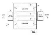
- Figure 1 shows a block diagram of a Doherty power amplifier 10 that includes a carrier amplifier 22 and a peaking amplifier 24 connected in parallel.
- the carrier amplifier 22 and peaking amplifier 24 are fabricated in a semiconductor package 20.
- An input signal 26 is split into two signals by an input splitter 28, which may apply a phase delay to one of the signals (e.g., a 90 degree phase delay).
- One of the resulting input signals is applied to a first input 32 of the carrier amplifier 22, and the other input signal is applied to a second input 36 of the peaking amplifier 24.
- the carrier amplifier 22 produces a first output signal at a first output 40 and the peaking amplifier 24 produces a second output signal at a second output 44.
- the first input 32 and the first output 40 may constitute a gate terminal and a drain terminal of the carrier amplifier 22, respectively; and the second input 36 and the second output 44 may constitute a gate terminal and a drain terminal of the peaking amplifier 24, respectively.
- the first and second output signals are combined through a power combiner 46 to produce a combined output signal 48.
- a Doherty power amplifier semiconductor package typically includes additional electronic devices and circuitry not shown herein for simplicity of illustration.
- the carrier amplifier 22 is configured to be active for an entire range of output powers of Doherty power amplifier 10.
- Peaking amplifier 24 is configured to turn on only when the carrier amplifier 22 saturates.
- Power combiner 46 operating to combine the first output signal from the carrier amplifier 22 with the second output signal from peaking amplifier 24, may include a quarter-wave impedance inverter.
- the quarter-wave impedance inverter can add a ninety degree lag to the output signal from the carrier amplifier 22 or the peaking amplifier 24 in order to compensate for the phase delay added by the input splitter to the signal provided to either the peaking amplifier 24 or the carrier amplifier.
- the phase of the signal provided to peaking amplifier 24 is typically designed to lag that of the carrier amplifier 22 by ninety degrees so that the two output signals add in-phase when the output signals are combined at the output of power combiner 46 to form combined output signal 48.
- each of the carrier amplifier 22 and peaking amplifier 24 may include a number of active and passive electrical elements.
- the carrier amplifier 22 may include a first capacitor that couples the first input 32 to a first transistor, which applies the appropriate amplification to the first input signal received at that input.
- An output of the first transistor can be connected to a second capacitor.
- the first and second capacitors operate to condition the input first signal that is amplified by the first transistor.
- the peaking amplifier 24 can include a third capacitor coupling the second input 36 to a second transistor, which applies the appropriate amplification to the second input signal received at the second input.
- An output of the second transistor can be connected to a fourth capacitor.
- the third and fourth capacitors operate to condition the input second signal that is amplified by the second transistor.
- the separate electrical devices making up the carrier amplifier 22 and the peaking amplifier 24 are connected to one another using multiple wires 72 and 73, known as wire bonds.
- wire bonds may be used to establish one or more of the signal paths of carrier amplifier 22 and peaking amplifier 24.
- the carrier amplifier 22 includes a number of electrical components, such as capacitors 60 and 64 and transistor 62 (having gate pad 63 and drain pad 65) manufactured and/or subsequently mounted to the surface of a common (i.e., single) carrier, such as a package ground plane 74.
- Capacitors 60 and 64 may be, for example, MOS capacitors mounted on ground plane 74.
- the peaking amplifier 24 includes a number of electrical devices, such as capacitors 66 and 70 and transistor 68 (having gate pad 69 and drain pad 71) manufactured on or subsequently mounted to the surface of a common (i.e., single) carrier, such as a package ground plane 74.
- Capacitors 66 and 70 may be, for example, Metal-Oxide-Semiconductor (MOS) capacitors mounted on ground plane 74.
- MOS Metal-Oxide-Semiconductor
- the symmetrical layout of the depicted semiconductor package 20 can result in the components of the carrier amplifier 22 being adjacent to corresponding components of the peaking amplifier 24. Accordingly, the arrangement of various components of each amplifier (including, specifically, the wire bonds 72 and 73 carrying high-frequency signals) are adjacent to and geometrically parallel with one another. These attributes of the wire bond arrays of the carrier and peaking amplifiers 22 and 24 can result in inductive coupling between the devices, which can reduce the performance of the overall circuit.
- an isolation wall 50 is formed between the carrier amplifier 22 and the peaking amplifier 24 to provide electrical isolation between the wire bonds arrays and other components of those amplifiers.
- the isolation wall 50 as described in greater detail below, is constructed as a body within the package between the circuitry of the carrier amplifier and the circuitry of the peaking amplifier.
- the material of the isolation wall 50 conducts, absorbs, or reflects electromagnetic emissions from either or both the carrier amplifier 22 or the peaking amplifier 24 preventing the emissions from reaching the other amplifier.
- the isolation wall 50 may be built on various substrates or a lead frame of the semiconductor package depending upon the particular package design implementation.
- the isolation wall 50 may be over molded with a conventional encapsulant or may be within an air-cavity package.
- the isolation wall 50 may be connected directly to a ground plane 74 or to a ground terminal which may, in turn be connected to a ground potential during operation of the Doherty power amplifier 10.
- the isolation wall 50 operates as a shield to interrupt and prevent the inductive coupling between the carrier amplifier and the peaking amplifier of the Doherty power amplifier 10.
- the isolation wall 50 may take any one of several forms, such as those which are being described in detail herein. Nevertheless, other wall configurations may be used to implement the present inventive concept.
- the isolation wall 50 is erected between the carrier amplifier 22 and the peaking amplifier 24 on the ground plane 74.
- the isolation wall 50 is positioned perpendicular to the ground plane 74 and extends some distance above a maximum height of the various components of the carrier amplifier 22 and peaking amplifier 24 (and their associated wire bonds).
- the isolation wall 50 may have a plurality of small holes 52 to allow the encapsulant to flow there through during the packaging process. The size of the holes 52 is sufficiently small so as not to adversely affect the electromagnetic isolation provided by the wall.
- an electrically conductive isolation wall 50 may be inserted into a slot or aperture 76 in the ground plane 74, thereby making electrical connection to that ground plane which is a ground node in the semiconductor device.
- Slot 76 may be formed within ground plane 74 by any suitable etching or material removal process.
- Figure 4 depicts an alternative isolation wall 79 having a bottom section that is bent to form a base 80 extending perpendicular to the main section 81 of the wall for supporting the isolation wall 79 on the surface of the ground plane 74.
- the base 80 may, in some cases, be used as a substitute for slot 76 in the ground plane as shown in Figure 4 .
- the base 80 is secured in a manner that establishes electrical contact with the ground plane 74, or ground node.
- the base 80 may be soldered, brazed, or attached by an electrically conductive adhesive or epoxy to the ground plane 74.
- either version of the conductive isolation wall 50 or 79 can be attached to a ground pad, a ground conductor, or other ground node of the circuitry within the semiconductor package 20.
- the isolation walls 50 and 79 extend upward within the encapsulant 77 and may be exposed through the top surface 78 of the housing 75 of the semiconductor package 20 as shown in Figure 5 .
- the edge of the wall 50 that is remote from the ground plane 74 may be spaced slightly from the top housing surface 78 so that some of the encapsulant 77 extends across that remote edge as shown in Figure 6 .
- the isolation wall 50 may be formed alternatively as part of the lead frame 82 of the semiconductor package 20.
- the lead frame 82 is fabricated in a convention manner from a flat electrically conductive sheet.
- the lead frame 82 has a plurality of lead fingers 84 and a pair of ground fingers 83 which will be connected to ground node in the semiconductor package 20.
- a wall section 85 is formed in the center of the lead frame 82 with serpentine links 86 at each end connecting the wall section to the pair of ground fingers 83.
- the wall section 85 is initially formed coplanar with the remainder 88 of the lead frame 82. Prior to assembly of the semiconductor package 20, the wall section 85 is bent transverse to the plane of the lead frame sheet as shown in Figures 8 and 9 .
- the wall section 85 is twisted by a particular amount (in some embodiments, approximately 90 degrees) about the links 86 into the desired final position of the isolation wall 50, which can be perpendicular to the plane of the remainder 88 of the lead frame sheet.
- the two links 87 connecting the wall section 85 to the pair of ground fingers 83 connects the resulting isolation wall 50 to ground or reference potential during operation of the Doherty power amplifier 10.
- the isolation wall 50 or 79 is fabricated on the ground plane 74 prior to encapsulation of the circuitry.
- Figure 10 depicts an alternative embodiment in which the conductive plane of the isolation wall 50 is fabricated after the circuitry has been encapsulated to form the semiconductor package 20.
- a slot 90 is formed through the top surface 92 of the package housing 95 into the encapsulation material.
- the slot 90 may be created by cutting the package with a blade, a saw, a laser beam, or similar device.
- the slot 90 extends downward through the encapsulation material between the carrier amplifier 22 and the peaking amplifier 24 until reaching the ground plane 74, the heat sink, or the die of the semiconductor device, whichever will provide a ground connection.
- a major surface of the slot 90 extending across the semiconductor package 20 is coated with an electrically conductive material 93 to form the isolation wall.
- an electrically conductive paint, epoxy, or other conductive material can be applied to one or more of the slot surfaces.
- at least one major slot surface may be plated with metal. That electrically conductive material 93 extends across the bottom of the slot 90 thereby making electrical contact with the ground plane 74, the heat sink, or the die of the semiconductor device to ground the conductive material 93 and form the isolation wall.
- Figure 11 illustrates another technique for forming the isolation wall in a slot 94 created in an encapsulated semiconductor package 20.
- an isolation wall 96 formed by a body of electrically conductive material, is inserted into the slot.
- a number of techniques can be employed to provide an electrical connection between the isolation wall 96 and either the ground plane of the circuit or a ground conductor on the circuit die.
- the die 97 may have a ground node 98 thereon and a plurality of wire bonds 99 extending between that ground node and ground terminals 100 of the semiconductor package 20.
- the slot 94 is cut into the semiconductor package 20 to a depth that just exposes the tops of the wire bonds 99 that connect to the ground node 98.
- the bottom edge of the body makes electrical contact with the exposed sections of the wire bonds 99 thereby grounding the isolation wall.
- the isolation wall 96 may be secured in the semiconductor package 20 by epoxy or other type of adhesive, for example.
- Figure 13 depicts a different technique for establishing electrical contact between the body of the isolation wall 96 and a ground node 98 within the semiconductor package 20.
- one or more electrically conductive posts 102 are attached to the ground node, such as a ground conductor of the semiconductor die 97 or the ground plane 74. These posts 102 become encapsulated in the material that forms the housing 95 of the semiconductor package 20.
- a slot 94 is formed in the package to a sufficient depth to expose the electrically conductive posts 102.
- the depth of the slot 94 in Figure 13 is not as critical as long as the posts 102 are exposed. Then, when the isolation wall 96 is inserted into the package housing 95, the lower edge of that wall contacts the exposed ends of the posts 102 thereby grounding the isolation wall. As with the prior embodiment, the isolation wall 96 can be secured within the slot 94 by epoxy or other type of adhesive, for example. Use of electrically conductive epoxy at the bottom of the slot 94 aids in making a ground connection to the posts 102.
- Figure 14 illustrates yet another technique for making an electrical contact between the isolation wall 96 and a ground node of electronic circuit in the semiconductor package 20.
- a plurality of vias 104 are formed between the bottom of the slot 94 and either a ground conductor on the die 97, the ground plane 74 or another ground node.
- the vias 104 are formed by cutting apertures through the encapsulant of the housing 95 between the bottom of the slot 94 and the respective ground node.
- An electrically conductive material such as a metal plating or conductive paint or other electrically conductive material, is applied to the walls of those apertures and then outward from the apertures across the bottom surface of the slot.
- the apertures can be filled with an electrically conductive material so as to form a structure similar to the posts 102.
- the isolation wall 96 when the isolation wall 96 is inserted into the slot 94, the bottom edge of that wall makes electrical contact with the vias 104 thereby connecting the wall to the circuit ground.
- electrically conductive epoxy at the bottom of the slot 94 to secure the isolation wall 96 in place also aids in making a ground connection to the vias 104.
- a semiconductor device in one embodiment, includes a substrate, a first circuit on the substrate and comprising a plurality of electrical components, and a second circuit on the substrate and comprising a plurality of electrical components.
- the semiconductor device includes an isolation wall formed of electrically conductive material located between the first circuit and the second circuit. The isolation wall is configured to reduce electromagnetic coupling between the first circuit and the second circuit during an operation of at least one of the first circuit and the second circuit.
- a Doherty amplifier in another embodiment, includes a substrate, a carrier amplifier on the substrate, and a peaking amplifier on the substrate adjacent to the carrier amplifier.
- the Doherty amplifier includes an isolation wall formed of electrically conductive material located between the carrier amplifier and the peaking amplifier. The isolation wall is configured to reduce an electromagnetic coupling between the carrier amplifier and the peaking amplifier during an operation of the Doherty amplifier.
- a method of fabricating a semiconductor device includes forming a first circuit on a substrate, and forming a second circuit on a substrate adjacent to the first circuit.
- the method includes locating an isolation wall of electrically conductive material between the first circuit and the second circuit.
- the isolation wall is configured to reduce electromagnetic coupling between the first circuit and the second circuit during an operation of the semiconductor device.
Landscapes
- Engineering & Computer Science (AREA)
- Power Engineering (AREA)
- Microelectronics & Electronic Packaging (AREA)
- Amplifiers (AREA)
- Physics & Mathematics (AREA)
- Health & Medical Sciences (AREA)
- Electromagnetism (AREA)
- Toxicology (AREA)
- Manufacturing & Machinery (AREA)
- Shielding Devices Or Components To Electric Or Magnetic Fields (AREA)
Abstract
Description
- The present disclosure relates generally to semiconductor device packages, and more specifically, to such packages incorporating a mechanism to reduce electromagnetic coupling between adjacent circuits therein.
- Wireless communication systems often employ power amplifiers for increasing the power of a signal. In a wireless communication system, a power amplifier is usually the last amplifier in a transmission chain (the output stage). High gain, high linearity, stability, and a high level of power-added efficiency (i.e., the ratio of the difference between the output power and the input power to DC power) are characteristics of an ideal amplifier.
- In general, a power amplifier operates at maximum power efficiency when the power amplifier transmits peak output power. However, power efficiency tends to worsen as output power decreases. Recently, Doherty power amplifier architecture has been the focus of attention not only for base stations, but also for mobile terminals because of the architecture's high power-added efficiency.
- A Doherty power amplifier includes two or more amplifiers, such as a carrier amplifier and a peaking amplifier. These amplifiers can be connected in parallel with their outputs joined by an offset transmission line, which performs impedance transformation. The peaking amplifier delivers current as the carrier amplifier saturates, thereby reducing the impedance seen at the output of the carrier amplifier. Thus, the carrier amplifier delivers more current to the load while the carrier amplifier is saturated because of a "load-pulling" effect. Since the carrier amplifier remains close to saturation, a Doherty power amplifier is able to transmit peak output power so that the total efficiency of the system remains relatively high.
- Such power amplifiers commonly are fabricated in a single semiconductor package. However, the circuit architecture presents challenges in terms of the semiconductor package design. Current Doherty power amplifier semiconductor package design calls for the use of discrete devices and integrated circuits that may involve one device that includes the carrier amplifier and a separate device that includes the peaking amplifier. These discrete devices are maintained a distance apart in the package in order to limit problems with crosstalk that can occur between the carrier and peaking amplifiers.
- Unfortunately, maintaining spatial distance between amplifiers in the package limits the potential for miniaturization of the semiconductor package. Limiting miniaturization is undesirable where low cost, a low weight, and a small volume are important package attributes for various applications.
- The present disclosure is illustrated by way of examples and embodiments and is not limited by the accompanying figures, in which like reference numbers indicate similar elements. For simplicity and clarity of illustration, the drawing figures illustrate the general manner of construction, and descriptions and details of well-known features and techniques may be omitted to avoid unnecessarily obscuring the invention. Elements in the figures are illustrated for simplicity and clarity and have not necessarily been drawn to scale. In fact, the dimensions of some of the elements or regions in the figures may be exaggerated relative to other elements or regions to improve understanding of embodiments of apparatus. The figures along with the detailed description are incorporated and form part of the specification and serve to further illustrate examples, embodiments and the like, and explain various principles and advantages, in accordance with the present disclosure, where:
-
FIGURE 1 is a block diagram of an example embodiment of a Doherty power amplifier in a semiconductor package with an isolation wall. -
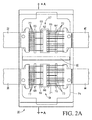
FIGURE 2A is a top schematic view of components of the carrier and peaking amplifiers for an example embodiment of a Doherty power amplifier in a semiconductor package. -
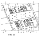
FIGURE 2B is a perspective view of the Doherty power amplifier components in the semiconductor package ofFigure 2A . -
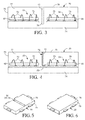
FIGURE 3 is a cross section view taken along line A-A inFigure 2A showing one embodiment of the isolation wall. -
FIGURE 4 is a cross section view taken along line A-A inFigure 2A illustrating another embodiment of the isolation wall. -
FIGURES 5 and 6 are perspective views of two embodiments of a completed semiconductor package with the circuitry encapsulated in a resin body. -
FIGURE 7 is a top view of an embodiment of a lead frame for a semiconductor package with the isolation wall formed by part of the lead frame. -
FIGURE 8 is a top view of the lead frame ofFigure 7 with the isolation wall bent upward into a final position. -
FIGURE 9 is a side view of the lead frame ofFigure 7 with the bent isolation wall. -
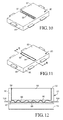
FIGURE 10 is a perspective view of a completed semiconductor package with a slot created therein and another embodiment of an isolation wall formed in the slot. -
FIGURE 11 is a perspective view of a completed semiconductor package with a slot created therein and an isolation wall inserted into the slot according to another embodiment. -
FIGURE 12 is a cross section view taken along line B-B inFigure 11 showing a first manner of connecting the isolation wall to ground. -
FIGURE 13 is a cross section view taken along line B-B inFigure 11 showing a second manner of connecting the isolation wall to ground. -
FIGURE 14 is a cross section view taken along line B-B inFigure 11 showing a third manner of connecting the isolation wall to ground. - The following detailed description is exemplary in nature and is not intended to limit the invention or the application and uses of the same. Furthermore, there is no intention to be bound by any expressed or implied theory presented in the preceding technical field, background, or the following detailed description.
- The terms "first," "second," "third," "fourth" and the like in the description and the claims, if any, may be used for distinguishing between similar elements and not necessarily for describing a particular sequential or chronological order. It is to be understood that the terms so used are interchangeable under appropriate circumstances such that the embodiments of the invention described herein are, for example, capable of operation in sequences other than those illustrated or otherwise described herein. Reference herein to directional relationships, such as top and bottom or left and right, refer to the relationship of the components in the orientation illustrated in the drawings, which may not be the orientation of the components in all uses of the apparatus being described. Furthermore, the terms "comprise," "include," "have" and any variations thereof, are intended to cover non-exclusive inclusions, such that a process, method, article, or apparatus that comprises a list of elements is not necessarily limited to those elements, but may include other elements not expressly listed or inherent to such process, method, article, or apparatus. The term "coupled," as used herein, is defined as directly or indirectly connected in an electrical or non-electrical manner. The terms "substantial" and "substantially" herein mean sufficient to accomplish the stated purpose in a practical manner and that minor imperfections, if any, are not significant for the stated purpose.
- The present embodiments may be used to improve the usability of a power amplifier semiconductor package in base station power amplifiers, cell phones, other portable devices, and other apparatus dependent upon semiconductor packages, where low cost, low weight, and small volume are desired. The embodiments described herein may reduce inductive coupling between components and wire bond arrays in a multipath power amplifier (including but not limited to Doherty power amplifiers). However, it will become apparent that the techniques described below for reducing inductive coupling and electromagnetic interference may be implemented in a variety of semiconductor device designs and other circuits.
-
Figure 1 shows a block diagram of a Dohertypower amplifier 10 that includes acarrier amplifier 22 and apeaking amplifier 24 connected in parallel. Thecarrier amplifier 22 and peakingamplifier 24 are fabricated in asemiconductor package 20. Aninput signal 26 is split into two signals by aninput splitter 28, which may apply a phase delay to one of the signals (e.g., a 90 degree phase delay). One of the resulting input signals is applied to afirst input 32 of thecarrier amplifier 22, and the other input signal is applied to asecond input 36 of thepeaking amplifier 24. Thecarrier amplifier 22 produces a first output signal at afirst output 40 and thepeaking amplifier 24 produces a second output signal at asecond output 44. In a Doherty configuration, thefirst input 32 and thefirst output 40 may constitute a gate terminal and a drain terminal of thecarrier amplifier 22, respectively; and thesecond input 36 and thesecond output 44 may constitute a gate terminal and a drain terminal of thepeaking amplifier 24, respectively. The first and second output signals are combined through a power combiner 46 to produce a combinedoutput signal 48. Those skilled in the art will recognize that a Doherty power amplifier semiconductor package typically includes additional electronic devices and circuitry not shown herein for simplicity of illustration. - In one embodiment, the
carrier amplifier 22 is configured to be active for an entire range of output powers of Dohertypower amplifier 10.Peaking amplifier 24 is configured to turn on only when thecarrier amplifier 22 saturates. Power combiner 46, operating to combine the first output signal from thecarrier amplifier 22 with the second output signal frompeaking amplifier 24, may include a quarter-wave impedance inverter. The quarter-wave impedance inverter can add a ninety degree lag to the output signal from thecarrier amplifier 22 or thepeaking amplifier 24 in order to compensate for the phase delay added by the input splitter to the signal provided to either thepeaking amplifier 24 or the carrier amplifier. The phase of the signal provided to peakingamplifier 24 is typically designed to lag that of thecarrier amplifier 22 by ninety degrees so that the two output signals add in-phase when the output signals are combined at the output of power combiner 46 to form combinedoutput signal 48. - In the exemplary circuit in
Figure 1 , each of thecarrier amplifier 22 and peakingamplifier 24 may include a number of active and passive electrical elements. For example, thecarrier amplifier 22 may include a first capacitor that couples thefirst input 32 to a first transistor, which applies the appropriate amplification to the first input signal received at that input. An output of the first transistor can be connected to a second capacitor. The first and second capacitors operate to condition the input first signal that is amplified by the first transistor. Similarly, the peakingamplifier 24 can include a third capacitor coupling thesecond input 36 to a second transistor, which applies the appropriate amplification to the second input signal received at the second input. An output of the second transistor can be connected to a fourth capacitor. The third and fourth capacitors operate to condition the input second signal that is amplified by the second transistor. Those skilled in the art will recognize that thecarrier amplifier 22 and peakingamplifier 24 may include additional electronic components not shown herein for simplicity of illustration. - With reference to the
semiconductor package 20 inFigures 2A and2B , the separate electrical devices making up thecarrier amplifier 22 and the peakingamplifier 24 are connected to one another usingmultiple wires carrier amplifier 22 may be established using wire bonds. Likewise, wire bonds may be used to establish one or more of the signal paths ofcarrier amplifier 22 and peakingamplifier 24. - The
carrier amplifier 22 includes a number of electrical components, such ascapacitors gate pad 63 and drain pad 65) manufactured and/or subsequently mounted to the surface of a common (i.e., single) carrier, such as apackage ground plane 74.Capacitors ground plane 74. Similarly, the peakingamplifier 24 includes a number of electrical devices, such ascapacitors gate pad 69 and drain pad 71) manufactured on or subsequently mounted to the surface of a common (i.e., single) carrier, such as apackage ground plane 74.Capacitors ground plane 74. - The symmetrical layout of the depicted
semiconductor package 20 can result in the components of thecarrier amplifier 22 being adjacent to corresponding components of the peakingamplifier 24. Accordingly, the arrangement of various components of each amplifier (including, specifically, thewire bonds amplifiers - Therefore, in the
present semiconductor package 20 for components of aDoherty power amplifier 10, anisolation wall 50 is formed between thecarrier amplifier 22 and the peakingamplifier 24 to provide electrical isolation between the wire bonds arrays and other components of those amplifiers. Theisolation wall 50, as described in greater detail below, is constructed as a body within the package between the circuitry of the carrier amplifier and the circuitry of the peaking amplifier. The material of theisolation wall 50 conducts, absorbs, or reflects electromagnetic emissions from either or both thecarrier amplifier 22 or the peakingamplifier 24 preventing the emissions from reaching the other amplifier. Theisolation wall 50 may be built on various substrates or a lead frame of the semiconductor package depending upon the particular package design implementation. Along with the other components in thesemiconductor package 20, theisolation wall 50 may be over molded with a conventional encapsulant or may be within an air-cavity package. In various implementations, theisolation wall 50 may be connected directly to aground plane 74 or to a ground terminal which may, in turn be connected to a ground potential during operation of theDoherty power amplifier 10. In general, theisolation wall 50 operates as a shield to interrupt and prevent the inductive coupling between the carrier amplifier and the peaking amplifier of theDoherty power amplifier 10. - The
isolation wall 50 may take any one of several forms, such as those which are being described in detail herein. Nevertheless, other wall configurations may be used to implement the present inventive concept. - With particular reference to
Figure 2B , theisolation wall 50 is erected between thecarrier amplifier 22 and the peakingamplifier 24 on theground plane 74. According to various embodiments, theisolation wall 50 is positioned perpendicular to theground plane 74 and extends some distance above a maximum height of the various components of thecarrier amplifier 22 and peaking amplifier 24 (and their associated wire bonds). In the situation in which the electronic circuit is encapsulated to form ahousing 75 of the semiconductor package 20 (seeFigures 5 and 6 ), theisolation wall 50 may have a plurality ofsmall holes 52 to allow the encapsulant to flow there through during the packaging process. The size of theholes 52 is sufficiently small so as not to adversely affect the electromagnetic isolation provided by the wall. As shown inFigure 3 , an electricallyconductive isolation wall 50 may be inserted into a slot oraperture 76 in theground plane 74, thereby making electrical connection to that ground plane which is a ground node in the semiconductor device.Slot 76 may be formed withinground plane 74 by any suitable etching or material removal process. -
Figure 4 depicts analternative isolation wall 79 having a bottom section that is bent to form abase 80 extending perpendicular to themain section 81 of the wall for supporting theisolation wall 79 on the surface of theground plane 74. The base 80 may, in some cases, be used as a substitute forslot 76 in the ground plane as shown inFigure 4 . Thebase 80 is secured in a manner that establishes electrical contact with theground plane 74, or ground node. For example, thebase 80 may be soldered, brazed, or attached by an electrically conductive adhesive or epoxy to theground plane 74. Alternatively, either version of theconductive isolation wall semiconductor package 20. - The
isolation walls encapsulant 77 and may be exposed through thetop surface 78 of thehousing 75 of thesemiconductor package 20 as shown inFigure 5 . Alternatively, the edge of thewall 50 that is remote from theground plane 74 may be spaced slightly from thetop housing surface 78 so that some of theencapsulant 77 extends across that remote edge as shown inFigure 6 . - With reference to
Figure 7 , theisolation wall 50 may be formed alternatively as part of thelead frame 82 of thesemiconductor package 20. Thelead frame 82 is fabricated in a convention manner from a flat electrically conductive sheet. Thelead frame 82 has a plurality oflead fingers 84 and a pair ofground fingers 83 which will be connected to ground node in thesemiconductor package 20. Awall section 85 is formed in the center of thelead frame 82 withserpentine links 86 at each end connecting the wall section to the pair ofground fingers 83. Thewall section 85 is initially formed coplanar with theremainder 88 of thelead frame 82. Prior to assembly of thesemiconductor package 20, thewall section 85 is bent transverse to the plane of the lead frame sheet as shown inFigures 8 and 9 . Specifically thewall section 85 is twisted by a particular amount (in some embodiments, approximately 90 degrees) about thelinks 86 into the desired final position of theisolation wall 50, which can be perpendicular to the plane of theremainder 88 of the lead frame sheet. The two links 87 connecting thewall section 85 to the pair ofground fingers 83 connects the resultingisolation wall 50 to ground or reference potential during operation of theDoherty power amplifier 10. - In the embodiments of the
semiconductor package 20 described thus far, theisolation wall ground plane 74 prior to encapsulation of the circuitry.Figure 10 depicts an alternative embodiment in which the conductive plane of theisolation wall 50 is fabricated after the circuitry has been encapsulated to form thesemiconductor package 20. After encapsulation, aslot 90 is formed through thetop surface 92 of thepackage housing 95 into the encapsulation material. For example, theslot 90 may be created by cutting the package with a blade, a saw, a laser beam, or similar device. Theslot 90 extends downward through the encapsulation material between thecarrier amplifier 22 and the peakingamplifier 24 until reaching theground plane 74, the heat sink, or the die of the semiconductor device, whichever will provide a ground connection. - Then a major surface of the
slot 90 extending across thesemiconductor package 20 is coated with an electricallyconductive material 93 to form the isolation wall. For example, an electrically conductive paint, epoxy, or other conductive material can be applied to one or more of the slot surfaces. Alternatively at least one major slot surface may be plated with metal. That electricallyconductive material 93 extends across the bottom of theslot 90 thereby making electrical contact with theground plane 74, the heat sink, or the die of the semiconductor device to ground theconductive material 93 and form the isolation wall. -
Figure 11 illustrates another technique for forming the isolation wall in aslot 94 created in an encapsulatedsemiconductor package 20. After theslot 94 is formed in thesemiconductor package 20, anisolation wall 96, formed by a body of electrically conductive material, is inserted into the slot. A number of techniques can be employed to provide an electrical connection between theisolation wall 96 and either the ground plane of the circuit or a ground conductor on the circuit die. For example, as shown inFigure 12 , thedie 97 may have aground node 98 thereon and a plurality ofwire bonds 99 extending between that ground node andground terminals 100 of thesemiconductor package 20. In this embodiment, theslot 94 is cut into thesemiconductor package 20 to a depth that just exposes the tops of thewire bonds 99 that connect to theground node 98. As a result, when the body of theisolation wall 96 is inserted in theslot 94, the bottom edge of the body makes electrical contact with the exposed sections of thewire bonds 99 thereby grounding the isolation wall. Theisolation wall 96 may be secured in thesemiconductor package 20 by epoxy or other type of adhesive, for example. -
Figure 13 depicts a different technique for establishing electrical contact between the body of theisolation wall 96 and aground node 98 within thesemiconductor package 20. Here, prior to encapsulation, one or more electricallyconductive posts 102 are attached to the ground node, such as a ground conductor of the semiconductor die 97 or theground plane 74. Theseposts 102 become encapsulated in the material that forms thehousing 95 of thesemiconductor package 20. During or after encapsulation, aslot 94 is formed in the package to a sufficient depth to expose the electricallyconductive posts 102. Unlike the use ofwire bonds 99 inFigure 12 , where care must be taken so that the slot is not cut so deep as to sever the wire bonds, the depth of theslot 94 inFigure 13 is not as critical as long as theposts 102 are exposed. Then, when theisolation wall 96 is inserted into thepackage housing 95, the lower edge of that wall contacts the exposed ends of theposts 102 thereby grounding the isolation wall. As with the prior embodiment, theisolation wall 96 can be secured within theslot 94 by epoxy or other type of adhesive, for example. Use of electrically conductive epoxy at the bottom of theslot 94 aids in making a ground connection to theposts 102. -
Figure 14 illustrates yet another technique for making an electrical contact between theisolation wall 96 and a ground node of electronic circuit in thesemiconductor package 20. In this instance, after theslot 94 is cut in thehousing 95, a plurality ofvias 104 are formed between the bottom of theslot 94 and either a ground conductor on thedie 97, theground plane 74 or another ground node. Specifically thevias 104 are formed by cutting apertures through the encapsulant of thehousing 95 between the bottom of theslot 94 and the respective ground node. An electrically conductive material, such as a metal plating or conductive paint or other electrically conductive material, is applied to the walls of those apertures and then outward from the apertures across the bottom surface of the slot. Alternatively, the apertures can be filled with an electrically conductive material so as to form a structure similar to theposts 102. In both these instances, when theisolation wall 96 is inserted into theslot 94, the bottom edge of that wall makes electrical contact with thevias 104 thereby connecting the wall to the circuit ground. Use of electrically conductive epoxy at the bottom of theslot 94 to secure theisolation wall 96 in place also aids in making a ground connection to thevias 104. - The techniques shown in
Figures 12-14 for establishing electrical contact with the isolation wall also can be used when the wall is formed by a coating on a surface of the slot in thesemiconductor package 20 as illustrated inFigure 10 . - Although embodiments have been described herein with respect to a Doherty power amplifier with one carrier amplifier and one peaking amplifier, those of skill in the art would understand, based on the description herein, that embodiments of the inventive subject matter may be used in conjunction with virtually any type of multiple path amplifier. Accordingly, the various embodiments are not limited to use with Doherty amplifiers, nor are they limited to use with amplifiers having only two amplification paths. For example, an alternate embodiment may include a device with three or more amplification paths, and isolation walls may be provided between each set of adjacent amplification paths. In addition, although various embodiments have been described with respect to overmolded (encapsulated) semiconductor device packages, the inventive concepts also could be applied to air cavity packages and other types of packages.
- In one embodiment, a semiconductor device includes a substrate, a first circuit on the substrate and comprising a plurality of electrical components, and a second circuit on the substrate and comprising a plurality of electrical components. The semiconductor device includes an isolation wall formed of electrically conductive material located between the first circuit and the second circuit. The isolation wall is configured to reduce electromagnetic coupling between the first circuit and the second circuit during an operation of at least one of the first circuit and the second circuit.
- In another embodiment, a Doherty amplifier includes a substrate, a carrier amplifier on the substrate, and a peaking amplifier on the substrate adjacent to the carrier amplifier. The Doherty amplifier includes an isolation wall formed of electrically conductive material located between the carrier amplifier and the peaking amplifier. The isolation wall is configured to reduce an electromagnetic coupling between the carrier amplifier and the peaking amplifier during an operation of the Doherty amplifier.
- In another embodiment, a method of fabricating a semiconductor device includes forming a first circuit on a substrate, and forming a second circuit on a substrate adjacent to the first circuit. The method includes locating an isolation wall of electrically conductive material between the first circuit and the second circuit. The isolation wall is configured to reduce electromagnetic coupling between the first circuit and the second circuit during an operation of the semiconductor device.
- The foregoing description was primarily directed to a preferred embodiment of the invention. Although some attention was given to various alternatives within the scope of the invention, it is anticipated that one skilled in the art will likely realize additional alternatives that are now apparent from disclosure of embodiments of the invention. Accordingly, the scope of the invention should be determined from the following claims and not limited by the above disclosure.
Claims (15)
- A semiconductor device (10) comprising:a substrate;a first circuit (22) on the substrate and comprising a plurality of electrical components;a second circuit (24) on the substrate and comprising a plurality of electrical components; andan isolation wall (50) formed of electrically conductive material located between the first circuit (22) and the second circuit (24), the isolation wall (50) being configured to reduce electromagnetic coupling between the first circuit (22) and the second circuit (24) during an operation of at least one of the first circuit (22) and the second circuit (24);wherein the isolation wall (50) includes a plurality of holes (52) through which encapsulation material may flow during a process of making the semiconductor device (10).
- The semiconductor device (10) as recited in claim 1, further comprising a ground potential node (83), wherein the isolation wall (50) is electrically connected to the ground potential node (83).
- The semiconductor device (10) as recited in claim 2, wherein the isolation wall (50) is electrically connected to the ground potential node (83) by one of solder, brazing material, and adhesive.
- The semiconductor device (10) as recited in claim 2 or 3, wherein the isolation wall (50) is received within an aperture (76) in the ground potential node (83).
- The semiconductor device (10) as recited in any one of the preceding claims, wherein the isolation wall (50) is formed by a section of a lead frame (82) for the semiconductor device (10).
- The semiconductor device (10) as recited in any one of the preceding claims, further comprising a housing encapsulating (77) the substrate, the first circuit (22), and the second circuit (24).
- The semiconductor device (10) as recited in any one of the preceding claims, further comprising:a ground plane (74); andthe isolation wall (50) being positioned perpendicular to the ground plane (74) and extending above a maximum height of components of the first circuit (22) and the second circuit (24) and wire bonds associated with each of the first circuit (22) and the second circuit (24).
- The semiconductor device (10) as recited in any one of the preceding claims, wherein the first electrical circuit is a carrier amplifier (22) of a Doherty amplifier; and the second electrical circuit is a peaking amplifier (24) of the Doherty amplifier.
- A method of fabricating a semiconductor device (10), the method comprising:forming a first circuit (22) on a substrate;forming a second circuit (24) on a substrate adjacent to the first circuit (22); andlocating an isolation wall (50) of electrically conductive material between the first circuit (22) and the second circuit (24), the isolation wall (50) being configured to reduce electromagnetic coupling between the first circuit (22) and the second circuit (24) during an operation of the semiconductor device (10),wherein the isolation wall (50) includes a plurality of holes (52) through which encapsulation material may flow during a process of making the semiconductor device (10).
- The method as recited in claim 9, wherein locating an isolation wall (50) comprises forming a lead frame from an electrically conductive sheet, wherein a wall section is defined in the electrically conductive sheet; and bending the wall section transverse to the electrically conductive sheet thereby forming the isolation wall (50).
- The method as recited in claim 9 or 10, further comprising encapsulating (77) the substrate, the first circuit (22), and the second circuit (24) in a body of material.
- The method as recited in claim 9, further comprising inserting the isolation wall (50) into a slot or aperture (76) in a ground plane (74) of the semiconductor device (10).
- The method as recited in claim 9, further comprising providing a ground potential node (83), and electrically connecting the isolation wall (50) to the ground potential node (83) by one of solder, brazing material, and adhesive.
- The method as recited in claim 9, further comprising forming the isolation wall (50) by a section of a lead frame (82) for the semiconductor device (10).
- The method as recited in claim 9, further comprising:providing a ground plane (74); andpositioning the isolation wall (50) perpendicular to the ground plane (74), the isolation wall (50) extending above a maximum height of components of the first circuit (22) and the second circuit (24) and wire bonds associated with each of the first circuit (22) and the second circuit (24).
Applications Claiming Priority (2)
| Application Number | Priority Date | Filing Date | Title |
|---|---|---|---|
| US14/104,870 US9450547B2 (en) | 2013-12-12 | 2013-12-12 | Semiconductor package having an isolation wall to reduce electromagnetic coupling |
| EP14196131.8A EP2892076A3 (en) | 2013-12-12 | 2014-12-03 | Semiconductor package having an isolation wall to reduce electromagnetic coupling |
Related Parent Applications (1)
| Application Number | Title | Priority Date | Filing Date |
|---|---|---|---|
| EP14196131.8A Division EP2892076A3 (en) | 2013-12-12 | 2014-12-03 | Semiconductor package having an isolation wall to reduce electromagnetic coupling |
Publications (1)
| Publication Number | Publication Date |
|---|---|
| EP3151273A1 true EP3151273A1 (en) | 2017-04-05 |
Family
ID=52347074
Family Applications (2)
| Application Number | Title | Priority Date | Filing Date |
|---|---|---|---|
| EP16194094.5A Withdrawn EP3151273A1 (en) | 2013-12-12 | 2014-12-03 | Semiconductor package having an isolation wall |
| EP14196131.8A Ceased EP2892076A3 (en) | 2013-12-12 | 2014-12-03 | Semiconductor package having an isolation wall to reduce electromagnetic coupling |
Family Applications After (1)
| Application Number | Title | Priority Date | Filing Date |
|---|---|---|---|
| EP14196131.8A Ceased EP2892076A3 (en) | 2013-12-12 | 2014-12-03 | Semiconductor package having an isolation wall to reduce electromagnetic coupling |
Country Status (4)
| Country | Link |
|---|---|
| US (4) | US9450547B2 (en) |
| EP (2) | EP3151273A1 (en) |
| JP (1) | JP2015115960A (en) |
| CN (1) | CN104716107B (en) |
Families Citing this family (42)
| Publication number | Priority date | Publication date | Assignee | Title |
|---|---|---|---|---|
| US9312817B2 (en) | 2012-07-20 | 2016-04-12 | Freescale Semiconductor, Inc. | Semiconductor package design providing reduced electromagnetic coupling between circuit components |
| US9240390B2 (en) | 2013-06-27 | 2016-01-19 | Freescale Semiconductor, Inc. | Semiconductor packages having wire bond wall to reduce coupling |
| US9401342B2 (en) * | 2013-06-27 | 2016-07-26 | Freescale Semiconductor, Inc. | Semiconductor package having wire bond wall to reduce coupling |
| US9450547B2 (en) * | 2013-12-12 | 2016-09-20 | Freescale Semiconductor, Inc. | Semiconductor package having an isolation wall to reduce electromagnetic coupling |
| JP6550738B2 (en) * | 2013-12-18 | 2019-07-31 | Tdk株式会社 | High frequency amplifier |
| JP6017492B2 (en) * | 2014-04-24 | 2016-11-02 | Towa株式会社 | Manufacturing method of resin-encapsulated electronic component, plate-like member with protruding electrode, and resin-encapsulated electronic component |
| JP5944445B2 (en) | 2014-07-18 | 2016-07-05 | Towa株式会社 | Manufacturing method of resin-encapsulated electronic component, plate-like member with protruding electrode, resin-encapsulated electronic component, and manufacturing method of plate-like member with protruding electrode |
| US9986646B2 (en) | 2014-11-21 | 2018-05-29 | Nxp Usa, Inc. | Packaged electronic devices with top terminations, and methods of manufacture thereof |
| US9986639B2 (en) * | 2015-06-29 | 2018-05-29 | Analog Devices Global | Vertical magnetic barrier for integrated electronic module and related methods |
| JP6332565B2 (en) | 2015-09-01 | 2018-05-30 | 日本電気株式会社 | Power amplification apparatus and television signal transmission system |
| US9607953B1 (en) * | 2016-02-24 | 2017-03-28 | Nxp Usa, Inc. | Semiconductor package with isolation wall |
| US9831835B2 (en) | 2016-02-26 | 2017-11-28 | Nxp Usa, Inc. | Multiple path amplifier with pre-cancellation |
| CN107197618B (en) * | 2016-03-15 | 2020-06-26 | 中兴通讯股份有限公司 | Radio frequency shielding box, power amplifier and radio frequency shielding method |
| US10249582B2 (en) | 2016-12-19 | 2019-04-02 | Nxp Usa, Inc. | Radio frequency (RF) devices with resonant circuits to reduce coupling |
| US10083899B2 (en) | 2017-01-23 | 2018-09-25 | Infineon Technologies Ag | Semiconductor package with heat slug and rivet free die attach area |
| US10381321B2 (en) * | 2017-02-18 | 2019-08-13 | Kulicke And Soffa Industries, Inc | Ultrasonic transducer systems including tuned resonators, equipment including such systems, and methods of providing the same |
| JP2019092009A (en) | 2017-11-13 | 2019-06-13 | 住友電気工業株式会社 | Semiconductor amplification element and semiconductor amplification device |
| JP2019176281A (en) * | 2018-03-28 | 2019-10-10 | 住友電気工業株式会社 | Amplifier and Doherty amplifier circuit |
| US11127689B2 (en) | 2018-06-01 | 2021-09-21 | Qorvo Us, Inc. | Segmented shielding using wirebonds |
| US11219144B2 (en) | 2018-06-28 | 2022-01-04 | Qorvo Us, Inc. | Electromagnetic shields for sub-modules |
| US10763334B2 (en) | 2018-07-11 | 2020-09-01 | Cree, Inc. | Drain and/or gate interconnect and finger structure |
| US10600746B2 (en) | 2018-07-19 | 2020-03-24 | Cree, Inc. | Radio frequency transistor amplifiers and other multi-cell transistors having gaps and/or isolation structures between groups of unit cell transistors |
| KR102564085B1 (en) * | 2018-08-20 | 2023-08-04 | 미쓰비시덴키 가부시키가이샤 | doherty amplifier |
| US10506704B1 (en) | 2018-08-21 | 2019-12-10 | Nxp Usa, Inc. | Electromagnetically-shielded microelectronic assemblies and methods for the fabrication thereof |
| EP3624186B1 (en) * | 2018-08-21 | 2021-11-03 | NXP USA, Inc. | Electromagnetically-shielded microelectronic assemblies |
| US10629518B2 (en) * | 2018-08-29 | 2020-04-21 | Nxp Usa, Inc. | Internally-shielded microelectronic packages and methods for the fabrication thereof |
| CN109413301B (en) * | 2018-12-05 | 2020-12-22 | 贵州航天电子科技有限公司 | Small video amplifier combination structure |
| US11114363B2 (en) | 2018-12-20 | 2021-09-07 | Qorvo Us, Inc. | Electronic package arrangements and related methods |
| US11417746B2 (en) | 2019-04-24 | 2022-08-16 | Wolfspeed, Inc. | High power transistor with interior-fed fingers |
| US11515282B2 (en) | 2019-05-21 | 2022-11-29 | Qorvo Us, Inc. | Electromagnetic shields with bonding wires for sub-modules |
| US11011813B2 (en) * | 2019-07-12 | 2021-05-18 | Nxp B.V. | Power amplifier with shielded transmission lines |
| US11258356B2 (en) | 2019-07-31 | 2022-02-22 | Analog Devices International Unlimited Company | Magnetic barrier for power module |
| US20220415763A1 (en) | 2019-11-29 | 2022-12-29 | Ampleon Netherlands B.V. | Lead Frame Based Molded Radio Frequency Package |
| US11349438B2 (en) | 2019-12-30 | 2022-05-31 | Nxp Usa, Inc. | Power amplifier packages containing multi-path integrated passive devices |
| JP7306289B2 (en) * | 2020-02-10 | 2023-07-11 | 住友電気工業株式会社 | semiconductor devices and amplifiers |
| US11121072B1 (en) | 2020-03-16 | 2021-09-14 | Nxp Usa, Inc. | Semiconductor device with isolation structure |
| US11990872B2 (en) * | 2020-04-17 | 2024-05-21 | Nxp Usa, Inc. | Power amplifier modules including topside cooling interfaces and methods for the fabrication thereof |
| US11581859B2 (en) | 2020-06-26 | 2023-02-14 | Wolfspeed, Inc. | Radio frequency (RF) transistor amplifier packages with improved isolation and lead configurations |
| US11342275B2 (en) * | 2020-10-22 | 2022-05-24 | Nxp Usa, Inc. | Leadless power amplifier packages including topside terminations and methods for the fabrication thereof |
| US11984429B2 (en) | 2021-09-30 | 2024-05-14 | Nxp Usa, Inc. | Leadless power amplifier packages including topside termination interposer arrangements and methods for the fabrication thereof |
| WO2025013098A1 (en) * | 2023-07-13 | 2025-01-16 | Jio Platforms Limited | System and method for providing high powered 5g nr integrated macro gnodeb |
| WO2025146744A1 (en) * | 2024-01-05 | 2025-07-10 | 株式会社村田製作所 | Power amplification circuit and power amplification device |
Citations (4)
| Publication number | Priority date | Publication date | Assignee | Title |
|---|---|---|---|---|
| WO2006008679A2 (en) * | 2004-07-13 | 2006-01-26 | Koninklijke Philips Electronics N.V. | Electronic device comprising an integrated circuit |
| US7629674B1 (en) * | 2004-11-17 | 2009-12-08 | Amkor Technology, Inc. | Shielded package having shield fence |
| EP2584605A2 (en) * | 2011-10-21 | 2013-04-24 | Huawei Device Co., Ltd. | Packaging structure and method and electronic device |
| WO2013179382A1 (en) * | 2012-05-29 | 2013-12-05 | 日本電気株式会社 | Plural system amplification device |
Family Cites Families (44)
| Publication number | Priority date | Publication date | Assignee | Title |
|---|---|---|---|---|
| US3500440A (en) | 1968-01-08 | 1970-03-10 | Interamericano Projects Inc | Functional building blocks facilitating mass production of electronic equipment by unskilled labor |
| JPS49131863U (en) | 1973-03-10 | 1974-11-13 | ||
| US4370700A (en) | 1980-06-03 | 1983-01-25 | Motorola Inc. | RF Package including RF shielding for a multiple PC board |
| US5068708A (en) | 1989-10-02 | 1991-11-26 | Advanced Micro Devices, Inc. | Ground plane for plastic encapsulated integrated circuit die packages |
| US5191544A (en) * | 1990-06-15 | 1993-03-02 | International Business Machines Corp. | Personal computer enclosure with shielding |
| US5222294A (en) * | 1990-12-03 | 1993-06-29 | Motorola, Inc. | High isolation packaging method |
| US5261868A (en) | 1992-04-14 | 1993-11-16 | Pryor Jr Joe E | Exercise device |
| KR100306988B1 (en) | 1992-10-26 | 2001-12-15 | 윌리엄 비. 켐플러 | Device Package |
| US5482898A (en) | 1993-04-12 | 1996-01-09 | Amkor Electronics, Inc. | Method for forming a semiconductor device having a thermal dissipator and electromagnetic shielding |
| US5557063A (en) * | 1994-01-03 | 1996-09-17 | Lucent Technologies Inc. | Electronic component enclosure for RF shielding |
| US5608188A (en) * | 1994-09-02 | 1997-03-04 | Motorola, Inc. | Multi compartment electromagnetic energy shield |
| JPH0982880A (en) * | 1995-09-13 | 1997-03-28 | Toyota Autom Loom Works Ltd | Lead frame and semiconductor device |
| US5661337A (en) | 1995-11-07 | 1997-08-26 | Vlsi Technology, Inc. | Technique for improving bonding strength of leadframe to substrate in semiconductor IC chip packages |
| JPH10200349A (en) * | 1997-01-13 | 1998-07-31 | Yokowo Co Ltd | Low noise amplifier and on-vehicle antenna provided with the same |
| JPH11158448A (en) * | 1997-11-28 | 1999-06-15 | Sony Corp | Conductive adhesive and electronic component using the same |
| US6121546A (en) * | 1998-04-20 | 2000-09-19 | Lucent Technologies Inc. | RF shield |
| US6261868B1 (en) | 1999-04-02 | 2001-07-17 | Motorola, Inc. | Semiconductor component and method for manufacturing the semiconductor component |
| JP3505488B2 (en) * | 1999-10-12 | 2004-03-08 | 古河電気工業株式会社 | Optical module |
| US6614102B1 (en) | 2001-05-04 | 2003-09-02 | Amkor Technology, Inc. | Shielded semiconductor leadframe package |
| US6873529B2 (en) | 2002-02-26 | 2005-03-29 | Kyocera Corporation | High frequency module |
| WO2005011114A1 (en) | 2003-07-29 | 2005-02-03 | Matsushita Electric Industrial Co., Ltd. | Surface acoustic wave device |
| US7075174B2 (en) | 2004-02-26 | 2006-07-11 | Agere Systems Inc. | Semiconductor packaging techniques for use with non-ceramic packages |
| US7432586B2 (en) | 2004-06-21 | 2008-10-07 | Broadcom Corporation | Apparatus and method for thermal and electromagnetic interference (EMI) shielding enhancement in die-up array packages |
| US7445967B2 (en) | 2006-01-20 | 2008-11-04 | Freescale Semiconductor, Inc. | Method of packaging a semiconductor die and package thereof |
| JP4789648B2 (en) * | 2006-02-21 | 2011-10-12 | 富士通株式会社 | Enclosure for information technology equipment |
| US7463496B2 (en) | 2006-03-09 | 2008-12-09 | Laird Technologies, Inc. | Low-profile board level EMI shielding and thermal management apparatus and spring clips for use therewith |
| US7868471B2 (en) | 2007-09-13 | 2011-01-11 | Stats Chippac Ltd. | Integrated circuit package-in-package system with leads |
| US8030763B2 (en) | 2008-06-26 | 2011-10-04 | Freescale Semiconductor, Inc. | Semiconductor package with reduced inductive coupling between adjacent bondwire arrays |
| US7846773B2 (en) | 2009-01-20 | 2010-12-07 | Fairchild Semiconductor Corporation | Multi-chip semiconductor package |
| TWI521670B (en) | 2009-05-14 | 2016-02-11 | 高通公司 | System-in packages |
| US8564091B2 (en) | 2009-07-06 | 2013-10-22 | Marvell World Trade Ltd. | Die-to-die electrical isolation in a semiconductor package |
| JP5605429B2 (en) | 2010-04-08 | 2014-10-15 | 日本電気株式会社 | Wiring board with built-in semiconductor element |
| TWI540698B (en) * | 2010-08-02 | 2016-07-01 | 日月光半導體製造股份有限公司 | Semiconductor package and method of manufacturing same |
| US8654537B2 (en) | 2010-12-01 | 2014-02-18 | Apple Inc. | Printed circuit board with integral radio-frequency shields |
| JP5837515B2 (en) * | 2011-01-27 | 2015-12-24 | 株式会社村田製作所 | Circuit module |
| JP2012159935A (en) * | 2011-01-31 | 2012-08-23 | Murata Mfg Co Ltd | Electronic component module, method for manufacturing electronic component module, and multifunctional card |
| JP5540276B2 (en) | 2011-03-31 | 2014-07-02 | Tdk株式会社 | Electronic component built-in substrate and manufacturing method thereof |
| US8698291B2 (en) | 2011-12-15 | 2014-04-15 | Freescale Semiconductor, Inc. | Packaged leadless semiconductor device |
| US9312817B2 (en) | 2012-07-20 | 2016-04-12 | Freescale Semiconductor, Inc. | Semiconductor package design providing reduced electromagnetic coupling between circuit components |
| EP2747134B1 (en) * | 2012-12-18 | 2021-09-01 | Ampleon Netherlands B.V. | Amplifier device |
| US9401342B2 (en) | 2013-06-27 | 2016-07-26 | Freescale Semiconductor, Inc. | Semiconductor package having wire bond wall to reduce coupling |
| US9240390B2 (en) | 2013-06-27 | 2016-01-19 | Freescale Semiconductor, Inc. | Semiconductor packages having wire bond wall to reduce coupling |
| US9450547B2 (en) * | 2013-12-12 | 2016-09-20 | Freescale Semiconductor, Inc. | Semiconductor package having an isolation wall to reduce electromagnetic coupling |
| US9673164B2 (en) | 2014-04-25 | 2017-06-06 | Nxp Usa, Inc. | Semiconductor package and system with an isolation structure to reduce electromagnetic coupling |
-
2013
- 2013-12-12 US US14/104,870 patent/US9450547B2/en active Active
-
2014
- 2014-12-03 EP EP16194094.5A patent/EP3151273A1/en not_active Withdrawn
- 2014-12-03 EP EP14196131.8A patent/EP2892076A3/en not_active Ceased
- 2014-12-11 JP JP2014250681A patent/JP2015115960A/en active Pending
- 2014-12-11 CN CN201410759508.XA patent/CN104716107B/en active Active
-
2016
- 2016-09-16 US US15/267,455 patent/US10110170B2/en active Active
-
2018
- 2018-09-25 US US16/141,686 patent/US10476442B2/en active Active
-
2019
- 2019-10-07 US US16/594,854 patent/US10630243B2/en active Active
Patent Citations (5)
| Publication number | Priority date | Publication date | Assignee | Title |
|---|---|---|---|---|
| WO2006008679A2 (en) * | 2004-07-13 | 2006-01-26 | Koninklijke Philips Electronics N.V. | Electronic device comprising an integrated circuit |
| US7629674B1 (en) * | 2004-11-17 | 2009-12-08 | Amkor Technology, Inc. | Shielded package having shield fence |
| EP2584605A2 (en) * | 2011-10-21 | 2013-04-24 | Huawei Device Co., Ltd. | Packaging structure and method and electronic device |
| WO2013179382A1 (en) * | 2012-05-29 | 2013-12-05 | 日本電気株式会社 | Plural system amplification device |
| EP2858240A1 (en) * | 2012-05-29 | 2015-04-08 | Nec Corporation | Plural system amplification device |
Also Published As
| Publication number | Publication date |
|---|---|
| US10630243B2 (en) | 2020-04-21 |
| CN104716107B (en) | 2019-03-01 |
| US20150170986A1 (en) | 2015-06-18 |
| EP2892076A2 (en) | 2015-07-08 |
| EP2892076A3 (en) | 2016-02-17 |
| US9450547B2 (en) | 2016-09-20 |
| US20190028063A1 (en) | 2019-01-24 |
| US10476442B2 (en) | 2019-11-12 |
| CN104716107A (en) | 2015-06-17 |
| JP2015115960A (en) | 2015-06-22 |
| US10110170B2 (en) | 2018-10-23 |
| US20170005621A1 (en) | 2017-01-05 |
| US20200067460A1 (en) | 2020-02-27 |
Similar Documents
| Publication | Publication Date | Title |
|---|---|---|
| US10630243B2 (en) | Semiconductor package having an isolation wall to reduce electromagnetic coupling | |
| CN108233876B (en) | Doherty amplifier with parallel inductance circuit and amplifier module | |
| CN108133913B (en) | Amplifier die with elongated edge pads and amplifier module | |
| EP3211669B1 (en) | Semiconductor package with isolation wall | |
| CN107395129B (en) | Multipath RF amplifier with shifted signal path directions and method of manufacturing the same | |
| US9673164B2 (en) | Semiconductor package and system with an isolation structure to reduce electromagnetic coupling | |
| US10109594B2 (en) | Semiconductor device with an isolation structure coupled to a cover of the semiconductor device | |
| US11581241B2 (en) | Circuit modules with front-side interposer terminals and through-module thermal dissipation structures | |
| CN103477554A (en) | Amplifiers and associated integrated circuits | |
| US12328107B2 (en) | Packaged power amplifier device with air cavity over die | |
| US9503030B2 (en) | Radio frequency power amplifier | |
| US12512793B2 (en) | Power amplifier device having vertical die interconnect structure | |
| EP4343837B1 (en) | Power amplifier device having dies with elongated bondpads connected through a device substrate | |
| JP5800360B2 (en) | Doherty amplifier | |
| CN117637727A (en) | Packaged power amplifier device |
Legal Events
| Date | Code | Title | Description |
|---|---|---|---|
| PUAI | Public reference made under article 153(3) epc to a published international application that has entered the european phase |
Free format text: ORIGINAL CODE: 0009012 |
|
| STAA | Information on the status of an ep patent application or granted ep patent |
Free format text: STATUS: THE APPLICATION HAS BEEN PUBLISHED |
|
| AC | Divisional application: reference to earlier application |
Ref document number: 2892076 Country of ref document: EP Kind code of ref document: P |
|
| AK | Designated contracting states |
Kind code of ref document: A1 Designated state(s): AL AT BE BG CH CY CZ DE DK EE ES FI FR GB GR HR HU IE IS IT LI LT LU LV MC MK MT NL NO PL PT RO RS SE SI SK SM TR |
|
| STAA | Information on the status of an ep patent application or granted ep patent |
Free format text: STATUS: REQUEST FOR EXAMINATION WAS MADE |
|
| 17P | Request for examination filed |
Effective date: 20171005 |
|
| RBV | Designated contracting states (corrected) |
Designated state(s): AL AT BE BG CH CY CZ DE DK EE ES FI FR GB GR HR HU IE IS IT LI LT LU LV MC MK MT NL NO PL PT RO RS SE SI SK SM TR |
|
| STAA | Information on the status of an ep patent application or granted ep patent |
Free format text: STATUS: THE APPLICATION IS DEEMED TO BE WITHDRAWN |
|
| 18D | Application deemed to be withdrawn |
Effective date: 20171006 |