EP3151237B1 - Operation device for electronic musical instrument - Google Patents
Operation device for electronic musical instrument Download PDFInfo
- Publication number
- EP3151237B1 EP3151237B1 EP16191061.7A EP16191061A EP3151237B1 EP 3151237 B1 EP3151237 B1 EP 3151237B1 EP 16191061 A EP16191061 A EP 16191061A EP 3151237 B1 EP3151237 B1 EP 3151237B1
- Authority
- EP
- European Patent Office
- Prior art keywords
- conductive portion
- fixed conductive
- fixed
- strip members
- main
- Prior art date
- Legal status (The legal status is an assumption and is not a legal conclusion. Google has not performed a legal analysis and makes no representation as to the accuracy of the status listed.)
- Active
Links
Images


Classifications
-
- H—ELECTRICITY
- H01—ELECTRIC ELEMENTS
- H01H—ELECTRIC SWITCHES; RELAYS; SELECTORS; EMERGENCY PROTECTIVE DEVICES
- H01H1/00—Contacts
- H01H1/06—Contacts characterised by the shape or structure of the contact-making surface, e.g. grooved
-
- G—PHYSICS
- G10—MUSICAL INSTRUMENTS; ACOUSTICS
- G10H—ELECTROPHONIC MUSICAL INSTRUMENTS; INSTRUMENTS IN WHICH THE TONES ARE GENERATED BY ELECTROMECHANICAL MEANS OR ELECTRONIC GENERATORS, OR IN WHICH THE TONES ARE SYNTHESISED FROM A DATA STORE
- G10H1/00—Details of electrophonic musical instruments
- G10H1/02—Means for controlling the tone frequencies, e.g. attack or decay; Means for producing special musical effects, e.g. vibratos or glissandos
- G10H1/04—Means for controlling the tone frequencies, e.g. attack or decay; Means for producing special musical effects, e.g. vibratos or glissandos by additional modulation
- G10H1/053—Means for controlling the tone frequencies, e.g. attack or decay; Means for producing special musical effects, e.g. vibratos or glissandos by additional modulation during execution only
- G10H1/055—Means for controlling the tone frequencies, e.g. attack or decay; Means for producing special musical effects, e.g. vibratos or glissandos by additional modulation during execution only by switches with variable impedance elements
- G10H1/0558—Means for controlling the tone frequencies, e.g. attack or decay; Means for producing special musical effects, e.g. vibratos or glissandos by additional modulation during execution only by switches with variable impedance elements using variable resistors
-
- G—PHYSICS
- G10—MUSICAL INSTRUMENTS; ACOUSTICS
- G10H—ELECTROPHONIC MUSICAL INSTRUMENTS; INSTRUMENTS IN WHICH THE TONES ARE GENERATED BY ELECTROMECHANICAL MEANS OR ELECTRONIC GENERATORS, OR IN WHICH THE TONES ARE SYNTHESISED FROM A DATA STORE
- G10H1/00—Details of electrophonic musical instruments
- G10H1/32—Constructional details
- G10H1/34—Switch arrangements, e.g. keyboards or mechanical switches specially adapted for electrophonic musical instruments
- G10H1/344—Structural association with individual keys
-
- H—ELECTRICITY
- H01—ELECTRIC ELEMENTS
- H01H—ELECTRIC SWITCHES; RELAYS; SELECTORS; EMERGENCY PROTECTIVE DEVICES
- H01H13/00—Switches having rectilinearly-movable operating part or parts adapted for pushing or pulling in one direction only, e.g. push-button switch
- H01H13/70—Switches having rectilinearly-movable operating part or parts adapted for pushing or pulling in one direction only, e.g. push-button switch having a plurality of operating members associated with different sets of contacts, e.g. keyboard
- H01H13/702—Switches having rectilinearly-movable operating part or parts adapted for pushing or pulling in one direction only, e.g. push-button switch having a plurality of operating members associated with different sets of contacts, e.g. keyboard with contacts carried by or formed from layers in a multilayer structure, e.g. membrane switches
-
- H—ELECTRICITY
- H01—ELECTRIC ELEMENTS
- H01H—ELECTRIC SWITCHES; RELAYS; SELECTORS; EMERGENCY PROTECTIVE DEVICES
- H01H13/00—Switches having rectilinearly-movable operating part or parts adapted for pushing or pulling in one direction only, e.g. push-button switch
- H01H13/70—Switches having rectilinearly-movable operating part or parts adapted for pushing or pulling in one direction only, e.g. push-button switch having a plurality of operating members associated with different sets of contacts, e.g. keyboard
- H01H13/76—Switches having rectilinearly-movable operating part or parts adapted for pushing or pulling in one direction only, e.g. push-button switch having a plurality of operating members associated with different sets of contacts, e.g. keyboard wherein some or all of the operating members actuate different combinations of the contact sets, e.g. ten operating members actuating different combinations of four contact sets
-
- H—ELECTRICITY
- H01—ELECTRIC ELEMENTS
- H01H—ELECTRIC SWITCHES; RELAYS; SELECTORS; EMERGENCY PROTECTIVE DEVICES
- H01H13/00—Switches having rectilinearly-movable operating part or parts adapted for pushing or pulling in one direction only, e.g. push-button switch
- H01H13/70—Switches having rectilinearly-movable operating part or parts adapted for pushing or pulling in one direction only, e.g. push-button switch having a plurality of operating members associated with different sets of contacts, e.g. keyboard
- H01H13/78—Switches having rectilinearly-movable operating part or parts adapted for pushing or pulling in one direction only, e.g. push-button switch having a plurality of operating members associated with different sets of contacts, e.g. keyboard characterised by the contacts or the contact sites
- H01H13/80—Switches having rectilinearly-movable operating part or parts adapted for pushing or pulling in one direction only, e.g. push-button switch having a plurality of operating members associated with different sets of contacts, e.g. keyboard characterised by the contacts or the contact sites characterised by the manner of cooperation of the contacts, e.g. with both contacts movable or with bounceless contacts
-
- H—ELECTRICITY
- H01—ELECTRIC ELEMENTS
- H01H—ELECTRIC SWITCHES; RELAYS; SELECTORS; EMERGENCY PROTECTIVE DEVICES
- H01H13/00—Switches having rectilinearly-movable operating part or parts adapted for pushing or pulling in one direction only, e.g. push-button switch
- H01H13/70—Switches having rectilinearly-movable operating part or parts adapted for pushing or pulling in one direction only, e.g. push-button switch having a plurality of operating members associated with different sets of contacts, e.g. keyboard
- H01H13/78—Switches having rectilinearly-movable operating part or parts adapted for pushing or pulling in one direction only, e.g. push-button switch having a plurality of operating members associated with different sets of contacts, e.g. keyboard characterised by the contacts or the contact sites
- H01H13/807—Switches having rectilinearly-movable operating part or parts adapted for pushing or pulling in one direction only, e.g. push-button switch having a plurality of operating members associated with different sets of contacts, e.g. keyboard characterised by the contacts or the contact sites characterised by the spatial arrangement of the contact sites, e.g. superimposed sites
-
- H—ELECTRICITY
- H05—ELECTRIC TECHNIQUES NOT OTHERWISE PROVIDED FOR
- H05K—PRINTED CIRCUITS; CASINGS OR CONSTRUCTIONAL DETAILS OF ELECTRIC APPARATUS; MANUFACTURE OF ASSEMBLAGES OF ELECTRICAL COMPONENTS
- H05K1/00—Printed circuits
- H05K1/02—Details
- H05K1/0286—Programmable, customizable or modifiable circuits
- H05K1/0293—Individual printed conductors which are adapted for modification, e.g. fusable or breakable conductors, printed switches
-
- G—PHYSICS
- G10—MUSICAL INSTRUMENTS; ACOUSTICS
- G10H—ELECTROPHONIC MUSICAL INSTRUMENTS; INSTRUMENTS IN WHICH THE TONES ARE GENERATED BY ELECTROMECHANICAL MEANS OR ELECTRONIC GENERATORS, OR IN WHICH THE TONES ARE SYNTHESISED FROM A DATA STORE
- G10H2220/00—Input/output interfacing specifically adapted for electrophonic musical tools or instruments
- G10H2220/155—User input interfaces for electrophonic musical instruments
- G10H2220/265—Key design details; Special characteristics of individual keys of a keyboard; Key-like musical input devices, e.g. finger sensors, pedals, potentiometers, selectors
- G10H2220/275—Switching mechanism or sensor details of individual keys, e.g. details of key contacts, hall effect or piezoelectric sensors used for key position or movement sensing purposes; Mounting thereof
- G10H2220/285—Switching mechanism or sensor details of individual keys, e.g. details of key contacts, hall effect or piezoelectric sensors used for key position or movement sensing purposes; Mounting thereof with three contacts, switches or sensor triggering levels along the key kinematic path
-
- H—ELECTRICITY
- H01—ELECTRIC ELEMENTS
- H01H—ELECTRIC SWITCHES; RELAYS; SELECTORS; EMERGENCY PROTECTIVE DEVICES
- H01H2203/00—Form of contacts
- H01H2203/02—Interspersed fingers
-
- H—ELECTRICITY
- H01—ELECTRIC ELEMENTS
- H01H—ELECTRIC SWITCHES; RELAYS; SELECTORS; EMERGENCY PROTECTIVE DEVICES
- H01H2203/00—Form of contacts
- H01H2203/026—Form of contacts on different planes
-
- H—ELECTRICITY
- H01—ELECTRIC ELEMENTS
- H01H—ELECTRIC SWITCHES; RELAYS; SELECTORS; EMERGENCY PROTECTIVE DEVICES
- H01H2217/00—Facilitation of operation; Human engineering
- H01H2217/006—Different feeling for different switch sites
-
- H—ELECTRICITY
- H01—ELECTRIC ELEMENTS
- H01H—ELECTRIC SWITCHES; RELAYS; SELECTORS; EMERGENCY PROTECTIVE DEVICES
- H01H2217/00—Facilitation of operation; Human engineering
- H01H2217/036—Plural multifunctional miniature keys for one symbol
-
- H—ELECTRICITY
- H01—ELECTRIC ELEMENTS
- H01H—ELECTRIC SWITCHES; RELAYS; SELECTORS; EMERGENCY PROTECTIVE DEVICES
- H01H2227/00—Dimensions; Characteristics
- H01H2227/002—Layer thickness
- H01H2227/012—Conductive rubber
-
- H—ELECTRICITY
- H01—ELECTRIC ELEMENTS
- H01H—ELECTRIC SWITCHES; RELAYS; SELECTORS; EMERGENCY PROTECTIVE DEVICES
- H01H2231/00—Applications
- H01H2231/018—Musical instrument
-
- H—ELECTRICITY
- H05—ELECTRIC TECHNIQUES NOT OTHERWISE PROVIDED FOR
- H05K—PRINTED CIRCUITS; CASINGS OR CONSTRUCTIONAL DETAILS OF ELECTRIC APPARATUS; MANUFACTURE OF ASSEMBLAGES OF ELECTRICAL COMPONENTS
- H05K2201/00—Indexing scheme relating to printed circuits covered by H05K1/00
- H05K2201/03—Conductive materials
- H05K2201/0332—Structure of the conductor
- H05K2201/0388—Other aspects of conductors
Definitions
- the present invention relates to an operator device for an electronic musical instrument that detects an operation when an operator is operated so as to electrically short a pair of fixed conductive portions with a movable conductive portion.
- the pair of fixed conductive portions 102 includes a first fixed conductive portion cA and a second fixed conductive portion cB that make up a pair of electrodes.
- the fixed conductive portions cA and cB both do not have a comb teeth shape overall.
- the fixed conductive portions cA and cB respectively have strip members tA and tB that are shaped as long and thin strips, and the strip members tA and tB (referred to as "strip members t" hereinafter when not distinguishing between them, and the same following for the reference signs of other constituent elements as well) are aligned in parallel with each other.
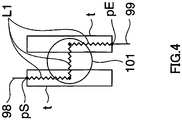
- strip members are employed in the switch of the comparative example shown in FIG. 4 as well, and that the external wiring patterns 98 and 99 are respectively connected to one end portion of each of the strip members t at the contact points pS and pE, which are power feed portions, as in the conventional example ( FIGS. 13A and 13B ).
- the length of the conductive path formed from the contact point pS to the contact point pE via the movable conductive portion 101 is L1.
- FIG. 5 is a schematic diagram of a specific example of the pair of fixed conductive portions 102 according to a first modified example.
- the strip members tA and tB are rectangular, and therefore an arrangement pitch P of the strip members tA and tB is the same at all positions in the extending direction, which is the direction orthogonal to the width direction (alignment direction) .
- the arrangement pitch P is defined as the distance between intermediate positions in the alignment direction. Note that letting D be the gap between the closest portions of the adjacent strip members tA and tB, the gap D is the same at all positions in the extending direction of the strip members tA and tB.
- the first main conductive pattern dA also extends under the strip members tA1 and tA2 on the substrate 93. Accordingly, practically, the first end portion tAlf and the second end portion tA1r have approximately the same potential, and the first end portion tA2f and the second end portion tA2r also have approximately the same potential.
- the second main conductive pattern dB also extends under the strip members tB1 and tB2. Accordingly, practically, the first end portion tB1f and the second end portion tB1r have approximately the same potential, and the first end portion tB2f and the second end portion tB2r also have approximately the same potential.
- the arrangement pitch of the central portion in the extending direction is smaller than that of the two end portions of the strip members t (on the first end portion tA2f and tB1f side, and on the second end portion tA2r and tB1r side) . Accordingly, even with a configuration in which the fixed conductive portions cA and cB each have two or more strip members t, the resistance value for the total length of the conductive path can be readily set smaller than in the configuration shown in FIG. 2 , and this is advantageous in improving the resistance characteristic.
- the strip members t need only be shaped as long and thin strips, are not required to have straight line portions, and may have an overall curved shape.
- the switch body 10 has one switch SW.
- two or more switches SW may be provided, and there are three switches SW in an exemplary configuration according to a second embodiment of the present invention.
- a movable conductive portion 101-1 and a pair of fixed conductive portions 102-1 constitute the switch SW1
- a movable conductive portion 101-2 and a pair of fixed conductive portions 102-2 constitute the switch SW2
- a movable conductive portion 101-3 and a pair of fixed conductive portions 102-3 constitute the switch SW3.
- FIG. 8B is a partial configuration diagram of a control circuit.
- the switches SW1, SW2, and SW3 are each connected to the external wiring pattern 98 via the first main conductive pattern dA. Also, the switches SW1, SW2, and SW3 are respectively connected to external wiring patterns 99-1, 99-2, and 99-3 via second main conductive patterns dB-1, dB-2, and dB-3.
- the second main conductive patterns dB-1, dB-2, and dB-3 are connected to the external wiring patterns 99-1, 99-2, and 99-3 through through-holes 81 (81-1, 81-2, 81-3) formed in the substrate 93. Two through-holes 81 are provided for each of the switches SW.
- Other configurations of the control circuit are the same as in the first embodiment.
- the first fixed conductive portions cA (cA-1, cA-2, cA-3) and the second fixed conductive portions cB (cB-1, cB-2, cB-3) constitute the fixed conductive portions 102-1, 102-2, and 102-3.
- the first fixed conductive portion cA-1 has strip members tA1, tA2, and tA3
- the second fixed conductive portion cB-1 has strip members tB1 and tB2. In this way, an odd number of strip members t constitute the first fixed conductive portion cA, and an even number of strip members t constitute the second fixed conductive portion cB.
- holes 83 are formed in the resist 70 in correspondence with the through-holes 81 (81-1, 81-2, 81-3).
- the resist 70 is also provided with multiple conduction holes h for putting the main conductive patterns dA and dB and the fixed conductive portions cA and cB, which are laminated on each other, into conduction with each other.
- conduction holes h1 to h8 are formed.
- conduction holes h2 and h6 are formed at positions corresponding to the first end portion tB1f and the second end portion tB1r of the strip member tB1.
- the strip members tA1 and tA3 have a short length, and therefore one corresponding conduction hole h is provided for each of them, and the conduction efficiency is raised by causing the region spanning the two end portions in the extending direction of the strip members tA1 and tA3 to come into contact with the first main conductive pattern dA, but conduction holes h may be provided at positions corresponding to the two end portions.
- a configuration is possible in which a conduction hole h is added at a position corresponding to an intermediate position in the extending direction, thus causing these strip members to come into contact with the main conductive patterns dA and dB at an intermediate position in the extending direction in addition to the two end portions.
- the configurations of the fixed conductive portions cA-2, cA-3, cB-2, and cB-3 and the corresponding conduction holes h are the same as the configurations of the fixed conductive portions cA-1 and cB-1 and the corresponding conduction holes h.
- the main conductive patterns dA and dB are formed so as to be somewhat larger than or the same size as the fixed conductive portions cA and cB, and therefore the fixed conductive portions cA and cB are formed in ranges that do not extend beyond the main conductive patterns dA and dB.
- the first fixed conductive portion cA is laminated on the first main conductive pattern dA, and, regarding the arrangement range of the strip members t in the extending direction, the arrangement range of the first main conductive pattern dA contains the arrangement range of the strip members t that constitute the first fixed conductive portion cA.
- the second fixed conductive portion cB is laminated on the second main conductive pattern dB, and, regarding the arrangement range of the strip members t in the extending direction, the arrangement range of the second main conductive pattern dB contains the arrangement range of the strip members t that constitute the second fixed conductive portion cB.
- the main conductive patterns dA and dB have shapes that are approximately the same as the strip members constituting the fixed conductive portions cA and cB, and that the arrangement ranges thereof approximately match each other. Due to the resist 70 being arranged between the fixed conductive portions cA and cB and the main conductive patterns dA and dB, as long as the conduction holes h1 to h8 do not extend beyond the patterns of the fixed conductive portions cA and cB, even if the main conductive patterns dA and dB extend beyond the patterns of the fixed conductive portions cA and cB, shorting will not occur in this circuit.
- the main conductive patterns dA and dB are configured such that the portions thereof having the strip members t that constitute the fixed conductive portions cA and cB laminated thereon are continuous without interruptions in the extending direction of the strip members t. If the main conductive patterns dA and dB were partially non-continuous, portions of the surfaces of the fixed conductive portions cA and cB that come into contact with the movable conductive portion 101 would be low regions, and the band-shaped contact region would be non-continuous. As the number of such regions increases, the contact area decreases in size, and the total resistance increases.
- the main conductive patterns dA and dB are configured such that at least the portions thereof having the strip members t laminated thereon are continuous without interruption in the extending direction of the strip members t.
- the strip members tA2 in the center in the alignment direction in the respective first fixed conductive portions cA-1, cA-2, and cA-3 are connected by the same first main conductive pattern dA.
- the end portion of the strip member tA2 of one of the sets is physically connected to the end portion of the strip member tA2 of the other adjacent set.
- All of the strip members tA1 and tA3 that constitute the first fixed conductive portions cA-1, cA-2, and cA-3 are in electrical conduction with each other via the first main conductive pattern dA.
- strip members tA1, tA2 and tA3 that constitute the first fixed conductive portions cA-1, cA-2, and cA-3 are required to be in electrical conduction with each other.
- a configuration is possible in which at least one of strip members tA1, tA2 and tA3 of the fixed conductive portion is in electrical conduction with the one of other fixed conductive portion, and is connected to the microcomputer.
- a configuration is possible in which the gap between adjacent strip members tA2 is set to a gap of 0 by design, and the strip members tA2 may be non-continuous or continuous with each other.
- FIG. 11B a configuration is possible in which adjacent strip members tA2 are continuous with each other, and consequently the three strip members tA2 are continuous with each other.
- this configuration becomes difficult to realize with comb teeth-shaped fixed conductive portions.
- FIG. 12 is a schematic diagram of fixed conductive portions configured as described in a comparative example.
- the strip members tA that constitute the first fixed conductive portion cA-1 and the strip members tB that constitute the second fixed conductive portion cB-1 are arranged in an alternating manner.
- the strip members tA that constitute the first fixed conductive portion cA-2 and the strip members tB that constitute the second fixed conductive portion cB-2 are arranged in an alternating manner, but the arrangement sequence is different from that of the first switch, such that they alternate.
- the strip members tA must not be in electrical conduction with the strip members tB, and therefore in order to reliably ensure gaps between adjacent end portions of the strip members tA and strip members tB, leeway needs to be provided in design, with consideration given to manufacturing tolerance as well. In comparison to the present embodiment, this is therefore a disadvantage in terms of the close arrangement of switches.
- At least the two end portions of the strip members tA and tB are connected to the main conductive patterns dA and dB, thus making it possible to achieve the same effects as the first embodiment in terms of improving the resistance characteristic of the conductive path during switching.
- the arrangement pitch of the strip members t is smaller in the central portion in the extending direction than in the two end portions, and therefore it is possible to achieve the same effects as the configurations shown in FIGS. 5 and 7 in terms of making it easier to shorten the conductive path.
- the fixed conductive portions cA and cB are formed in ranges that do not extend beyond the main conductive patterns dA and dB, and therefore the surfaces that come into contact with the movable conductive portion 101 are more readily made smooth, thus making it possible to raise the circuit reliability.
- the adjacent end portions of strip members tA2 are physically connected to each other.
- multiple sets (three sets in the present embodiment) of conductive portions, each set including the first fixed conductive portion cA, the second fixed conductive portion cB, and the movable conductive portion 101, are provided in correspondence with one operator (switch body 10), the sets of conductive portions are arranged along the extending direction of the strip members t, and the respective adjacent end portions of the central strip member tA2 that constitutes the first fixed conductive portion cA of one set and the central strip member tA that constitutes the first fixed conductive portion cA of an adjacent set are physically connected to each other.
- multiple sets of conductive portions are arranged along the extending direction of the strip member refers to a state in which the arrangement direction of the sets and the extending direction of the strip member match each other to the extent that the end portions of strip members arranged in the center of adjacent sets can be physically connected, and the arrangement direction and the extending direction of the strip members are orthogonal to each other.
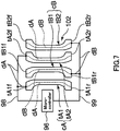
- the first fixed conductive portions cA (cA-1, cA-2, cA-3) each have three strip members tA (tAl, tA2, tA3)
- the second fixed conductive portions cB (cB-1, cB-2, cB-3) each have two strip members tB (tB1, tB2).
- the overall shape of the first and second fixed conductive portions is set to an elliptical shape.
- the key 92 and the substrate 93 of the electronic musical instrument according to the present embodiment have an elongated shape that is elongated in one direction, and their dimensional and positional precision are higher in the widthwise direction than in the lengthwise direction. For this reason, the probability distribution of positions of contact with the movable conductive portion has an elliptical shape.
- the conduction holes h1 and h5 may be made larger than the strip members tA1 and tA3 respectively.
- a configuration is possible in which that strip member tB or those strip members tB are in full-area contact with the second main conductive pattern dB.
- a configuration is possible in which in the strip members that constitute the first fixed conductive portion or the second fixed conductive portion and are located at the two ends in the alignment direction, the region spanning the two end portions in the extending direction comes into contact with the corresponding main conductive pattern. Accordingly, although the movable conductive portion 101 tends to unstably land on the strip members t at the two ends, the resistance value is lowered by causing the full area of the strip members t at the two ends to come into contact with the main conductive pattern, thus improving the resistance characteristic and making it possible to raise the operation detection precision.
Landscapes
- Engineering & Computer Science (AREA)
- Physics & Mathematics (AREA)
- Acoustics & Sound (AREA)
- Multimedia (AREA)
- Microelectronics & Electronic Packaging (AREA)
- Electrophonic Musical Instruments (AREA)
- Rotary Switch, Piano Key Switch, And Lever Switch (AREA)
- Contacts (AREA)
- Push-Button Switches (AREA)
Description
- The present invention relates to an operator device for an electronic musical instrument that detects an operation when an operator is operated so as to electrically short a pair of fixed conductive portions with a movable conductive portion.
- Conventionally, it is known that in an operator device for an electronic musical instrument such as a keyboard instrument, a pair of fixed conductive portions are mounted on a printed circuit board, and a movable conductive portion that can be moved by an operator is provided so as to oppose these fixed contact patterns. In this type of operator device, as illustrated in FIG. 14 and the like of
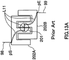
Patent Literature 1 noted below, the fixed conductive portions are widely known to be constituted by a pair of comb teeth-shaped contact patterns, and the movable conductive portion brings the pair of comb teeth-shaped fixed contact patterns into conduction, via itself, upon coming into contact with them. The fixed conductive portions and the movable conductive portion are generally constituted by carbon or the like.FIGS. 13A and13B are schematic diagrams showing contact between typical comb teeth-shaped fixed contact patterns and a circular movable conductive portion.
Patent literature 2 discloses an operator device for an electronic musical instrument according to the preamble part ofclaim 1. -
- Patent Literature 1:
JP H08-235952A - Patent Literature 2:
US 5,660,269 - As shown in
FIG. 13A ,external wiring patterns fixed contact patterns conductive portion 201 shorts a portion of the combs in thefixed contact patterns conductive portion 201. The length of this conductive path is L11. Also, in the example shown inFIG. 13B , the length of the conductive path from the contact point pS to the contact point pE is L12. - Here, a highly conductive material such as copper foil is used for the
external wiring patterns fixed contact patterns conductive portion 201 are made of carbon, which has a lower conductivity than copper foil. Carbon has a higher electric resistance than copper foil, and therefore the resistance characteristic degrades if the conductive path through carbon is too long. This has a negative influence on operation detection precision as well. A shorter conductive path during switching is more advantageous. In order to shorten the conductive path, it is desirable to give consideration not only to the distance from the power feed portion to the position of contact between the movableconductive portion 201 and the fixedcontact patterns conductive portion 201 as well. - One aspect of the present invention was achieved in order to solve the above-described problem in conventional technology, and an object of this aspect of the present invention is to provide an operator device for an electronic musical instrument that can improve the resistance characteristic of the conductive path during switching.
- In order to achieve the aforementioned object, an operator device for an electronic musical instrument as defined in
claim 1 is provided according to one aspect of the present invention. Advantageous embodiments can be configured according to any of claims 2-8. - According to the present invention, it is possible to improve the resistance characteristic of the conductive path during switching.
-
-
FIG. 1A is a schematic diagram of a portion of an electronic musical instrument to which an operator device according to a first embodiment is to be applied; -
FIG. 1B is a schematic diagram of the portion of the electronic musical instrument to which the operator device according to the first embodiment is to be applied; -
FIG. 1C is a partial configuration diagram of a control circuit in a single-throw switch; -
FIG. 2 is a schematic diagram of a specific example of a pair of fixed conductive portions; -
FIG. 3 is a schematic diagram of conductive paths in a switch configured as shown inFIG. 2 ; -
FIG. 4 is a schematic diagram of a conductive path in a switch configured as described in a comparative example; -
FIG. 5 is a schematic diagram of a specific example of a pair of fixed conductive portions according to a first modified example; -
FIG. 6 is a schematic diagram of conductive paths in a switch configured as described in the first modified example; -
FIG. 7 is a schematic diagram of a specific example of a pair of fixed conductive portions according to a second modified example; -
FIG. 8A is a schematic diagram of a switch body region of an electronic musical instrument to which an operator device according to a second embodiment is to be applied; -
FIG. 8B is a partial configuration diagram of a control circuit according to the second embodiment; -
FIG. 9A is a diagram showing a configuration of the fixed members that are arranged on a substrate in three sets of switches; -
FIG. 9B is a diagram showing first and second main conductive patterns; -
FIG. 10A is a diagram showing a resist; -
FIG. 10B is a diagram showing three sets of first and second fixed conductive portions; -
FIG. 10C is a cross-sectional diagram taken along line A-A inFIG. 9A ; -
FIG. 11A is a diagram showing a variation of three sets of first fixed conductive portions; -
FIG. 11B is a diagram showing a variation of three sets of second fixed conductive portions; -
FIG. 12 is a schematic diagram of fixed conductive portions configured as described in a comparative example; -
FIG. 13A is a schematic diagram showing contact between comb teeth-shaped fixed contact patterns and a circular movable conductive portion; and -
FIG. 13B is a schematic diagram showing contact between comb teeth-shaped fixed contact patterns and a circular movable conductive portion. - Hereinafter, embodiments of the present invention will be described with reference to the drawings.
-
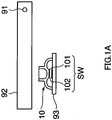
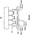
FIG. 1A is a schematic diagram showing a portion of an electronic musical instrument to which an operator device according to a first embodiment of the present invention is to be applied. A keyboard device of this electronic musical instrument hasmultiple keys 92 as playing operators. Asubstrate 93 is arranged under thekeys 92, and switchbodies 10 are arranged on thesubstrate 93. When one of thekeys 92 is operated by being pressed, it pivots about afulcrum 91 and drives one of theswitch bodies 10. - Note that the driving bodies (operators) that drive the
switch bodies 10 are not limited to being thekeys 92, and may be hammers instead. In one example, as shown inFIG. 1B , ahammer 95 is pivotably coupled to a key 92 by apivot shaft portion 94. Thehammer 95 is arranged so as to be capable of pivoting about afulcrum 89. Thesubstrate 93 is arranged above thehammer 95, and theswitch body 10 is arranged on the lower surface of thesubstrate 93. When the key 92 is operated by being pressed, thehammer 95 is driven via thepivot shaft portion 94, and thehammer 95 pivots about thefulcrum 89 and drives theswitch body 10. - Incidentally, the
switch bodies 10 each have a basic configuration in which one contact switch is constituted by a movable contact and fixed contacts. Theswitch body 10 has a movableconductive portion 101 that is configured to move by a driving body, and a pair of fixedconductive portions 102 that are arranged on thesubstrate 93, and these portions constitute one switch SW. The movableconductive portion 101 electrically shorts the pair of fixedconductive portions 102 upon coming into contact with both of them, thus performing switching. The switch SW is provided in correspondence with the driving body, and the same number of switches SW as the number ofkeys 92 are provided in this embodiment. Hereinafter, for the sake of convenience, the following description will take the example of a single-throw switch body 10 in which one switch corresponds to onekey 92. -
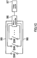
FIG. 1C is a partial configuration diagram of a control circuit in a single-throw switch. Switches SW are collectively organized into blocks for each key, the blocks are individually connected to amicrocontroller 96, and various types of music control are performed by performing time-division key scanning in units of blocks.External wiring patterns microcontroller 96. The movableconductive portion 101 puts theexternal wiring patterns microcontroller 96 includes a CPU and a storage unit, and is connected to ausage circuit 97. Theusage circuit 97 has a function for generating physical sounds and forming various types of musical sounds, and also has the musical sound production functionality of an amplifier, a speaker, or the like. -
FIG. 2 is a schematic diagram showing a specific example of the pair of fixedconductive portions 102 in the present embodiment. In this figure, the surface of thesubstrate 93 on the side having the fixedconductive portions 102 arranged thereon is viewed from the perpendicular direction. - The pair of fixed
conductive portions 102 includes a first fixed conductive portion cA and a second fixed conductive portion cB that make up a pair of electrodes. The fixed conductive portions cA and cB both do not have a comb teeth shape overall. Specifically, the fixed conductive portions cA and cB respectively have strip members tA and tB that are shaped as long and thin strips, and the strip members tA and tB (referred to as "strip members t" hereinafter when not distinguishing between them, and the same following for the reference signs of other constituent elements as well) are aligned in parallel with each other. A first main conductive pattern dA and a second main conductive pattern dB are arranged on thesubstrate 93 in correspondence with the first fixed conductive portion cA and the second fixed conductive portion cB respectively. Note that either or both of theexternal wiring patterns substrate 93. The main conductive patterns dA and dB are electrically connected to theexternal wiring patterns - Both a first end portion tAf and a second end portion tAr of the strip member tA in the extending direction (lengthwise direction) thereof are electrically connected to the first main conductive pattern dA. Both a first end portion tBf and a second end portion tBr of the strip member tB in the extending direction thereof are electrically connected to the second main conductive pattern dB.
- The movable
conductive portion 101 and the strip members t are constituted by a conductive material such as carbon. However, a conductive material other than carbon may be used, such as gold plating, pressure-sensitive ink, silver paste, or a conductive paste made up of a conductive filler and a binder such as epoxy resin. The main conductive patterns dA and dB are formed using a material that is sufficiently more conductive than the strip members t, such as a copper foil pattern. - In the switch SW, conductive paths are formed during switching due to the movable conductive portion electrically shorting the corresponding pair of fixed conductive portions upon coming into contact with both of them, and these conductive paths will be compared with a configuration according to a comparative example.
FIG. 3 is a schematic diagram of conductive paths in the switch SW of the present embodiment shown inFIG. 2 .FIG. 4 is a schematic diagram of a conductive path in a switch configured as described in a comparative example. - Assume that strip members are employed in the switch of the comparative example shown in
FIG. 4 as well, and that theexternal wiring patterns FIGS. 13A and13B ). The length of the conductive path formed from the contact point pS to the contact point pE via the movableconductive portion 101 is L1. - However, in the switch SW of the present embodiment (
FIG. 2 ), theexternal wiring patterns FIG. 3 , a conductive path from the contact point pS to the contact point pE is formed via the movableconductive portion 101 on the first end portion tAf and tBf side, and a conductive path from the contact point pS to the contact point pE is formed via the movableconductive portion 101 on the second end portion tAr and tBr side as well. The lengths of these two conductive paths are both L2. - The resistance value of a conductive path is proportional to the length thereof. Here, the material making up the movable
conductive portion 101 and the strip members t is carbon in both the conventional example and the present embodiment. A comparison of the lengths shows that L2 is less than or equal to L1, and a comparison of one conductive path in the comparative example and the present embodiment shows that the resistance value in the comparative example is greater than or equal to that in the present embodiment. Furthermore, in the present embodiment, two conductive paths with the length L2 are formed in parallel, and the value of the combined resistance in the present embodiment can be reliably set to a value smaller than, specifically 1/2 or less than, the resistance value in the comparative example. - For this reason, according to the present embodiment, it is possible to improve the resistance characteristic of the conductive path formed by the movable
conductive portion 101 and the fixedconductive portions 102 during switching. Accordingly, it is possible to raise the operation detection precision. - Next, modified examples of the first embodiment will be described with reference to
FIGS. 5 to 7 . -
FIG. 5 is a schematic diagram of a specific example of the pair of fixedconductive portions 102 according to a first modified example. In the configuration shown inFIG. 2 , the strip members tA and tB are rectangular, and therefore an arrangement pitch P of the strip members tA and tB is the same at all positions in the extending direction, which is the direction orthogonal to the width direction (alignment direction) . The arrangement pitch P is defined as the distance between intermediate positions in the alignment direction. Note that letting D be the gap between the closest portions of the adjacent strip members tA and tB, the gap D is the same at all positions in the extending direction of the strip members tA and tB. - In contrast, in the first modified example (
FIG. 5 ), the strip members tA and tB are not shaped as simple rectangles, and instead the first end portions tAf and tBf and the second end portions tAr and tBr deviate outward in the width direction relative to the central portions in the extending direction. An arrangement pitch P1 in the central portion in the extending direction of the strip members tA and tB is smaller than an arrangement pitch P2 in the two end portions of the strip members tA and tB. Also, the gap D in the central portion in the extending direction is smaller than the gap D in the two end portions. Note that the arrangement pitch P2 in the end portions is approximately the same value as the arrangement pitch P inFIG. 2 (P1<P2≈P). -
FIG. 6 is a schematic diagram of conductive paths in the switch SW of the first modified example shown inFIG. 5 . In this example, the positions of the contact points pS and pE are the same as in the example inFIG. 3 . However, the arrangement pitch P1 in the central portion in the extending direction is smaller, and therefore the conductive path in the movableconductive portion 101 is shorter. As a result, a length L3 of the conductive path formed from the contact point pS to the contact point pE via the movableconductive portion 101 is less than or equal to the length L2 (L3≤L2). Accordingly, the resistance value for the total length of the conductive path can be readily set smaller than in the configuration shown inFIG. 2 , and this is advantageous in improving the resistance characteristic. -
FIG. 7 is a schematic diagram of a specific example of the pair of fixedconductive portions 102 according to a second modified example. Multiple strip members tA (tAl, tA2) and tB (tB1, tB2) may constitute the fixed conductive portions cA and cB respectively. In this case, the strip members tA and the strip members tB are alternatingly arranged in parallel. In the exemplary configuration according to the second modified example (FIG. 7 ), two strip members tA and two strip members tB are provided. The strip members tA1, tB1, tA2, and tB2 are arranged side-by-side in the stated order. It should be noted that it is not easy to make a connection to the main conductive patterns dA and dB in the two end portions, and therefore the main conductive patterns dA and dB are arranged so as to also extend under the strip members tA and tB. - As shown in
FIG. 7 , the first main conductive pattern dA also extends under the strip members tA1 and tA2 on thesubstrate 93. Accordingly, practically, the first end portion tAlf and the second end portion tA1r have approximately the same potential, and the first end portion tA2f and the second end portion tA2r also have approximately the same potential. Similarly, the second main conductive pattern dB also extends under the strip members tB1 and tB2. Accordingly, practically, the first end portion tB1f and the second end portion tB1r have approximately the same potential, and the first end portion tB2f and the second end portion tB2r also have approximately the same potential. - In this example as well, similarly to the first modified example (
FIG. 5 ), the arrangement pitch of the central portion in the extending direction is smaller than that of the two end portions of the strip members t (on the first end portion tA2f and tB1f side, and on the second end portion tA2r and tB1r side) . Accordingly, even with a configuration in which the fixed conductive portions cA and cB each have two or more strip members t, the resistance value for the total length of the conductive path can be readily set smaller than in the configuration shown inFIG. 2 , and this is advantageous in improving the resistance characteristic. Note that the strip members t need only be shaped as long and thin strips, are not required to have straight line portions, and may have an overall curved shape. - In the configuration of the first embodiment, the
switch body 10 has one switch SW. However, two or more switches SW may be provided, and there are three switches SW in an exemplary configuration according to a second embodiment of the present invention. -
FIG. 8A is a schematic diagram of theswitch body 10 region of an electronic musical instrument to which an operator device according to the second embodiment is to be applied. The key 92 is used as the driving body, but the driving body may be thehammer 95. Theswitch body 10 is a triple-throw switch and has three sets of switches SW (SW1 to SW3), each of which includes a pair of fixedconductive portions 102 and one movableconductive portion 101. The switches SW1 to SW3 are arranged in a line in the lengthwise direction of the key 92. A movable conductive portion 101-1 and a pair of fixed conductive portions 102-1 constitute the switch SW1, a movable conductive portion 101-2 and a pair of fixed conductive portions 102-2 constitute the switch SW2, and a movable conductive portion 101-3 and a pair of fixed conductive portions 102-3 constitute the switch SW3. -
FIG. 8B is a partial configuration diagram of a control circuit. The switches SW1, SW2, and SW3 are each connected to theexternal wiring pattern 98 via the first main conductive pattern dA. Also, the switches SW1, SW2, and SW3 are respectively connected to external wiring patterns 99-1, 99-2, and 99-3 via second main conductive patterns dB-1, dB-2, and dB-3. The second main conductive patterns dB-1, dB-2, and dB-3 are connected to the external wiring patterns 99-1, 99-2, and 99-3 through through-holes 81 (81-1, 81-2, 81-3) formed in thesubstrate 93. Two through-holes 81 are provided for each of the switches SW. Other configurations of the control circuit are the same as in the first embodiment. -
FIG. 9A is a diagram showing a configuration of the fixed members that are arranged on thesubstrate 93 in the three sets of switches SW.FIG. 9B is a diagram showing the first main conductive pattern dA and the second main conductive patterns dB.FIG. 10A is a diagram showing a resist.FIG. 10B is a diagram showing three sets of first fixed conductive portions cA and three sets of second fixed conductive portions cB.FIG. 10C is a cross-sectional diagram taken along line A-A inFIG. 9A . - First, as partially shown in
FIG. 10C as well, the fixed members of the switches SW have a three-layer structure in which the main conductive patterns dA and dB are provided on the upper side of thesubstrate 93, a resist 70, which is an insulating material, is provided on the upper sides of the main conductive patterns dA and dB, and then the fixed conductive portions cA and cB are provided on the upper side of the resist 70. - As shown in
FIG. 10B , the first fixed conductive portions cA (cA-1, cA-2, cA-3) and the second fixed conductive portions cB (cB-1, cB-2, cB-3) constitute the fixed conductive portions 102-1, 102-2, and 102-3. The first fixed conductive portion cA-1 has strip members tA1, tA2, and tA3, and the second fixed conductive portion cB-1 has strip members tB1 and tB2. In this way, an odd number of strip members t constitute the first fixed conductive portion cA, and an even number of strip members t constitute the second fixed conductive portion cB. It should be noted that the numbers of strip members t that constitute the fixed conductive portions cA and cB are not limited to this example, and in the case where the fixed conductive portions cA and cB are constituted by multiple strip members t, the fixed conductive portions cA and cB may be constituted by either an even number or an odd number of strip members t. - As shown in
FIG. 9B , the first main conductive pattern dA is a common conductive portion that is common to the three first fixed conductive portions cA-1, cA-2, and cA-3, and is formed as a single body. On the other hand, in the case of the second main conductive pattern dB, the second main conductive patterns dB-1, dB-2, and dB-3 are formed so as to be physically separated from each other in correspondence with the three second fixed conductive portions cB-1, cB-2, and cB-3. The main conductive patterns dB-1, dB-2, and dB-3 are formed two each. Holes 82 (82-1, 82-2, 82-3) are formed in the main conductive patterns dB-1, dB-2, and dB-3 in correspondence with the through-holes 81 (81-1, 81-2, 81-3). - The following describes the fixed conductive portions cA-1 and cB-1 as representatives among the three fixed conductive portions cA and cB, with reference to
FIG. 10B . The strip members tA1, tB1, tA2, tB2, and tA3 are arranged side-by-side in the stated order. The arrangement direction of the strip members t (the left-right direction inFIG. 10B ) is approximately orthogonal to the extending direction of the strip members t (the up-down direction inFIG. 10B ). Also, the switches SW1 to SW3 are arranged along the extending direction of the strip members t. Accordingly, the alignment direction of the strip members t is approximately orthogonal to the arrangement direction of the switches SW1 to SW3 (lengthwise direction of the key 92) . The strip member tA2 that constitutes the first fixed conductive portion cA-1 is located in the center in the alignment direction among the five strip members t, and the length of the strip member tA2 is the longest among the five strip members t. Also, the lengths of the five strip members t are shorter the farther the strip members t are from the center in the alignment direction. Accordingly, the overall shape formed by the five strip members t is an ellipse that is elongated in the alignment direction. Considering the operation of the key 92 and thehammer 95, the region of the fixedconductive portions 102 that is envisioned to come into contact with the movableconductive portion 101 in the direction orthogonal to the alignment direction of the strip members t is thought to be shorter the farther the position is from the center in the alignment direction. For this reason, even if the strip members t far from the center in the alignment direction are formed with a long length, portions that do not come into contact with the movableconductive portion 101 would merely increase in size, and this would not have much meaning. In view of this, the lengths satisfy the relationship tA1=tA3<tB1=tB2<tA2. Accordingly, it is possible to reduce the amount of needless space for arrangement of the strip members t. - Also, the configurations shown in
FIGS. 5 and7 are employed for the arrangement pitch of the strip members t. In other words, the arrangement pitch in the central portion in the extending direction is smaller than the arrangement pitch in the two end portions of the strip members t. Regarding the gap as well, the gap is smaller in the central portion in the extending direction than in the two end portions of the strip members t. - As shown in
FIG. 10A , holes 83 (83-1, 83-2, 83-3) are formed in the resist 70 in correspondence with the through-holes 81 (81-1, 81-2, 81-3). The resist 70 is also provided with multiple conduction holes h for putting the main conductive patterns dA and dB and the fixed conductive portions cA and cB, which are laminated on each other, into conduction with each other. In the case of the configuration corresponding to the fixed conductive portions cA-1 and cB-1, conduction holes h1 to h8 are formed. Specifically, conduction holes h2 and h6 are formed at positions corresponding to the first end portion tB1f and the second end portion tB1r of the strip member tB1. Conduction holes h3 and h7 are formed at positions corresponding to the first end portion tA2f and the second end portion tA2r of the strip member tA2. Conduction holes h4 and h8 are formed at positions corresponding to the first end portion tB2f and the second end portion tB2r of the strip member tB2. A conduction hole h1 is formed in correspondence with the strip member tA1. A conduction hole h5 is formed in correspondence with the strip member tA3. - As can be understood from
FIGS. 9B ,10A , and10B , the strip members tA1, tA2, and tA3 come into contact with and into electrical conduction with the first main conductive pattern dA through the conduction holes h1, h3, h7, and h5. The strip members tB1 and tB2 come into contact with and into electrical conduction with the second main conductive patterns dB through the conduction holes h2, h4, h6, and h8. In particular, in the case of the strip member tA2, the two end portions thereof (tA2f, tA2r) come into contact with the first main conductive pattern dA, and therefore the two end portions practically have approximately the same potential. In the case of the strip members tB1 and tB2 as well, the two end portions thereof (tB1f, tB1r, tB2f, tB2r) come into contact with the second main conductive patterns dB, and therefore the two end portions practically have approximately the same potential. - Note that the strip members tA1 and tA3 have a short length, and therefore one corresponding conduction hole h is provided for each of them, and the conduction efficiency is raised by causing the region spanning the two end portions in the extending direction of the strip members tA1 and tA3 to come into contact with the first main conductive pattern dA, but conduction holes h may be provided at positions corresponding to the two end portions. Also, in the case of the strip members tA2, tB1, and tB2, a configuration is possible in which a conduction hole h is added at a position corresponding to an intermediate position in the extending direction, thus causing these strip members to come into contact with the main conductive patterns dA and dB at an intermediate position in the extending direction in addition to the two end portions. The configurations of the fixed conductive portions cA-2, cA-3, cB-2, and cB-3 and the corresponding conduction holes h are the same as the configurations of the fixed conductive portions cA-1 and cB-1 and the corresponding conduction holes h.
- Note that the relationship between the arrangement ranges of the fixed conductive portions cA and cB and the main conductive patterns dA and dB is as follows. As partially illustrated in
FIG. 10C , the fixed conductive portions cA and cB are arranged on the upper sides of the main conductive patterns dA and dB, in ranges contained within the main conductive patterns dA and dB. Specifically, the fixed conductive portions cA and cB are arranged in ranges that are smaller than or the same size as the ranges of the main conductive patterns dA and dB. In other words, the main conductive patterns dA and dB are formed so as to be somewhat larger than or the same size as the fixed conductive portions cA and cB, and therefore the fixed conductive portions cA and cB are formed in ranges that do not extend beyond the main conductive patterns dA and dB. Accordingly, in the present embodiment, the first fixed conductive portion cA is laminated on the first main conductive pattern dA, and, regarding the arrangement range of the strip members t in the extending direction, the arrangement range of the first main conductive pattern dA contains the arrangement range of the strip members t that constitute the first fixed conductive portion cA. Similarly, the second fixed conductive portion cB is laminated on the second main conductive pattern dB, and, regarding the arrangement range of the strip members t in the extending direction, the arrangement range of the second main conductive pattern dB contains the arrangement range of the strip members t that constitute the second fixed conductive portion cB. - The formation precision and positional precision of the fixed conductive portions cA and cB made of carbon or the like are lower than those of the main conductive patterns dA and dB made of copper foil or the like. For this reason, in order to avoid the risk of shorting, the fixed conductive portions cA and cB generally need to be separated farther from each other than the main conductive patterns dA and dB. In contrast, in the present embodiment, the fixed conductive portions cA and cB are formed in ranges that do not extend beyond the main conductive patterns dA and dB, as described above. Accordingly, the fixed conductive portions cA and cB are reliably formed on the main conductive patterns dA and dB, and the surfaces of the fixed conductive portions cA and cB and that come into contact with the movable
conductive portion 101 are more readily made smooth. Also, the movableconductive portion 101 can be caused to come into contact with flat portions of the fixed conductive portions cA and cB, thus making it possible to raise the circuit reliability. - Note that from the viewpoints of cost reduction and compactness, regarding the arrangement range of the strip members t in the extending direction, it is preferable that the fixed conductive portions cA and cB geometrically match (are congruent with) the main conductive patterns dA and dB, and are exactly overlaid on each other without misalignment. However, in terms of the arrangement ranges, there may be slight differences between the two in at least one out of the shapes, positions, and sizes thereof, to the extent that there is no risk of shorting between patterns that do not have the same potential. In other words, the main conductive patterns dA and dB need only have shapes that conform to the strip members constituting the fixed conductive portions cA and cB. In other words, it is sufficient that the main conductive patterns dA and dB have shapes that are approximately the same as the strip members constituting the fixed conductive portions cA and cB, and that the arrangement ranges thereof approximately match each other. Due to the resist 70 being arranged between the fixed conductive portions cA and cB and the main conductive patterns dA and dB, as long as the conduction holes h1 to h8 do not extend beyond the patterns of the fixed conductive portions cA and cB, even if the main conductive patterns dA and dB extend beyond the patterns of the fixed conductive portions cA and cB, shorting will not occur in this circuit.
- Also, in the present embodiment, as illustrated in
FIG. 10B , the main conductive patterns dA and dB are configured such that the portions thereof having the strip members t that constitute the fixed conductive portions cA and cB laminated thereon are continuous without interruptions in the extending direction of the strip members t. If the main conductive patterns dA and dB were partially non-continuous, portions of the surfaces of the fixed conductive portions cA and cB that come into contact with the movableconductive portion 101 would be low regions, and the band-shaped contact region would be non-continuous. As the number of such regions increases, the contact area decreases in size, and the total resistance increases. The height of high positions on the contact surfaces also become unstable, and therefore the size of the contact area becomes unstable overall, and consequently the total resistance value also becomes unstable. Accordingly, in order to avoid this, it is preferable that the main conductive patterns dA and dB are configured such that at least the portions thereof having the strip members t laminated thereon are continuous without interruption in the extending direction of the strip members t. - As shown in
FIG. 10B , the strip members tA2 in the center in the alignment direction in the respective first fixed conductive portions cA-1, cA-2, and cA-3 are connected by the same first main conductive pattern dA. In other words, regarding the relationship between two sets that are adjacent to each other, the end portion of the strip member tA2 of one of the sets is physically connected to the end portion of the strip member tA2 of the other adjacent set. All of the strip members tA1 and tA3 that constitute the first fixed conductive portions cA-1, cA-2, and cA-3 are in electrical conduction with each other via the first main conductive pattern dA. Note that not all of the strip members tA1, tA2 and tA3 that constitute the first fixed conductive portions cA-1, cA-2, and cA-3 are required to be in electrical conduction with each other. A configuration is possible in which at least one of strip members tA1, tA2 and tA3 of the fixed conductive portion is in electrical conduction with the one of other fixed conductive portion, and is connected to the microcomputer. - Here, the adjacent end portions of the strip members tA2 in the center in the alignment direction are closer to each other than the adjacent end portions of the other strip members t. Normally, when compactly arranging the switches SW in a line, it is necessary to make the gap between the closest strip members t as short as possible, while also reliably ensuring the gap. However, in the configuration of the present embodiment, the three strip members tA2 may have the same potential, and therefore the gap between adjacent strip members tA2 can be easily set to a short gap. Alternatively, adjacent strip members tA2 may be formed so as to be continuous with each other. For example, as illustrated in
FIG. 11A , a configuration is possible in which the gap between adjacent strip members tA2 is set to a gap of 0 by design, and the strip members tA2 may be non-continuous or continuous with each other. Alternatively, as illustrated inFIG. 11B , a configuration is possible in which adjacent strip members tA2 are continuous with each other, and consequently the three strip members tA2 are continuous with each other. In the case where there are three or more sets of switches SW, this configuration becomes difficult to realize with comb teeth-shaped fixed conductive portions. In the present embodiment, it is easy to arrange multiple switches SW close to each other. - The following is a comparison given with reference to
FIG. 12. FIG. 12 is a schematic diagram of fixed conductive portions configured as described in a comparative example. In the first switch, the strip members tA that constitute the first fixed conductive portion cA-1 and the strip members tB that constitute the second fixed conductive portion cB-1 are arranged in an alternating manner. In the second switch, the strip members tA that constitute the first fixed conductive portion cA-2 and the strip members tB that constitute the second fixed conductive portion cB-2 are arranged in an alternating manner, but the arrangement sequence is different from that of the first switch, such that they alternate. The strip members tA must not be in electrical conduction with the strip members tB, and therefore in order to reliably ensure gaps between adjacent end portions of the strip members tA and strip members tB, leeway needs to be provided in design, with consideration given to manufacturing tolerance as well. In comparison to the present embodiment, this is therefore a disadvantage in terms of the close arrangement of switches. - Note that from the viewpoint of achieving an advantage in terms of the close arrangement of switches, such a configuration may be applied to the relationship between specific strip members t other than the strip members tA2. A configuration is possible in which adjacent end portions of specific strip members t are electrically connected to each other such that the specific strip members t in all of the switches SW are in electrical conduction with each other.
- According to the present embodiment, at least the two end portions of the strip members tA and tB are connected to the main conductive patterns dA and dB, thus making it possible to achieve the same effects as the first embodiment in terms of improving the resistance characteristic of the conductive path during switching.
- Also, the arrangement pitch of the strip members t is smaller in the central portion in the extending direction than in the two end portions, and therefore it is possible to achieve the same effects as the configurations shown in
FIGS. 5 and7 in terms of making it easier to shorten the conductive path. - Also, according to the present embodiment, the fixed conductive portions cA and cB are formed in ranges that do not extend beyond the main conductive patterns dA and dB, and therefore the surfaces that come into contact with the movable
conductive portion 101 are more readily made smooth, thus making it possible to raise the circuit reliability. - Also, in the present embodiment, in the relationship between switches SW that are adjacent to each other, the adjacent end portions of strip members tA2 are physically connected to each other. Specifically, multiple sets (three sets in the present embodiment) of conductive portions, each set including the first fixed conductive portion cA, the second fixed conductive portion cB, and the movable
conductive portion 101, are provided in correspondence with one operator (switch body 10), the sets of conductive portions are arranged along the extending direction of the strip members t, and the respective adjacent end portions of the central strip member tA2 that constitutes the first fixed conductive portion cA of one set and the central strip member tA that constitutes the first fixed conductive portion cA of an adjacent set are physically connected to each other. Accordingly, it is easy to arrange multiple switches SW close to each other, thus making it possible to increase the degree of freedom in design, and also reduce cost. Note that the phrase "multiple sets of conductive portions are arranged along the extending direction of the strip member" refers to a state in which the arrangement direction of the sets and the extending direction of the strip member match each other to the extent that the end portions of strip members arranged in the center of adjacent sets can be physically connected, and the arrangement direction and the extending direction of the strip members are orthogonal to each other. - Also, in the present embodiment, the first fixed conductive portions cA (cA-1, cA-2, cA-3) each have three strip members tA (tAl, tA2, tA3), and the second fixed conductive portions cB (cB-1, cB-2, cB-3) each have two strip members tB (tB1, tB2). In this way, an odd number of strip members constitute the first fixed conductive portions, and an even number of strip members constitute the second fixed conductive portions, thus making it possible for the total number of strip members constituting the first and second fixed conductive portions to be an odd number, and making it possible for one of the strip members of the first fixed conductive portion to be arranged in the center overall. Accordingly, by setting a long length for the central strip member, and setting a shorter length for the strip members the closer they are to the two sides, it is possible to set the overall shape of the first and second fixed conductive portions to an elliptical shape. The key 92 and the
substrate 93 of the electronic musical instrument according to the present embodiment have an elongated shape that is elongated in one direction, and their dimensional and positional precision are higher in the widthwise direction than in the lengthwise direction. For this reason, the probability distribution of positions of contact with the movable conductive portion has an elliptical shape. Accordingly, by setting the overall shape of the first and second fixed conductive portions to an elliptical shape, it is possible to cause the first and second fixed conductive portions and the movable conductive portion to efficiently come into contact with each other in the present embodiment. Also, in the case of providing multiple switches SW, as illustrated inFIGS. 11A and11B , if the strip members tA2 arranged in the center of the first fixed conductive portions are physically connected to each other so as to have the same potential, shorting can occur between the switches SW, thus making it easy to arrange the switches SW close to each other. - Also, the lengths of the strip members t that constitute the fixed conductive portions cA and cB are shorter the farther the strip members t are from the center in the alignment direction, and therefore it is possible to reduce the amount of needless space for arrangement of the strip members t, while also giving consideration to the envisioned region of contact with the movable
conductive portion 101. - Note that at the least, a configuration is possible in which merely the strip members t at the two ends (tAl, tA3) that are farthest from the center in the alignment direction come into full-area contact with the first main conductive pattern dA. In this case, for example, the conduction holes h1 and h5 may be made larger than the strip members tA1 and tA3 respectively. Similarly, even in the case where either or both of the strip members t at the two ends are strip members tB, a configuration is possible in which that strip member tB or those strip members tB are in full-area contact with the second main conductive pattern dB. In other words, a configuration is possible in which in the strip members that constitute the first fixed conductive portion or the second fixed conductive portion and are located at the two ends in the alignment direction, the region spanning the two end portions in the extending direction comes into contact with the corresponding main conductive pattern. Accordingly, although the movable
conductive portion 101 tends to unstably land on the strip members t at the two ends, the resistance value is lowered by causing the full area of the strip members t at the two ends to come into contact with the main conductive pattern, thus improving the resistance characteristic and making it possible to raise the operation detection precision. - Note that the present invention is also applicable to an operator other than a playing operator, and furthermore is also applicable to an electronic musical instrument other than a keyboard instrument.
- Although the present invention has been described in detail above based on preferred embodiments, the present invention is not limited to these specific embodiments, and the present invention encompasses various modes that do not depart from the scope of the appended claims. Portions of the embodiments described above may be combined as appropriate.
Claims (8)
- An operator device for an electronic musical instrument, the operator device comprising:a substrate;a first fixed conductive portion (cA) and a second fixed conductive portion (cB) that are arranged on the substrate (93) and make up a pair of electrodes;a first main conductive pattern (dA) and a second main conductive pattern (dB) that are arranged on the substrate (93), have a higher conductivity than the first and second fixed conductive portions (cA, cB), and respectively correspond to the first fixed conductive portion (cA) and the second fixed conductive portion (cB); anda movable conductive portion (101) that is configured to move by an operation performed on the operator, and electrically shorts the first fixed conductive portion (cA) and the second fixed conductive portion (cB) upon coming into contact with both of them,wherein the first fixed conductive portion (cA) and the second fixed conductive portion (cB) are each constituted by at least one strip member (tA, tB), and the strip member (tA) constituting the first fixed conductive portion (cA) and the strip member (tB) constituting the second fixed conductive portion (cB) are aligned in parallel and in an alternating manner, andat least two end portions (tAf, tAr) of the strip member (tA) constituting the first fixed conductive portion (cA) are electrically connected to the first main conductive pattern (dA), and at least two end portions (tBf, tBr) of the strip member (tB) constituting the second fixed conductive portion (cB) are electrically connected to the second main conductive pattern (dB),characterized in that
in the strip members (ta, tB) that constitute the first fixed conductive portion (cA) and the second fixed conductive portion (cB), an arrangement pitch in an alignment direction of the strip members (tA, tB) is smaller in a central portion in an extending direction of the strip members (tA, tB) than in the two end portions (tAf, tAr, tBf, tBr) of the strip members (tA, tB). - The operator device for an electronic musical instrument according to claim 1,
wherein the first fixed conductive portion (cA) is arranged on an upper side of the first main conductive pattern (dA) in a range the same as a range of the first main conductive pattern (dA), or is arranged on the upper side of the first main conductive pattern (dA) in a range that is contained within the range of the first main conductive pattern (dA) and is smaller than the range of the first main conductive pattern (dA), and
the second fixed conductive portion (cB) is arranged on an upper side of the second main conductive pattern (dB) in a range the same as a range of the second main conductive pattern (dB), or is arranged on the upper side of the second main conductive pattern (dB) in a range that is contained within the range of the second main conductive pattern (dB) and is smaller than the range of the second main conductive pattern (dB). - The operator device for an electronic musical instrument according to claim 1,
wherein the first fixed conductive portion (cA) is laminated on the first main conductive pattern (dA),
an arrangement range of the first main conductive pattern (dA) in the extending direction of the strip members (tA, tB) contains an arrangement range in the extending direction of the strip member (tA) constituting the first fixed conductive portion (cA),
a portion of the first main conductive pattern (dA) having the strip member (tA) constituting the first fixed conductive portion (cA) laminated thereon is continuous without interruption in the extending direction of the strip member (tA),
the second fixed conductive portion (cB) is laminated on the second main conductive pattern (dB),
an arrangement range of the second main conductive pattern (dB) in the extending direction of the strip members (tA, tB) contains an arrangement range in the extending direction of the strip member (tB) constituting the second fixed conductive portion (cB), and
a portion of the second main conductive pattern (dB) having the strip member (tB) constituting the second fixed conductive portion (cB) laminated thereon is continuous without interruption in the extending direction of the strip member (tB). - The operator device for an electronic musical instrument according to any one of the preceding claims,
wherein a plurality of sets of conductive portions, each set including the first fixed conductive portion (cA), the second fixed conductive portion (cB), and the movable conductive portion (101), are provided in correspondence with an operator,
the plurality of sets are arranged along the extending direction of the strip members (tA, tB) constituting the first fixed conductive portions (cA) and the second fixed conductive portions (cB) of the sets, and
respective adjacent end portions of the strip member (tA) constituting the first fixed conductive portion (cA) of one set and the strip member (tB) constituting the first fixed conductive portion (cB) of an adjacent set are physically connected to each other. - The operator device for an electronic musical instrument according to claim 4, wherein the number of sets is three or more.
- The operator device for an electronic musical instrument according to any one of the preceding claims, wherein an odd number of strip members (tAl, tA2, tA3) constitutes the first fixed conductive portion (cA), and an even number of strip members (tB1, tB2)) constitute the second fixed conductive portion (cB).
- The operator device for an electronic musical instrument according to any one of the preceding claims, wherein the length of each strip member (tA) constituting the first fixed conductive portion (cA) and each strip member (tB) constituting the second fixed conductive portion (cB) is shorter the farther the strip member (tA, tB) is from a center in an alignment direction of the strip members (tA, tB).
- The operator device for an electronic musical instrument according to any one of the preceding claims, wherein in strip members (tA, tB)) that constitute the first fixed conductive portion (cA) or the second fixed conductive portion (cB) and are located at two ends in the alignment direction, a region spanning two end portions in the extending direction comes into contact with the corresponding main conductive pattern (dA, dB).
Applications Claiming Priority (1)
| Application Number | Priority Date | Filing Date | Title |
|---|---|---|---|
| JP2015193263 | 2015-09-30 |
Publications (2)
| Publication Number | Publication Date |
|---|---|
| EP3151237A1 EP3151237A1 (en) | 2017-04-05 |
| EP3151237B1 true EP3151237B1 (en) | 2018-06-27 |
Family
ID=57047027
Family Applications (1)
| Application Number | Title | Priority Date | Filing Date |
|---|---|---|---|
| EP16191061.7A Active EP3151237B1 (en) | 2015-09-30 | 2016-09-28 | Operation device for electronic musical instrument |
Country Status (4)
| Country | Link |
|---|---|
| US (1) | US9767779B2 (en) |
| EP (1) | EP3151237B1 (en) |
| JP (1) | JP6724698B2 (en) |
| CN (1) | CN107045952B (en) |
Families Citing this family (1)
| Publication number | Priority date | Publication date | Assignee | Title |
|---|---|---|---|---|
| CN107045952B (en) * | 2015-09-30 | 2019-07-19 | 雅马哈株式会社 | Operator device for electronic musical instrument |
Family Cites Families (9)
| Publication number | Priority date | Publication date | Assignee | Title |
|---|---|---|---|---|
| DE3041859A1 (en) * | 1980-11-06 | 1982-06-03 | Preh Elektro Feinmechanik | KEYBOARD |
| US4580478A (en) * | 1984-02-06 | 1986-04-08 | Bitronics, Inc. | Musical keyboard using planar coil arrays |
| CN2038653U (en) * | 1988-07-28 | 1989-05-31 | 高建和 | Musical instrument in the form of a blanket |
| JPH07181970A (en) | 1993-12-24 | 1995-07-21 | Roland Corp | Sound effect addition device |
| JP3000885B2 (en) | 1994-12-28 | 2000-01-17 | ヤマハ株式会社 | Switch device |
| JP2904734B2 (en) * | 1995-11-15 | 1999-06-14 | ユニデン株式会社 | switch |
| JP2004022411A (en) * | 2002-06-18 | 2004-01-22 | Mitsumi Electric Co Ltd | Contact mechanism |
| JP2010282888A (en) * | 2009-06-05 | 2010-12-16 | Panasonic Electric Works Co Ltd | Contact device and relay device using the same |
| CN107045952B (en) * | 2015-09-30 | 2019-07-19 | 雅马哈株式会社 | Operator device for electronic musical instrument |
-
2016
- 2016-09-23 CN CN201610848920.8A patent/CN107045952B/en active Active
- 2016-09-28 EP EP16191061.7A patent/EP3151237B1/en active Active
- 2016-09-30 US US15/282,797 patent/US9767779B2/en active Active
- 2016-09-30 JP JP2016193160A patent/JP6724698B2/en active Active
Non-Patent Citations (1)
| Title |
|---|
| None * |
Also Published As
| Publication number | Publication date |
|---|---|
| US9767779B2 (en) | 2017-09-19 |
| US20170092250A1 (en) | 2017-03-30 |
| JP6724698B2 (en) | 2020-07-15 |
| JP2017068265A (en) | 2017-04-06 |
| EP3151237A1 (en) | 2017-04-05 |
| CN107045952B (en) | 2019-07-19 |
| CN107045952A (en) | 2017-08-15 |
Similar Documents
| Publication | Publication Date | Title |
|---|---|---|
| CN101820725B (en) | Flexible printed board | |
| JP6249991B2 (en) | Wiring module | |
| US7172446B1 (en) | Electrical connector | |
| US20100096165A1 (en) | Golden finger for flexible printed circuitboard | |
| JP5818516B2 (en) | Flexible printed circuit board having connector connection | |
| JP4551776B2 (en) | Double-sided FPC | |
| JP2014010966A (en) | Housingless connector | |
| EP3151237B1 (en) | Operation device for electronic musical instrument | |
| KR20160048172A (en) | Printed wiring board and connector connected to said wiring board | |
| US7731506B2 (en) | Pin layout of a golden finger for flexible printed circuitboard | |
| EP3483912B1 (en) | Electrically conductive loop of circuit breaker | |
| KR101516297B1 (en) | Tact switch for electronic component | |
| JP5169308B2 (en) | Printed circuit board and electronic device | |
| CN101925254B (en) | Flexible printing substrate and computer using flexible printing substrate | |
| JP2005316037A (en) | Display device | |
| JP2000112625A (en) | Structure for fitting light emitting element mounted on keyboard | |
| JP4672925B2 (en) | Flexible wiring board connector | |
| JP6942656B2 (en) | Printed wiring board | |
| US9378905B2 (en) | Inter-pole drive bar usable with switch apparatus having multiple poles | |
| US6169255B1 (en) | Flexible membrane circuit structure for keyswitch | |
| TW200514304A (en) | Structure for forming discharging path of a flexible printed circuit board | |
| CN110012594A (en) | A kind of flexible circuit board and terminal device | |
| CN220528277U (en) | Flexible circuit board and terminal equipment | |
| CN103915277A (en) | Regulation member and switch unit | |
| US20050162037A1 (en) | Film like electrode member for electrostatic motor |
Legal Events
| Date | Code | Title | Description |
|---|---|---|---|
| PUAI | Public reference made under article 153(3) epc to a published international application that has entered the european phase |
Free format text: ORIGINAL CODE: 0009012 |
|
| AK | Designated contracting states |
Kind code of ref document: A1 Designated state(s): AL AT BE BG CH CY CZ DE DK EE ES FI FR GB GR HR HU IE IS IT LI LT LU LV MC MK MT NL NO PL PT RO RS SE SI SK SM TR |
|
| AX | Request for extension of the european patent |
Extension state: BA ME |
|
| 17P | Request for examination filed |
Effective date: 20170830 |
|
| RBV | Designated contracting states (corrected) |
Designated state(s): AL AT BE BG CH CY CZ DE DK EE ES FI FR GB GR HR HU IE IS IT LI LT LU LV MC MK MT NL NO PL PT RO RS SE SI SK SM TR |
|
| GRAP | Despatch of communication of intention to grant a patent |
Free format text: ORIGINAL CODE: EPIDOSNIGR1 |
|
| RIC1 | Information provided on ipc code assigned before grant |
Ipc: H01H 13/702 20060101ALI20171219BHEP Ipc: G10H 1/055 20060101AFI20171219BHEP |
|
| INTG | Intention to grant announced |
Effective date: 20180116 |
|
| RAP1 | Party data changed (applicant data changed or rights of an application transferred) |
Owner name: YAMAHA CORPORATION |
|
| GRAS | Grant fee paid |
Free format text: ORIGINAL CODE: EPIDOSNIGR3 |
|
| GRAA | (expected) grant |
Free format text: ORIGINAL CODE: 0009210 |
|
| AK | Designated contracting states |
Kind code of ref document: B1 Designated state(s): AL AT BE BG CH CY CZ DE DK EE ES FI FR GB GR HR HU IE IS IT LI LT LU LV MC MK MT NL NO PL PT RO RS SE SI SK SM TR |
|
| REG | Reference to a national code |
Ref country code: GB Ref legal event code: FG4D |
|
| REG | Reference to a national code |
Ref country code: AT Ref legal event code: REF Ref document number: 1012999 Country of ref document: AT Kind code of ref document: T Effective date: 20180715 |
|
| REG | Reference to a national code |
Ref country code: IE Ref legal event code: FG4D |
|
| REG | Reference to a national code |
Ref country code: DE Ref legal event code: R096 Ref document number: 602016003814 Country of ref document: DE |
|
| PG25 | Lapsed in a contracting state [announced via postgrant information from national office to epo] |
Ref country code: LT Free format text: LAPSE BECAUSE OF FAILURE TO SUBMIT A TRANSLATION OF THE DESCRIPTION OR TO PAY THE FEE WITHIN THE PRESCRIBED TIME-LIMIT Effective date: 20180627 Ref country code: BG Free format text: LAPSE BECAUSE OF FAILURE TO SUBMIT A TRANSLATION OF THE DESCRIPTION OR TO PAY THE FEE WITHIN THE PRESCRIBED TIME-LIMIT Effective date: 20180927 Ref country code: FI Free format text: LAPSE BECAUSE OF FAILURE TO SUBMIT A TRANSLATION OF THE DESCRIPTION OR TO PAY THE FEE WITHIN THE PRESCRIBED TIME-LIMIT Effective date: 20180627 Ref country code: NO Free format text: LAPSE BECAUSE OF FAILURE TO SUBMIT A TRANSLATION OF THE DESCRIPTION OR TO PAY THE FEE WITHIN THE PRESCRIBED TIME-LIMIT Effective date: 20180927 Ref country code: SE Free format text: LAPSE BECAUSE OF FAILURE TO SUBMIT A TRANSLATION OF THE DESCRIPTION OR TO PAY THE FEE WITHIN THE PRESCRIBED TIME-LIMIT Effective date: 20180627 |
|
| REG | Reference to a national code |
Ref country code: NL Ref legal event code: MP Effective date: 20180627 |
|
| REG | Reference to a national code |
Ref country code: LT Ref legal event code: MG4D |
|
| PG25 | Lapsed in a contracting state [announced via postgrant information from national office to epo] |
Ref country code: GR Free format text: LAPSE BECAUSE OF FAILURE TO SUBMIT A TRANSLATION OF THE DESCRIPTION OR TO PAY THE FEE WITHIN THE PRESCRIBED TIME-LIMIT Effective date: 20180928 Ref country code: HR Free format text: LAPSE BECAUSE OF FAILURE TO SUBMIT A TRANSLATION OF THE DESCRIPTION OR TO PAY THE FEE WITHIN THE PRESCRIBED TIME-LIMIT Effective date: 20180627 Ref country code: LV Free format text: LAPSE BECAUSE OF FAILURE TO SUBMIT A TRANSLATION OF THE DESCRIPTION OR TO PAY THE FEE WITHIN THE PRESCRIBED TIME-LIMIT Effective date: 20180627 Ref country code: RS Free format text: LAPSE BECAUSE OF FAILURE TO SUBMIT A TRANSLATION OF THE DESCRIPTION OR TO PAY THE FEE WITHIN THE PRESCRIBED TIME-LIMIT Effective date: 20180627 |
|
| REG | Reference to a national code |
Ref country code: AT Ref legal event code: MK05 Ref document number: 1012999 Country of ref document: AT Kind code of ref document: T Effective date: 20180627 |
|
| PG25 | Lapsed in a contracting state [announced via postgrant information from national office to epo] |
Ref country code: NL Free format text: LAPSE BECAUSE OF FAILURE TO SUBMIT A TRANSLATION OF THE DESCRIPTION OR TO PAY THE FEE WITHIN THE PRESCRIBED TIME-LIMIT Effective date: 20180627 |
|
| PG25 | Lapsed in a contracting state [announced via postgrant information from national office to epo] |
Ref country code: PL Free format text: LAPSE BECAUSE OF FAILURE TO SUBMIT A TRANSLATION OF THE DESCRIPTION OR TO PAY THE FEE WITHIN THE PRESCRIBED TIME-LIMIT Effective date: 20180627 Ref country code: RO Free format text: LAPSE BECAUSE OF FAILURE TO SUBMIT A TRANSLATION OF THE DESCRIPTION OR TO PAY THE FEE WITHIN THE PRESCRIBED TIME-LIMIT Effective date: 20180627 Ref country code: SK Free format text: LAPSE BECAUSE OF FAILURE TO SUBMIT A TRANSLATION OF THE DESCRIPTION OR TO PAY THE FEE WITHIN THE PRESCRIBED TIME-LIMIT Effective date: 20180627 Ref country code: CZ Free format text: LAPSE BECAUSE OF FAILURE TO SUBMIT A TRANSLATION OF THE DESCRIPTION OR TO PAY THE FEE WITHIN THE PRESCRIBED TIME-LIMIT Effective date: 20180627 Ref country code: EE Free format text: LAPSE BECAUSE OF FAILURE TO SUBMIT A TRANSLATION OF THE DESCRIPTION OR TO PAY THE FEE WITHIN THE PRESCRIBED TIME-LIMIT Effective date: 20180627 Ref country code: IS Free format text: LAPSE BECAUSE OF FAILURE TO SUBMIT A TRANSLATION OF THE DESCRIPTION OR TO PAY THE FEE WITHIN THE PRESCRIBED TIME-LIMIT Effective date: 20181027 Ref country code: AT Free format text: LAPSE BECAUSE OF FAILURE TO SUBMIT A TRANSLATION OF THE DESCRIPTION OR TO PAY THE FEE WITHIN THE PRESCRIBED TIME-LIMIT Effective date: 20180627 |
|
| PG25 | Lapsed in a contracting state [announced via postgrant information from national office to epo] |
Ref country code: ES Free format text: LAPSE BECAUSE OF FAILURE TO SUBMIT A TRANSLATION OF THE DESCRIPTION OR TO PAY THE FEE WITHIN THE PRESCRIBED TIME-LIMIT Effective date: 20180627 Ref country code: IT Free format text: LAPSE BECAUSE OF FAILURE TO SUBMIT A TRANSLATION OF THE DESCRIPTION OR TO PAY THE FEE WITHIN THE PRESCRIBED TIME-LIMIT Effective date: 20180627 Ref country code: SM Free format text: LAPSE BECAUSE OF FAILURE TO SUBMIT A TRANSLATION OF THE DESCRIPTION OR TO PAY THE FEE WITHIN THE PRESCRIBED TIME-LIMIT Effective date: 20180627 |
|
| REG | Reference to a national code |
Ref country code: DE Ref legal event code: R097 Ref document number: 602016003814 Country of ref document: DE |
|
| PG25 | Lapsed in a contracting state [announced via postgrant information from national office to epo] |
Ref country code: MC Free format text: LAPSE BECAUSE OF FAILURE TO SUBMIT A TRANSLATION OF THE DESCRIPTION OR TO PAY THE FEE WITHIN THE PRESCRIBED TIME-LIMIT Effective date: 20180627 |
|
| PLBE | No opposition filed within time limit |
Free format text: ORIGINAL CODE: 0009261 |
|
| STAA | Information on the status of an ep patent application or granted ep patent |
Free format text: STATUS: NO OPPOSITION FILED WITHIN TIME LIMIT |
|
| PG25 | Lapsed in a contracting state [announced via postgrant information from national office to epo] |
Ref country code: DK Free format text: LAPSE BECAUSE OF FAILURE TO SUBMIT A TRANSLATION OF THE DESCRIPTION OR TO PAY THE FEE WITHIN THE PRESCRIBED TIME-LIMIT Effective date: 20180627 |
|
| 26N | No opposition filed |
Effective date: 20190328 |
|
| REG | Reference to a national code |
Ref country code: BE Ref legal event code: MM Effective date: 20180930 |
|
| REG | Reference to a national code |
Ref country code: IE Ref legal event code: MM4A |
|
| PG25 | Lapsed in a contracting state [announced via postgrant information from national office to epo] |
Ref country code: LU Free format text: LAPSE BECAUSE OF NON-PAYMENT OF DUE FEES Effective date: 20180928 |
|
| PG25 | Lapsed in a contracting state [announced via postgrant information from national office to epo] |
Ref country code: IE Free format text: LAPSE BECAUSE OF NON-PAYMENT OF DUE FEES Effective date: 20180928 |
|
| PG25 | Lapsed in a contracting state [announced via postgrant information from national office to epo] |
Ref country code: SI Free format text: LAPSE BECAUSE OF FAILURE TO SUBMIT A TRANSLATION OF THE DESCRIPTION OR TO PAY THE FEE WITHIN THE PRESCRIBED TIME-LIMIT Effective date: 20180627 Ref country code: BE Free format text: LAPSE BECAUSE OF NON-PAYMENT OF DUE FEES Effective date: 20180930 Ref country code: FR Free format text: LAPSE BECAUSE OF NON-PAYMENT OF DUE FEES Effective date: 20180930 |
|
| PG25 | Lapsed in a contracting state [announced via postgrant information from national office to epo] |
Ref country code: AL Free format text: LAPSE BECAUSE OF FAILURE TO SUBMIT A TRANSLATION OF THE DESCRIPTION OR TO PAY THE FEE WITHIN THE PRESCRIBED TIME-LIMIT Effective date: 20180627 |
|
| PG25 | Lapsed in a contracting state [announced via postgrant information from national office to epo] |
Ref country code: MT Free format text: LAPSE BECAUSE OF NON-PAYMENT OF DUE FEES Effective date: 20180928 |
|
| PG25 | Lapsed in a contracting state [announced via postgrant information from national office to epo] |
Ref country code: TR Free format text: LAPSE BECAUSE OF FAILURE TO SUBMIT A TRANSLATION OF THE DESCRIPTION OR TO PAY THE FEE WITHIN THE PRESCRIBED TIME-LIMIT Effective date: 20180627 |
|
| PG25 | Lapsed in a contracting state [announced via postgrant information from national office to epo] |
Ref country code: PT Free format text: LAPSE BECAUSE OF FAILURE TO SUBMIT A TRANSLATION OF THE DESCRIPTION OR TO PAY THE FEE WITHIN THE PRESCRIBED TIME-LIMIT Effective date: 20180627 |
|
| REG | Reference to a national code |
Ref country code: CH Ref legal event code: PL |
|
| PG25 | Lapsed in a contracting state [announced via postgrant information from national office to epo] |
Ref country code: HU Free format text: LAPSE BECAUSE OF FAILURE TO SUBMIT A TRANSLATION OF THE DESCRIPTION OR TO PAY THE FEE WITHIN THE PRESCRIBED TIME-LIMIT; INVALID AB INITIO Effective date: 20160928 Ref country code: MK Free format text: LAPSE BECAUSE OF NON-PAYMENT OF DUE FEES Effective date: 20180627 Ref country code: CY Free format text: LAPSE BECAUSE OF FAILURE TO SUBMIT A TRANSLATION OF THE DESCRIPTION OR TO PAY THE FEE WITHIN THE PRESCRIBED TIME-LIMIT Effective date: 20180627 |
|
| PG25 | Lapsed in a contracting state [announced via postgrant information from national office to epo] |
Ref country code: LI Free format text: LAPSE BECAUSE OF NON-PAYMENT OF DUE FEES Effective date: 20190930 Ref country code: CH Free format text: LAPSE BECAUSE OF NON-PAYMENT OF DUE FEES Effective date: 20190930 |
|
| GBPC | Gb: european patent ceased through non-payment of renewal fee |
Effective date: 20200928 |
|
| PG25 | Lapsed in a contracting state [announced via postgrant information from national office to epo] |
Ref country code: GB Free format text: LAPSE BECAUSE OF NON-PAYMENT OF DUE FEES Effective date: 20200928 |
|
| PGFP | Annual fee paid to national office [announced via postgrant information from national office to epo] |
Ref country code: DE Payment date: 20250919 Year of fee payment: 10 |