EP3147259A1 - Bonding pad structure, bonding ring structure, and mems device packaging method - Google Patents
Bonding pad structure, bonding ring structure, and mems device packaging method Download PDFInfo
- Publication number
- EP3147259A1 EP3147259A1 EP16190392.7A EP16190392A EP3147259A1 EP 3147259 A1 EP3147259 A1 EP 3147259A1 EP 16190392 A EP16190392 A EP 16190392A EP 3147259 A1 EP3147259 A1 EP 3147259A1
- Authority
- EP
- European Patent Office
- Prior art keywords
- metal
- bonding pad
- bonding
- metal material
- pad structure
- Prior art date
- Legal status (The legal status is an assumption and is not a legal conclusion. Google has not performed a legal analysis and makes no representation as to the accuracy of the status listed.)
- Withdrawn
Links
Images


Classifications
-
- B—PERFORMING OPERATIONS; TRANSPORTING
- B81—MICROSTRUCTURAL TECHNOLOGY
- B81C—PROCESSES OR APPARATUS SPECIALLY ADAPTED FOR THE MANUFACTURE OR TREATMENT OF MICROSTRUCTURAL DEVICES OR SYSTEMS
- B81C1/00—Manufacture or treatment of devices or systems in or on a substrate
- B81C1/00015—Manufacture or treatment of devices or systems in or on a substrate for manufacturing microsystems
- B81C1/00261—Processes for packaging MEMS devices
- B81C1/00269—Bonding of solid lids or wafers to the substrate
-
- H—ELECTRICITY
- H10—SEMICONDUCTOR DEVICES; ELECTRIC SOLID-STATE DEVICES NOT OTHERWISE PROVIDED FOR
- H10W—GENERIC PACKAGES, INTERCONNECTIONS, CONNECTORS OR OTHER CONSTRUCTIONAL DETAILS OF DEVICES COVERED BY CLASS H10
- H10W72/00—Interconnections or connectors in packages
- H10W72/30—Die-attach connectors
-
- H—ELECTRICITY
- H10—SEMICONDUCTOR DEVICES; ELECTRIC SOLID-STATE DEVICES NOT OTHERWISE PROVIDED FOR
- H10W—GENERIC PACKAGES, INTERCONNECTIONS, CONNECTORS OR OTHER CONSTRUCTIONAL DETAILS OF DEVICES COVERED BY CLASS H10
- H10W72/00—Interconnections or connectors in packages
- H10W72/90—Bond pads, in general
-
- B—PERFORMING OPERATIONS; TRANSPORTING
- B81—MICROSTRUCTURAL TECHNOLOGY
- B81B—MICROSTRUCTURAL DEVICES OR SYSTEMS, e.g. MICROMECHANICAL DEVICES
- B81B2207/00—Microstructural systems or auxiliary parts thereof
- B81B2207/09—Packages
- B81B2207/091—Arrangements for connecting external electrical signals to mechanical structures inside the package
- B81B2207/093—Conductive package seal
-
- B—PERFORMING OPERATIONS; TRANSPORTING
- B81—MICROSTRUCTURAL TECHNOLOGY
- B81C—PROCESSES OR APPARATUS SPECIALLY ADAPTED FOR THE MANUFACTURE OR TREATMENT OF MICROSTRUCTURAL DEVICES OR SYSTEMS
- B81C2203/00—Forming microstructural systems
- B81C2203/01—Packaging MEMS
- B81C2203/0109—Bonding an individual cap on the substrate
-
- B—PERFORMING OPERATIONS; TRANSPORTING
- B81—MICROSTRUCTURAL TECHNOLOGY
- B81C—PROCESSES OR APPARATUS SPECIALLY ADAPTED FOR THE MANUFACTURE OR TREATMENT OF MICROSTRUCTURAL DEVICES OR SYSTEMS
- B81C2203/00—Forming microstructural systems
- B81C2203/01—Packaging MEMS
- B81C2203/0118—Bonding a wafer on the substrate, i.e. where the cap consists of another wafer
-
- B—PERFORMING OPERATIONS; TRANSPORTING
- B81—MICROSTRUCTURAL TECHNOLOGY
- B81C—PROCESSES OR APPARATUS SPECIALLY ADAPTED FOR THE MANUFACTURE OR TREATMENT OF MICROSTRUCTURAL DEVICES OR SYSTEMS
- B81C2203/00—Forming microstructural systems
- B81C2203/01—Packaging MEMS
- B81C2203/0172—Seals
- B81C2203/019—Seals characterised by the material or arrangement of seals between parts
-
- B—PERFORMING OPERATIONS; TRANSPORTING
- B81—MICROSTRUCTURAL TECHNOLOGY
- B81C—PROCESSES OR APPARATUS SPECIALLY ADAPTED FOR THE MANUFACTURE OR TREATMENT OF MICROSTRUCTURAL DEVICES OR SYSTEMS
- B81C2203/00—Forming microstructural systems
- B81C2203/03—Bonding two components
- B81C2203/033—Thermal bonding
- B81C2203/035—Soldering
-
- H—ELECTRICITY
- H10—SEMICONDUCTOR DEVICES; ELECTRIC SOLID-STATE DEVICES NOT OTHERWISE PROVIDED FOR
- H10W—GENERIC PACKAGES, INTERCONNECTIONS, CONNECTORS OR OTHER CONSTRUCTIONAL DETAILS OF DEVICES COVERED BY CLASS H10
- H10W72/00—Interconnections or connectors in packages
- H10W72/20—Bump connectors, e.g. solder bumps or copper pillars; Dummy bumps; Thermal bumps
- H10W72/29—Bond pads specially adapted therefor
-
- H—ELECTRICITY
- H10—SEMICONDUCTOR DEVICES; ELECTRIC SOLID-STATE DEVICES NOT OTHERWISE PROVIDED FOR
- H10W—GENERIC PACKAGES, INTERCONNECTIONS, CONNECTORS OR OTHER CONSTRUCTIONAL DETAILS OF DEVICES COVERED BY CLASS H10
- H10W72/00—Interconnections or connectors in packages
- H10W72/90—Bond pads, in general
- H10W72/921—Structures or relative sizes of bond pads
- H10W72/923—Bond pads having multiple stacked layers
-
- H—ELECTRICITY
- H10—SEMICONDUCTOR DEVICES; ELECTRIC SOLID-STATE DEVICES NOT OTHERWISE PROVIDED FOR
- H10W—GENERIC PACKAGES, INTERCONNECTIONS, CONNECTORS OR OTHER CONSTRUCTIONAL DETAILS OF DEVICES COVERED BY CLASS H10
- H10W72/00—Interconnections or connectors in packages
- H10W72/90—Bond pads, in general
- H10W72/921—Structures or relative sizes of bond pads
- H10W72/924—Bond pads having multiple side-by-side cores
-
- H—ELECTRICITY
- H10—SEMICONDUCTOR DEVICES; ELECTRIC SOLID-STATE DEVICES NOT OTHERWISE PROVIDED FOR
- H10W—GENERIC PACKAGES, INTERCONNECTIONS, CONNECTORS OR OTHER CONSTRUCTIONAL DETAILS OF DEVICES COVERED BY CLASS H10
- H10W72/00—Interconnections or connectors in packages
- H10W72/90—Bond pads, in general
- H10W72/921—Structures or relative sizes of bond pads
- H10W72/925—Bond pads having a filler embedded in a matrix
-
- H—ELECTRICITY
- H10—SEMICONDUCTOR DEVICES; ELECTRIC SOLID-STATE DEVICES NOT OTHERWISE PROVIDED FOR
- H10W—GENERIC PACKAGES, INTERCONNECTIONS, CONNECTORS OR OTHER CONSTRUCTIONAL DETAILS OF DEVICES COVERED BY CLASS H10
- H10W72/00—Interconnections or connectors in packages
- H10W72/90—Bond pads, in general
- H10W72/931—Shapes of bond pads
- H10W72/932—Plan-view shape, i.e. in top view
-
- H—ELECTRICITY
- H10—SEMICONDUCTOR DEVICES; ELECTRIC SOLID-STATE DEVICES NOT OTHERWISE PROVIDED FOR
- H10W—GENERIC PACKAGES, INTERCONNECTIONS, CONNECTORS OR OTHER CONSTRUCTIONAL DETAILS OF DEVICES COVERED BY CLASS H10
- H10W72/00—Interconnections or connectors in packages
- H10W72/90—Bond pads, in general
- H10W72/951—Materials of bond pads
- H10W72/952—Materials of bond pads comprising metals or metalloids, e.g. PbSn, Ag or Cu
Definitions
- the plurality of first metal blocks may include a metal plate; the plurality of second metal blocks may include a metal ring; and the metal ring may be embedded in the first metal plate on a top viewing plane of the bonding pad structure.
- the method for packaging MEMS devices may comprise providing a MEMS device wafer having a first bonding surface; providing a cover plate wafer having a second bonding surface; forming at least one bonding pad structure according to the invention (which comprises a plurality of first metal blocks made of the first metal material and a plurality of second metal blocks made of the second metal material) on at least one of the first bonding surface and the second bonding surface; and bonding the MEMS device wafer and the cover plate wafer using the at least one bonding pad structure.
- the first metal blocks can prevent squeezing out and extending of the plurality of second metal blocks.
- the at least one bonding ring structure may include a plurality of bonding pad units; the bonding pad units may be formed by a bonding pad structure according to the invention (thus, a bonding pad unit includes the plurality of first metal blocks made of the first metal material and the plurality of second metal blocks made of the second metal material).
- the first metal material may be shown at least one time on at least one equal dividing plane of each bonding pad unit.
- the second metal material may be shown at least one time on at least one equal dividing plane of each bonding pad unit.
- a mass ratio between the first metal material and the second metal material is preferably in a range of approximately 0.59-0.71.
- a mass ratio between the first metal material and the second metal material is preferably in a range of approximately 0.47-0.59.
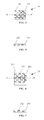
- Figures 4-5 illustrate an exemplary bonding pad structure consistent with the disclosed embodiments.
- Figure 5 is a cross-sectional view of the structure illustrated in Figure 4 along the AA' direction.
- the bonding pad structure may be made of a first metal material and a second metal material.
- the bonding pad structure 10 may include a plurality of first metal blocks 101 and a plurality of second metal blocks 102. On a top viewing plane, the plurality of first metal blocks 101 and the plurality of second metal blocks 102 may be distributed into rows and columns.
- the plurality of first metal blocks 101 may be made of the first metal material; and the plurality of second metal blocks 102 may be made of the second metal material.
- one second metal block 102 may be disposed between two adjacent first metal blocks 101; and one first metal block 101 may be disposed between two adjacent second metal blocks 102.
- one second metal block 102 may be disposed between two adjacent first metal blocks 101; and one first metal block 101 may be disposed between two adjacent second metal blocks 102.
- Such a uniform row and column distribution e.g., a checker formation
- the number of the first metal blocks 101 and the number of the second metal blocks 102 may be any appropriate value.
- the cross-sectional plane along the AA' direction may be perpendicular to the top viewing plane of the bonding pad structure 10. Further, the cross-sectional plane may divide the bonding pad structure 10 into to two equal parts. Thus, the cross-sectional plane may be a perpendicular and equal dividing plane.
- the cross-sectional plane illustrated in Figure 5 may be an equal dividing cross-sectional plane.
- the equal dividing cross-sectional plane may be obtained by crossing the bonding pad structure 10 along a perpendicular equal dividing plane.
- the perpendicular equal dividing plane may be perpendicular to the top viewing plane of the bonding pad structure 10. Further, the perpendicular equal dividing plane may be able to divide the bonding pad structure 10 into two equal parts.
- the bonding pad structure 10 at the cross-sectional plane illustrated in Figure 5 may show three first metal blocks 101 and three second metal blocks 102. That is, the first metal material may be shown three times and the second metal material may be shown three times in the cross-sectional viewing plane illustrated in Figure 5 .
- the outer metal material may all be the first metal material.
- the second metal material may be selected from the metal material having a relatively good ductility; and the first metal material may be selected from the metal material having a moderate ductility. Such selections of the metal materials may be able to use the first metal material to protect the second metal material.
- the first metal material and the second metal material may be any appropriate material.
- the first metal material is Ge; and the second metal material is Al.
- Ge may have a moderate ductility, and thus Ge itself may not be squeezed out and extended. Further, Ge may be able to form a GeAl alloy with Al that has a relatively good performance.
- the conductivity of Al may be relatively good; and the ductility of the Al may be relatively good. Such properties may facilitate Al and Ge to have an enough contact during the bonding process. Accordingly, it may ensure to thoroughly form AlGe alloy during the bonding process; and to form a sturdy bonding structure.
- the bonding pad structure 10 may have a plurality of first metal blocks 101 and a plurality of second metal blocks 102, during the subsequent process for bonding the bonding pad structure 10 with another bonding pad structure 10, or other bonding pad structures, the plurality of first meal blocks 101 and the plurality of second metal blocks 102 may directly form metal alloy. That is, the first metal material and the second metal material may directly form the metal alloy. Further, the first metal blocks 101 and the second metal blocks 102 may be alternatively distributed. Thus, it may be able to prevent the first metal blocks 101 and the second metal blocks from excessively overflowing around the bonding pad structure 10. Even the first metal blocks 101 and the second metal block 102 may overflow, the overflow amount may be acceptable.
- the first metal material of the bonding pad structure 10 on the first semiconductor structure and the second metal material of the bonding pad structure 10 on the second semiconductor structure may form a metal alloy.
- the first metal material of the bonding pad structure 10 on the second semiconductor structure and the second metal material of the bonding pad structure 10 on the first semiconductor structure may form a metal alloy.
- the metal alloys may bond the two semiconductor structures together. That is, one of the major functions of the metal alloys may be to bond the two semiconductor structures together.
- the first metal blocks 101 and the second metal blocks 102 in each semiconductor structure may also form meal alloy.
- the overflow of the first metal material having a relatively good ductility or the second metal having a relatively good ductility may be prevented. That is, using the bonding pad structure 10 to perform a bonding process, the bonding pad structure 10 may prevent the squeezing out and extending issue. Accordingly, the short-circuit between the bonding pad structure 10 and the surrounding conductive structures may be prevented.
- the reliability of the packaging structure having the disclosed bonding pad structure 10 may be improved.
- Figures 6-7 illustrate another exemplary bonding pad structure consistent with the disclosed embodiments.
- Figure 7 is a cross-sectional view of the structure illustrated in Figure 6 along the BB' direction.
- the bonding pad structure may be made of a first metal material and a second metal material.
- the bonding pad structure 20 may include a plurality of first metal blocks 201 and a plurality of second metal blocks 202.
- the plurality of first metal blocks 201 and the plurality of second metal blocks 202 may be distributed into rows and columns.
- the plurality of first metal blocks 201 may be made of the first metal material; and the plurality of second metal blocks 202 may be made of the second metal material.
- the bonding pad structure 20 may also include two first metal stripes 203.
- the plurality of first metal blocks 201 and the plurality of second metal blocks 202 may present as a rectangle as a whole.
- the two first metal stripes 203 may be disposed at two parallel sides of the rectangle. That is, the rectangle may be in between the two first metal stripes 203; and the two first metal stripes 203 may be able to protect the rectangle.
- first metal stripe when the plurality of first metal blocks 201 and the plurality of second metal blocks 202 present as a rectangle as a whole, one first metal stripe may be disposed outside any side of the rectangle; or three first metal stripes may be disposed outside of any three sides of the rectangle, respectively; or four first meal stripes may be disposed outside of all sides of the rectangle, respectively.
- first metal stripes when the plurality of first metal blocks 201 and the plurality of second metal blocks 202 present as other shapes as a whole, first metal stripes may be disposed outside of one or more sides of the shape. For example, when the plurality of first metal blocks 201 and the plurality of second metal blocks 202 present as a hexagon as a whole, one or more metal stripes may be disposed outside of one or more of the six sides of the hexagon, respectively.
- first metal blocks 201 and two second block 202 may be shown in the cross-sectional plane shown in Figure 7 . That is, the first metal material and the second metal material may be shown twice, respectively; and the first metal material and the second metal material may be alternatively shown.
- the first metal material and the second metal material may be shown one time, respectively, or a plurality of times, respectively.
- the equal dividing plane may be obtained by crossing the bonding pad structure 20 along a perpendicular equal dividing plane.
- the perpendicular equal dividing plane may be perpendicular to the top viewing plane of the bonding pad structure 20. Further, the perpendicular equal dividing plane may be able to divide the bonding pad 10 into two equal parts.
- the cross-sectional plane along the BB' is perpendicular to the top viewing plane of the bonding pad structure 20; and the cross-sectional plane may divide the bonding pad structure 20 into two equal parts.
- the cross-sectional plane may belong to the perpendicular equal dividing plane. That is, the cross-sectional plane illustrated in Figure 7 may be an equal dividing plane.
- the first metal material and the second metal material may be any appropriate material.
- the first metal material is Ge; and the second metal material is Al.
- the bonding pad structure may be made of a first metal material and a second metal material.
- the bonding pad structure 30 may include a plurality of first metal blocks 301 and a plurality of second metal blocks 302. On a top viewing plane, the plurality of first metal blocks 301 and the plurality of second metal blocks 302 may be distributed into rows and columns.
- the plurality of first metal blocks 301 may be made of the first metal material; and the plurality of second metal blocks 302 may be made of the second metal material.
- one second metal block 302 may be disposed between two adjacent first metal blocks 301; and one first metal block 301 may be disposed between two adjacent second metal blocks 302.
- one second metal block 302 may be disposed between two adjacent first metal blocks 301; and one first metal block 301 may be disposed between two adjacent second metal blocks 302.
- Such a uniform row and column distribution may facilitate the subsequent bonding of the bonding pad structure 30.
- the number of the first metal blocks 301 and the number of the second metal block 302 may be any appropriate value.
- the first metal material and the second metal material may be any appropriate material.
- the first metal material is Ge; and the second metal material is Al.
- the bonding pad structure may be made of a first metal material and a second metal material.
- the bonding pad structure 40 may include a first part.
- the first part is the bonding pad structure 40 itself.
- the first part may include a plurality of first metal stripes 401 and a plurality of second metal stripes 402.
- the first metal stripes 401 and the second metal stripes 402 may be elongated first metal blocks and elongated second metal blocks.
- the plurality of first metal stripes 401 and the plurality of second metal stripes 402 may be alternatively distributed.
- the plurality of first metal stripes 401 may be made of the first metal material; and the plurality of second metal stripes 402 may be made of the second metal material.
- the first metal stripes 401 may be shown four times; and the second metal stripes 402 may be shown three times. That is, the first metal material may be shown four times and the second metal material may be shown three times. In certain other embodiments, the first metal material and the second metal material may be shown with any appropriate number of times.
- the cross-sectional plane along the DD' direction may be perpendicular to the top viewing plane of the bonding pad 40. Further, the cross-sectional plane may divide the bonding pad structure 40 into to two equal parts.
- the cross-sectional plane may be a perpendicular and equal dividing plane. That is, the cross-sectional plane illustrated in Figure 11 may be an equal dividing plane.
- the equal dividing plane may be obtained by crossing the bonding pad structure 40 along the perpendicular equal dividing plane.
- the perpendicular equal dividing plane may be perpendicular to the top viewing plane of the bonding pad structure 40. Further, the perpendicular equal dividing plane may be able to divide the bonding pad structure 40 into two equal parts.
- the first metal material and the second metal material may be any appropriate material.
- the first metal material is Ge; and the second metal material is Al.
- the bonding pad structure 40 may have a plurality of alternatively distributed first metal stripes 401 and second metal stripes 402, during the subsequent process for bonding the bonding pad structure 40 with other bonding pad structures, the plurality of the first meal stripes 401 and the plurality of second metal stripes 402 may form metal alloy with each other.
- it may be able to prevent the second metal stripes 402 from excessively overflowing around the bonding pad structure 40. Accordingly, the squeezing out and extending issue may be prevented; and the short-circuit between the bonding pad structure 40 and the surrounding conductive structures may be prevented; and the reliability of the packaging structure formed by using the disclosed bonding pad structure 40 may be improved.
- Figures 12-13 illustrate another exemplary bonding pad structure consistent with the disclosed embodiments.
- Figure 13 is a cross-sectional view of the structure illustrated in Figure 12 along the EE' direction.
- the bonding pad structure may be made of a first metal material and a second metal material.
- the bonding pad structure 50 may include a first part.
- the first part is a portion of the bonding pad structure 50.
- the first part may include a plurality of first metal stripes 501 and a plurality of second metal stripes 502.
- the plurality of first metal stripes 501 and the plurality of second metal stripes 502 may be alternatively distributed.
- the plurality of first metal stripes 501 may be made of the first metal material; and the plurality of second metal stripes 502 may be made of the second metal material.
- the bonding pad structure 50 may also include a first metal ring 503.
- the first metal ring 503 may enclose the first part.
- the first meal stripes 501 and the second metal stripes 502 as a whole may be a rectangle.
- the first metal ring 503 may have a rectangular shape surrounding the first part. In certain other embodiments, when the first part has other shapes, the shape of the first metal ring 503 may change accordingly.
- the first metal stripes 501 may be shown three times; and the second metal stripes 502 may be shown four times.
- the first metal ring may be made of the first metal material.
- the first metal material may be shown five times and the second metal material may be shown four times.
- the first metal material and the second metal material may be shown with any appropriate number of times.
- the cross-sectional plane along the EE' direction may be perpendicular to the top viewing plane of the bonding pad 50. Further, the cross-sectional plane may divide the bonding pad 50 into to equal parts.
- the cross-sectional plane may be a perpendicular and equal dividing plane. That is, the cross-sectional plane illustrated in Figure 13 may be an equal dividing cross-sectional plane.
- the equal dividing plane may be obtained by crossing the bonding pad 50 along the perpendicular equal dividing plane.
- the perpendicular equal dividing plane may be perpendicular to the top viewing plane of the bonding pad structure 50. Further, the perpendicular equal dividing plane may be able to divide the bonding pad structure 50 into two equal parts.
- the bonding pad structure 50 may have a plurality of alternatively distributed first metal stripes 501 and second metal stripes 502, and the first metal ring 503, during the subsequent process for bonding the bonding pad structure 50 with other structures, the plurality of the first meal stripes 501 and the plurality of second metal stripes 502 and the first metal ring 503 may form metal alloy with each other.
- it may be able to prevent the first metal stripes 501 and the second metal stripes 502 from excessively overflowing around the bonding pad structure 50. Accordingly, the squeezing out and extending issue may be prevented; and the short-circuit between the bonding pad structure 50 and the surrounding conductive structures may be prevented; and the reliability of the packaging structure formed by using the disclosed bonding pad structure 50 may be improved.
- Figures 14-15 illustrate another exemplary bonding pad structure consistent with the disclosed embodiments.
- Figure 15 is a cross-sectional view of the structure illustrated in Figure 14 along the FF' direction.
- the bonding pad structure may be made of a first metal material and a second metal material.
- the bonding pad structure 60 may include a metal plate 601 and a metal ring 602.
- the metal ring 602 may be embedded into the metal plate 601.
- the metal plate 601 may be made of the first metal material; and the metal ring 602 may be made of the second metal material.
- the metal plate 601 may be shown three times; and the metal ring 602 may be shown two times That is, the first metal material may be shown three times; and the second metal material may be shown two times. In certain other embodiments, the first metal material and the second metal material may be shown with any appropriate number of times.
- the cross-sectional plane along the FF' direction may be perpendicular to the top viewing plane of the bonding pad 60. Further, the cross-sectional plane may divide the bonding pad 60 into to equal parts.
- the cross-sectional plane may be a perpendicular and equal dividing plane. That is, the cross-sectional plane illustrated in Figure 15 may be an equal dividing plane.
- the equal dividing plane may be obtained by crossing the bonding pad structure 60 along the perpendicular equal dividing plane.
- the perpendicular equal dividing plane may be perpendicular to the top viewing plane of the bonding pad structure 60. Further, the perpendicular equal dividing plane may be able to divide the bonding pad structure 60 into two equal parts.
- the first metal material and the second metal material may be made of any appropriate material.
- the first metal material is Ge; and the second metal material is Al.
- the bonding pad structure 60 may have a metal plate 601 and a metal ring 602. Further, on the top viewing plane of the bonding pad structure 60, the metal ring 602 may be embedded in the metal plate 601. Therefore, during the subsequent process for bonding the bonding pad structure 60 with other structures, the metal ring 602 with a better ductility may directly form metal alloy with the metal plate 601. Thus, the metal ring 602 may not overflow around the bonding pad structure 60. Accordingly, the squeezing out and extending issue may be prevented; the short-circuit between the bonding pad structure 60 and the surrounding conductive structures may be prevented; and the reliability of the packaging structure formed by using the disclosed bonding pad structure 60 may be improved.
- Figure 24 illustrates an exemplary MEMS device packaging process consistent with the disclosed embodiments.
- Figure 16 illustrates a structure corresponding to certain stages of the exemplary MEMS packaging process.
- a MEMS device wafer is provided (S101).
- Figure 16 illustrates a corresponding structure.
- an MEMS device wafer 310 is provided.
- the MEMS device wafer 310 may have a first bonding surface 310A.
- a cover plate wafer 320 may be provided (S102).
- the cover plate wafer 320 may have a second bonding surface 320A.
- control circuit there is no control circuit on the cover plate wafer 320. That is, no control circuit is formed on the cover plate wafer 320. In certain other embodiments, appropriate control circuits may be formed on the cover plate wafer 320.
- a plurality of first bonding pad structures 311 may be formed on the first bonding surface 310A; and a plurality of second bonding pad structures 321 may be formed on the second bonding surface 320A (S103).
- the cross-sectional plane of first the bonding pad structures 311 may be an equal dividing plane.
- the definition of the equal dividing plane may be similar to the previously described ones.
- one first bonding pad structure 311 may have four first metal blocks 3111 and three second metal blocks 3112.
- the first bonding pad structures 311 may be one or more of the disclosed bonding pad structures described previously.
- one second bonding pad structure 321 may have two third metal blocks 3211 and one fourth metal block 3212.
- the second bonding pad structures 321 may be one or more of the disclosed bonding pad structures described previously.
- the MEMS device wafer 310 and the cover plate wafer 320 may be bonded together using the first bonding structures 311 and the second bonding pad structures 321 (S104).
- the alloy formed between the first metal blocks 3111 and the fourth metal blocks 3212 and the alloy formed between the third metal blocks 3211 and the second metal blocks 3112 may provide the major bonding functions. Further, the alloy process between the first metal blocks 3111 and the second metal blocks 3112 and the alloy process between the third metal blocks 3211 and the fourth metal blocks 3212 may also facilitate the bonding process between the MEMS device wafer 310 and the cover plate wafer 320.
- the alignment between the first metal blocks 3111 and the fourth metal blocks 3212 may not be considered.
- the alignment between the third metal blocks 3211 and the second metal blocks 3112 may not be considered. That is, the alignments between the first bonding pad structures 311 and the second bonding pad structures 321 may not affect the bonding between the MEMS device wafer 310 and the cover plate wafer 320.
- the first metal material is Ge; and the second metal material is Al.
- the temperature of the bonding process is approximately 424°C
- Ge and Al may be able to form GeAl alloy with an atomic ratio of 1:1. Under such a condition, the mass ratio between Ge and Al is:
- the conductivity of the first bonding pad structures 311 may not be considered.
- the ratio of Al may be decreased; and the ratio of Ge may be increased. Accordingly, during the bonding process, Al may entirely consumed; and the overflowing of Al may be further prevented. Therefore, when the first bonding pad structures 311 is not electrically connected with the circuit structures on the MEMS device wafer 310, the mass ratio between the first metal material and the second metal material in the first bonding pad structures 311 may be in a range of approximately 0.59-0.71.
- the conductivity of the first bonding pad structures 311 may be appropriately increased. That is, the ratio of Ge may be decreased; and the ratio of Al may be increased. However, the ratio of Al may be controlled within an appropriate range to prevent the overflowing of Al.
- the mass ratio between the first metal material and the second metal material in the first bonding pad structures 311 may be in a range of approximately 0.47-0.59.
- circuit structures may be formed on the cover plate wafer 320.
- the mass ratio between the first metal material and the second metal material in the second bonding pad structures 321 may be in a range of approximately 0.59-0.71.
- the mass ratio between the first metal material and the second metal material in the second bonding pad structures 321 may be in a range of approximately 0.47-0.59.
- the method may also include thinning the MEMS device wafer 310 and the cover plate wafer 320; and dicing the individual MEMS device units in the MEMS device wafer 310.
- the sealing units in the cover plate unit 320 may also be diced.
- packaged MEMS devices may be formed.
- the second metal material that has a relatively good ductility may not easily overflow.
- the squeezing out and extending issue during the bonding process of the bonding pad structures may be prevented. Accordingly, the short-circuit issue among adjacent bonding pad structures may be avoided; and the reliability of the packaging structures may be improved.
- first bonding pad structures 311 and the second bonding pad structures 321 may be formed on the corresponding bonding surfaces directly; and it may not require to form protruding structures or trenches, etc.
- the process steps of the packaging structure may be simplified. Accordingly, the process time of the packaging method may be shortened; and the cost of the packaging process may be reduced.
- Figures 17-18 illustrate an exemplary bonding ring structure consistent with the disclosed embodiments.
- Figure 17 is the top view of the bonding ring structure; and
- Figure 18 is a cross-sectional view of the bonding ring structure illustrated in Figure 17 along the GG' direction.
- the bonding ring structure 70 may include a plurality of bonding pad units 700.
- the structure enclosed by the dotted line may refer to one bonding pad unit 700.
- the bonding pad unit 700 may be made of a first metal material and a second metal material.
- each of the bonding pad units 700 may include a plurality of first metal blocks 701 and a plurality of second metal blocks 702.
- the plurality of first metal blocks 701 and the plurality of second metal blocks 702 may be distributed into rows and columns.
- the plurality of first metal blocks 701 may be made of the first metal material; and the plurality of second metal blocks 702 may be made of the second metal material.
- one second metal block 702 may be disposed between two adjacent first metal blocks 701; and one first metal block 701 may be disposed between two adjacent second metal blocks 702.
- one second metal block 702 may be disposed between two adjacent first metal blocks 701; and one first metal block 701 may be disposed between two adjacent second metal blocks 702.
- the bonding pad unit 700 at the cross-sectional plane illustrated in Figure 18 may show three first metal blocks 701 and two second metal blocks 702. That is, three portions of first metal material and two portions of the second metal material may be shown in the cross-sectional view illustrated in Figure 18 .
- the bonding pad units 700 may also include one or more of the disclosed bonding pad structures illustrated in Figures 6-15 .
- the bonding ring structure 70 may include a plurality of disclosed bonding pad structures illustrated in Figures 6-15 , and may be distributed with any appropriate patterns and sequences, etc.
- the bonding pad units 700 may include a plurality of first metal blocks 701 and a plurality of second metal blocks 702, during the subsequent process for bonding the bonding ring structure 70 with other structures, the plurality of first meal blocks 701 and the plurality of second metal blocks 702 may directly form metal alloy. That is, the first metal material and the second metal material may directly form metal alloy. Further, the first metal blocks 701 and the second metal blocks 702 may be alternatively distributed. Thus, it may be able to prevent the first metal blocks 701 and the second metal blocks 701 from excessively overflowing around the bonding ring structure 70.
- the overflow amount may be acceptable. Therefore, when the bonding ring structure 70 is used for a bonding process, the squeezing out and extending process may be prevented; and the short-circuit issue between the bonding ring structure 70 and the surrounding conductive structures may be prevented; and the reliability of the packaging structure using the bonding ring structure 70 may be improved.
- Figure 25 illustrates another exemplary packaging method of MEMS structures.
- Figures 19-23 illustrate structures corresponding certain stages of the exemplary packaging method.
- an MEMS device wafer is provided (S201).
- Figure 19 illustrates a corresponding structure.
- an MEMS device wafer 400 is provided.
- the MEMS device wafer 400 may have a first bonding surface (not labeled). Further, a first metal material layer 4001 may be formed on the first bonding surface.
- the first metal material layer 4001 may be made of any appropriate material, such as Ge, etc.
- Various processes may be used to form the first metal material layer 4001, such as a physical vapor deposition (PVD) process, a sputtering process, or an electroplating process, etc.
- PVD physical vapor deposition
- a plurality of first metal blocks may be formed (S202).
- Figure 20 illustrates a corresponding structure.
- a plurality of first metal blocks 401 are formed on the surface of the MEMS device wafer 400.
- the plurality of first metal blocks 401 may be formed by etching the first metal material layer 4001.
- a plurality of trenches (not labeled) may be also be formed among the plurality of first metal blocks 401.
- the plurality of trenches may be used to subsequently form second metal blocks.
- the first metal material layer 4001 may be etched by any appropriate process, such as a dry etching process, a wet etching process, or an ion beam etching process, etc. Before the etching process, a patterned mask layer may be formed on the first metal layer 4001. The patterned mask layer may be used as an etching mask.
- a second metal layer may be formed (S203).
- Figure 21 illustrates a corresponding semiconductor structure.
- a second metal material layer 4002 is formed on the first bonding surface of the MEMS device wafer 400.
- the second metal material layer 4002 may cover the first metal blocks 401, and fill the plurality of the trenches.
- the second metal material layer 4002 may be made of any appropriate material, such as Al, etc.
- Various processes may be used to form the second metal material layer, such as a PVD process, a sputtering process, or a chemical plating process, etc.
- a planarization process may be performing (S204).
- Figure 22 illustrates a corresponding structure.
- a planarization process may be performed to remove portions of the second metal material layer 4002 higher than the first metal blocks 401. That is, the planarization process may be performed until the top surfaces of the first metal blocks 401 are exposed.
- the planarization process may be any appropriate process, such as a chemical mechanical polishing process, or a physical mechanical polishing process, etc.
- a plurality of second metal blocks may be formed (S205).
- Figure 23 illustrates a corresponding structure.
- portions of the planarized second metal material layer 4002 may be removed; and a plurality of second metal blocks 402 may be formed.
- a plurality of second metal blocks 402 and a plurality of first metal blocks 401 may form one bonding ring structure 410.
- one or more bonding ring structures 410 may be formed on the MEMS device wafer 400.
- the portions of the planarized second metal material layer 4002 may be removed by any appropriate process, such as a dry etching process, or a wet etching process, etc.
Landscapes
- Engineering & Computer Science (AREA)
- Microelectronics & Electronic Packaging (AREA)
- Manufacturing & Machinery (AREA)
- Micromachines (AREA)
- Internal Circuitry In Semiconductor Integrated Circuit Devices (AREA)
- Wire Bonding (AREA)
Abstract
Description
- This application claims the priority of Chinese patent application No.
201510614165.2, filed on September 23, 2015 - The present invention generally relates to the field of semiconductor manufacturing and, more particularly, relates to bonding pad structures, bonding ring structures and MEMS device packaging processes.
- Micro-Electro-Mechanical-System (MEMS), also referred as micro-system or micro-machine, is a high-tech type of electro-mechanical system. MEMS devices are developed based upon microelectronic technologies and semiconductor manufacturing technologies. MEMS devices are formed by the combination of the thin film technology, the photolithography technology, the bonding technology, the silicon micromachining technology, the non-silicon micromachining technology, and the precise micromachining technology, etc. MEMS devices include a plurality of types of devices, such as MEME sensors and MEMS actuators, etc. Among MEMS devices, the MEMS sensors have been widely used in the protection systems of automobile, inertia control system, home appliance, and various kinds of apparatus, and the systems of many other industries, scientific and engineering systems, etc. Specifically, the MEMS sensors include accelerating sensors, pressure sensors, vibrational gyroscopes, and micro-relays, etc.
- A MEMS device needs a cavity to isolate the effects from external environments. To form such a cavity, it needs to bond the substrate of the MEMS device with a cover plate. The bonding process includes the silicon-silicon direct bonding process, the eutectic bonding process, the silicon alloy bonding process, or the glass frit bonding process, etc. Among such bonding processes, the eutectic bonding process has certain advantages, such as high efficiency and high packaging performance, etc.
- During the eutectic bonding process, it often needs a bonding pad structure or a bonding ring structure.
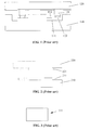
Figure 1 illustrates an exemplary MEMS packaging structure. - As shown in
Figure 1 , the MEMS packaging structure includes aMEMS device substrate 110, and acover plate substrate 120. TheMEMS device substrate 110 includes a passivation layer. Some parts of the MEMS device substrate are omitted inFigure 1 , and the passivation layer is not labeled. The passivation layer is partially etched to formtrenches 112. The bottoms of thetrenches 112 exposebonding pads 111.Protruding structures 121 are formed on thecover plate substrate 120. Further, ametal layer 122 is formed on the top surfaces of theprotruding structures 121. During the packaging process, themetal layer 122 and thebonding pads 111 are fused together to form a metal alloy; and themetal layer 122 and thebonding pads 111 are bonded together. One of the purposes for forming theprotruding structures 121 is to enable themetal layer 122 to reach the bottoms of thetrenches 112 to contact with thebonding pads 111. One of the purposes to form thetrenches 112 is to prevent the squeezing out and extending of the material of thebonding pads 111. - However, forming the
protruding structures 121 and thetrenches 112 increases process steps, process time and production cost, etc. Further, theprotruding structures 121 are easily damaged; and the reliability of the packaging structure is reduced. -
Figure 2 illustrates an existing MEMS packaging method. As shown inFigure 2 ,bonding pads 221 are formed on the bonding surface of the MEMS device wafer 210 directly without forming trenches. Then, bondingpads 221 are formed on the bonding surface of thecover plate wafer 220. Then, thebonding pads 211 and thebonding pads 221 are bonded together (not shown) to package theMEMS device wafer 210 and the cover plate wafer 220 together (not shown). - As shown in
Figure 3 , thebonding pads 211 are made of one metal material. That is, the top view of thebonding pad 211 is a complete coverage structure. The structures of thebonding pads 221 are usually identical to the structures of thebonding pads 211. At least one of the metal material of thebonding pads 221 and the metal material of thebonding pads 211 has a relatively good ductility to facilitate the eutectic bonding process. When thebonding pads 211 having the complete coverage structure illustrated inFigure 3 are used, it may be easy for the material having the relatively good ductility to be squeezed out and stretched during the bonding process. That is, during the bonding process, the material having the relatively good ductility overflows to the surrounding regions of thebonding pads 211. When the metal material overflows in the surrounding regions of the bonding pads with a relatively large amount, it may be easy to cause the adjacent conductive structures and the bonding pads to have a short-circuit issue. Accordingly, the reliability of the packaging structure may be reduced. - The disclosed device structures and methods are directed to solve one or more problems set forth above and other problems in the art.
- One aspect of the present disclosure includes a bonding pad structure. An exemplary bonding pad structure includes a plurality of first metal blocks made of a first metal material; and a plurality of second metal block made of a second metal material. On at least one equal dividing plane of the bonding pad structure, the first metal material is shown at least one time; and the second metal material is shown at least one time. The first metal blocks are configured to prevent the squeezing out of the second metal blocks.
- Another aspect of the present disclosure includes a method for packaging MEMS devices. The method includes providing a MEMS device wafer having a first bonding surface; providing a cover plate wafer having a second bonding surface; forming at least one bonding pad structure having a plurality of first metal blocks made of a first metal material and a plurality of second metal blocks made of a second metal material on at least one of the first bonding surface and the second bonding surface; and bonding the MEMS device wafer and the cover plate wafer using the at least one bonding pad structure. The first metal blocks are configured to prevent the squeezing out of the second metal blocks.
- Another aspect of the present disclosure includes a method for packaging MEMS devices. The method includes providing an MEMS device wafer having a first bonding surface; providing a cover plate wafer having a second bonding surface; forming at least one bonding ring structure made of a first metal material and a second metal material on at least one of the first bonding surface and the second bonding surface; and bonding the MEMS device wafer and the cover plate wafer using the at least one bonding ring structure.
- In one embodiment the bonding pad structure comprises a plurality of first metal blocks made of a first metal material; and a plurality of second metal block made of a second metal material, wherein the plurality of first metal blocks are used to protect squeezing out and extending of the second metal blocks; and on at least one equal dividing plane of the bonding pad structure the first metal material is shown at least one time and the second metal material is shown at least one time.
- In the bonding pad structure, on top viewing plane (i.e. in a plane defined by a top view on the bonding pad structure), the plurality of first metal blocks and the plurality of second metal blocks may be distributed into columns and rows alternatively; wherein one second metal block is disposed between two adjacent first metal blocks in each row; and wherein one first metal block is disposed between two adjacent second metal blocks in each column.
- Additionally, the bonding pad structure may further comprise a first metal ring enclosing the plurality of first metal blocks and the second metal blocks on a top viewing plane of the bonding pad structure.
- In the bonding pad structure the plurality of first metal blocks may be a plurality of first metal stripes; the plurality of second metal blocks may be a plurality of metal stripes; and the plurality of first metal stripes and the plurality of second metal stripes may be distributed alternatively on a top viewing plane of the bonding pad structure.
- Additionally, the bonding pad structure may further comprise a first metal ring enclosing the first metal stripes and the second metal stripes on a top viewing plane.
- In the bonding pad structure the plurality of first metal blocks may include a metal plate; the plurality of second metal blocks may include a metal ring; and the metal ring may be embedded in the first metal plate on a top viewing plane of the bonding pad structure.
- In the bonding pad structure the first metal material may be Ge; and the second metal material may be Al.
- In the bonding pad structure, on at least one equal dividing plane, the first metal material and the second metal material may be shown alternatively; and most outer sides of the equal dividing plane are the first metal material.
- It is noted, the equal dividing plane is defined to cross the bonding pad structure along a perpendicular equal dividing plane, wherein the perpendicular equal dividing plane is perpendicular to the top viewing plane of the bonding pad structure and the perpendicular equal dividing plane divides the bonding pad into two equal parts.
- A plurality of the bonding pad structures may be arranged to form a bonding ring structure. That is to say, the bonding ring structure comprise a plurality of the bonding pad structures. In the bonding ring structure the plurality of bonding pad structures may be distributed into a rectangular ring.
- The method for packaging MEMS devices may comprise providing a MEMS device wafer having a first bonding surface; providing a cover plate wafer having a second bonding surface; forming at least one bonding pad structure according to the invention (which comprises a plurality of first metal blocks made of the first metal material and a plurality of second metal blocks made of the second metal material) on at least one of the first bonding surface and the second bonding surface; and bonding the MEMS device wafer and the cover plate wafer using the at least one bonding pad structure. Thus, the first metal blocks can prevent squeezing out and extending of the plurality of second metal blocks.
- In the method, the plurality of first metal blocks made of the first metal material and the plurality of second metal blocks made of the second metal material may be arranged such that the first metal material is shown at least one time on at least one equal dividing plane of the bonding pad structure; and the second metal material is shown at least one time on at least one equal dividing plane of the bonding pad structure.
- In the method, the first metal material may be made of Ge; and the second metal material may be made of Al.
- In the method, if the at least one bonding pad structure is not electrically connected with circuit structures on one or more of the MEMS device wafer and the cover plate wafer, a mass ratio between the first metal material and the second metal material is preferably in a range of approximately 0.59-0.71.
- In the method, if the at least one bonding pad structure is electrically connected with circuit structures on one or more of the MEMS device wafer and the cover plate wafer, a mass ratio between the first metal material and the second metal material is preferably in a range of approximately 0.47-0.59.
- The method for packaging MEMS devices may comprise forming at least one bonding ring structure with a plurality of the bonding pad structure according to the invention (so that the bonding ring structure comprises a plurality of first metal blocks made of a first metal material and a plurality of second metal blocks made of a second metal material) on at least one of the first bonding surface and the second bonding surface; and bonding the MEMS device wafer and the cover plate wafer using the at least one bonding ring structure. Thus, the plurality of first metal blocks can prevent the squeezing out and extending of the plurality of second metal blocks.
- In the method, the at least one bonding ring structure may include a plurality of bonding pad units; the bonding pad units may be formed by a bonding pad structure according to the invention (thus, a bonding pad unit includes the plurality of first metal blocks made of the first metal material and the plurality of second metal blocks made of the second metal material). The first metal material may be shown at least one time on at least one equal dividing plane of each bonding pad unit. The second metal material may be shown at least one time on at least one equal dividing plane of each bonding pad unit.
- In the method, the first metal material may be made of Ge; and the second metal material may be made of Al.
- In the method, if the at least one bonding ring structure is not electrically connected with circuit structures on one or more of the MEMS device wafer and the cover plate wafer, a mass ratio between the first metal material and the second metal material is preferably in a range of approximately 0.59-0.71.
- In the method, if the at least one bonding ring structure is electrically connected with circuit structures on one or more of the MEMS device wafer and the cover plate wafer, a mass ratio between the first metal material and the second metal material is preferably in a range of approximately 0.47-0.59.
- Other aspects of the present disclosure can be understood by those skilled in the art in light of the description, the claims, and the drawings of the present disclosure.
-
-
Figure 1 illustrates an existing MEMS packaging structure; -
Figure 2 illustrates a structure corresponding to certain stages of an existing MEMS packaging method; -
Figure 3 illustrates a top view of one bonding pad of the structure illustrated inFigure 2 ; -
Figure 4 illustrates a top view of an exemplary bonding pad structure consistent with the disclosed embodiments; -
Figure 5 illustrates a cross-sectional view of the structure illustrated inFigure 4 along the AA' direction; -
Figure 6 illustrates a top view of another exemplary bonding pad structure consistent with the disclosed embodiments; -
Figure 7 illustrates a cross-sectional view of the structure illustrated inFigure 6 along the BB' direction; -
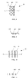
Figure 8 illustrates a top view of another exemplary bonding pad structure consistent with the disclosed embodiments; -
Figure 9 illustrates a cross-sectional view of the structure illustrated inFigure 8 along the CC' direction; -
Figure 10 illustrates a top view of another exemplary bonding pad structure consistent with the disclosed embodiments; -
Figure 11 illustrates a cross-sectional view of the structure illustrated inFigure 10 along the DD' direction; -
Figure 12 illustrates a top view of another exemplary bonding pad structure consistent with the disclosed embodiments; -
Figure 13 illustrates a cross-sectional view of the structure illustrated inFigure 12 along the EE' direction; -
Figure 14 illustrates a top view of another exemplary bonding pad structure consistent with the disclosed embodiments; -
Figure 15 illustrates a cross-sectional view of the structure illustrated inFigure 14 along the FF' direction; -
Figure 16 illustrates a structure corresponding to certain stages of an exemplary MEMS packaging method consistent with the disclosed embodiments; -
Figure 17 illustrates an exemplary bonding ring structure consistent with the disclosed embodiments; -
Figure 18 illustrates a cross-sectional view of a bonding ring unit of the structure illustrated inFigure 17 along GG' direction; -
Figures 19-23 illustrate structures corresponding to certain stages of another exemplary MEMS device packaging process consistent with the disclosed embodiments; -
Figure 24 illustrates an exemplary MEMS device packaging process consistent with the disclosed embodiments; and -
Figure 25 illustrates another exemplary MEMS device packaging process consistent with the disclosed embodiments. - Reference will now be made in detail to exemplary embodiments of the invention, which are illustrated in the accompanying drawings. Wherever possible, the same reference numbers will be used throughout the drawings to refer to the same or like parts.
-
Figures 4-5 illustrate an exemplary bonding pad structure consistent with the disclosed embodiments.Figure 5 is a cross-sectional view of the structure illustrated inFigure 4 along the AA' direction. - The bonding pad structure may be made of a first metal material and a second metal material. Specifically, as shown in
Figures 4-5 , thebonding pad structure 10 may include a plurality of first metal blocks 101 and a plurality of second metal blocks 102. On a top viewing plane, the plurality of first metal blocks 101 and the plurality of second metal blocks 102 may be distributed into rows and columns. The plurality of first metal blocks 101 may be made of the first metal material; and the plurality of second metal blocks 102 may be made of the second metal material. - In the top viewing plane illustrated in
Figure 4 , in one row, onesecond metal block 102 may be disposed between two adjacent first metal blocks 101; and onefirst metal block 101 may be disposed between two adjacent second metal blocks 102. In one column, onesecond metal block 102 may be disposed between two adjacent first metal blocks 101; and onefirst metal block 101 may be disposed between two adjacent second metal blocks 102. Such a uniform row and column distribution (e.g., a checker formation) may facilitate the subsequent bonding of thebonding pad structure 10 to another bonding pad structure. The number of the first metal blocks 101 and the number of the second metal blocks 102 may be any appropriate value. - In one embodiment, the cross-sectional plane along the AA' direction may be perpendicular to the top viewing plane of the
bonding pad structure 10. Further, the cross-sectional plane may divide thebonding pad structure 10 into to two equal parts. Thus, the cross-sectional plane may be a perpendicular and equal dividing plane. The cross-sectional plane illustrated inFigure 5 may be an equal dividing cross-sectional plane. The equal dividing cross-sectional plane may be obtained by crossing thebonding pad structure 10 along a perpendicular equal dividing plane. The perpendicular equal dividing plane may be perpendicular to the top viewing plane of thebonding pad structure 10. Further, the perpendicular equal dividing plane may be able to divide thebonding pad structure 10 into two equal parts. - In one embodiment, the
bonding pad structure 10 at the cross-sectional plane illustrated inFigure 5 may show three first metal blocks 101 and three second metal blocks 102. That is, the first metal material may be shown three times and the second metal material may be shown three times in the cross-sectional viewing plane illustrated inFigure 5 . - In certain other embodiments, in the at least one equal dividing plane, one
first metal block 101 and at least onesecond metal block 102 may be shown, or a plurality of first metal blocks 101 and a plurality of second metal blocks 102 may be shown. - In certain other embodiments, when the first metal material and the second metal material are shown alternatively, the outer metal material may all be the first metal material. Under such a configuration, the second metal material may be selected from the metal material having a relatively good ductility; and the first metal material may be selected from the metal material having a moderate ductility. Such selections of the metal materials may be able to use the first metal material to protect the second metal material.
- The first metal material and the second metal material may be any appropriate material. In one embodiment, the first metal material is Ge; and the second metal material is Al. Ge may have a moderate ductility, and thus Ge itself may not be squeezed out and extended. Further, Ge may be able to form a GeAl alloy with Al that has a relatively good performance. The conductivity of Al may be relatively good; and the ductility of the Al may be relatively good. Such properties may facilitate Al and Ge to have an enough contact during the bonding process. Accordingly, it may ensure to thoroughly form AlGe alloy during the bonding process; and to form a sturdy bonding structure.
- Thus, the
bonding pad structure 10 may have a plurality of first metal blocks 101 and a plurality of second metal blocks 102, during the subsequent process for bonding thebonding pad structure 10 with anotherbonding pad structure 10, or other bonding pad structures, the plurality of first meal blocks 101 and the plurality of second metal blocks 102 may directly form metal alloy. That is, the first metal material and the second metal material may directly form the metal alloy. Further, the first metal blocks 101 and the second metal blocks 102 may be alternatively distributed. Thus, it may be able to prevent the first metal blocks 101 and the second metal blocks from excessively overflowing around thebonding pad structure 10. Even the first metal blocks 101 and thesecond metal block 102 may overflow, the overflow amount may be acceptable. - Thus, when the bonding surfaces of two semiconductor structures, for example, two wafers, have the at least one
bonding pad structure 10, during the process for bonding the two semiconductor structures together, the first metal material of thebonding pad structure 10 on the first semiconductor structure and the second metal material of thebonding pad structure 10 on the second semiconductor structure may form a metal alloy. The first metal material of thebonding pad structure 10 on the second semiconductor structure and the second metal material of thebonding pad structure 10 on the first semiconductor structure may form a metal alloy. Thus, the metal alloys may bond the two semiconductor structures together. That is, one of the major functions of the metal alloys may be to bond the two semiconductor structures together. - The first metal blocks 101 and the second metal blocks 102 in each semiconductor structure may also form meal alloy. Thus, the overflow of the first metal material having a relatively good ductility or the second metal having a relatively good ductility may be prevented. That is, using the
bonding pad structure 10 to perform a bonding process, thebonding pad structure 10 may prevent the squeezing out and extending issue. Accordingly, the short-circuit between thebonding pad structure 10 and the surrounding conductive structures may be prevented. Thus, the reliability of the packaging structure having the disclosedbonding pad structure 10 may be improved. -
Figures 6-7 illustrate another exemplary bonding pad structure consistent with the disclosed embodiments.Figure 7 is a cross-sectional view of the structure illustrated inFigure 6 along the BB' direction. - The bonding pad structure may be made of a first metal material and a second metal material. Specifically, as shown in
Figures 6-7 , thebonding pad structure 20 may include a plurality of first metal blocks 201 and a plurality of second metal blocks 202. On a top viewing plane, the plurality of first metal blocks 201 and the plurality of second metal blocks 202 may be distributed into rows and columns. The plurality of first metal blocks 201 may be made of the first metal material; and the plurality of second metal blocks 202 may be made of the second metal material. - In the top view plane illustrated in
Figure 6 , in one row, onesecond metal block 202 may be disposed between two adjacent first metal blocks 201; and onefirst metal block 201 may be disposed between two adjacent second metal blocks 202. In one column, onesecond metal block 202 may be disposed between two adjacent first metal blocks 201; and onefirst metal block 201 may be disposed between two adjacent second metal blocks 202. Such a uniform row and column distribution may facilitate the subsequent bonding of thebonding pad structure 20. The number of the first metal blocks 101 and the number of thesecond metal block 102 may be any appropriate value. - Further, as shown in
Figure 6 , thebonding pad structure 20 may also include twofirst metal stripes 203. The plurality of first metal blocks 201 and the plurality of second metal blocks 202 may present as a rectangle as a whole. The twofirst metal stripes 203 may be disposed at two parallel sides of the rectangle. That is, the rectangle may be in between the twofirst metal stripes 203; and the twofirst metal stripes 203 may be able to protect the rectangle. - In certain other embodiments, when the plurality of first metal blocks 201 and the plurality of second metal blocks 202 present as a rectangle as a whole, one first metal stripe may be disposed outside any side of the rectangle; or three first metal stripes may be disposed outside of any three sides of the rectangle, respectively; or four first meal stripes may be disposed outside of all sides of the rectangle, respectively. In still certain other embodiments, when the plurality of first metal blocks 201 and the plurality of second metal blocks 202 present as other shapes as a whole, first metal stripes may be disposed outside of one or more sides of the shape. For example, when the plurality of first metal blocks 201 and the plurality of second metal blocks 202 present as a hexagon as a whole, one or more metal stripes may be disposed outside of one or more of the six sides of the hexagon, respectively.
- In one embodiment, in the cross-sectional plane shown in
Figure 7 , two first metal blocks 201 and twosecond block 202 may be shown. That is, the first metal material and the second metal material may be shown twice, respectively; and the first metal material and the second metal material may be alternatively shown. - In certain other embodiments, in an equal dividing plane of the
bonding pad structure 20, the first metal material and the second metal material may be shown one time, respectively, or a plurality of times, respectively. The equal dividing plane may be obtained by crossing thebonding pad structure 20 along a perpendicular equal dividing plane. The perpendicular equal dividing plane may be perpendicular to the top viewing plane of thebonding pad structure 20. Further, the perpendicular equal dividing plane may be able to divide thebonding pad 10 into two equal parts. In one embodiment, the cross-sectional plane along the BB' is perpendicular to the top viewing plane of thebonding pad structure 20; and the cross-sectional plane may divide thebonding pad structure 20 into two equal parts. Thus, the cross-sectional plane may belong to the perpendicular equal dividing plane. That is, the cross-sectional plane illustrated inFigure 7 may be an equal dividing plane. - The first metal material and the second metal material may be any appropriate material. In one embodiment, the first metal material is Ge; and the second metal material is Al.
- Besides the advantages of the
bonding pad structure 10 illustrated inFigure 4 , thebonding pad structure 20 may providing extra benefits. Because thebonding pad structure 20 may have twofirst metal stripes 203; and the twofirst metal stripes 203 may hold the parallel first metal blocks 201 and the second metal blocks 201 in between, during the subsequent bonding process, the second metal blocks 202 may not only be able to form metal alloy with first metal blocks 201, but also form metal alloy withfirst metal stripes 203. Therefore, except the most outer edges of thebonding pad structure 20 may have a less amount of second metal material, all other second metal blocks 202 may not be squeezed out to the surrounding area of thebonding pad structure 20. Thus, the squeezing out and extending issue may be further prevented. Accordingly, the short-circuit issue between thebonding pad structure 20 and the surrounding conductive structures may be further prevented; and the reliability of the packaging structure formed by using thebonding pad structure 20 may be further improved. -
Figures 8-9 illustrate another exemplary bonding pad structure consistent with the disclosed embodiments.Figure 9 is a cross-sectional view of the structure illustrated inFigure 8 along the CC' direction. - The bonding pad structure may be made of a first metal material and a second metal material. Specifically, as shown in
Figures 8-9 , thebonding pad structure 30 may include a plurality of first metal blocks 301 and a plurality of second metal blocks 302. On a top viewing plane, the plurality of first metal blocks 301 and the plurality of second metal blocks 302 may be distributed into rows and columns. The plurality of first metal blocks 301 may be made of the first metal material; and the plurality of second metal blocks 302 may be made of the second metal material. - In the top view plane illustrated in
Figure 8 , in one row, onesecond metal block 302 may be disposed between two adjacent first metal blocks 301; and onefirst metal block 301 may be disposed between two adjacent second metal blocks 302. In one column, onesecond metal block 302 may be disposed between two adjacent first metal blocks 301; and onefirst metal block 301 may be disposed between two adjacent second metal blocks 302. Such a uniform row and column distribution may facilitate the subsequent bonding of thebonding pad structure 30. The number of the first metal blocks 301 and the number of thesecond metal block 302 may be any appropriate value. - Further, as shown in
Figure 8 , thebonding pad structure 30 may also include ametal ring 303; and thefirst metal ring 303 may enclose the first metal blocks 301 and the second metal blocks302. In one embodiment, the plurality of first metal blocks 301 and the plurality of second metal blocks 302 as a whole may be a rectangle. Thus, thefirst metal ring 303 may be rectangular. In certain other embodiments, according to the different shapes of the plurality of first metal blocks 301 and second metal blocks 302 as a whole, thefirst metal ring 303 may have different shapes, such as a circle, an oval, a triangle, a square, or other polygons. - In one embodiment, in the cross-sectional plane shown in
Figure 9 , two first metal blocks 301 and twosecond blocks 302 may be shown. That is, the first metal material and the second metal material may be shown twice, respectively; and the first metal material and the second metal material may be alternatively shown. Further, two sides (metal stripes) of the rectangularfirst metal ring 303 may also be shown at two sides of the complete structure formed by the first metal blocks 301 and the second metal blocks 302. - In one embodiment, the
first metal ring 303 may be made of the first metal material. Thus, in the cross-sectional plane shown inFigure 9 , the first metal material may be shown four times and the second metal material may be shown two times. - The cross-sectional plane may be obtained by crossing the
bonding pad structure 30 along a perpendicular equal dividing plane. The perpendicular equal dividing plane may be perpendicular to the top viewing plane of thebonding pad structure 30. Further, the perpendicular equal dividing plane may be able to divide thebonding pad structure 30 into two equal parts. In one embodiment, the cross-sectional plane along the CC' is perpendicular to the top viewing plane of thebonding pad structure 30; and the cross-sectional plane may divide thebonding pad structure 30 into two equal parts. Thus, the cross-sectional plane may belong to the perpendicular equal dividing plane. That is, the cross-sectional plane illustrated inFigure 9 may be an equal dividing plane. - The first metal material and the second metal material may be any appropriate material. In one embodiment, the first metal material is Ge; and the second metal material is Al.
- Besides the advantages of the
bonding pad structure 10 illustrated inFigure 4 , thebonding pad structure 30 may provide extra benefits. Because thebonding pad structure 30 may have thefirst metal ring 303; and thefirst metal ring 303 encloses the parallel first metal blocks 301 and the second metal blocks 302, during the subsequent bonding process, the second metal blocks 302 may not only be able to form metal alloy with first metal blocks 301, but also form metal alloy with thefirst metal ring 303. Therefore, all the second metal blocks 202 may not be squeezed out to the surrounding area of thebonding pad structure 30. Thus, the squeezing out and extending issue may be further prevented. Accordingly, the short-circuit issue between thebonding pad structure 30 and the surrounding conductive structures may be further prevented; and the reliability of the packaging structure formed by using thebonding pad structure 30 may be further improved. -
Figures 10-11 illustrate another exemplary bonding pad structure consistent with the disclosed embodiments.Figure 11 is a cross-sectional view of the structure illustrated inFigure 11 along the DD' direction. - The bonding pad structure may be made of a first metal material and a second metal material. Specifically, as shown in
Figure 10 , thebonding pad structure 40 may include a first part. In one embodiment, the first part is thebonding pad structure 40 itself. The first part may include a plurality offirst metal stripes 401 and a plurality ofsecond metal stripes 402. Thefirst metal stripes 401 and thesecond metal stripes 402 may be elongated first metal blocks and elongated second metal blocks. On a top viewing plane, the plurality offirst metal stripes 401 and the plurality ofsecond metal stripes 402 may be alternatively distributed. The plurality offirst metal stripes 401 may be made of the first metal material; and the plurality ofsecond metal stripes 402 may be made of the second metal material. - In one embodiment, in a cross-sectional plane illustrated in
Figure 11 , thefirst metal stripes 401 may be shown four times; and thesecond metal stripes 402 may be shown three times. That is, the first metal material may be shown four times and the second metal material may be shown three times. In certain other embodiments, the first metal material and the second metal material may be shown with any appropriate number of times. - In one embodiment, the cross-sectional plane along the DD' direction may be perpendicular to the top viewing plane of the
bonding pad 40. Further, the cross-sectional plane may divide thebonding pad structure 40 into to two equal parts. Thus, the cross-sectional plane may be a perpendicular and equal dividing plane. That is, the cross-sectional plane illustrated inFigure 11 may be an equal dividing plane. The equal dividing plane may be obtained by crossing thebonding pad structure 40 along the perpendicular equal dividing plane. The perpendicular equal dividing plane may be perpendicular to the top viewing plane of thebonding pad structure 40. Further, the perpendicular equal dividing plane may be able to divide thebonding pad structure 40 into two equal parts. - The first metal material and the second metal material may be any appropriate material. In one embodiment, the first metal material is Ge; and the second metal material is Al.
- Thus, the
bonding pad structure 40 may have a plurality of alternatively distributedfirst metal stripes 401 andsecond metal stripes 402, during the subsequent process for bonding thebonding pad structure 40 with other bonding pad structures, the plurality of thefirst meal stripes 401 and the plurality ofsecond metal stripes 402 may form metal alloy with each other. Thus, it may be able to prevent thesecond metal stripes 402 from excessively overflowing around thebonding pad structure 40. Accordingly, the squeezing out and extending issue may be prevented; and the short-circuit between thebonding pad structure 40 and the surrounding conductive structures may be prevented; and the reliability of the packaging structure formed by using the disclosedbonding pad structure 40 may be improved. -
Figures 12-13 illustrate another exemplary bonding pad structure consistent with the disclosed embodiments.Figure 13 is a cross-sectional view of the structure illustrated inFigure 12 along the EE' direction. - The bonding pad structure may be made of a first metal material and a second metal material. Specifically, as shown in
Figure 12 , thebonding pad structure 50 may include a first part. In one embodiment, the first part is a portion of thebonding pad structure 50. The first part may include a plurality offirst metal stripes 501 and a plurality ofsecond metal stripes 502. On a top viewing plane, the plurality offirst metal stripes 501 and the plurality ofsecond metal stripes 502 may be alternatively distributed. The plurality offirst metal stripes 501 may be made of the first metal material; and the plurality ofsecond metal stripes 502 may be made of the second metal material. - Further, the
bonding pad structure 50 may also include afirst metal ring 503. On a top viewing plane, thefirst metal ring 503 may enclose the first part. In one embodiment, thefirst meal stripes 501 and thesecond metal stripes 502 as a whole may be a rectangle. Thefirst metal ring 503 may have a rectangular shape surrounding the first part. In certain other embodiments, when the first part has other shapes, the shape of thefirst metal ring 503 may change accordingly. - In one embodiment, in a cross-sectional plane illustrated in
Figure 13 , thefirst metal stripes 501 may be shown three times; and thesecond metal stripes 502 may be shown four times. In one embodiment, the first metal ring may be made of the first metal material. Thus, the first metal material may be shown five times and the second metal material may be shown four times. In certain other embodiments, the first metal material and the second metal material may be shown with any appropriate number of times. - In one embodiment, the cross-sectional plane along the EE' direction may be perpendicular to the top viewing plane of the
bonding pad 50. Further, the cross-sectional plane may divide thebonding pad 50 into to equal parts. Thus, the cross-sectional plane may be a perpendicular and equal dividing plane. That is, the cross-sectional plane illustrated inFigure 13 may be an equal dividing cross-sectional plane. The equal dividing plane may be obtained by crossing thebonding pad 50 along the perpendicular equal dividing plane. The perpendicular equal dividing plane may be perpendicular to the top viewing plane of thebonding pad structure 50. Further, the perpendicular equal dividing plane may be able to divide thebonding pad structure 50 into two equal parts. - The first metal material and the second metal material may be any appropriate material. In one embodiment, the first metal material is Ge; and the second metal material is Al.
- Thus, the
bonding pad structure 50 may have a plurality of alternatively distributedfirst metal stripes 501 andsecond metal stripes 502, and thefirst metal ring 503, during the subsequent process for bonding thebonding pad structure 50 with other structures, the plurality of thefirst meal stripes 501 and the plurality ofsecond metal stripes 502 and thefirst metal ring 503 may form metal alloy with each other. Thus, it may be able to prevent thefirst metal stripes 501 and thesecond metal stripes 502 from excessively overflowing around thebonding pad structure 50. Accordingly, the squeezing out and extending issue may be prevented; and the short-circuit between thebonding pad structure 50 and the surrounding conductive structures may be prevented; and the reliability of the packaging structure formed by using the disclosedbonding pad structure 50 may be improved. -
Figures 14-15 illustrate another exemplary bonding pad structure consistent with the disclosed embodiments.Figure 15 is a cross-sectional view of the structure illustrated inFigure 14 along the FF' direction. - The bonding pad structure may be made of a first metal material and a second metal material. Specifically, as shown in
Figure 14 , thebonding pad structure 60 may include ametal plate 601 and ametal ring 602. On a top viewing plane of thebonding pad structure 60, themetal ring 602 may be embedded into themetal plate 601. Themetal plate 601 may be made of the first metal material; and themetal ring 602 may be made of the second metal material. - In one embodiment, in a cross-sectional plane illustrated in
Figure 15 , themetal plate 601 may be shown three times; and themetal ring 602 may be shown two times That is, the first metal material may be shown three times; and the second metal material may be shown two times. In certain other embodiments, the first metal material and the second metal material may be shown with any appropriate number of times. - In one embodiment, the cross-sectional plane along the FF' direction may be perpendicular to the top viewing plane of the
bonding pad 60. Further, the cross-sectional plane may divide thebonding pad 60 into to equal parts. Thus, the cross-sectional plane may be a perpendicular and equal dividing plane. That is, the cross-sectional plane illustrated inFigure 15 may be an equal dividing plane. The equal dividing plane may be obtained by crossing thebonding pad structure 60 along the perpendicular equal dividing plane. The perpendicular equal dividing plane may be perpendicular to the top viewing plane of thebonding pad structure 60. Further, the perpendicular equal dividing plane may be able to divide thebonding pad structure 60 into two equal parts. - The first metal material and the second metal material may be made of any appropriate material. In one embodiment, the first metal material is Ge; and the second metal material is Al.
- Thus, the
bonding pad structure 60 may have ametal plate 601 and ametal ring 602. Further, on the top viewing plane of thebonding pad structure 60, themetal ring 602 may be embedded in themetal plate 601. Therefore, during the subsequent process for bonding thebonding pad structure 60 with other structures, themetal ring 602 with a better ductility may directly form metal alloy with themetal plate 601. Thus, themetal ring 602 may not overflow around thebonding pad structure 60. Accordingly, the squeezing out and extending issue may be prevented; the short-circuit between thebonding pad structure 60 and the surrounding conductive structures may be prevented; and the reliability of the packaging structure formed by using the disclosedbonding pad structure 60 may be improved. -
Figure 24 illustrates an exemplary MEMS device packaging process consistent with the disclosed embodiments.Figure 16 illustrates a structure corresponding to certain stages of the exemplary MEMS packaging process. - As shown in
Figure24 , at the beginning of the packaging process, a MEMS device wafer is provided (S101).Figure 16 illustrates a corresponding structure. - As shown in
Figure 16 , anMEMS device wafer 310 is provided. TheMEMS device wafer 310 may have afirst bonding surface 310A. - After providing the
MEMS device wafer 310, acover plate wafer 320 may be provided (S102). Thecover plate wafer 320 may have asecond bonding surface 320A. - In one embodiment, a plurality of MEMS device units may be formed on the
MEMS device wafer 310. For illustrative purposes, one MEMS device unit is shown inFigure 16 . Further, a plurality of sealing units may be formed on thecover plate wafer 320. The sealing units may be corresponding to the MEMS device units one-on-one. Still for illustrative purposes, one sealing unit is shown inFigure 16 . - In one embodiment, there is no control circuit on the
cover plate wafer 320. That is, no control circuit is formed on thecover plate wafer 320. In certain other embodiments, appropriate control circuits may be formed on thecover plate wafer 320. - Further, after providing the
cover plate wafer 320, a plurality of firstbonding pad structures 311 may be formed on thefirst bonding surface 310A; and a plurality of secondbonding pad structures 321 may be formed on thesecond bonding surface 320A (S103). - In one embodiment, the cross-sectional plane of first the
bonding pad structures 311 may be an equal dividing plane. The definition of the equal dividing plane may be similar to the previously described ones. - As shown in
Figure 16 , in one embodiment, on the cross-sectional plane, one firstbonding pad structure 311 may have fourfirst metal blocks 3111 and three second metal blocks 3112. The firstbonding pad structures 311 may be one or more of the disclosed bonding pad structures described previously. - Further, as shown in
Figure 16 , in one embodiment, on the cross-sectional plane, one secondbonding pad structure 321 may have twothird metal blocks 3211 and onefourth metal block 3212. The secondbonding pad structures 321 may be one or more of the disclosed bonding pad structures described previously. - Further, after forming the plurality of first
bonding pad structures 320 and the plurality of secondbonding pad structures 321, theMEMS device wafer 310 and thecover plate wafer 320 may be bonded together using thefirst bonding structures 311 and the second bonding pad structures 321 (S104). - In one embodiment, during the bonding process, the alloy formed between the
first metal blocks 3111 and thefourth metal blocks 3212 and the alloy formed between thethird metal blocks 3211 and thesecond metal blocks 3112 may provide the major bonding functions. Further, the alloy process between thefirst metal blocks 3111 and thesecond metal blocks 3112 and the alloy process between thethird metal blocks 3211 and thefourth metal blocks 3212 may also facilitate the bonding process between theMEMS device wafer 310 and thecover plate wafer 320. - Further, the alloy formed between the
first metal blocks 3111 and thesecond metal blocks 3112 and the alloy formed between thethird metal blocks 3211 and the fourth themetal blocks 3212 may prevent the overflow of the metal having the better ductility. Thus, the squeezing out and extending issue may be prevented. Accordingly, the short-circuit issue among adjacent bonding pad structures; and between the bonding pad structures and adjacent conductive structures may be avoided; and the reliability of the packaging structure may be improved. - In one embodiment, during the bonding process, it may only need to cause the first
bonding pad structures 311 that has a relatively small area to entirely contact with the secondbonding pad structures 321 that has a relatively large area, the alignment between thefirst metal blocks 3111 and thefourth metal blocks 3212 may not be considered. Similarly, the alignment between thethird metal blocks 3211 and thesecond metal blocks 3112 may not be considered. That is, the alignments between the firstbonding pad structures 311 and the secondbonding pad structures 321 may not affect the bonding between theMEMS device wafer 310 and thecover plate wafer 320. - In certain other embodiments, the disclosed bonding pad structures may only be formed on the
first bonding surface 310A; and the existing bonding pad structures may be formed on thesecond bonding surface 320A. Similarly, the disclosed bonding pad structures may only be formed on thesecond bonding face 320A and the existing bonding pad structures may be formed on thefirst bonding surface 310A. Under such configurations, the existing bonding pad structures may be made of a material having a moderate ductility, such as Ge. Accordingly, the disclosed bonding pad structures may not only form an alloy with the metal of the existing bonding pad structures, but also form an alloy inside between the first metal material and the second metal material. Thus, using the disclosed bonding pad structures may prevent the second metal material from overflowing. That is, the squeezing out and extending issue may be prevented. - In one embodiment, the first metal material is Ge; and the second metal material is Al. Based on the phase diagram of Ge and Al, when the temperature of the bonding process is approximately 424°C, Ge and Al may be able to form GeAl alloy with an atomic ratio of 1:1. Under such a condition, the mass ratio between Ge and Al is:
- t1/t2=(At%1×ρ1×A1)/(At%2×ρ2×A2). t1/t2 is the mass ratio between the Ge and Al. At%1/At%2 is the atomic ratio between the concentration of Ge and the concentration of Al, it may be 1 when the bonding temperature is approximately 424°C. That is At%1/At%2=1. ρ1/ρ2 is the ratio between the density of Ge and the density of Al; and A1/A2 is the ratio between the atomic mass of Ge and the atomic mass of Al. When all the values are input in the equation, t1/t2=0.59.
- Based on such an analysis, when the first
bonding pad structures 311 is not electrically connected with circuit structures on theMEMS device wafer 310, the conductivity of the firstbonding pad structures 311 may not be considered. Thus, the ratio of Al may be decreased; and the ratio of Ge may be increased. Accordingly, during the bonding process, Al may entirely consumed; and the overflowing of Al may be further prevented. Therefore, when the firstbonding pad structures 311 is not electrically connected with the circuit structures on theMEMS device wafer 310, the mass ratio between the first metal material and the second metal material in the firstbonding pad structures 311 may be in a range of approximately 0.59-0.71. - When the first
bonding pad structures 311 is electrically connected with the circuit structures on theMEMS device wafer 310, the conductivity of the firstbonding pad structures 311 may be appropriately increased. That is, the ratio of Ge may be decreased; and the ratio of Al may be increased. However, the ratio of Al may be controlled within an appropriate range to prevent the overflowing of Al. Thus, when the firstbonding pad structures 311 is electrically connected with the circuit structures on theMEMS device wafer 310, the mass ratio between the first metal material and the second metal material in the firstbonding pad structures 311 may be in a range of approximately 0.47-0.59. - In certain other embodiments, circuit structures may be formed on the
cover plate wafer 320. When the secondbonding pad structures 321 is not electrically connected with the circuit structures on thecover plate wafer 320, the mass ratio between the first metal material and the second metal material in the secondbonding pad structures 321 may be in a range of approximately 0.59-0.71. When the secondbonding pad structures 321 is electrically connected with the circuit structures on thecover plate wafer 320, the mass ratio between the first metal material and the second metal material in the secondbonding pad structures 321 may be in a range of approximately 0.47-0.59. - After bonding the
MEMS device wafer 310 and thecover plate wafer 320, the method may also include thinning theMEMS device wafer 310 and thecover plate wafer 320; and dicing the individual MEMS device units in theMEMS device wafer 310. Correspondingly, the sealing units in thecover plate unit 320 may also be diced. Thus, packaged MEMS devices may be formed. - In such an MEMS device packaging method, by using the first
bonding pad structures 311 and the secondbonding pad structures 321, during the bonding process, the second metal material that has a relatively good ductility may not easily overflow. Thus, the squeezing out and extending issue during the bonding process of the bonding pad structures may be prevented. Accordingly, the short-circuit issue among adjacent bonding pad structures may be avoided; and the reliability of the packaging structures may be improved. - Further, the first
bonding pad structures 311 and the secondbonding pad structures 321 may be formed on the corresponding bonding surfaces directly; and it may not require to form protruding structures or trenches, etc. Thus, the process steps of the packaging structure may be simplified. Accordingly, the process time of the packaging method may be shortened; and the cost of the packaging process may be reduced. -
Figures 17-18 illustrate an exemplary bonding ring structure consistent with the disclosed embodiments.Figure 17 is the top view of the bonding ring structure; andFigure 18 is a cross-sectional view of the bonding ring structure illustrated inFigure 17 along the GG' direction. - As shown in
Figure 17 , thebonding ring structure 70 may include a plurality ofbonding pad units 700. The structure enclosed by the dotted line may refer to onebonding pad unit 700. - The
bonding pad unit 700 may be made of a first metal material and a second metal material. Specifically, each of thebonding pad units 700 may include a plurality of first metal blocks 701 and a plurality of second metal blocks 702. On a top viewing plane, the plurality of first metal blocks 701 and the plurality of second metal blocks 702 may be distributed into rows and columns. The plurality of first metal blocks 701 may be made of the first metal material; and the plurality of second metal blocks 702 may be made of the second metal material. - Further, in the top viewing plane illustrated in
Figure 17 , in one row of eachbonding pad unit 700, onesecond metal block 702 may be disposed between two adjacent first metal blocks 701; and onefirst metal block 701 may be disposed between two adjacent second metal blocks 702. In one column of eachbonding pad unit 700, onesecond metal block 702 may be disposed between two adjacent first metal blocks 701; and onefirst metal block 701 may be disposed between two adjacent second metal blocks 702. - In one embodiment, the
bonding pad unit 700 at the cross-sectional plane illustrated inFigure 18 may show three first metal blocks 701 and two second metal blocks 702. That is, three portions of first metal material and two portions of the second metal material may be shown in the cross-sectional view illustrated inFigure 18 . - The
bonding pad units 700 may also include one or more of the disclosed bonding pad structures illustrated inFigures 6-15 . Thebonding ring structure 70 may include a plurality of disclosed bonding pad structures illustrated inFigures 6-15 , and may be distributed with any appropriate patterns and sequences, etc. - Thus, in the
bonding ring structure 70, thebonding pad units 700 may include a plurality of first metal blocks 701 and a plurality of second metal blocks 702, during the subsequent process for bonding thebonding ring structure 70 with other structures, the plurality of first meal blocks 701 and the plurality of second metal blocks 702 may directly form metal alloy. That is, the first metal material and the second metal material may directly form metal alloy. Further, the first metal blocks 701 and the second metal blocks 702 may be alternatively distributed. Thus, it may be able to prevent the first metal blocks 701 and the second metal blocks 701 from excessively overflowing around thebonding ring structure 70. Even there is an overflow of metals, it may be a small portion of overflow from individual second metal blocks 702, the overflow amount may be acceptable. Therefore, when thebonding ring structure 70 is used for a bonding process, the squeezing out and extending process may be prevented; and the short-circuit issue between thebonding ring structure 70 and the surrounding conductive structures may be prevented; and the reliability of the packaging structure using thebonding ring structure 70 may be improved. -
Figure 25 illustrates another exemplary packaging method of MEMS structures.Figures 19-23 illustrate structures corresponding certain stages of the exemplary packaging method. - As shown in
Figure 25 , at the beginning of the packaging process, an MEMS device wafer is provided (S201).Figure 19 illustrates a corresponding structure. - As shown in
Figure 19 , anMEMS device wafer 400 is provided. TheMEMS device wafer 400 may have a first bonding surface (not labeled). Further, a firstmetal material layer 4001 may be formed on the first bonding surface. - The first
metal material layer 4001 may be made of any appropriate material, such as Ge, etc. Various processes may be used to form the firstmetal material layer 4001, such as a physical vapor deposition (PVD) process, a sputtering process, or an electroplating process, etc. - Returning to
Figure 25 , after forming the firstmetal material layer 4001, a plurality of first metal blocks may be formed (S202).Figure 20 illustrates a corresponding structure. - As shown in
Figure 20 , a plurality of first metal blocks 401 are formed on the surface of theMEMS device wafer 400. The plurality of first metal blocks 401 may be formed by etching the firstmetal material layer 4001. Thus, a plurality of trenches (not labeled) may be also be formed among the plurality of first metal blocks 401. The plurality of trenches may be used to subsequently form second metal blocks. - The first
metal material layer 4001 may be etched by any appropriate process, such as a dry etching process, a wet etching process, or an ion beam etching process, etc. Before the etching process, a patterned mask layer may be formed on thefirst metal layer 4001. The patterned mask layer may be used as an etching mask. - Returning to
Figure 25 , after forming the plurality of first metal blocks 401, a second metal layer may be formed (S203).Figure 21 illustrates a corresponding semiconductor structure. - As shown in
Figure 21 , a secondmetal material layer 4002 is formed on the first bonding surface of theMEMS device wafer 400. The secondmetal material layer 4002 may cover the first metal blocks 401, and fill the plurality of the trenches. - The second
metal material layer 4002 may be made of any appropriate material, such as Al, etc. Various processes may be used to form the second metal material layer, such as a PVD process, a sputtering process, or a chemical plating process, etc. - Returning to
Figure 25 , after forming the secondmetal material layer 4002, a planarization process may be performing (S204).Figure 22 illustrates a corresponding structure. - As shown in
Figure 22 , a planarization process may be performed to remove portions of the secondmetal material layer 4002 higher than the first metal blocks 401. That is, the planarization process may be performed until the top surfaces of the first metal blocks 401 are exposed. The planarization process may be any appropriate process, such as a chemical mechanical polishing process, or a physical mechanical polishing process, etc. - Returning to
Figure 25 , after the planarization process, a plurality of second metal blocks may be formed (S205).Figure 23 illustrates a corresponding structure. - As shown in
Figure 23 , portions of the planarized secondmetal material layer 4002 may be removed; and a plurality of second metal blocks 402 may be formed. A plurality of second metal blocks 402 and a plurality of first metal blocks 401 may form onebonding ring structure 410. Thus, one or morebonding ring structures 410 may be formed on theMEMS device wafer 400. The portions of the planarized secondmetal material layer 4002 may be removed by any appropriate process, such as a dry etching process, or a wet etching process, etc. - Further, after forming the
bond ring structures 410, a cover plate wafer (not shown) may be provided. The cover plate wafer may have second bonding surface. One or more bonding ring structures may be formed on the second bonding surface. The bonding ring structures may be thebonding ring structures 410 illustrated inFigure 23 , or other appropriate disclosed bonding ring structures. - After providing the cover plate wafer having the bonding ring structure, the
MEMS device wafer 400 and the cover plate wafer may be bonded together by appropriate pressure and temperature, etc. Thus, an MEMS packaging structure may be formed. - In certain other embodiments, a plurality of disclosed bonding ring structures may be formed on the
MEMS device wafer 400; and appropriate existing bonding ring structures may be formed on the cover plate wafer. In still certain other embodiments, a plurality of disclosed bonding ring structures may be formed on the cover plate wafer; and appropriate of existing bonding ring structures may be formed on theMEMS device wafer 410. Then, theMEMS device wafer 400 and the cover plate wafer may be bonded together. - In one embodiment, when the bonding ring structures are not electrically connected with circuit structures on the
MEMS device wafer 400 and the cover plate wafer, the mass ratio between the first metal material and the second metal material may be in a range of approximately 0.59-0.71. When the bonding ring structures are electrically connected with circuit structures on theMEMS device wafer 400 and/or the cover plate wafer, the mass ratio between the first metal material and the second metal material may be in a range of approximately 0.47-0.59. - Thus, in the disclosed MEMS device packaging method, the disclosed
bonding ring structures 410 may be used to bond theMEMS device wafer 400 and the cover plate wafer. Thebonding ring structures 410 may include a plurality of disclosed bonding pad units. When the disclosedbonding ring structures 410 are used to bond theMEMS device wafer 400 and the cover plate wafer, the steps of the bonding process may be simplified. Thus, the process cost may be relatively low; and the reliability of the MEMS packaging structure may be improved. - The above detailed descriptions only illustrate certain exemplary embodiments of the present invention, and are not intended to limit the scope of the present invention which is defined in the claims.
Claims (15)
- A bonding pad structure, comprising:a plurality of first metal blocks made of a first metal material; anda plurality of second metal block made of a second metal material,wherein:the plurality of first metal blocks are configured to protect squeezing out and extending of the second metal blocks; andon at least one equal dividing plane of the bonding pad structure the first metal material is shown at least one time and the second metal material is shown at least one time.
- The bonding pad structure according to claim 1, on top viewing plane, wherein:the plurality of first metal blocks and the plurality of second metal blocks are distributed into columns and rows alternatively;one second metal block is disposed between two adjacent first metal blocks in each row; andone first metal block is disposed between two adjacent second metal blocks in each column.
- The bonding pad structure according to claim 1, wherein:the plurality of first metal blocks are a plurality of first metal stripes;the plurality of second metal blocks are a plurality of second metal stripes; andthe plurality of first metal stripes and the plurality of second metal stripes are distributed alternatively on a top viewing plane of the bonding pad structure
- The bonding pad structure according to claim 2 or 3, further comprising:a first metal ring enclosing the plurality of first metal blocks and the second metal blocks on a top viewing plane of the bonding pad structure.
- The bonding pad structure according to claim 1, wherein:the plurality of first metal blocks include a metal plate;the plurality of second metal blocks include a metal ring; andthe metal ring is embedded in the first metal plate on a top viewing plane of the bonding pad structure.
- The bonding pad structure according to any one of claims 1-5, wherein:the first metal material is Ge; andthe second metal material is Al.
- The bonding pad structure according to any one of claims 1-6, on at least one equal dividing plane, wherein:the first metal material and the second metal material are shown alternatively; andmost outer sides of the equal dividing plane are the first metal material.
- A bonding structure according to any one of claims 1-7,
as one of a plurality of the bonding pad structures according to any one of claims 1 to 7, wherein preferably the plurality of bonding pad structures are distributed into a rectangular ring forming a bonding ring structure. - A method for packaging MEMS devices, comprising:providing a MEMS device wafer having a first bonding surface;providing a cover plate wafer having a second bonding surface;forming at least one bonding pad structure according to any one of claims 1-8 on at least one of the first bonding surface and the second bonding surface; andbonding the MEMS device wafer and the cover plate wafer using the at least one bonding pad structure.
- The method according to claim 9, when the at least one bonding pad structure is not electrically connected with circuit structures on one or more of the MEMS device wafer and the cover plate wafer, wherein:a mass ratio between the first metal material and the second metal material is in a range of approximately 0.59-0.71.
- The method according to claim 9, when the at least one bonding pad structure is electrically connected with circuit structures on one or more of the MEMS device wafer and the cover plate wafer, wherein:a mass ratio between the first metal material and the second metal material is in a range of approximately 0.47-0.59.
- A method for packaging MEMS devices according to any one of claims 9-11, comprising:forming at least one bonding ring structure with a plurality of the bonding pad structure as a bonding pad unit on the at least one of the first bonding surface and the second bonding surface; andbonding the MEMS device wafer and the cover plate wafer using the at least one bonding ring structure.
- The method according to claim 12, wherein:the at least one bonding ring structure includes the plurality of bonding pad units;the first metal material is shown at least one time on at least one equal dividing plane of each bonding pad unit; andthe second metal material is shown at least one time on at least one equal dividing plane of each bonding pad unit.
- The method according to claim 12 or 13, when the at least one bonding ring structure is not electrically connected with circuit structures on one or more of the MEMS device wafer and the cover plate wafer, wherein:a mass ratio between the first metal material and the second metal material is in a range of approximately 0.59-0.71.
- The method according to claim 12 or 13, when the at least one bonding ring structure is electrically connected with circuit structures on one or more of the MEMS device wafer and the cover plate wafer, wherein:a mass ratio between the first metal material and the second metal material is in a range of approximately 0.47-0.59.
Applications Claiming Priority (1)
| Application Number | Priority Date | Filing Date | Title |
|---|---|---|---|
| CN201510614165.2A CN106542492A (en) | 2015-09-23 | 2015-09-23 | The method for packing of pad structure, weld-ring structure and MEMS |
Publications (1)
| Publication Number | Publication Date |
|---|---|
| EP3147259A1 true EP3147259A1 (en) | 2017-03-29 |
Family
ID=56997363
Family Applications (1)
| Application Number | Title | Priority Date | Filing Date |
|---|---|---|---|
| EP16190392.7A Withdrawn EP3147259A1 (en) | 2015-09-23 | 2016-09-23 | Bonding pad structure, bonding ring structure, and mems device packaging method |
Country Status (3)
| Country | Link |
|---|---|
| US (1) | US10134698B2 (en) |
| EP (1) | EP3147259A1 (en) |
| CN (1) | CN106542492A (en) |
Families Citing this family (6)
| Publication number | Priority date | Publication date | Assignee | Title |
|---|---|---|---|---|
| US10510722B2 (en) * | 2017-06-20 | 2019-12-17 | Taiwan Semiconductor Manufacturing Company Ltd. | Semiconductor device and method for manufacturing the same |
| CN109422234B (en) * | 2017-09-01 | 2021-04-09 | 中芯国际集成电路制造(上海)有限公司 | Test structure and method of making the same |
| JP2019123637A (en) * | 2018-01-16 | 2019-07-25 | 日立化成株式会社 | Joint material |
| CN111115555B (en) * | 2019-12-20 | 2023-08-29 | 北京航天控制仪器研究所 | A silicon groove structure and preparation method for MEMS wafer-level eutectic bonding package |
| KR102741113B1 (en) | 2020-01-21 | 2024-12-10 | 삼성전자주식회사 | Semiconductor package-and-package on package having the same |
| CN114804012A (en) * | 2022-05-06 | 2022-07-29 | 苏州敏芯微电子技术股份有限公司 | Inertial sensor and packaging method thereof |
Citations (3)
| Publication number | Priority date | Publication date | Assignee | Title |
|---|---|---|---|---|
| US20060249744A1 (en) * | 2005-05-07 | 2006-11-09 | Samsung Electronics Co., Ltd. | Submount for light emitting device |
| US20120299128A1 (en) * | 2009-12-11 | 2012-11-29 | Pioneer Micro Technology Corporation | Method of bonding semiconductor substrate and mems device |
| CN104066270A (en) * | 2014-07-02 | 2014-09-24 | 三星半导体(中国)研究开发有限公司 | Surface coating used for circuit board, pad and circuit board |
Family Cites Families (8)
| Publication number | Priority date | Publication date | Assignee | Title |
|---|---|---|---|---|
| KR100442830B1 (en) * | 2001-12-04 | 2004-08-02 | 삼성전자주식회사 | Low temperature hermetic sealing method having a passivation layer |
| US6864578B2 (en) * | 2003-04-03 | 2005-03-08 | International Business Machines Corporation | Internally reinforced bond pads |
| WO2007122925A1 (en) * | 2006-04-24 | 2007-11-01 | Murata Manufacturing Co., Ltd. | Electronic component, electronic component device using same, and method for manufacturing same |
| DE102009046687A1 (en) * | 2009-11-13 | 2011-05-19 | Robert Bosch Gmbh | Micromechanical method and corresponding arrangement for bonding semiconductor substrates and corresponding bonded semiconductor chip |
| CN102169845B (en) * | 2011-02-22 | 2013-08-14 | 中国科学院微电子研究所 | A multi-layer hybrid synchronous bonding structure and method for three-dimensional packaging |
| US9761557B2 (en) * | 2014-04-28 | 2017-09-12 | Invensense, Inc. | CMOS-MEMS integration by sequential bonding method |
| SG11201610966WA (en) * | 2014-07-09 | 2017-01-27 | Agency Science Tech & Res | A method for low temperature bonding of wafers |
| CN204407320U (en) * | 2014-12-29 | 2015-06-17 | 格科微电子(上海)有限公司 | Semiconductor device bonding structure |
-
2015
- 2015-09-23 CN CN201510614165.2A patent/CN106542492A/en active Pending
-
2016
- 2016-07-29 US US15/223,525 patent/US10134698B2/en active Active
- 2016-09-23 EP EP16190392.7A patent/EP3147259A1/en not_active Withdrawn
Patent Citations (3)
| Publication number | Priority date | Publication date | Assignee | Title |
|---|---|---|---|---|
| US20060249744A1 (en) * | 2005-05-07 | 2006-11-09 | Samsung Electronics Co., Ltd. | Submount for light emitting device |
| US20120299128A1 (en) * | 2009-12-11 | 2012-11-29 | Pioneer Micro Technology Corporation | Method of bonding semiconductor substrate and mems device |
| CN104066270A (en) * | 2014-07-02 | 2014-09-24 | 三星半导体(中国)研究开发有限公司 | Surface coating used for circuit board, pad and circuit board |
Also Published As
| Publication number | Publication date |
|---|---|
| US10134698B2 (en) | 2018-11-20 |
| US20170084557A1 (en) | 2017-03-23 |
| CN106542492A (en) | 2017-03-29 |
Similar Documents
| Publication | Publication Date | Title |
|---|---|---|
| US10134698B2 (en) | Bonding pad structure, bonding ring structure, and MEMS device packaging method | |
| US10155659B2 (en) | Vacuum sealed MEMS and CMOS package | |
| US10041847B2 (en) | Various stress free sensor packages using wafer level supporting die and air gap technique | |
| US9376310B2 (en) | Microelectronic packages having stacked accelerometer and magnetometer die and methods for the production thereof | |
| US9443782B1 (en) | Method of bond pad protection during wafer processing | |
| CN110745773B (en) | Membrane structures for hermetic sealing | |
| EP2246292B1 (en) | Package interface plate for mechanical isolation of MEMS structures | |
| TWI675205B (en) | Micromechanic sensor device and process for its production | |
| TWI594369B (en) | Wafer bonding layer and process compatible with complementary metal oxide semiconductor | |
| US10865103B2 (en) | Packaging method and associated packaging structure | |
| US10020285B2 (en) | Method of producing a semiconductor device and a semiconductor device | |
| US20170162404A1 (en) | Semiconductor device and method of manufacturing semiconductor device | |
| CN110071083B (en) | Method for forming a wafer seal ring | |
| US20120299128A1 (en) | Method of bonding semiconductor substrate and mems device | |
| CN105984837A (en) | Wafer of stack structure and thinning method thereof | |
| US8455996B1 (en) | Wafer level packaging method and a packaging structure using thereof | |
| US8592285B2 (en) | Method of bonding semiconductor substrate and MEMS device | |
| US9238578B2 (en) | Semiconductor arrangement with stress release and thermal insulation | |
| US9114976B1 (en) | Semiconductor arrangement with stress release configuration | |
| EP2082418A2 (en) | Method and apparatus for localized bonding | |
| KR102853619B1 (en) | Encapsulated semiconductor package and method of manufacturing thereof | |
| US9365415B2 (en) | Compact electronic package with MEMS IC and related methods | |
| JP2016171323A (en) | Wiring board manufacturing method | |
| RU2652533C2 (en) | Component manufacturing method | |
| US8741692B1 (en) | MEMS wafer-level packaging |
Legal Events
| Date | Code | Title | Description |
|---|---|---|---|
| PUAI | Public reference made under article 153(3) epc to a published international application that has entered the european phase |
Free format text: ORIGINAL CODE: 0009012 |
|
| STAA | Information on the status of an ep patent application or granted ep patent |
Free format text: STATUS: THE APPLICATION HAS BEEN PUBLISHED |
|
| AK | Designated contracting states |
Kind code of ref document: A1 Designated state(s): AL AT BE BG CH CY CZ DE DK EE ES FI FR GB GR HR HU IE IS IT LI LT LU LV MC MK MT NL NO PL PT RO RS SE SI SK SM TR |
|
| AX | Request for extension of the european patent |
Extension state: BA ME |
|
| RAP1 | Party data changed (applicant data changed or rights of an application transferred) |
Owner name: SEMICONDUCTOR MANUFACTURING INTERNATIONAL CORPORAT |
|
| STAA | Information on the status of an ep patent application or granted ep patent |
Free format text: STATUS: REQUEST FOR EXAMINATION WAS MADE |
|
| 17P | Request for examination filed |
Effective date: 20170704 |
|
| RBV | Designated contracting states (corrected) |
Designated state(s): AL AT BE BG CH CY CZ DE DK EE ES FI FR GB GR HR HU IE IS IT LI LT LU LV MC MK MT NL NO PL PT RO RS SE SI SK SM TR |
|
| RAP1 | Party data changed (applicant data changed or rights of an application transferred) |
Owner name: SEMICONDUCTOR MANUFACTURING INTERNATIONAL (SHANGHA Owner name: SEMICONDUCTOR MANUFACTURING INTERNATIONAL (BEIJING |
|
| STAA | Information on the status of an ep patent application or granted ep patent |
Free format text: STATUS: EXAMINATION IS IN PROGRESS |
|
| 17Q | First examination report despatched |
Effective date: 20200624 |
|
| STAA | Information on the status of an ep patent application or granted ep patent |
Free format text: STATUS: THE APPLICATION HAS BEEN WITHDRAWN |
|
| 18W | Application withdrawn |
Effective date: 20201006 |