EP3144937B1 - Row decoder for a non-volatile memory device, having reduced area occupation - Google Patents
Row decoder for a non-volatile memory device, having reduced area occupation Download PDFInfo
- Publication number
- EP3144937B1 EP3144937B1 EP16161883.0A EP16161883A EP3144937B1 EP 3144937 B1 EP3144937 B1 EP 3144937B1 EP 16161883 A EP16161883 A EP 16161883A EP 3144937 B1 EP3144937 B1 EP 3144937B1
- Authority
- EP
- European Patent Office
- Prior art keywords
- address signals
- input
- combined
- sxyhv
- psxhvn
- Prior art date
- Legal status (The legal status is an assumption and is not a legal conclusion. Google has not performed a legal analysis and makes no representation as to the accuracy of the status listed.)
- Active
Links
- 230000015654 memory Effects 0.000 claims description 35
- 238000010586 diagram Methods 0.000 description 12
- 230000006870 function Effects 0.000 description 2
- 238000012986 modification Methods 0.000 description 2
- 230000004048 modification Effects 0.000 description 2
- 230000001066 destructive effect Effects 0.000 description 1
- 239000004065 semiconductor Substances 0.000 description 1
- 238000005549 size reduction Methods 0.000 description 1
Images


Classifications
-
- G—PHYSICS
- G11—INFORMATION STORAGE
- G11C—STATIC STORES
- G11C16/00—Erasable programmable read-only memories
- G11C16/02—Erasable programmable read-only memories electrically programmable
- G11C16/06—Auxiliary circuits, e.g. for writing into memory
- G11C16/08—Address circuits; Decoders; Word-line control circuits
-
- G—PHYSICS
- G11—INFORMATION STORAGE
- G11C—STATIC STORES
- G11C16/00—Erasable programmable read-only memories
- G11C16/02—Erasable programmable read-only memories electrically programmable
- G11C16/06—Auxiliary circuits, e.g. for writing into memory
- G11C16/10—Programming or data input circuits
-
- G—PHYSICS
- G11—INFORMATION STORAGE
- G11C—STATIC STORES
- G11C16/00—Erasable programmable read-only memories
- G11C16/02—Erasable programmable read-only memories electrically programmable
- G11C16/06—Auxiliary circuits, e.g. for writing into memory
- G11C16/24—Bit-line control circuits
-
- G—PHYSICS
- G11—INFORMATION STORAGE
- G11C—STATIC STORES
- G11C8/00—Arrangements for selecting an address in a digital store
- G11C8/10—Decoders
Definitions
- the present invention relates to a row decoder, having a reduced area occupation, for a non-volatile memory device, in particular of a flash type, for addressing and biasing rows of the corresponding memory array.
- a non-volatile memory device designated by 1, for example of a NAND or NOR flash type, generally comprises a memory array 2 made up of a plurality of memory cells 3, arranged in rows (wordlines WL) and columns (bitlines BL).
- Each memory cell 3 is constituted by a storage element formed by a floating-gate transistor, with its gate terminal designed to be coupled to a respective wordline WL, a first conduction terminal designed to be coupled to a respective bitline BL, and a second conduction terminal connected to a reference potential (for example, ground GND).
- a reference potential for example, ground GND
- the memory array 2 is generally arranged in a plurality of sectors, each of which comprises a plurality of memory cells 3. Each sector has a plurality of respective wordlines WL, distinct from those of the other sectors and physically connected to the memory cells 3 present in the same sector.
- a column decoder 4 and a row decoder 5 allow selection, on the basis of address signals received at input (generated in a per se known manner and designated as a whole by AS - "Address Signal", AS r for the rows, and AS c for the columns), of the memory cells 3, and in particular of the corresponding wordlines WL and bitlines BL each time addressed in the various sectors, enabling biasing thereof at appropriate voltage and current values during memory operations.
- the column decoder 4 may further be configured to provide internally two paths towards the bitlines BL of the memory array 2 each time selected: a reading path, for defining a conductive path between the selected bitline BL and a sense-amplifier stage 7, designed to compare the current flowing in the addressed memory cell 3 with a reference current in order to determine the datum stored; and a programming path, for creating a conductive path between the selected bitline BL and a driving stage 8, configured to supply the required biasing quantities.
- non-volatile memories of a flash type it is known that memory operations require high values of the biasing voltage applied to the wordlines WL, for example a boosted voltage (high voltage, HV) of 4.5 V, during reading operations.
- HV high voltage
- These values of the biasing voltages are generated within the memory device by charge-pump stages, which generate a boosted voltage starting from a supply voltage Vdd with logic value, for example a low voltage (LV) of 1.2 V.
- the row decoder 5 thus usually has a configuration with a low-voltage portion (i.e., a portion operating with voltages in the region of the supply voltage V dd , for example 1.2 V) and a high-voltage portion (i.e., a portion operating in the high-voltage range, i.e., with voltages in the region of the boosted voltage, for example 4.5 V), which is to be coupled to the wordlines WL of the memory array 2 for supplying the required biasing quantities.
- Level shifters are used for shifting the low-voltage signals (for example, 1.2 V) of the first portion of the row decoder 5 to high-voltage signals (for example, 4.5 V) of the second portion of the row decoder 5.
- the row decoder 5 comprises an input module 10, which receives the row address signals AS r , digital signals having a certain number of bits, from an input-address bus 11, and appropriately groups together the bits of the same row address signals AS r into subsets, in order to generate low-voltage grouped address signals PAS LV .
- the row decoder 5 further comprises a pre-decoding module 12, which receives the grouped address signals PAS LV and combines them logically in an appropriate way, to generate low-voltage pre-decoded address signals PAS LV , on a first transport bus 13, which includes a certain number of lines, each of which corresponding to a respective combination of the grouped address signals PAS LV .
- the low-voltage pre-decoded address signals PAS LV then reach a voltage-booster module 14, which receives at input the low-voltage pre-decoded address signals PAS LV and generates high-voltage pre-decoded address signals PAS HV on a second transport bus 15, which includes a number of lines corresponding to the number of lines of the first transport bus 13.
- the row decoder 5 further comprises: a decoding module 16, which receives the pre-decoded address signals PAS HV and combines them logically in an appropriate way for generating decoded address signals DAS HV , which are also high-voltage signals, on an output bus 17, which includes a number of lines corresponding to the number of wordlines WL of the addressed sector of the memory array 2; and a driving module 18, which receives the decoded address signals DAS HV from the output bus 17 and generates appropriate high-voltage biasing signals S_WL for the respective wordlines WL of the sector of the memory array 2, so as to perform addressing and biasing of the corresponding memory cells 3.
- a decoding module 16 which receives the pre-decoded address signals PAS HV and combines them logically in an appropriate way for generating decoded address signals DAS HV , which are also high-voltage signals, on an output bus 17, which includes a number of lines corresponding to the number of wordlines WL of the addressed sector of the memory array 2;
- Row-decoder architectures 5 substantially similar to what described above are illustrated for example in:
- the row address signals AS r (for example, nine-bit digital signals) are received by the input module 10 of the row decoder 5 and grouped appropriately into subsets in order to generate the grouped address signals PAS LV , here designated by way of example as: px (referred to in what follows “as first address signals”), lx (referred to in what follows as “second address signals”) and ly (referred to in what follows as "third address signals").
- the first address signals px may correspond to the three bits AS r ⁇ 8:10>
- the second address signals ly may correspond to the two bits AS r ⁇ 11:12>
- the third address signals lx may correspond to the remaining four bits AS r ⁇ 13:16>.
- the input stage 10 further generates, based on the row address signals AS r , fourth address signals Is.
- the fourth address signals ls may indicate the sector of the memory array 2 that is to be selected
- the first address signals px may indicate a block (in the example, of eight wordlines WL) to be addressed within the sector
- the second and third address signals lx and ly may indicate the specific wordlines WL to be addressed within the selected block.
- the pre-decoding module 12 comprises a plurality of first logic gates 24, of a two-input, one-output NAND type, each of which receives at the inputs a respective first address signal px and a respective fourth address signal ls and supplies at the output a respective first low-voltage pre-decoded address signal, here designated by psx.
- the first logic gates 24 are eight in number (i.e., in a number equal to the number of combinations that may be obtained starting from the address signals received at the input).
- the pre-decoding module 12 further comprises a plurality of second logic gates 25, of a three-input, one-output NAND type, each of which receives at the inputs a respective second address signal lx, a respective third address signal ly, and a respective fourth address signal Is, and supplies at the output a second low-voltage pre-decoded address signal, here designated by sxy.
- the second logic gates 25 are sixty-four in number (i.e., once again in a number equal to the number of combinations that may be obtained starting from the address signals received at the input).
- the first transport bus 13 comprises in this case eight lines for the first low-voltage pre-decoded address signals psx, and sixty-four lines for the second low-voltage pre-decoded address signals sxy, which are received at the input of the booster module 14.
- the booster module 14 comprises a plurality of first booster stages 26, each having an input that receives a respective first low-voltage pre-decoded address signal psx and an output that supplies a respective first pre-decoded address signal psxhv, having a high voltage; in the example, the first booster stages 26 are in a number equal to eight.
- the booster module 14 further comprises a plurality of second booster stages 27, each having an input that receives a respective second low-voltage pre-decoded address signal sxy and an output that supplies a respective second pre-decoded address signal sxyhv, having a high voltage; in the example, the second booster stages 27 are sixty-four in number.
- the decoding module 16 comprises a plurality of buffer stages 28, operating as inverters, each receiving a first pre-decoded address signal psxhv and supplying at output, on the second transport bus 15, the negated version of the first pre-decoded address signal, designated by psxhvn.
- buffer stages 28 operating as inverters, each receiving a first pre-decoded address signal psxhv and supplying at output, on the second transport bus 15, the negated version of the first pre-decoded address signal, designated by psxhvn.
- a hundred and twenty-eight buffer stages 28 are present (which appropriately enable an increase of the fan-out at output from the first booster stages 26).
- the decoding module 16 further comprises a plurality of logic-combination stages 29, each having: a first input that receives a respective first negated pre-decoded address signal psxhvn from a respective buffer stage 28; a second input that receives a respective second pre-decoded address signal sxyhv from a respective second booster stage 27; and an output that supplies a respective decoded address signal DAS HV .
- Each logic-combination stage 29 implements an OR logic operation between the pre-decoded address signals to be combined received at the input: psxhvn and sxyhv.
- the decoded address signal DAS HV thus has: a high value (high voltage) when any one, or both, of the pre-decoded address signals to be combined, psxhvn and sxyhv, have a high value; and a low value (ground, GND) when both of the pre-decoded address signals to be combined, psxhvn and sxyhv, have a low value.
- the logic-combination stages 29 are five hundred and twelve in number, i.e., equal to the number of wordlines WL to be addressed (and to the total number of combinations between the pre-decoded address signals to be combined psxhvn and sxyhv).
- the driving module 18 of the row decoder 5 comprises in this embodiment a plurality of inverters 30, each having an input that receives a respective decoded address signal DAS HV and an output that supplies the corresponding biasing signal S_WL for the respective wordlines WL of the memory array 2.
- the number of inverters 30 is equal to the number of the wordlines WL to be addressed, in the example, five hundred and twelve.
- each inverter 30 comprises: a first output transistor 31a, of a NMOS type, having its control terminal that receives the respective decoded address signal DAS HV , its drain terminal that is connected to a respective wordline WL and on which the corresponding biasing signal S WL is present, and its source terminal that receives a reference voltage V ref , which may possibly have a negative value (or be equal to the ground reference GND); and a second output transistor 31b, of a PMOS type, having its gate terminal that receives the respective decoded address signal DAS HV , its drain terminal that is connected to the respective wordline WL and on which the corresponding biasing signal S_WL is present, and its source terminal that receives a boosted voltage, here designated by V x , for example equal to the high voltage of 4.5 V.
- the logic-combination stage 29 comprises six MOS transistors, namely: a first pair of input transistors, of a NMOS type, connected in parallel, and a second pair of input transistors, of a PMOS type, connected in series, which are designed to jointly implement the operation of OR logic combination of the pre-decoded address signals to be combined psxhvn and sxyhv received at the input; and a pair of output transistors, designed to supply on an output out the decoded address signal DAS HV according to the result of the aforesaid OR logic combination.
- a first NMOS transistor 32a is connected between a first reference line 33, set at a first reference potential, for example equal to the reference voltage V ref , and an internal node 34, and receives on a respective control terminal a respective first negated pre-decoded address signal psxhvn
- a second NMOS transistor 32b is connected between the first reference line 33 and the internal node 34, and receives on the respective control terminal a respective second pre-decoded address signal sxyhv.
- a first PMOS transistor 32c and a second PMOS transistor 32d are connected in series between the internal node 34 and a second reference line 35, set at a second reference potential, for example equal to the boosted voltage V x , and receive on a respective control terminal the second pre-decoded address signal sxyhv and the first negated pre-decoded address signal psxhvn, respectively.
- a pull-up PMOS transistor 32e is connected between the second reference line 35 and the output out, and has its control terminal connected to the internal node 34
- a pull-down PMOS transistor 32f is connected between the first reference line 33 and the same output out, and has its control terminal that is also connected to the internal node 34.
- logic-combination stage 29 implements the following truth table in the OR logic combination of the pre-decoded address signals to be combined sxyhv and psxhvn: sxyhv psxhvn DAS HV 1 1 1 1 0 1 0 1 1 1 0 0 0 0
- the internal node 34 is set at the reference potential (given the closed state of one or both of the NMOS transistors 32a, 32b of the first pair). Consequently, the pull-up PMOS transistor 32e is closed, and the output out goes to the high value (boosted voltage V x ).
- the internal node 34 is set at the high value (boosted voltage V x ), given the closed state of both of the PMOS transistors 32c, 32d of the second pair. Consequently, the pull-down PMOS transistor 32f is closed and the output out goes to the low value (reference voltage V ref ).
- the present Applicant has realized that the row-decoding solution described previously has some limitations, in particular associated to a high occupation of area, which may prove important in applications where size reduction is required (for example, in portable applications).
- US 6,111,792 A discloses a non-volatile semiconductor memory device comprising a mode signal output means for outputting a mode signal for conducting flash programming or flash erasing, a group selection signal output means for outputting a group selection signal for selecting a row decoding group, a first selection means for selecting the row decoding group controlling the word line in accordance with the group selection signal, and a second selection means selecting the word line corresponding to the memory cell from a plurality of the word lines controlled by the row decoding group selected by the first selection means.
- the time required for the flash programming and the flash erasing can be reduced without the addition of a further element and the chip areas can be reduced.
- the aim of the present invention is to overcome, at least in part, the problem highlighted previously in order to provide a row-decoding solution that will be more compact and will have a smaller area occupation.
- a row decoder and a corresponding non-volatile memory device are provided, as defined in the annexed claims.
- the present Applicant has realized that the decoding module and the corresponding plurality of logic-combination stages, one for each wordline WL to be addressed (see the foregoing discussion and Figures 3 and 4 ) represent an important contribution to the total area occupation of the row decoder.
- One aspect of the present solution thus envisages a dedicated implementation (a so-called "custom" implementation) for the logic-combination stages of the decoding module, aimed at reducing area occupation of the row decoder.
- Each logic-combination stage thus implements the truth table referred to above: sxyhv psxhvn DAS HV 1 1 1 1 0 1 0 1 1 1 0 0 0 0
- each of the logic-combination stages has three signal inputs, which are designed to receive: one between a first and a second predecoded address signal to be combined psxhvn, sxyhv, and its negated version; and the other between a first and a second predecoded address signal to be combined psxhvn, sxyhv, or its negated version.
- the logic-combination stages are configured to have an occupation of area halved as compared to traditional solutions, comprising in fact three MOS transistors (as opposed to six of the traditional solutions), of which:
- the row decoder here designated by 38, comprises, in a way substantially similar to what has been discussed previously:
- the decoding module designated herein by 40, arranged between the booster module 14 and the driving module 18, comprises a plurality of logic-combination stages 42, each having: a first input 42a that receives a respective first pre-decoded address signal psxhv from the first booster stages 26; a second input 42b that receives a respective second pre-decoded address signal sxyhv from the second booster stages 27; a third input 42c that receives the second negated pre-decoded address signal sxyhvn (generated as discussed hereinafter); and an output out that supplies a respective decoded address signal DAS HV .
- the negated version (psxhvn) of the first pre-decoded address signal psxhv constitutes the first predecoded address signal to be combined
- the second pre-decoded address signal sxyhv constitutes the second predecoded address signal to be combined by the logic-combination stage 42.
- Each logic-combination stage 42 further has a fourth input 42d, designed to receive the reference voltage V ref , and a fifth input 42e designed to receive the boosted voltage V x .
- the decoding module 40 comprises in this case a plurality of first buffer stages 44 (in the example, sixty-four in number) operating as inverters, each receiving a second pre-decoded address signal sxyhv from the second booster stages 27, and supplying at output the negated version of the same second pre-decoded address signal: sxyhvn. Instead, in this case no buffer stages at output from the first booster stages 26 are present.
- the bulk terminal of the pass transistor 45a is biased at the reference voltage V ref (being coupled to the fourth input 42d), whereas the bulk terminal of the pull-up transistors 46a, 46b is biased at the boosted voltage V x (being coupled to the fifth input 42e).
- circuit embodiment described is such as not to enable setting-up of a direct conduction path (which is potentially destructive) between the line set at the boosted voltage V x and the line set at the reference potential V ref .
- the decoding module 40 further comprises a plurality of second buffer stages 46 (in the example, a hundred and twenty-eight), each receiving a first pre-decoded address signal psxhv from the first booster stages 26, and supplying at the output the negated version of the same first pre-decoded address signal, psxhvn.
- Each logic-combination stage 42 has in this case: a first input 42a that receives a respective second negated pre-decoded address signal sxyhvn from the first buffer stages 44; a second input 42b that receives a respective first negated pre-decoded address signal psxhvn from the second buffer stages 46; and a third input 42c that receives the respective first pre-decoded address signal psxhv from the first booster stages 26.
- a corresponding second embodiment for the logic-combination stage 42 envisages in this case that:
- this circuit configuration enables implementation of the desired truth table for the OR logic combination of the high predecoded address signals to be combined psxhvn, sxyhv, and in particular that:
- the decoding module 40 again comprises both the first and the second buffer stages 44, 46.
- Each logic-combination stage 42 has in this case: a first input 42a that receives a respective second negated pre-decoded address signal sxyhvn from the first buffer stages 44; a second input 42b that receives a first negated pre-decoded address signal psxhvn from the second buffer stages 46; and a third input 42c that receives the respective second pre-decoded address signal sxyhv from the second booster stages 27.
- the logic-combination stage 42 in a corresponding third embodiment comprises:
- the decoding module 40 only comprises the second buffer stages 46 (the first buffer stages 44 in this case are not present) .
- Each logic-combination stage 42 has in this case: a first input 42a that receives a respective first pre-decoded address signal psxhv from the first booster stages 26; a second input 42b that receives a respective second pre-decoded address signal sxyhv from the second booster stages 27; and a third input 42c that receives the respective first negated pre-decoded address signal psxhvn from the second buffer stages 46.
- a corresponding fourth embodiment of the logic-combination stage 42 is substantially similar to the third embodiment illustrated with reference to Figure 6c , and thus comprises:
- the solution proposed enables reduction of the occupation of area of the row decoder 38 in a non-volatile memory device, in particular of a flash type.
- the present Applicant has realized that, given the same performance as compared to known solutions (for example, the solution described with reference to Figures 2 and 3 ), it is possible to obtain a reduction of area of around 20% for the entire row decoder 38.
- removal of the first buffer stage 44 or the second buffer stage 46 may contribute to the total reduction of area, at least in some embodiments; this removal may be accompanied, however, by an increase in the area of the first or second booster stages 26, 27 (in particular, of the corresponding output portion, principally for reasons of fan-out, as will be evident to a person skilled in the field).
- the present Applicant further has realized that, given the same area as compared to traditional embodiments, the present solution alternatively enables an increase to be obtained in the speed of the decoding operations performed by the row decoder 38 of around 30% of the total decoding time.
- the aforesaid increase in speed may be achieved principally via increase of the area of the transistors of the inverters 30 in the driving module 18 of the row decoder 38 (this increase in turn being allowed by the aforementioned reduction of the area of the logic-combination stages 42).
- non-volatile memory devices for example, embedded or stand-alone flash devices
- a reduced occupation of area is required.
Landscapes
- Engineering & Computer Science (AREA)
- Microelectronics & Electronic Packaging (AREA)
- Read Only Memory (AREA)
- Dram (AREA)
Description
- The present invention relates to a row decoder, having a reduced area occupation, for a non-volatile memory device, in particular of a flash type, for addressing and biasing rows of the corresponding memory array.
- In a known way, and as illustrated schematically in
Figure 1 , a non-volatile memory device, designated by 1, for example of a NAND or NOR flash type, generally comprises amemory array 2 made up of a plurality ofmemory cells 3, arranged in rows (wordlines WL) and columns (bitlines BL). - Each
memory cell 3 is constituted by a storage element formed by a floating-gate transistor, with its gate terminal designed to be coupled to a respective wordline WL, a first conduction terminal designed to be coupled to a respective bitline BL, and a second conduction terminal connected to a reference potential (for example, ground GND). In particular, the gate terminals of thememory cells 3 of the same wordlines WL are connected together. - In a way not shown, the
memory array 2 is generally arranged in a plurality of sectors, each of which comprises a plurality ofmemory cells 3. Each sector has a plurality of respective wordlines WL, distinct from those of the other sectors and physically connected to thememory cells 3 present in the same sector. - A
column decoder 4 and arow decoder 5 allow selection, on the basis of address signals received at input (generated in a per se known manner and designated as a whole by AS - "Address Signal", ASr for the rows, and ASc for the columns), of thememory cells 3, and in particular of the corresponding wordlines WL and bitlines BL each time addressed in the various sectors, enabling biasing thereof at appropriate voltage and current values during memory operations. - The
column decoder 4 may further be configured to provide internally two paths towards the bitlines BL of thememory array 2 each time selected: a reading path, for defining a conductive path between the selected bitline BL and a sense-amplifier stage 7, designed to compare the current flowing in the addressedmemory cell 3 with a reference current in order to determine the datum stored; and a programming path, for creating a conductive path between the selected bitline BL and adriving stage 8, configured to supply the required biasing quantities. - In the specific case of non-volatile memories of a flash type, it is known that memory operations require high values of the biasing voltage applied to the wordlines WL, for example a boosted voltage (high voltage, HV) of 4.5 V, during reading operations. These values of the biasing voltages are generated within the memory device by charge-pump stages, which generate a boosted voltage starting from a supply voltage Vdd with logic value, for example a low voltage (LV) of 1.2 V.
- The
row decoder 5 thus usually has a configuration with a low-voltage portion (i.e., a portion operating with voltages in the region of the supply voltage Vdd, for example 1.2 V) and a high-voltage portion (i.e., a portion operating in the high-voltage range, i.e., with voltages in the region of the boosted voltage, for example 4.5 V), which is to be coupled to the wordlines WL of thememory array 2 for supplying the required biasing quantities. Level shifters are used for shifting the low-voltage signals (for example, 1.2 V) of the first portion of therow decoder 5 to high-voltage signals (for example, 4.5 V) of the second portion of therow decoder 5. - As illustrated schematically in
Figure 2 , in a known embodiment, therow decoder 5 comprises aninput module 10, which receives the row address signals ASr, digital signals having a certain number of bits, from an input-address bus 11, and appropriately groups together the bits of the same row address signals ASr into subsets, in order to generate low-voltage grouped address signals PASLV. - The
row decoder 5 further comprises apre-decoding module 12, which receives the grouped address signals PASLV and combines them logically in an appropriate way, to generate low-voltage pre-decoded address signalsPAS LV, on afirst transport bus 13, which includes a certain number of lines, each of which corresponding to a respective combination of the grouped address signals PASLV. - Through the aforesaid
first transport bus 13, the low-voltage pre-decoded address signalsPAS LV then reach a voltage-booster module 14, which receives at input the low-voltage pre-decoded address signalsPAS LV and generates high-voltage pre-decoded address signals PASHV on asecond transport bus 15, which includes a number of lines corresponding to the number of lines of thefirst transport bus 13. - The
row decoder 5 further comprises: adecoding module 16, which receives the pre-decoded address signals PASHV and combines them logically in an appropriate way for generating decoded address signals DASHV, which are also high-voltage signals, on anoutput bus 17, which includes a number of lines corresponding to the number of wordlines WL of the addressed sector of thememory array 2; and adriving module 18, which receives the decoded address signals DASHV from theoutput bus 17 and generates appropriate high-voltage biasing signals S_WL for the respective wordlines WL of the sector of thememory array 2, so as to perform addressing and biasing of thecorresponding memory cells 3. - Row-
decoder architectures 5 substantially similar to what described above are illustrated for example in: - P. Cappelletti, C. Golla, P. Olivo, E. Zanoni, "Flash Memories", Kluver Academic Publishers, 1999, Chapter 5.2;
- G. Campardo, "Progettazione di memorie non volatili", Franco Angeli 2002, pp. 199-205.
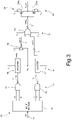
- In greater detail, and with reference to
Figure 3 , in a known embodiment, the row address signals ASr (for example, nine-bit digital signals) are received by theinput module 10 of therow decoder 5 and grouped appropriately into subsets in order to generate the grouped address signals PASLV, here designated by way of example as: px (referred to in what follows "as first address signals"), lx (referred to in what follows as "second address signals") and ly (referred to in what follows as "third address signals"). - For instance, considering a row address signal ASr<8:16>, the first address signals px may correspond to the three bits ASr<8:10>, the second address signals ly may correspond to the two bits ASr<11:12>, and the third address signals lx may correspond to the remaining four bits ASr<13:16>.
- The
input stage 10 further generates, based on the row address signals ASr, fourth address signals Is. - For instance, the fourth address signals ls may indicate the sector of the
memory array 2 that is to be selected, the first address signals px may indicate a block (in the example, of eight wordlines WL) to be addressed within the sector, and the second and third address signals lx and ly may indicate the specific wordlines WL to be addressed within the selected block. - The
pre-decoding module 12 comprises a plurality offirst logic gates 24, of a two-input, one-output NAND type, each of which receives at the inputs a respective first address signal px and a respective fourth address signal ls and supplies at the output a respective first low-voltage pre-decoded address signal, here designated by psx. - In the example described, the
first logic gates 24 are eight in number (i.e., in a number equal to the number of combinations that may be obtained starting from the address signals received at the input). - The
pre-decoding module 12 further comprises a plurality ofsecond logic gates 25, of a three-input, one-output NAND type, each of which receives at the inputs a respective second address signal lx, a respective third address signal ly, and a respective fourth address signal Is, and supplies at the output a second low-voltage pre-decoded address signal, here designated by sxy. - In the example described, the
second logic gates 25 are sixty-four in number (i.e., once again in a number equal to the number of combinations that may be obtained starting from the address signals received at the input). - The
first transport bus 13 comprises in this case eight lines for the first low-voltage pre-decoded address signals psx, and sixty-four lines for the second low-voltage pre-decoded address signals sxy, which are received at the input of thebooster module 14. - The
booster module 14 comprises a plurality offirst booster stages 26, each having an input that receives a respective first low-voltage pre-decoded address signal psx and an output that supplies a respective first pre-decoded address signal psxhv, having a high voltage; in the example, thefirst booster stages 26 are in a number equal to eight. - The
booster module 14 further comprises a plurality ofsecond booster stages 27, each having an input that receives a respective second low-voltage pre-decoded address signal sxy and an output that supplies a respective second pre-decoded address signal sxyhv, having a high voltage; in the example, thesecond booster stages 27 are sixty-four in number. - The
decoding module 16 comprises a plurality ofbuffer stages 28, operating as inverters, each receiving a first pre-decoded address signal psxhv and supplying at output, on thesecond transport bus 15, the negated version of the first pre-decoded address signal, designated by psxhvn. For instance, in the embodiment illustrated, a hundred and twenty-eightbuffer stages 28 are present (which appropriately enable an increase of the fan-out at output from the first booster stages 26). - The
decoding module 16 further comprises a plurality of logic-combination stages 29, each having: a first input that receives a respective first negated pre-decoded address signal psxhvn from arespective buffer stage 28; a second input that receives a respective second pre-decoded address signal sxyhv from a respectivesecond booster stage 27; and an output that supplies a respective decoded address signal DASHV. - Each logic-
combination stage 29 implements an OR logic operation between the pre-decoded address signals to be combined received at the input: psxhvn and sxyhv. - The decoded address signal DASHV thus has: a high value (high voltage) when any one, or both, of the pre-decoded address signals to be combined, psxhvn and sxyhv, have a high value; and a low value (ground, GND) when both of the pre-decoded address signals to be combined, psxhvn and sxyhv, have a low value.
- In the embodiment illustrated, the logic-
combination stages 29 are five hundred and twelve in number, i.e., equal to the number of wordlines WL to be addressed (and to the total number of combinations between the pre-decoded address signals to be combined psxhvn and sxyhv). - The
driving module 18 of therow decoder 5 comprises in this embodiment a plurality ofinverters 30, each having an input that receives a respective decoded address signal DASHV and an output that supplies the corresponding biasing signal S_WL for the respective wordlines WL of thememory array 2. The number ofinverters 30 is equal to the number of the wordlines WL to be addressed, in the example, five hundred and twelve. - In detail, each
inverter 30 comprises: afirst output transistor 31a, of a NMOS type, having its control terminal that receives the respective decoded address signal DASHV, its drain terminal that is connected to a respective wordline WL and on which the corresponding biasing signal S WL is present, and its source terminal that receives a reference voltage Vref, which may possibly have a negative value (or be equal to the ground reference GND); and asecond output transistor 31b, of a PMOS type, having its gate terminal that receives the respective decoded address signal DASHV, its drain terminal that is connected to the respective wordline WL and on which the corresponding biasing signal S_WL is present, and its source terminal that receives a boosted voltage, here designated by Vx, for example equal to the high voltage of 4.5 V. - To a low value of the decoded address signal DASHV corresponds a high output of the
inverter 30, with the corresponding biasing signal S_WL equal to the boosted voltage Vx; instead, to a high value of the decoded address signal DASHV corresponds a low output of theinverter 30, with the corresponding biasing signal S_WL equal to the reference voltage Vref. - A more detailed description is now made, with reference to
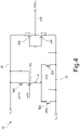
Figure 4 , of a known circuit embodiment of a logic-combination stage 29 of a standard CMOS type. - The logic-
combination stage 29 comprises six MOS transistors, namely: a first pair of input transistors, of a NMOS type, connected in parallel, and a second pair of input transistors, of a PMOS type, connected in series, which are designed to jointly implement the operation of OR logic combination of the pre-decoded address signals to be combined psxhvn and sxyhv received at the input; and a pair of output transistors, designed to supply on an output out the decoded address signal DASHV according to the result of the aforesaid OR logic combination. - In particular, in the first pair of input transistors, a
first NMOS transistor 32a is connected between afirst reference line 33, set at a first reference potential, for example equal to the reference voltage Vref, and aninternal node 34, and receives on a respective control terminal a respective first negated pre-decoded address signal psxhvn, and asecond NMOS transistor 32b is connected between thefirst reference line 33 and theinternal node 34, and receives on the respective control terminal a respective second pre-decoded address signal sxyhv. - In the second pair of input transistors, a
first PMOS transistor 32c and asecond PMOS transistor 32d are connected in series between theinternal node 34 and asecond reference line 35, set at a second reference potential, for example equal to the boosted voltage Vx, and receive on a respective control terminal the second pre-decoded address signal sxyhv and the first negated pre-decoded address signal psxhvn, respectively. - In the pair of output transistors, a pull-
up PMOS transistor 32e is connected between thesecond reference line 35 and the output out, and has its control terminal connected to theinternal node 34, and a pull-down PMOS transistor 32f is connected between thefirst reference line 33 and the same output out, and has its control terminal that is also connected to theinternal node 34. - It is evident that the logic-
combination stage 29 implements the following truth table in the OR logic combination of the pre-decoded address signals to be combined sxyhv and psxhvn:sxyhv psxhvn DAS HV 1 1 1 1 0 1 0 1 1 0 0 0 - In particular, when at least one of the pre-decoded address signals to be combined sxyhv and psxhvn has a high value, or when both of the pre-decoded address signals to be combined sxyhv and psxhvn have a high value, the
internal node 34 is set at the reference potential (given the closed state of one or both of theNMOS transistors up PMOS transistor 32e is closed, and the output out goes to the high value (boosted voltage Vx). - When, instead, both of the pre-decoded address signals to be combined sxyhv and psxhvn have a low value, the
internal node 34 is set at the high value (boosted voltage Vx), given the closed state of both of thePMOS transistors PMOS transistor 32f is closed and the output out goes to the low value (reference voltage Vref). - The present Applicant has realized that the row-decoding solution described previously has some limitations, in particular associated to a high occupation of area, which may prove important in applications where size reduction is required (for example, in portable applications).
-
US 6,111,792 A discloses a non-volatile semiconductor memory device comprising a mode signal output means for outputting a mode signal for conducting flash programming or flash erasing, a group selection signal output means for outputting a group selection signal for selecting a row decoding group, a first selection means for selecting the row decoding group controlling the word line in accordance with the group selection signal, and a second selection means selecting the word line corresponding to the memory cell from a plurality of the word lines controlled by the row decoding group selected by the first selection means. The time required for the flash programming and the flash erasing can be reduced without the addition of a further element and the chip areas can be reduced. - The aim of the present invention is to overcome, at least in part, the problem highlighted previously in order to provide a row-decoding solution that will be more compact and will have a smaller area occupation.
- According to the present invention, a row decoder and a corresponding non-volatile memory device are provided, as defined in the annexed claims.
- For a better understanding of the present invention, preferred embodiments thereof are now described purely by way of non-limiting example, with reference to the attached drawings, wherein:
-
Figure 1 shows a general block diagram of a non-volatile memory device of a known type; -
Figure 2 shows a general block diagram of a row decoder in the memory device ofFigure 1 , which is also of a known type; -
Figure 3 shows a more detailed block diagram of the row decoder ofFigure 2 ; -
Figure 4 shows a circuit diagram of a logic-combination stage in the row decoder ofFigure 3 ; -
Figure 5a shows a block diagram of a row decoder according to a first embodiment of the present solution; -
Figure 6a shows a circuit diagram of a logic-combination stage in the row decoder ofFigure 5a ; -
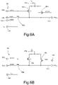
Figure 5b shows a block diagram of a row decoder according to a second embodiment of the present solution; -
Figure 6b shows a circuit diagram of a logic-combination stage in the row decoder ofFigure 5b ; -
Figure 5c shows a block diagram of a row decoder according to a third embodiment of the present solution; -
Figure 6c shows a circuit diagram of a logic-combination stage in the row decoder ofFigure 5c ; -
Figure 5d shows a block diagram of a row decoder according to a fourth embodiment of the present solution; and -
Figure 6d shows a circuit diagram of a logic-combination stage in the row decoder ofFigure 5d . - The present Applicant has realized that the decoding module and the corresponding plurality of logic-combination stages, one for each wordline WL to be addressed (see the foregoing discussion and
Figures 3 and4 ) represent an important contribution to the total area occupation of the row decoder. - One aspect of the present solution thus envisages a dedicated implementation (a so-called "custom" implementation) for the logic-combination stages of the decoding module, aimed at reducing area occupation of the row decoder.
- In particular, each logic-combination stage is designed for generating the decoded address signals DASHV by implementing the same operation of logic combination of the pre-decoded address signals as that of the known embodiment discussed with reference to
Figure 3 (so as not to require further circuit modifications), i.e., the logic OR between the first negated predecoded address signals psxhvn and the second predecoded address signals sxyhv (note that the first negated predecoded address signals psxhvn and the second predecoded address signals sxyhv are referred to in what follows also as "first and second predecoded address signals to be combined psxhvn, sxyhv"):
DASHV = (psxhvn) OR (sxyhv). - Each logic-combination stage thus implements the truth table referred to above:
sxyhv psxhvn DAS HV1 1 1 1 0 1 0 1 1 0 0 0 - In particular, and as will be highlighted hereinafter, each of the logic-combination stages has three signal inputs, which are designed to receive: one between a first and a second predecoded address signal to be combined psxhvn, sxyhv, and its negated version; and the other between a first and a second predecoded address signal to be combined psxhvn, sxyhv, or its negated version.
- As will be described in greater detail hereinafter, the logic-combination stages are configured to have an occupation of area halved as compared to traditional solutions, comprising in fact three MOS transistors (as opposed to six of the traditional solutions), of which:
- at least one MOS transfer transistor (also referred to as "pass transistor"), having the function of selectively transferring onto the output out the value of one between a first and a second predecoded address signal to be combined psxhvn, sxyhv, in at least one operating condition; in particular, the MOS pass transistor is controlled by the negated version of the other between a first and a second predecoded address signal to be combined psxhvn, sxyhv; and
- at least one pull-up MOS transistor, which is controlled by the negated version of the other between a first and a second predecoded address signal to be combined psxhvn, sxyhv, and has the function of selectively bringing to the high state the output out, in at least one operating condition.
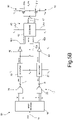
- In greater detail, and as illustrated in
Figure 5a (where elements that are similar to others already illustrated are designated by the same reference numbers and are not described again herein), in a first embodiment, the row decoder, here designated by 38, comprises, in a way substantially similar to what has been discussed previously: - the
input stage 10, which generates, based on the row address signals ASr, the address signals px, lx, ly and Is; - the
pre-decoding module 12, with the plurality of first logic gates 24 (in the example, eight in number), each of which receives at the inputs a respective first address signal px and a respective fourth address signal ls and supplies at the output a respective first low-voltage pre-decoded address signal psx; and the plurality of second logic gates 25 (in the example, sixty-four in number), each of which receives at the inputs a respective second address signal lx, a respective third address signal ly, and a respective fourth address signal Is, and supplies at the output a second low-voltage pre-decoded address signal sxy; - the
booster module 14, with the plurality of first booster stages 26 (in the example, eight in number), each having an input that receives a respective first low-voltage pre-decoded address signal psx and an output that supplies a respective first pre-decoded address signal psxhv; and the plurality of second booster stages 27 (in the example, sixty-four in number), each having an input that receives a respective second low-voltage pre-decoded address signal sxy and an output that supplies a respective second pre-decoded address signal sxyhv; and - the driving
module 18, with the plurality of inverters 30 (the number of the wordlines WL to be addressed, in the example, being five hundred and twelve), each having an input that receives a respective decoded address signal DASHV and an output that supplies the corresponding biasing signal S_WL for the respective wordlines WL of thememory array 2. - In the first embodiment, the decoding module, designated herein by 40, arranged between the
booster module 14 and the drivingmodule 18, comprises a plurality of logic-combination stages 42, each having: afirst input 42a that receives a respective first pre-decoded address signal psxhv from the first booster stages 26; asecond input 42b that receives a respective second pre-decoded address signal sxyhv from the second booster stages 27; athird input 42c that receives the second negated pre-decoded address signal sxyhvn (generated as discussed hereinafter); and an output out that supplies a respective decoded address signal DASHV. - It is emphasised once again that the negated version (psxhvn) of the first pre-decoded address signal psxhv constitutes the first predecoded address signal to be combined, and the second pre-decoded address signal sxyhv constitutes the second predecoded address signal to be combined by the logic-
combination stage 42. - Each logic-
combination stage 42 further has afourth input 42d, designed to receive the reference voltage Vref, and afifth input 42e designed to receive the boosted voltage Vx. - The
decoding module 40 comprises in this case a plurality of first buffer stages 44 (in the example, sixty-four in number) operating as inverters, each receiving a second pre-decoded address signal sxyhv from the second booster stages 27, and supplying at output the negated version of the same second pre-decoded address signal: sxyhvn. Instead, in this case no buffer stages at output from the first booster stages 26 are present. - With reference to
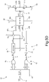
Figure 6a , a corresponding first embodiment is now described for the logic-combination stages 42, each comprising in this case: - a
single pass transistor 45a, of a NMOS type, which is connected between thesecond input 42b, on which it receives the second pre-decoded address signal sxyhv, and the output out, and has its control terminal that is connected to thefirst input 42a and receives the first pre-decoded address signal psxhv; and - a pair of pull-up PMOS transistors that are connected in parallel between the output out and the
fifth input 42e, the pair being formed by a first pull-uptransistor 46a, having its control terminal that is connected to thefirst input 42a and receives the first pre-decoded address signal psxhv, and by a second pull-uptransistor 46b, having its control terminal that is connected to thethird input 42c and receives the second negated pre-decoded address signal sxyhvn. - The bulk terminal of the
pass transistor 45a is biased at the reference voltage Vref (being coupled to thefourth input 42d), whereas the bulk terminal of the pull-uptransistors fifth input 42e). - The circuit configuration described enables implementation of the truth table discussed above, given that:
- when the first pre-decoded address signal to be combined psxhvn and the second pre-decoded address signal to be combined sxyhv are both high, the first and second pull-up
transistors - when the first pre-decoded address signal to be combined psxhvn has a low value and the second pre-decoded address signal to be combined sxyhv is high, the second pull-up
transistor 46b is closed, so as thepass transistor 45a, and the output out is again set at the high value; - in the case where the first pre-decoded address signal to be combined psxhvn is high and the second pre-decoded address signal to be combined sxyhv has a low value, the first pull-up
transistor 46a is closed and brings the output out to the high value; and - when both the first pre-decoded address signal to be combined psxhvn and the second pre-decoded address signal to be combined sxyhv have a low value, only the
pass transistor 45a is closed, thus bringing the output out to a low value. - It should further be noted that the circuit embodiment described is such as not to enable setting-up of a direct conduction path (which is potentially destructive) between the line set at the boosted voltage Vx and the line set at the reference potential Vref.
- With reference to
Figure 5b , a second embodiment of therow decoder 38 is now described, in which thedecoding module 40 further comprises a plurality of second buffer stages 46 (in the example, a hundred and twenty-eight), each receiving a first pre-decoded address signal psxhv from the first booster stages 26, and supplying at the output the negated version of the same first pre-decoded address signal, psxhvn. - Each logic-
combination stage 42 has in this case: afirst input 42a that receives a respective second negated pre-decoded address signal sxyhvn from the first buffer stages 44; asecond input 42b that receives a respective first negated pre-decoded address signal psxhvn from the second buffer stages 46; and athird input 42c that receives the respective first pre-decoded address signal psxhv from the first booster stages 26. - As illustrated in
Figure 6b , a corresponding second embodiment for the logic-combination stage 42 (which is, from the circuit standpoint, similar to the first embodiment) envisages in this case that: - the
single pass transistor 45a, of a NMOS type, receives from thesecond input 42b the first negated pre-decoded address signal psxhvn, and has a control terminal that receives the second negated pre-decoded address signal sxyhvn; and - the first pull-up
transistor 46a has a control terminal that receives the second negated pre-decoded address signal sxyhvn, and the second pull-uptransistor 46b has a control terminal that receives the first pre-decoded address signal psxhv. - It may be noted, in a way substantially similar to what has been discussed with reference to the first embodiment, that also this circuit configuration enables implementation of the desired truth table for the OR logic combination of the high predecoded address signals to be combined psxhvn, sxyhv, and in particular that:
- in the case where the first pre-decoded address signal to be combined psxhvn and the second pre-decoded address signal to be combined sxyhv are high, the first and second pull-up
transistors - when the first pre-decoded address signal to be combined psxhvn has a low value and the second pre-decoded address signal to be combined sxyhv is high, the first pull-up
transistor 46a is closed and the output out is at the high value; - in the case where the first pre-decoded address signal to be combined psxhvn is high and the second pre-decoded address signal to be combined sxyhv has a low value, both the
pass transistor 45a and the second pull-uptransistor 46b are closed, so that the output out is at the high value; and - when both the first pre-decoded address signal to be combined psxhvn and the second pre-decoded address signal to be combined sxyhv have a low value, the
single pass transistor 45a is closed, thus bringing the output out to the low value. - With reference to
Figure 5c , a third embodiment of therow decoder 38 is now described, in which thedecoding module 40 again comprises both the first and the second buffer stages 44, 46. - Each logic-
combination stage 42 has in this case: afirst input 42a that receives a respective second negated pre-decoded address signal sxyhvn from the first buffer stages 44; asecond input 42b that receives a first negated pre-decoded address signal psxhvn from the second buffer stages 46; and athird input 42c that receives the respective second pre-decoded address signal sxyhv from the second booster stages 27. - As illustrated in
Figure 6c , the logic-combination stage 42 in a corresponding third embodiment comprises: - a pair of pass transistors, connected between the
second input 42b and the output out, and in particular afirst pass transistor 45a, of a NMOS type, which has its control terminal that is connected to thefirst input 42a and receives the second negated pre-decoded address signal sxyhvn, and asecond pass transistor 45b, of a PMOS type, having its control terminal that is connected to thethird input 42c and receiving the second pre-decoded address signal sxyhv; and - a single pull-up
transistor 46a, of a PMOS type, connected between the output out and thefifth input 42e, having its control terminal that is connected to thefirst input 42a and receives the second negated pre-decoded address signal sxyhvn. - Also for this third embodiment, it may be noted that it implements the truth table of the operation of OR logic combination of the pre-decoded address signals to be combined psxhvn and sxyhv, and in particular that:
- when the first pre-decoded address signal to be combined psxhvn and the second pre-decoded address signal to be combined sxyhv are both high, the pull-up
transistor 46a is closed, and the output out is at the high value; - when the first pre-decoded address signal to be combined psxhvn has a low value and the second pre-decoded address signal to be combined sxyhv is high, again the pull-up
transistor 46a is closed and the output out is at the high value; - in the case where the first pre-decoded address signal to be combined psxhvn is high and the second pre-decoded address signal to be combined sxyhv has a low value, the first and
second pass transistors - when both the first pre-decoded address signal to be combined psxhvn and the second pre-decoded address signal to be combined sxyhv have a low value, the first and
second pass transistors - With reference first to
Figure 5d a fourth embodiment of the present solution is now discussed, in which thedecoding module 40 only comprises the second buffer stages 46 (the first buffer stages 44 in this case are not present) . - Each logic-
combination stage 42 has in this case: afirst input 42a that receives a respective first pre-decoded address signal psxhv from the first booster stages 26; asecond input 42b that receives a respective second pre-decoded address signal sxyhv from the second booster stages 27; and athird input 42c that receives the respective first negated pre-decoded address signal psxhvn from the second buffer stages 46. - As illustrated in
Figure 6d , a corresponding fourth embodiment of the logic-combination stage 42 is substantially similar to the third embodiment illustrated with reference toFigure 6c , and thus comprises: - the pair of pass transistors, connected between the
second input 42b, on which the second pre-decoded address signal sxyhv is present and the output out, with thefirst pass transistor 45a having its control terminal that is connected to thefirst input 42a and receiving the first pre-decoded address signal psxhv, and thesecond pass transistor 45b having its control terminal that is connected to thethird input 42c and receiving the first negated pre-decoded address signal psxhvn; and - the single pull-up
transistor 46a having its control terminal that is connected to thefirst input 42a and receiving the first pre-decoded address signal psxhv. - Also for this fourth embodiment, the truth table of the same operation of OR logic combination of the pre-decoded address signals to be combined psxhvn and sxyhv is implemented, given that:
- when the first pre-decoded address signal to be combined psxhvn and the second pre-decoded address signal to be combined sxyhv are both high, the pull-up
transistor 46a is closed, and the output out is at the high value; - when the first pre-decoded address signal to be combined psxhvn has a low value and the second pre-decoded address signal to be combined sxyhv is high, the first and
second pass transistors - in the case where the first pre-decoded address signal to be combined psxhvn is high and the second pre-decoded address signal to be combined sxyhv has a low value, the pull-up
transistor 46a is again closed, bringing the output out to the high value; and - when both the first pre-decoded address signal to be combined psxhvn and the second pre-decoded address signal to be combined sxyhv have a low value, the first and
second pass transistors - The advantages of the row decoder are clear from the foregoing description.
- In any case, it is emphasised once again that the solution proposed enables reduction of the occupation of area of the
row decoder 38 in a non-volatile memory device, in particular of a flash type. - This reduction of area occupation is principally afforded by the substantial halving of the dimensions of the logic-combination stages 42 in the final part of the
same row decoder 38. - In particular, the present Applicant has realized that, given the same performance as compared to known solutions (for example, the solution described with reference to
Figures 2 and3 ), it is possible to obtain a reduction of area of around 20% for theentire row decoder 38. - It is to be noted that removal of the
first buffer stage 44 or thesecond buffer stage 46 may contribute to the total reduction of area, at least in some embodiments; this removal may be accompanied, however, by an increase in the area of the first or second booster stages 26, 27 (in particular, of the corresponding output portion, principally for reasons of fan-out, as will be evident to a person skilled in the field). - The present Applicant further has realized that, given the same area as compared to traditional embodiments, the present solution alternatively enables an increase to be obtained in the speed of the decoding operations performed by the
row decoder 38 of around 30% of the total decoding time. - The aforesaid increase in speed may be achieved principally via increase of the area of the transistors of the
inverters 30 in thedriving module 18 of the row decoder 38 (this increase in turn being allowed by the aforementioned reduction of the area of the logic-combination stages 42). - Finally, it is clear that modifications and variations may be made to what has been described and illustrated herein, without thereby departing from the scope of the present invention, as defined in the annexed claims.
- In particular, it is evident that, depending on the dimensions of the memory array 2 (and the corresponding division into sectors), a different number of wordlines WL to be addressed may be provided, and, consequently, a different number of pre-decoding and coding signals.
- Furthermore, it is emphasised once again that the solution described may be applied in a wide range of non-volatile memory devices (for example, embedded or stand-alone flash devices), where a reduced occupation of area is required.
Claims (8)
- A row decoder (38), for a non-volatile memory device (1) provided with a memory array (2) having memory cells (3) arranged in a plurality of wordlines (WL), comprising:an input and pre-decoding module (10, 12, 14), configured to receive address signals (ASr) and generate pre-decoded address signals (PASHV);a decoding module (40), configured to receive said pre-decoded address signals (PASHV), to generate decoded address signals (DASHV), having a high or low value according to the decoding operation; anda driving module (18), configured to generate biasing signals (S_WL) for biasing of the wordlines (WL) of said memory array (2) starting from said decoded address signals (DASHV),characterized in that said decoding module (40) includes a plurality of decoding stages (42), each of which is designed to carry out an operation of OR logic combination between a first predecoded address signal (psxhvn) and a second predecoded address signal (sxyhv) to be combined to generate a respective decoded address signal (DASHV) on a respective output (out), and each of which comprises only three transistors, which include:- at least one first pass transistor (45a), designed to transfer selectively onto the output (out) the value of one between the first and second predecoded address signals to be combined (psxhvn, sxyhv), in at least one first operating condition;- at least one first pull-up transistor (46a), designed to selectively bring the output (out) to the high state, in at least one second operating condition; and- a second pull-up transistor (46b) operatively coupled to the first pull-up transistor (46a),wherein each decoding stage (42) has a first input (42a) designed to receive said negated version of the other between the first and second predecoded address signals to be combined (psxhvn, sxyhv), and a second input (42b), designed to receive said one between the first and second predecoded address signals to be combined (psxhvn, sxyhv);wherein said first pass transistor (45a) is connected between the second input (45b) and the output (out) and has its control terminal coupled to said first input (42a); said first pull-up transistor (46a) is connected between said output (out) and a further input (42e) set at a boosted voltage (Vx) and has its control terminal coupled to said first input (42a), said first pass transistor (45a) and said first pull-up transistor (46a) being controlled by the negated version of the other between the first and second predecoded address signals to be combined (psxhvn, sxyhv); and said second pull-up transistor (46b) is connected in parallel to said first pull-up transistor (46a) between said output (out) and said further input (42e) and has its control terminal that is coupled to a third input (42c) of said decoding stage (42) designed to receive the negated version of the one between the first and second predecoded address signals to be combined (psxhvn, sxyhv).
- A row decoder (38), for a non-volatile memory device (1) provided with a memory array (2) having memory cells (3) arranged in a plurality of wordlines (WL), comprising:an input and pre-decoding module (10, 12, 14), configured to receive address signals (ASr) and generate pre- decoded address signals (PASHV);a decoding module (40), configured to receive said pre- decoded address signals (PASHV), to generate decoded address signals (DASHV), having a high or low value according to the decoding operation; anda driving module (18), configured to generate biasing signals (S_WL) for biasing of the wordlines (WL) of said memory array (2) starting from said decoded address signals (DASHV),characterized in that said decoding module (40) includes a plurality of decoding stages (42), each of which is designed to carry out an operation of OR logic combination between a first predecoded address signal (psxhvn) and a second predecoded address signal (sxyhv) to be combined to generate a respective decoded address signal (DASHV)on a respective output (out), and each of which comprises only three transistors, which include:- at least one first pass transistor (45a), designed to transfer selectively onto the output (out) the value of one between the first and second predecoded address signals to be combined (psxhvn, sxyhv), in at least one first operating condition;- at least one first pull-up transistor (46a), designed to selectively bring the output (out) to the high state, in at least one second operating condition; and- a second pass transistor (45b) coupled to the first pass transistor (45a),wherein each decoding stage (42) has a first input (42a) designed to receive said negated version of the other between the first and second predecoded address signals to be combined (psxhvn, sxyhv), and a second input (42b), designed to receive said one between the first and second predecoded address signals to be combined (psxhvn, sxyhv);wherein said first pass transistor (45a) is connected between the second input (45b) and the output (out) and has its control terminal coupled to said first input (42a); said first pull-up transistor (46a) is connected between said output (out) and a further input (42e) set at a boosted voltage (Vx) and has its control terminal coupled to said first input (42a), said first pass transistor (45a) and said first pull-up transistor (46a) being controlled by the negated version of the other between the first and second predecoded address signals to be combined (psxhvn, sxyhv); and said second pass transistor (45b) is connected in parallel to said first pass transistor (45a) between said second input (45b) and said output (out) and has its control terminal that is coupled to a third input (42c) of said decoding stage (42) designed to receive the other between the first and second predecoded address signals to be combined (psxhvn, sxyhv).
- The decoder according to claim 1 or 2, wherein said first pass transistor (45a) is of a NMOS type, and said first pull-up transistor (46a) is of a PMOS type.
- The decoder according to any one of the preceding claims, wherein said decoding module (40) is configured to receive from said input and pre-decoding module (10, 12, 14) the negated version of the first predecoded address signals to be combined (psxhv), and the second predecoded address signals to be combined (sxyhv), and further comprises first buffer stages (44) and/or second buffer stages (46), which are designed to invert said second predecoded address signals to be combined (sxyhv) and/or said negated version of the first predecoded address signals to be combined (psxhv) and have outputs coupled to said decoding stages (42).
- The decoder according to any one of the preceding claims, wherein said input and pre-decoding module (10, 12, 14) comprises:an input module (10), configured to receive the address signals (ASr) and group together said address signals (ASr) into subsets for generating grouped address signals (PASLV);a pre-decoding module (12), configured to receive the grouped address signals (PASLV) and logically combine said grouped address signals (PASLV) for generating low-voltage pre-decoded address signals (
PAS LV); anda booster module (14), configured to receive said low-voltage pre-decoded address signals (PAS LV) and carry out a voltage-boosting operation for generation of said pre-decoded address signals (PASHV). - The decoder according to any one of the preceding claims, wherein said driving module (18) comprises a plurality of inverter units (30), one for each of said wordlines (WL); wherein each of said inverter units (30) is configured to receive a respective decoded address signal (DASHV)and supply a respective biasing signal (S_WL) for the respective wordline (WL) of the memory array (2).
- A non-volatile memory device (1), comprising a memory array (2), and a row decoder (20) according to any one of the preceding claims, coupled to the memory array (2) and designed to address and bias wordlines (WL) of said memory array.
- The device according to claim 7, wherein said memory array (2) is of a NAND or NOR flash type.
Applications Claiming Priority (1)
| Application Number | Priority Date | Filing Date | Title |
|---|---|---|---|
| ITUB2015A003728A ITUB20153728A1 (en) | 2015-09-18 | 2015-09-18 | ROW DECODER FOR A NON-VOLATILE MEMORY DEVICE, HAVING REDUCED AREA EMPLOYMENT |
Publications (2)
| Publication Number | Publication Date |
|---|---|
| EP3144937A1 EP3144937A1 (en) | 2017-03-22 |
| EP3144937B1 true EP3144937B1 (en) | 2022-05-04 |
Family
ID=55588163
Family Applications (1)
| Application Number | Title | Priority Date | Filing Date |
|---|---|---|---|
| EP16161883.0A Active EP3144937B1 (en) | 2015-09-18 | 2016-03-23 | Row decoder for a non-volatile memory device, having reduced area occupation |
Country Status (3)
| Country | Link |
|---|---|
| US (1) | US9767907B2 (en) |
| EP (1) | EP3144937B1 (en) |
| IT (1) | ITUB20153728A1 (en) |
Families Citing this family (3)
| Publication number | Priority date | Publication date | Assignee | Title |
|---|---|---|---|---|
| IT201600098496A1 (en) | 2016-09-30 | 2018-03-30 | St Microelectronics Srl | ADDRESS DECODER FOR A NON-VOLATILE MEMORY MATRIX USING SELECTION MOS TRANSISTORS |
| KR20190070158A (en) * | 2017-12-12 | 2019-06-20 | 에스케이하이닉스 주식회사 | Address decoder and semiconductor memory device including the same |
| KR102526256B1 (en) * | 2018-03-06 | 2023-04-28 | 에스케이하이닉스 주식회사 | Data output buffer |
Family Cites Families (7)
| Publication number | Priority date | Publication date | Assignee | Title |
|---|---|---|---|---|
| US5410508A (en) * | 1993-05-14 | 1995-04-25 | Micron Semiconductor, Inc. | Pumped wordlines |
| JP3227698B2 (en) * | 1998-03-16 | 2001-11-12 | 日本電気株式会社 | Nonvolatile semiconductor memory device |
| US7286439B2 (en) * | 2004-12-30 | 2007-10-23 | Sandisk 3D Llc | Apparatus and method for hierarchical decoding of dense memory arrays using multiple levels of multiple-headed decoders |
| JP5100035B2 (en) * | 2005-08-02 | 2012-12-19 | ルネサスエレクトロニクス株式会社 | Semiconductor memory device |
| ITTO20080645A1 (en) * | 2008-08-29 | 2010-02-28 | St Microelectronics Srl | ROW DECODER FOR NON-VOLATILE MEMORY DEVICES, IN PARTICULAR OF THE PHASE CHANGE TYPE |
| US8351264B2 (en) * | 2008-12-19 | 2013-01-08 | Unity Semiconductor Corporation | High voltage switching circuitry for a cross-point array |
| ITTO20120412A1 (en) * | 2012-05-08 | 2013-11-09 | St Microelectronics Srl | ROW DECODER CIRCUIT FOR A NON-VOLATILE MEMORY DEVICE WITH PHASE CHANGE |
-
2015
- 2015-09-18 IT ITUB2015A003728A patent/ITUB20153728A1/en unknown
-
2016
- 2016-03-23 EP EP16161883.0A patent/EP3144937B1/en active Active
- 2016-03-28 US US15/083,056 patent/US9767907B2/en active Active
Also Published As
| Publication number | Publication date |
|---|---|
| US9767907B2 (en) | 2017-09-19 |
| ITUB20153728A1 (en) | 2017-03-18 |
| EP3144937A1 (en) | 2017-03-22 |
| US20170084334A1 (en) | 2017-03-23 |
Similar Documents
| Publication | Publication Date | Title |
|---|---|---|
| US6144582A (en) | Nonvolatile semiconductor memory device | |
| US6535430B2 (en) | Wordline decoder for flash memory | |
| JP5059199B2 (en) | CMOS decoding circuit | |
| CN108352179B (en) | SRAM architecture for leakage reduction | |
| US6552952B2 (en) | Column multiplexer for semiconductor memories | |
| US9966145B2 (en) | Row decoder for a non-volatile memory device, and non-volatile memory device | |
| US6069838A (en) | Semiconductor memory device having sub-word line driving circuit | |
| EP3144937B1 (en) | Row decoder for a non-volatile memory device, having reduced area occupation | |
| KR100274923B1 (en) | Logic semiconductor integrated circuit device having embedded dynamic random access memory | |
| TWI644316B (en) | Semiconductor memory device | |
| US10559350B2 (en) | Memory circuit and electronic device | |
| US6111792A (en) | Non-volatile semiconductor memory device for selective cell flash erasing/programming | |
| US10360333B1 (en) | Configuration memory circuit | |
| US7639557B1 (en) | Configurable random-access-memory circuitry | |
| CN107086052B (en) | Flash memory | |
| US20070195605A1 (en) | Row selector with reduced area occupation for semiconductor memory devices | |
| JPH06150670A (en) | Semiconductor memory device | |
| US7378879B1 (en) | Decoding systems and methods | |
| US5491658A (en) | Column decoder for virtual ground memory array | |
| KR100399975B1 (en) | A positive charge pumping voltage switching circuit and a row decoder circuit of a flash memory using the same | |
| KR102365003B1 (en) | Otp memory device | |
| CN117711462A (en) | Nonvolatile memory device and corresponding operating method | |
| US6847579B2 (en) | Semiconductor memory device | |
| US20170179948A1 (en) | Signal transfer circuit and circuit for generating hit signal including the same |
Legal Events
| Date | Code | Title | Description |
|---|---|---|---|
| PUAI | Public reference made under article 153(3) epc to a published international application that has entered the european phase |
Free format text: ORIGINAL CODE: 0009012 |
|
| STAA | Information on the status of an ep patent application or granted ep patent |
Free format text: STATUS: THE APPLICATION HAS BEEN PUBLISHED |
|
| AK | Designated contracting states |
Kind code of ref document: A1 Designated state(s): AL AT BE BG CH CY CZ DE DK EE ES FI FR GB GR HR HU IE IS IT LI LT LU LV MC MK MT NL NO PL PT RO RS SE SI SK SM TR |
|
| AX | Request for extension of the european patent |
Extension state: BA ME |
|
| STAA | Information on the status of an ep patent application or granted ep patent |
Free format text: STATUS: REQUEST FOR EXAMINATION WAS MADE |
|
| 17P | Request for examination filed |
Effective date: 20170920 |
|
| RBV | Designated contracting states (corrected) |
Designated state(s): AL AT BE BG CH CY CZ DE DK EE ES FI FR GB GR HR HU IE IS IT LI LT LU LV MC MK MT NL NO PL PT RO RS SE SI SK SM TR |
|
| STAA | Information on the status of an ep patent application or granted ep patent |
Free format text: STATUS: EXAMINATION IS IN PROGRESS |
|
| 17Q | First examination report despatched |
Effective date: 20200814 |
|
| STAA | Information on the status of an ep patent application or granted ep patent |
Free format text: STATUS: EXAMINATION IS IN PROGRESS |
|
| GRAP | Despatch of communication of intention to grant a patent |
Free format text: ORIGINAL CODE: EPIDOSNIGR1 |
|
| STAA | Information on the status of an ep patent application or granted ep patent |
Free format text: STATUS: GRANT OF PATENT IS INTENDED |
|
| GRAJ | Information related to disapproval of communication of intention to grant by the applicant or resumption of examination proceedings by the epo deleted |
Free format text: ORIGINAL CODE: EPIDOSDIGR1 |
|
| GRAP | Despatch of communication of intention to grant a patent |
Free format text: ORIGINAL CODE: EPIDOSNIGR1 |
|
| STAA | Information on the status of an ep patent application or granted ep patent |
Free format text: STATUS: GRANT OF PATENT IS INTENDED |
|
| INTG | Intention to grant announced |
Effective date: 20211012 |
|
| INTG | Intention to grant announced |
Effective date: 20211027 |
|
| GRAS | Grant fee paid |
Free format text: ORIGINAL CODE: EPIDOSNIGR3 |
|
| GRAA | (expected) grant |
Free format text: ORIGINAL CODE: 0009210 |
|
| STAA | Information on the status of an ep patent application or granted ep patent |
Free format text: STATUS: THE PATENT HAS BEEN GRANTED |
|
| RAP3 | Party data changed (applicant data changed or rights of an application transferred) |
Owner name: STMICROELECTRONICS S.R.L. |
|
| AK | Designated contracting states |
Kind code of ref document: B1 Designated state(s): AL AT BE BG CH CY CZ DE DK EE ES FI FR GB GR HR HU IE IS IT LI LT LU LV MC MK MT NL NO PL PT RO RS SE SI SK SM TR |
|
| REG | Reference to a national code |
Ref country code: GB Ref legal event code: FG4D |
|
| REG | Reference to a national code |
Ref country code: CH Ref legal event code: EP |
|
| REG | Reference to a national code |
Ref country code: AT Ref legal event code: REF Ref document number: 1489977 Country of ref document: AT Kind code of ref document: T Effective date: 20220515 |
|
| REG | Reference to a national code |
Ref country code: DE Ref legal event code: R096 Ref document number: 602016071666 Country of ref document: DE |
|
| REG | Reference to a national code |
Ref country code: IE Ref legal event code: FG4D |
|
| REG | Reference to a national code |
Ref country code: LT Ref legal event code: MG9D |
|
| REG | Reference to a national code |
Ref country code: NL Ref legal event code: MP Effective date: 20220504 |
|
| REG | Reference to a national code |
Ref country code: AT Ref legal event code: MK05 Ref document number: 1489977 Country of ref document: AT Kind code of ref document: T Effective date: 20220504 |
|
| PG25 | Lapsed in a contracting state [announced via postgrant information from national office to epo] |
Ref country code: SE Free format text: LAPSE BECAUSE OF FAILURE TO SUBMIT A TRANSLATION OF THE DESCRIPTION OR TO PAY THE FEE WITHIN THE PRESCRIBED TIME-LIMIT Effective date: 20220504 Ref country code: PT Free format text: LAPSE BECAUSE OF FAILURE TO SUBMIT A TRANSLATION OF THE DESCRIPTION OR TO PAY THE FEE WITHIN THE PRESCRIBED TIME-LIMIT Effective date: 20220905 Ref country code: NO Free format text: LAPSE BECAUSE OF FAILURE TO SUBMIT A TRANSLATION OF THE DESCRIPTION OR TO PAY THE FEE WITHIN THE PRESCRIBED TIME-LIMIT Effective date: 20220804 Ref country code: NL Free format text: LAPSE BECAUSE OF FAILURE TO SUBMIT A TRANSLATION OF THE DESCRIPTION OR TO PAY THE FEE WITHIN THE PRESCRIBED TIME-LIMIT Effective date: 20220504 Ref country code: LT Free format text: LAPSE BECAUSE OF FAILURE TO SUBMIT A TRANSLATION OF THE DESCRIPTION OR TO PAY THE FEE WITHIN THE PRESCRIBED TIME-LIMIT Effective date: 20220504 Ref country code: HR Free format text: LAPSE BECAUSE OF FAILURE TO SUBMIT A TRANSLATION OF THE DESCRIPTION OR TO PAY THE FEE WITHIN THE PRESCRIBED TIME-LIMIT Effective date: 20220504 Ref country code: GR Free format text: LAPSE BECAUSE OF FAILURE TO SUBMIT A TRANSLATION OF THE DESCRIPTION OR TO PAY THE FEE WITHIN THE PRESCRIBED TIME-LIMIT Effective date: 20220805 Ref country code: FI Free format text: LAPSE BECAUSE OF FAILURE TO SUBMIT A TRANSLATION OF THE DESCRIPTION OR TO PAY THE FEE WITHIN THE PRESCRIBED TIME-LIMIT Effective date: 20220504 Ref country code: ES Free format text: LAPSE BECAUSE OF FAILURE TO SUBMIT A TRANSLATION OF THE DESCRIPTION OR TO PAY THE FEE WITHIN THE PRESCRIBED TIME-LIMIT Effective date: 20220504 Ref country code: BG Free format text: LAPSE BECAUSE OF FAILURE TO SUBMIT A TRANSLATION OF THE DESCRIPTION OR TO PAY THE FEE WITHIN THE PRESCRIBED TIME-LIMIT Effective date: 20220804 Ref country code: AT Free format text: LAPSE BECAUSE OF FAILURE TO SUBMIT A TRANSLATION OF THE DESCRIPTION OR TO PAY THE FEE WITHIN THE PRESCRIBED TIME-LIMIT Effective date: 20220504 |
|
| PG25 | Lapsed in a contracting state [announced via postgrant information from national office to epo] |
Ref country code: RS Free format text: LAPSE BECAUSE OF FAILURE TO SUBMIT A TRANSLATION OF THE DESCRIPTION OR TO PAY THE FEE WITHIN THE PRESCRIBED TIME-LIMIT Effective date: 20220504 Ref country code: PL Free format text: LAPSE BECAUSE OF FAILURE TO SUBMIT A TRANSLATION OF THE DESCRIPTION OR TO PAY THE FEE WITHIN THE PRESCRIBED TIME-LIMIT Effective date: 20220504 Ref country code: LV Free format text: LAPSE BECAUSE OF FAILURE TO SUBMIT A TRANSLATION OF THE DESCRIPTION OR TO PAY THE FEE WITHIN THE PRESCRIBED TIME-LIMIT Effective date: 20220504 Ref country code: IS Free format text: LAPSE BECAUSE OF FAILURE TO SUBMIT A TRANSLATION OF THE DESCRIPTION OR TO PAY THE FEE WITHIN THE PRESCRIBED TIME-LIMIT Effective date: 20220904 |
|
| PG25 | Lapsed in a contracting state [announced via postgrant information from national office to epo] |
Ref country code: SM Free format text: LAPSE BECAUSE OF FAILURE TO SUBMIT A TRANSLATION OF THE DESCRIPTION OR TO PAY THE FEE WITHIN THE PRESCRIBED TIME-LIMIT Effective date: 20220504 Ref country code: SK Free format text: LAPSE BECAUSE OF FAILURE TO SUBMIT A TRANSLATION OF THE DESCRIPTION OR TO PAY THE FEE WITHIN THE PRESCRIBED TIME-LIMIT Effective date: 20220504 Ref country code: RO Free format text: LAPSE BECAUSE OF FAILURE TO SUBMIT A TRANSLATION OF THE DESCRIPTION OR TO PAY THE FEE WITHIN THE PRESCRIBED TIME-LIMIT Effective date: 20220504 Ref country code: EE Free format text: LAPSE BECAUSE OF FAILURE TO SUBMIT A TRANSLATION OF THE DESCRIPTION OR TO PAY THE FEE WITHIN THE PRESCRIBED TIME-LIMIT Effective date: 20220504 Ref country code: DK Free format text: LAPSE BECAUSE OF FAILURE TO SUBMIT A TRANSLATION OF THE DESCRIPTION OR TO PAY THE FEE WITHIN THE PRESCRIBED TIME-LIMIT Effective date: 20220504 Ref country code: CZ Free format text: LAPSE BECAUSE OF FAILURE TO SUBMIT A TRANSLATION OF THE DESCRIPTION OR TO PAY THE FEE WITHIN THE PRESCRIBED TIME-LIMIT Effective date: 20220504 |
|
| REG | Reference to a national code |
Ref country code: DE Ref legal event code: R097 Ref document number: 602016071666 Country of ref document: DE |
|
| PLBE | No opposition filed within time limit |
Free format text: ORIGINAL CODE: 0009261 |
|
| STAA | Information on the status of an ep patent application or granted ep patent |
Free format text: STATUS: NO OPPOSITION FILED WITHIN TIME LIMIT |
|
| PG25 | Lapsed in a contracting state [announced via postgrant information from national office to epo] |
Ref country code: AL Free format text: LAPSE BECAUSE OF FAILURE TO SUBMIT A TRANSLATION OF THE DESCRIPTION OR TO PAY THE FEE WITHIN THE PRESCRIBED TIME-LIMIT Effective date: 20220504 |
|
| 26N | No opposition filed |
Effective date: 20230207 |
|
| PG25 | Lapsed in a contracting state [announced via postgrant information from national office to epo] |
Ref country code: SI Free format text: LAPSE BECAUSE OF FAILURE TO SUBMIT A TRANSLATION OF THE DESCRIPTION OR TO PAY THE FEE WITHIN THE PRESCRIBED TIME-LIMIT Effective date: 20220504 |
|
| PG25 | Lapsed in a contracting state [announced via postgrant information from national office to epo] |
Ref country code: MC Free format text: LAPSE BECAUSE OF FAILURE TO SUBMIT A TRANSLATION OF THE DESCRIPTION OR TO PAY THE FEE WITHIN THE PRESCRIBED TIME-LIMIT Effective date: 20220504 |
|
| REG | Reference to a national code |
Ref country code: CH Ref legal event code: PL |
|
| GBPC | Gb: european patent ceased through non-payment of renewal fee |
Effective date: 20230323 |
|
| REG | Reference to a national code |
Ref country code: BE Ref legal event code: MM Effective date: 20230331 |
|
| PG25 | Lapsed in a contracting state [announced via postgrant information from national office to epo] |
Ref country code: LU Free format text: LAPSE BECAUSE OF NON-PAYMENT OF DUE FEES Effective date: 20230323 |
|
| REG | Reference to a national code |
Ref country code: IE Ref legal event code: MM4A |
|
| PG25 | Lapsed in a contracting state [announced via postgrant information from national office to epo] |
Ref country code: GB Free format text: LAPSE BECAUSE OF NON-PAYMENT OF DUE FEES Effective date: 20230323 |
|
| PG25 | Lapsed in a contracting state [announced via postgrant information from national office to epo] |
Ref country code: LI Free format text: LAPSE BECAUSE OF NON-PAYMENT OF DUE FEES Effective date: 20230331 Ref country code: IT Free format text: LAPSE BECAUSE OF FAILURE TO SUBMIT A TRANSLATION OF THE DESCRIPTION OR TO PAY THE FEE WITHIN THE PRESCRIBED TIME-LIMIT Effective date: 20220504 Ref country code: IE Free format text: LAPSE BECAUSE OF NON-PAYMENT OF DUE FEES Effective date: 20230323 Ref country code: GB Free format text: LAPSE BECAUSE OF NON-PAYMENT OF DUE FEES Effective date: 20230323 Ref country code: FR Free format text: LAPSE BECAUSE OF NON-PAYMENT OF DUE FEES Effective date: 20230331 Ref country code: CH Free format text: LAPSE BECAUSE OF NON-PAYMENT OF DUE FEES Effective date: 20230331 |
|
| PG25 | Lapsed in a contracting state [announced via postgrant information from national office to epo] |
Ref country code: BE Free format text: LAPSE BECAUSE OF NON-PAYMENT OF DUE FEES Effective date: 20230331 |
|
| PGFP | Annual fee paid to national office [announced via postgrant information from national office to epo] |
Ref country code: DE Payment date: 20240220 Year of fee payment: 9 |