EP3144287A1 - AIN SINTERED BODY, AlN SUBSTRATE, AND METHOD FOR MANUFACTURING AlN SUBSTRATE - Google Patents
AIN SINTERED BODY, AlN SUBSTRATE, AND METHOD FOR MANUFACTURING AlN SUBSTRATE Download PDFInfo
- Publication number
- EP3144287A1 EP3144287A1 EP15792229.5A EP15792229A EP3144287A1 EP 3144287 A1 EP3144287 A1 EP 3144287A1 EP 15792229 A EP15792229 A EP 15792229A EP 3144287 A1 EP3144287 A1 EP 3144287A1
- Authority
- EP
- European Patent Office
- Prior art keywords
- aln
- sintered compact
- powder
- grain boundary
- mass
- Prior art date
- Legal status (The legal status is an assumption and is not a legal conclusion. Google has not performed a legal analysis and makes no representation as to the accuracy of the status listed.)
- Granted
Links
- 239000000758 substrate Substances 0.000 title claims description 61
- 238000000034 method Methods 0.000 title claims description 16
- 238000004519 manufacturing process Methods 0.000 title description 14
- 239000013078 crystal Substances 0.000 claims abstract description 94
- 239000000843 powder Substances 0.000 claims description 56
- 230000003746 surface roughness Effects 0.000 claims description 44
- PLDDOISOJJCEMH-UHFFFAOYSA-N neodymium oxide Inorganic materials [O-2].[O-2].[O-2].[Nd+3].[Nd+3] PLDDOISOJJCEMH-UHFFFAOYSA-N 0.000 claims description 43
- 238000005245 sintering Methods 0.000 claims description 37
- 239000000654 additive Substances 0.000 claims description 23
- 230000000996 additive effect Effects 0.000 claims description 23
- 239000000203 mixture Substances 0.000 claims description 19
- 238000002156 mixing Methods 0.000 claims description 14
- 229910052779 Neodymium Inorganic materials 0.000 claims description 12
- 229910052769 Ytterbium Inorganic materials 0.000 claims description 12
- 238000005498 polishing Methods 0.000 claims description 12
- 238000010438 heat treatment Methods 0.000 claims description 10
- 239000007787 solid Substances 0.000 claims description 9
- FIXNOXLJNSSSLJ-UHFFFAOYSA-N ytterbium(III) oxide Inorganic materials O=[Yb]O[Yb]=O FIXNOXLJNSSSLJ-UHFFFAOYSA-N 0.000 claims 3
- PMHQVHHXPFUNSP-UHFFFAOYSA-M copper(1+);methylsulfanylmethane;bromide Chemical compound Br[Cu].CSC PMHQVHHXPFUNSP-UHFFFAOYSA-M 0.000 description 147
- 229910003454 ytterbium oxide Inorganic materials 0.000 description 36
- 239000011230 binding agent Substances 0.000 description 13
- 230000010355 oscillation Effects 0.000 description 12
- RUDFQVOCFDJEEF-UHFFFAOYSA-N yttrium(III) oxide Inorganic materials [O-2].[O-2].[O-2].[Y+3].[Y+3] RUDFQVOCFDJEEF-UHFFFAOYSA-N 0.000 description 12
- 238000002441 X-ray diffraction Methods 0.000 description 9
- 239000000463 material Substances 0.000 description 6
- 238000005259 measurement Methods 0.000 description 6
- 238000012546 transfer Methods 0.000 description 6
- LFQSCWFLJHTTHZ-UHFFFAOYSA-N Ethanol Chemical compound CCO LFQSCWFLJHTTHZ-UHFFFAOYSA-N 0.000 description 5
- 239000002002 slurry Substances 0.000 description 5
- PNEYBMLMFCGWSK-UHFFFAOYSA-N aluminium oxide Inorganic materials [O-2].[O-2].[O-2].[Al+3].[Al+3] PNEYBMLMFCGWSK-UHFFFAOYSA-N 0.000 description 4
- 229910052593 corundum Inorganic materials 0.000 description 4
- 229910001845 yogo sapphire Inorganic materials 0.000 description 4
- KFZMGEQAYNKOFK-UHFFFAOYSA-N Isopropanol Chemical compound CC(C)O KFZMGEQAYNKOFK-UHFFFAOYSA-N 0.000 description 3
- PXHVJJICTQNCMI-UHFFFAOYSA-N Nickel Chemical compound [Ni] PXHVJJICTQNCMI-UHFFFAOYSA-N 0.000 description 3
- 239000004372 Polyvinyl alcohol Substances 0.000 description 3
- 238000005238 degreasing Methods 0.000 description 3
- 238000001095 inductively coupled plasma mass spectrometry Methods 0.000 description 3
- 239000002245 particle Substances 0.000 description 3
- 229920002451 polyvinyl alcohol Polymers 0.000 description 3
- 239000002904 solvent Substances 0.000 description 3
- 238000007088 Archimedes method Methods 0.000 description 2
- XKRFYHLGVUSROY-UHFFFAOYSA-N Argon Chemical compound [Ar] XKRFYHLGVUSROY-UHFFFAOYSA-N 0.000 description 2
- IJGRMHOSHXDMSA-UHFFFAOYSA-N Atomic nitrogen Chemical compound N#N IJGRMHOSHXDMSA-UHFFFAOYSA-N 0.000 description 2
- LRHPLDYGYMQRHN-UHFFFAOYSA-N N-Butanol Chemical compound CCCCO LRHPLDYGYMQRHN-UHFFFAOYSA-N 0.000 description 2
- 229920005822 acrylic binder Polymers 0.000 description 2
- 238000004458 analytical method Methods 0.000 description 2
- 239000012298 atmosphere Substances 0.000 description 2
- 238000007542 hardness measurement Methods 0.000 description 2
- 239000012299 nitrogen atmosphere Substances 0.000 description 2
- 230000003287 optical effect Effects 0.000 description 2
- 239000004065 semiconductor Substances 0.000 description 2
- PIGFYZPCRLYGLF-UHFFFAOYSA-N Aluminum nitride Chemical compound [Al]#N PIGFYZPCRLYGLF-UHFFFAOYSA-N 0.000 description 1
- PZNSFCLAULLKQX-UHFFFAOYSA-N Boron nitride Chemical compound N#B PZNSFCLAULLKQX-UHFFFAOYSA-N 0.000 description 1
- OKTJSMMVPCPJKN-UHFFFAOYSA-N Carbon Chemical compound [C] OKTJSMMVPCPJKN-UHFFFAOYSA-N 0.000 description 1
- 229910052786 argon Inorganic materials 0.000 description 1
- QVGXLLKOCUKJST-UHFFFAOYSA-N atomic oxygen Chemical compound [O] QVGXLLKOCUKJST-UHFFFAOYSA-N 0.000 description 1
- 229910052799 carbon Inorganic materials 0.000 description 1
- 239000001913 cellulose Substances 0.000 description 1
- 229920002678 cellulose Polymers 0.000 description 1
- 239000003795 chemical substances by application Substances 0.000 description 1
- 150000001875 compounds Chemical class 0.000 description 1
- 230000003247 decreasing effect Effects 0.000 description 1
- 238000010586 diagram Methods 0.000 description 1
- 239000002270 dispersing agent Substances 0.000 description 1
- 238000007580 dry-mixing Methods 0.000 description 1
- 230000000694 effects Effects 0.000 description 1
- 238000001125 extrusion Methods 0.000 description 1
- 230000017525 heat dissipation Effects 0.000 description 1
- 230000001771 impaired effect Effects 0.000 description 1
- 238000007373 indentation Methods 0.000 description 1
- 238000001746 injection moulding Methods 0.000 description 1
- 239000007788 liquid Substances 0.000 description 1
- 238000013507 mapping Methods 0.000 description 1
- 238000012986 modification Methods 0.000 description 1
- 230000004048 modification Effects 0.000 description 1
- 229910052759 nickel Inorganic materials 0.000 description 1
- 229910052757 nitrogen Inorganic materials 0.000 description 1
- 239000003960 organic solvent Substances 0.000 description 1
- 230000001590 oxidative effect Effects 0.000 description 1
- 239000001301 oxygen Substances 0.000 description 1
- 229910052760 oxygen Inorganic materials 0.000 description 1
- UZLYXNNZYFBAQO-UHFFFAOYSA-N oxygen(2-);ytterbium(3+) Chemical compound [O-2].[O-2].[O-2].[Yb+3].[Yb+3] UZLYXNNZYFBAQO-UHFFFAOYSA-N 0.000 description 1
- 239000004014 plasticizer Substances 0.000 description 1
- 229920002037 poly(vinyl butyral) polymer Polymers 0.000 description 1
- 230000005855 radiation Effects 0.000 description 1
- 238000004439 roughness measurement Methods 0.000 description 1
- 238000000790 scattering method Methods 0.000 description 1
- 239000000243 solution Substances 0.000 description 1
- 239000007921 spray Substances 0.000 description 1
- 238000004544 sputter deposition Methods 0.000 description 1
- 239000000126 substance Substances 0.000 description 1
- 238000010345 tape casting Methods 0.000 description 1
- XLYOFNOQVPJJNP-UHFFFAOYSA-N water Substances O XLYOFNOQVPJJNP-UHFFFAOYSA-N 0.000 description 1
Images
Classifications
-
- C—CHEMISTRY; METALLURGY
- C09—DYES; PAINTS; POLISHES; NATURAL RESINS; ADHESIVES; COMPOSITIONS NOT OTHERWISE PROVIDED FOR; APPLICATIONS OF MATERIALS NOT OTHERWISE PROVIDED FOR
- C09K—MATERIALS FOR MISCELLANEOUS APPLICATIONS, NOT PROVIDED FOR ELSEWHERE
- C09K5/00—Heat-transfer, heat-exchange or heat-storage materials, e.g. refrigerants; Materials for the production of heat or cold by chemical reactions other than by combustion
- C09K5/08—Materials not undergoing a change of physical state when used
- C09K5/14—Solid materials, e.g. powdery or granular
-
- C—CHEMISTRY; METALLURGY
- C04—CEMENTS; CONCRETE; ARTIFICIAL STONE; CERAMICS; REFRACTORIES
- C04B—LIME, MAGNESIA; SLAG; CEMENTS; COMPOSITIONS THEREOF, e.g. MORTARS, CONCRETE OR LIKE BUILDING MATERIALS; ARTIFICIAL STONE; CERAMICS; REFRACTORIES; TREATMENT OF NATURAL STONE
- C04B35/00—Shaped ceramic products characterised by their composition; Ceramics compositions; Processing powders of inorganic compounds preparatory to the manufacturing of ceramic products
- C04B35/515—Shaped ceramic products characterised by their composition; Ceramics compositions; Processing powders of inorganic compounds preparatory to the manufacturing of ceramic products based on non-oxide ceramics
- C04B35/58—Shaped ceramic products characterised by their composition; Ceramics compositions; Processing powders of inorganic compounds preparatory to the manufacturing of ceramic products based on non-oxide ceramics based on borides, nitrides, i.e. nitrides, oxynitrides, carbonitrides or oxycarbonitrides or silicides
- C04B35/581—Shaped ceramic products characterised by their composition; Ceramics compositions; Processing powders of inorganic compounds preparatory to the manufacturing of ceramic products based on non-oxide ceramics based on borides, nitrides, i.e. nitrides, oxynitrides, carbonitrides or oxycarbonitrides or silicides based on aluminium nitride
-
- C—CHEMISTRY; METALLURGY
- C04—CEMENTS; CONCRETE; ARTIFICIAL STONE; CERAMICS; REFRACTORIES
- C04B—LIME, MAGNESIA; SLAG; CEMENTS; COMPOSITIONS THEREOF, e.g. MORTARS, CONCRETE OR LIKE BUILDING MATERIALS; ARTIFICIAL STONE; CERAMICS; REFRACTORIES; TREATMENT OF NATURAL STONE
- C04B35/00—Shaped ceramic products characterised by their composition; Ceramics compositions; Processing powders of inorganic compounds preparatory to the manufacturing of ceramic products
- C04B35/622—Forming processes; Processing powders of inorganic compounds preparatory to the manufacturing of ceramic products
- C04B35/626—Preparing or treating the powders individually or as batches ; preparing or treating macroscopic reinforcing agents for ceramic products, e.g. fibres; mechanical aspects section B
- C04B35/63—Preparing or treating the powders individually or as batches ; preparing or treating macroscopic reinforcing agents for ceramic products, e.g. fibres; mechanical aspects section B using additives specially adapted for forming the products, e.g.. binder binders
- C04B35/6303—Inorganic additives
-
- C—CHEMISTRY; METALLURGY
- C04—CEMENTS; CONCRETE; ARTIFICIAL STONE; CERAMICS; REFRACTORIES
- C04B—LIME, MAGNESIA; SLAG; CEMENTS; COMPOSITIONS THEREOF, e.g. MORTARS, CONCRETE OR LIKE BUILDING MATERIALS; ARTIFICIAL STONE; CERAMICS; REFRACTORIES; TREATMENT OF NATURAL STONE
- C04B35/00—Shaped ceramic products characterised by their composition; Ceramics compositions; Processing powders of inorganic compounds preparatory to the manufacturing of ceramic products
- C04B35/622—Forming processes; Processing powders of inorganic compounds preparatory to the manufacturing of ceramic products
- C04B35/64—Burning or sintering processes
-
- H—ELECTRICITY
- H01—ELECTRIC ELEMENTS
- H01S—DEVICES USING THE PROCESS OF LIGHT AMPLIFICATION BY STIMULATED EMISSION OF RADIATION [LASER] TO AMPLIFY OR GENERATE LIGHT; DEVICES USING STIMULATED EMISSION OF ELECTROMAGNETIC RADIATION IN WAVE RANGES OTHER THAN OPTICAL
- H01S5/00—Semiconductor lasers
- H01S5/02—Structural details or components not essential to laser action
- H01S5/0206—Substrates, e.g. growth, shape, material, removal or bonding
-
- H—ELECTRICITY
- H01—ELECTRIC ELEMENTS
- H01S—DEVICES USING THE PROCESS OF LIGHT AMPLIFICATION BY STIMULATED EMISSION OF RADIATION [LASER] TO AMPLIFY OR GENERATE LIGHT; DEVICES USING STIMULATED EMISSION OF ELECTROMAGNETIC RADIATION IN WAVE RANGES OTHER THAN OPTICAL
- H01S5/00—Semiconductor lasers
- H01S5/02—Structural details or components not essential to laser action
- H01S5/022—Mountings; Housings
- H01S5/02218—Material of the housings; Filling of the housings
-
- H—ELECTRICITY
- H01—ELECTRIC ELEMENTS
- H01S—DEVICES USING THE PROCESS OF LIGHT AMPLIFICATION BY STIMULATED EMISSION OF RADIATION [LASER] TO AMPLIFY OR GENERATE LIGHT; DEVICES USING STIMULATED EMISSION OF ELECTROMAGNETIC RADIATION IN WAVE RANGES OTHER THAN OPTICAL
- H01S5/00—Semiconductor lasers
- H01S5/02—Structural details or components not essential to laser action
- H01S5/024—Arrangements for thermal management
- H01S5/02476—Heat spreaders, i.e. improving heat flow between laser chip and heat dissipating elements
-
- C—CHEMISTRY; METALLURGY
- C04—CEMENTS; CONCRETE; ARTIFICIAL STONE; CERAMICS; REFRACTORIES
- C04B—LIME, MAGNESIA; SLAG; CEMENTS; COMPOSITIONS THEREOF, e.g. MORTARS, CONCRETE OR LIKE BUILDING MATERIALS; ARTIFICIAL STONE; CERAMICS; REFRACTORIES; TREATMENT OF NATURAL STONE
- C04B2235/00—Aspects relating to ceramic starting mixtures or sintered ceramic products
- C04B2235/02—Composition of constituents of the starting material or of secondary phases of the final product
- C04B2235/30—Constituents and secondary phases not being of a fibrous nature
- C04B2235/32—Metal oxides, mixed metal oxides, or oxide-forming salts thereof, e.g. carbonates, nitrates, (oxy)hydroxides, chlorides
- C04B2235/3217—Aluminum oxide or oxide forming salts thereof, e.g. bauxite, alpha-alumina
- C04B2235/3222—Aluminates other than alumino-silicates, e.g. spinel (MgAl2O4)
-
- C—CHEMISTRY; METALLURGY
- C04—CEMENTS; CONCRETE; ARTIFICIAL STONE; CERAMICS; REFRACTORIES
- C04B—LIME, MAGNESIA; SLAG; CEMENTS; COMPOSITIONS THEREOF, e.g. MORTARS, CONCRETE OR LIKE BUILDING MATERIALS; ARTIFICIAL STONE; CERAMICS; REFRACTORIES; TREATMENT OF NATURAL STONE
- C04B2235/00—Aspects relating to ceramic starting mixtures or sintered ceramic products
- C04B2235/02—Composition of constituents of the starting material or of secondary phases of the final product
- C04B2235/30—Constituents and secondary phases not being of a fibrous nature
- C04B2235/32—Metal oxides, mixed metal oxides, or oxide-forming salts thereof, e.g. carbonates, nitrates, (oxy)hydroxides, chlorides
- C04B2235/3224—Rare earth oxide or oxide forming salts thereof, e.g. scandium oxide
-
- C—CHEMISTRY; METALLURGY
- C04—CEMENTS; CONCRETE; ARTIFICIAL STONE; CERAMICS; REFRACTORIES
- C04B—LIME, MAGNESIA; SLAG; CEMENTS; COMPOSITIONS THEREOF, e.g. MORTARS, CONCRETE OR LIKE BUILDING MATERIALS; ARTIFICIAL STONE; CERAMICS; REFRACTORIES; TREATMENT OF NATURAL STONE
- C04B2235/00—Aspects relating to ceramic starting mixtures or sintered ceramic products
- C04B2235/02—Composition of constituents of the starting material or of secondary phases of the final product
- C04B2235/30—Constituents and secondary phases not being of a fibrous nature
- C04B2235/32—Metal oxides, mixed metal oxides, or oxide-forming salts thereof, e.g. carbonates, nitrates, (oxy)hydroxides, chlorides
- C04B2235/3231—Refractory metal oxides, their mixed metal oxides, or oxide-forming salts thereof
- C04B2235/3251—Niobium oxides, niobates, tantalum oxides, tantalates, or oxide-forming salts thereof
- C04B2235/3255—Niobates or tantalates, e.g. silver niobate
-
- C—CHEMISTRY; METALLURGY
- C04—CEMENTS; CONCRETE; ARTIFICIAL STONE; CERAMICS; REFRACTORIES
- C04B—LIME, MAGNESIA; SLAG; CEMENTS; COMPOSITIONS THEREOF, e.g. MORTARS, CONCRETE OR LIKE BUILDING MATERIALS; ARTIFICIAL STONE; CERAMICS; REFRACTORIES; TREATMENT OF NATURAL STONE
- C04B2235/00—Aspects relating to ceramic starting mixtures or sintered ceramic products
- C04B2235/02—Composition of constituents of the starting material or of secondary phases of the final product
- C04B2235/30—Constituents and secondary phases not being of a fibrous nature
- C04B2235/38—Non-oxide ceramic constituents or additives
- C04B2235/3852—Nitrides, e.g. oxynitrides, carbonitrides, oxycarbonitrides, lithium nitride, magnesium nitride
- C04B2235/3865—Aluminium nitrides
-
- C—CHEMISTRY; METALLURGY
- C04—CEMENTS; CONCRETE; ARTIFICIAL STONE; CERAMICS; REFRACTORIES
- C04B—LIME, MAGNESIA; SLAG; CEMENTS; COMPOSITIONS THEREOF, e.g. MORTARS, CONCRETE OR LIKE BUILDING MATERIALS; ARTIFICIAL STONE; CERAMICS; REFRACTORIES; TREATMENT OF NATURAL STONE
- C04B2235/00—Aspects relating to ceramic starting mixtures or sintered ceramic products
- C04B2235/60—Aspects relating to the preparation, properties or mechanical treatment of green bodies or pre-forms
- C04B2235/612—Machining
-
- C—CHEMISTRY; METALLURGY
- C04—CEMENTS; CONCRETE; ARTIFICIAL STONE; CERAMICS; REFRACTORIES
- C04B—LIME, MAGNESIA; SLAG; CEMENTS; COMPOSITIONS THEREOF, e.g. MORTARS, CONCRETE OR LIKE BUILDING MATERIALS; ARTIFICIAL STONE; CERAMICS; REFRACTORIES; TREATMENT OF NATURAL STONE
- C04B2235/00—Aspects relating to ceramic starting mixtures or sintered ceramic products
- C04B2235/70—Aspects relating to sintered or melt-casted ceramic products
- C04B2235/96—Properties of ceramic products, e.g. mechanical properties such as strength, toughness, wear resistance
- C04B2235/963—Surface properties, e.g. surface roughness
Definitions
- the present invention relates to an AlN sintered compact, an AlN substrate and a method of producing an AlN substrate.
- An AlN substrate composed of an aluminum nitride (AlN) sintered compact has a significantly high thermal conductivity, and accordingly, it is utilized as a substrate to mount thereon a semiconductor device required to provide heat dissipation in particular (e.g., a light emitting device such as a semiconductor laser).
- a semiconductor device e.g., a light emitting device such as a semiconductor laser.
- Japanese Patent Laying-Open No. 2001-348275 discloses an AlN substrate for mounting a laser diode thereon.
- Patent document 1 Japanese Patent Laying-Open No. 2001-348275
- patent document 1 describes that in an AlN sintered compact sintered using yttria (Y 2 O 3 ) as a sintering additive, the number of AlN crystal grains per unit area and the length of a grain boundary which surrounds them are defined to implement an AlN substrate having a surface roughness Ra of 0.05 ⁇ m or less.
- yttria Y 2 O 3
- an object of the disclosure is to provide an AlN sintered compact with small surface roughness and an AlN substrate which allows excellently efficient heat transfer.
- An AlN sintered compact according to one aspect of the present invention includes AlN crystal grains and a grain boundary phase, and the grain boundary phase is lower in Vickers hardness than the AlN crystal grains.
- An AlN substrate production method includes the steps of: mixing AlN powder and a sintering additive including Yb 2 O 3 powder and Nd 2 O 3 powder to obtain a mixture; compacting the mixture to obtain a compact; subjecting the compact to a heat treatment to obtain an AlN sintered compact; and polishing a surface of the AlN sintered compact to obtain a main surface having a surface roughness Ra of 0.015 ⁇ m or less, in the step of mixing, the mixture having a solid content such that, of the solid content, the Yb 2 O 3 powder and the Nd 2 O 3 powder in total occupy a proportion equal to or greater than 1 mass% and equal to or less than 5 mass%.
- an AlN sintered compact with small surface roughness and an AlN substrate which allows excellently efficient heat transfer can be provided.
- an AlN substrate having surface roughness Ra of 0.015 ⁇ m or less can be easily produced.
- a first embodiment is an AlN sintered compact.
- the AlN sintered compact of the present embodiment includes AlN crystal grains as a major component, and, furthermore, includes a grain boundary phase as a balance.
- the AlN sintered compact of the present embodiment has the grain boundary phase lower in Vickers hardness than the AlN crystal grains. This can prevent the grain boundary phase from projecting on a polished surface of the AlN sintered compact. That is, surface roughness Ra can be reduced.
- the Vickers hardness of the AlN crystal grain and that of the grain boundary phase can be measured using a micro Vickers hardness meter.
- the micro Vickers hardness meter is a measurement instrument such that while a sample is observed under a microscope, an indenter can be pushed into a microscopic site within an observation field of view to measure the microscopic site's Vickers hardness.
- One such micro Vickers hardness meter is a micro Vickers hardness testing machine (model "HM-124", manufactured by "Mitutoyo Corp.”) etc., for example.
- a measuring load of 1 gf is set in the present embodiment.
- the AlN sintered compact is observed under a microscope, an AlN crystal grain or a grain boundary phase is selected, the indenter is pushed in, and Vickers hardness (HV) is calculated from a surface area of an indentation.
- HV Vickers hardness
- measurement is performed more than once (for example, about 5 times) for each of the AlN crystal grain and the grain boundary phase, and the Vickers hardness of the AlN crystal grain and that of the grain boundary phase are each determined from an average value of a plurality of measurements.
- the Vickers hardness of the AlN crystal grain and that of the grain boundary phase are controllable by a sintering condition, the sintering additive's composition, etc.
- the Vickers hardness of the AlN crystal grain is about HV 500-600, for example.
- the Vickers hardness of the grain boundary phase is for example about HV 250-500, preferably about HV 250-400, more preferably about HV 250-300.
- AlN crystal grains comprise a major portion of the sintered compact's structure (generally equal to or greater than 90 volume%).
- the volume content of the AlN crystal grains in the AlN sintered compact is preferably equal to or greater than 93 volume% and equal to or less than 99.5 volume%, more preferably equal to or greater than 95 volume% and equal to or less than 99.5 volume%, particularly preferably equal to or greater than 96 volume% and equal to or less than 99.5 volume%, since when the volume content of the AlN crystal grains occupies the above range, high thermal conductivity is obtained.
- the volume content of the AlN crystal grains in the AlN sintered compact can be measured for example by the following method. Initially, a surface of the AlN sintered compact is mirror-polished and a backscattered electron image of the polished surface is obtained using a scanning electron microscope (SEM). At the time, desirably, the observation magnification is about 1000-3000 times for example, and adjusted to allow about 150 AlN crystal grains to be in an observation field of view. Then, the backscattered electron image (an image in the observation field of view) is binarized and an area occupied by the AlN crystal grains in the image in the observation field of view is measured. And by dividing the AlN crystal grains' occupied area by the area of the AlN sintered compact in the image in the observation field of view, the volume content of the AlN crystal grains can be obtained.
- SEM scanning electron microscope
- the AlN crystal grain has a grain size for example of about 1-10 ⁇ m, preferably about 1-5 ⁇ m.
- the grain size is obtained as follows: in the backscattered electron image of the structure of the sintered compact obtained in the above volume content measurement, a diameter of a circle circumscribing an AlN crystal grain (i.e., a circumscribed circle diameter) is measured and regarded as the grain size.
- the grain boundary phase is formed between an AlN crystal grain and an AlN crystal grain.
- the grain boundary phase normally comprises a component derived from a sintering additive.
- a sintering additive Yb 2 O 3 , Nd 2 O 3 , Al 2 O 3 , Y 2 O 3 , etc. can be indicated as an example.
- the grain boundary phase includes a Yb 2 O 3 crystal phase and an AlNdO 3 crystal phase, since a grain boundary phase which includes both of these two crystal phases easily have low Vickers hardness.
- a component derived from Y 2 O 3 is not included.
- a component derived from Y 2 O 3 there are a Y 4 Al 2 O 9 crystal phase, a YAlO 3 crystal phase, etc., for example, since a grain boundary phase including these components easily has high Vickers hardness and a smooth polished surface cannot be obtained.
- What crystal phase is included in the grain boundary phase can be identified by an XRD method. More specifically, a crystal phase can be identified by measuring the AlN sintered compact's XRD pattern (diffraction peak's position and intensity) and comparing it with an XRD pattern of a compound described on a JCPDS (Joint Committee on Powder Diffraction StandardS) card. Note that assistively, an elemental mapping by an Electron ProbeMicro Analyzer (EPMA) may be used together to confirm that each crystal phase component is detected in the grain boundary phase.
- EPMA Electron ProbeMicro Analyzer
- a proportion of a total of Yb and Nd to the AlN sintered compact is equal to or greater than 0.87 mass% and equal to or less than 4.35 mass%, since a grain boundary phase which has such a composition is easily polished and surface roughness Ra can be reduced.
- the content of each element can be measured by the Inductively Coupled Plasma-Mass Spectrometry (ICP-MS).
- the proportion of a total of Yb and Nd to the AlN sintered compact is more preferably equal to or greater than 1.21 mass% and equal to or less than 4.35 mass%, and particularly preferably equal to or greater than 1.21 mass% and equal to or less than 2.00 mass%, since this allows surface roughness Ra to be further reduced.
- the density of the AlN sintered compact can be measured by the Archimedes method. More specifically, from the mass of a sample (the AlN sintered compact) a mass when the sample is immersed in water is deducted to obtain the sample's volume, and the sample's mass is divided by the volume to calculate the density.
- the density of the AlN sintered compact is preferably equal to or greater than 3.0 g/cm 3 , more preferably equal to or greater than 3.2 g/cm 3 , and particularly preferably equal to or greater than 3.3 g/cm 3 , since higher density helps to manifest suitable thermal conductivity.
- the density of the AlN sintered compact is adjustable by the amount of a sintering additive added, the sintering temperature and the like for example.
- a second embodiment is an AlN substrate.
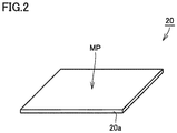
- the second embodiment provides an AlN substrate 20 including an AlN sintered compact 20a of the first embodiment, and having a main surface MP having surface roughness Ra of 0.015 ⁇ m or less.
- AlN substrate 20 is produced by polishing AlN sintered compact 20a of the first embodiment. Accordingly, it excellently efficiently transfers heat and it is suitable as a substrate for attaching a light emitting device.
- the shape of the substrate is not particularly limited and may be changed as appropriate depending on the application. For example, the shape can be rectangular or circular.
- Surface roughness Ra of main surface MP is 0.015 ⁇ m or less. This allows heat generated by a light emitting device to be efficiently transferred to AlN substrate 20 and can thus enhance the light emitting device's reliability.
- Surface roughness Ra can be measured with a general surface roughness meter.
- the surface roughness meter may be a contact type or may be a contactless type (an optical type).
- Surface roughness Ra is more preferably 0.012 ⁇ m or less, and particularly preferably 0.010 ⁇ m or less.
- Surface roughness Ra having a smaller value is more preferable, and ideally, it is zero, however, when productivity is considered, it is preferably 0.0005 ⁇ m or more.
- the thermal conductivity of AlN substrate 20 is measured in a laser flash method in conformity with "JIS R1611:2010."
- the laser flash method is a method such that a surface of a planar sample (for example, an AlN substrate) held at a constant temperature is irradiated with pulsed laser and thus heated instantaneously, and how the sample's back surface varies in temperature over time is measured to measure thermal diffusivity.
- thermal conductivity is calculable by multiplying the obtained thermal diffusivity by the sample's specific heat and density.
- AlN substrate 20 has thermal conductivity equal to or greater than 150 W/(m ⁇ K), since this allows heat transferred from a light emitting device to be rapidly removed. It is preferable that AlN substrate 20 have higher thermal conductivity. Accordingly, the thermal conductivity of AlN substrate 20 is more preferably equal to or greater than 160 W/(m ⁇ K), and particularly preferably equal to or greater than 170 W/(m ⁇ K). The upper limit value of the thermal conductivity is not particularly limited, however, when productivity is taken into consideration, the thermal conductivity is preferably equal to or less than 285 W/(m ⁇ K).
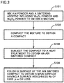
- FIG. 3 is a flowchart which outlines an AlN substrate production method according to the present embodiment.
- the production method of the present embodiment includes step S101, step S102, step S103, and step S104, and initially the AlN sintered compact of the first embodiment is produced (step S101 to step S103), and furthermore, the AlN sintered compact is polished to produce the AlN substrate (step S104).
- step S101 the AlN sintered compact of the first embodiment
- step S104 the AlN sintered compact is polished to produce the AlN substrate
- AlN powder and a sintering additive including Yb 2 O 3 powder and Nd 2 O 3 powder are mixed together to obtain a mixture.
- any other component may be added.
- a binder and a solvent as described later, and other than them, a dispersant, a plasticizer, a mold releasing agent, etc. can be indicated as an example.
- the mixing device can be a ball mill, an attritor, etc.
- the mixing may be dry mixing or wet mixing, however, when dispersibility is taken into consideration, wet mixing is preferable.
- wet mixing any solvent may be used.
- an organic solvent such as ethanol, isopropyl alcohol and butanol can be used.
- the mixing time is about 1-12 hours in general.
- the AlN powder preferably has an average particle size of about 0.1-5 ⁇ m, more preferably about 0.1-3 ⁇ m. Note that the average particle size indicates a value measured by a laser diffraction scattering method for the sake of illustration.
- Yb 2 O 3 powder and Nd 2 O 3 powder are used as a sintering additive, since by using these materials, a grain boundary phase of a low Vickers hardness is obtained. From a point of view of dispersibility, Yb 2 O 3 powder and Nd 2 O 3 powder preferably has an average particle size of about 0.1-5 ⁇ m, more preferably about 0.1-3 ⁇ m. Note that as the sintering additive, other than these, Al 2 O 3 powder etc. may for example be used.
- Yb 2 O 3 powder and Nd 2 O 3 powder are used in an amount set such that Yb 2 O 3 powder and Nd 2 O 3 powder in total occupy the mixture's solid content by 1 mass% or more and 5 mass% or less, since thereby a grain boundary phase including a Yb 2 O 3 crystal phase and an AlNdO 3 crystal phase is formed.
- Yb 2 O 3 powder and Nd 2 O 3 powder in total occupy the mixture's solid content preferably by 1.4 mass% or more and 5 mass% or less, particularly preferably by 1.4 mass% or more and 2.3 mass% or less to further ensure that a grain boundary phase including the Yb 2 O 3 crystal phase and the AlNdO 3 crystal phase is formed.
- the binder is not limited to any particular binder and a conventionally known material can be used.
- binders such as an acrylic binder, a polyvinyl alcohol (PVA) based binder, a polyvinyl butyral based binder, a cellulose based binder, etc. can be used. Two or more types of binders may be used together.
- the mixture (a slurry) is compacted to obtain a compact (a so-called "green sheet").
- a compact a so-called "green sheet”
- the compact can be obtained from the slurry by extrusion molding, injection molding, and tape casting (using a doctor blade etc.).
- the obtained compact may be air-dried or dried with hot air using a spray dryer etc.
- Step S103 the compact undergoes a heat treatment to provide an AlN sintered compact.
- Step S103 normally includes a degreasing step and a sintering step.
- a heat treatment is performed to remove an organic component of the binder etc.
- the heat treatment's temperature is about 500-900°C for example although it depends on the type of the binder used.
- the heat treatment's time is about 5-15 hours for example.
- the heat treatment's atmosphere is preferably a non-oxidizing atmosphere such as argon and nitrogen from a point of view to prevent oxygen from remaining.
- the degreased compact is sintered at 1780°C or more and 1900°C or less, since when the sintering temperature is less than 1780°C, insufficient sintering is provided and a dense sintered compact may not be obtained, which is unpreferable.
- the sintering temperature exceeds 1900°C coarse AlN crystal grains may be provided and the sintered compact's toughness etc. may be decreased, which is unpreferable.
- the sintering temperature is more preferably 1780°C or more 1850°C or less.
- the sintering may be done under the atmospheric pressure or while pressurized. Pressure applied when the sintering is done while pressurized is less than 10 atmospheres in general.
- a surface of AlN sintered compact 20a is polished to obtain main surface MP having surface roughness Ra of 0.015 ⁇ m or less.
- the polishing may be done in any method and for example it can be done by mechanical polishing using a loose abrasive or a bonded abrasive, chemical mechanical polishing using a polishing liquid, or the like.
- the AlN sintered compact of the present embodiment has a grain boundary phase softer than AlN crystal grains, and by polishing, surface roughness Ra can be 0.015 ⁇ m or less.
- step S101 to step S104 an AlN substrate having surface roughness Ra of 0.015 ⁇ m or less and excellently efficiently transferring heat can be produced.
- Sintered compacts No. 1A to No. 8A were produced under production conditions No. 1 to No. 8.
- AlN powder was prepared.
- Yb 2 O 3 powder, Nd 2 O 3 powder, Al 2 O 3 powder and Y 2 O 3 powder as a sintering additive, and an acrylic binder and a PVA based binder were prepared.
- AlN substrate (AlN sintered compact) production conditions amount of sintering additive blended sintering temperature Yb 2 O 3 powder Nd 2 O 3 powder Al 2 O 3 powder Y 2 O 3 powder total of Yb 2 O 3 powder & Nd 2 O 3 powder mass% mass% mass% mass% °C 1 1.3 1.0 0.9 0 2.3 1780 2 0.8 0.6 0.6 0 1.4 1850 3 2.8 2.2 1.8 0 5.0 1900 4 0.5 0.4 0.4 0 0.9 1880 5 3.5 3.0 2.7 0 6.5 1850 6 2.0 0 0.6 0 2.0 1850 7 0 2.5 1.8 0 2.5 1880 8 0 0 0 5 0 1850
- the slurry was supplied to an extruder. Inside the extruder, the slurry was kneaded and vacuum-degassed, and compressed and extruded through a die to provide a sheet-like compact (of 1.0 mm in thickness) (step S102).
- the compact After the compact was air-dried, the compact underwent a heat treatment in an nitrogen atmosphere at a temperature of 700°C for 10 hours to remove an organic component. A degreased product is thus obtained.
- the degreased product was disposed on a jig made of boron nitride (BN), and, together with the jig, disposed in a carbon furnace. And the degreased product underwent a heat treatment in a nitrogen atmosphere at sintering temperatures indicated in table 1 for 15 hours to obtain sintered compacts No. 1A to No. 8A (step S103).
- Sintered compacts No. 1A to No. 8A correspond to production conditions No. 1 to No. 8, respectively.
- the AlN sintered compact's density was measured by the Archimedes method, as has been set forth above. The result is shown in table 2.
- sintered compacts No. 1A to No. 5A correspond to working examples of the AlN sintered compact.
- the AlN sintered compact's crystal analysis was conducted using an X-ray diffractometer.
- the characteristic X-ray was a CuK ⁇ ray, and an angle of diffraction 2 ⁇ and diffraction intensity were measured.
- the XRD pattern was compared with JCPD card data to identify a crystal phase included in a grain boundary phase.
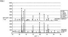
- the XRD patterns of sintered compacts No. 1A and No. 8A are indicated in Fig. 1 .
- Fig. 1 As shown in Fig. 1 , in sintered compact No. 1A using Yb 2 O 3 and Nd 2 O 3 as a sintering additive, a peak derived from a Yb 2 O 3 crystal phase and an AlNdO 3 crystal phase was observed.
- a micro Vickers hardness testing machine (a model "HM-124", manufactured by Mitutoyo Corp.) was used and a measuring load of 1 gf was applied to measure the Vickers hardness of an AlN crystal grain and that of a grain boundary phase in each sintered compact. The result is shown in table 2. Note that in table 2 the column “Vickers hardness” presents numerical values each indicating an average value in Vickers hardness of values obtained at five points of measurement.
- Sintered compacts No. 1A to No. 8A each had opposite main surfaces coarsely polished using a loose abrasive and subsequently had one main surface finely polished to obtain substrates No. 1B to No. 8B in the form of a rectangle having a length of 70 mm, a width of 70 mm, and a thickness of 0.25 mm. Substrates No. 1B to No. 8B correspond to sintered compacts No. 1A to No. 8A, respectively.
- Each substrate's surface roughness Ra was measured using a contactless type surface roughness measurement device (product name "NewView” produced by "ZYGO"). The result is indicated in table 2 and table 3.
- substrates No. 1B to No. 3B correspond to working examples of the AlN substrate.
- a thin nickel (Ni) film was formed on a main surface of each substrate.
- a laser diode (optical power: 200 mW, and oscillation wavelength: 1480 nm) was mounted thereon to produce a laser diode module.
- Each laser diode module was continuously operated and a percentage of an oscillation wavelength 1 hour after oscillation started divided by an oscillation wavelength when oscillation started was presented as laser oscillation's decrement rate. And laser oscillation's stability was assessed by two levels of "A” and "B” as indicated below. The result is shown in table 3.
- a sintered compact in which the Vickers hardness of the grain boundary phase is lower than the Vickers hardness of the AlN crystal grain has a tendency to have surface roughness Ra having a small value after it is polished than a sintered compact which does not satisfy such a condition.
- the sintered compact has low density, i.e., when the sintered compact has a density less than 3.2 g/cm 3 , it does not have a similar tendency. This is because it has a surface roughness increased by voids caused in the sintered compact when it has low density. Accordingly, the sintered compact's density is desirably equal to or greater than 3.2g/cm 3 .
- a sintered compact in which the Vickers hardness of the grain boundary phase is lower than the Vickers hardness of the AlN crystal grain has the grain boundary phase with the Yb 2 O 3 crystal phase and the AlNdO 3 crystal phase both included therein.
- a sintered compact in which the Vickers hardness of the grain boundary phase is higher than the Vickers hardness of the AlN crystal grain has the grain boundary phase with a component derived from either one of the Yb 2 O 3 crystal phase and the AlNdO 3 crystal phase or yttria included therein.
- the grain boundary phase includes both the Yb 2 O 3 crystal phase and the AlNdO 3 crystal phase.
- sintered compacts No. 1A to No. 3A containing Yb and Nd in a total amount equal to or greater than 0.87 mass% and equal to or less than 4.35 mass% allows surface roughness Ra to be reduced as compared with sintered compacts No. 4A and No. 5A which do not satisfy such a condition. Accordingly, it can be said that preferably, a proportion of a total amount of Yb and Nd to the AlN sintered compact is equal to or greater than 0.87 mass% and equal to or less than 4.35 mass%.
- step S101 in mixing the source materials (more specifically, in step S101), production conditions No. 1 to No. 3 in which, of the mixture's solid content, Yb 2 O 3 powder and Nd 2 O 3 powder in total occupy a proportion equal to or greater than 1 mass% and equal to or less than 5 mass%, allowed a sintered compact in which the Vickers hardness of the grain boundary phase is lower than the Vickers hardness of the AlN crystal grain, and furthermore, by polishing the sintered compact, an AlN substrate having surface roughness Ra of 0.015 ⁇ m or less was able to be produced.
Landscapes
- Chemical & Material Sciences (AREA)
- Engineering & Computer Science (AREA)
- Physics & Mathematics (AREA)
- Ceramic Engineering (AREA)
- Manufacturing & Machinery (AREA)
- Materials Engineering (AREA)
- Organic Chemistry (AREA)
- Structural Engineering (AREA)
- Condensed Matter Physics & Semiconductors (AREA)
- General Physics & Mathematics (AREA)
- Electromagnetism (AREA)
- Optics & Photonics (AREA)
- Inorganic Chemistry (AREA)
- Chemical Kinetics & Catalysis (AREA)
- Combustion & Propulsion (AREA)
- Thermal Sciences (AREA)
- Ceramic Products (AREA)
- Semiconductor Lasers (AREA)
Abstract
Description
- The present invention relates to an AlN sintered compact, an AlN substrate and a method of producing an AlN substrate.
- An AlN substrate composed of an aluminum nitride (AlN) sintered compact has a significantly high thermal conductivity, and accordingly, it is utilized as a substrate to mount thereon a semiconductor device required to provide heat dissipation in particular (e.g., a light emitting device such as a semiconductor laser). For example, Japanese Patent Laying-Open No.
2001-348275 - Patent document 1: Japanese Patent Laying-Open No.
2001-348275 - When using an AlN substrate as a substrate to mount a light emitting device thereon, it is important how smooth the substrate's surface is, since large surface roughness results in large thermal contact resistance and the light emitting device mounted on the substrate is impaired in reliability. More specifically, the heat which the light emitting device generates cannot be efficiently transferred to the AlN substrate, heat radiation is insufficient, and the light emitting device cannot stably oscillate and emit light.
- Conventionally a variety of proposals have been made in order to reduce an AlN substrate's surface roughness. For example, patent document 1 describes that in an AlN sintered compact sintered using yttria (Y2O3) as a sintering additive, the number of AlN crystal grains per unit area and the length of a grain boundary which surrounds them are defined to implement an AlN substrate having a surface roughness Ra of 0.05 µm or less.
- However, in recent years, as light emitting devices provide high outputs, a technique which can further efficiently transfer heat from a light emitting device to an AlN substrate, that is, further reduction of surface roughness, is demanded. Accordingly, the present inventors polished an AlN sintered compact sintered using yttria as a sintering additive to attempt to reduce its surface roughness, it has been found that such a sintered compact has some limit in surface roughness and it is difficult to provide efficient heat transfer beyond the status-quo.
- In view of the above problem, an object of the disclosure is to provide an AlN sintered compact with small surface roughness and an AlN substrate which allows excellently efficient heat transfer.
- An AlN sintered compact according to one aspect of the present invention includes AlN crystal grains and a grain boundary phase, and the grain boundary phase is lower in Vickers hardness than the AlN crystal grains.
- An AlN substrate production method according to one aspect of the present invention includes the steps of: mixing AlN powder and a sintering additive including Yb2O3 powder and Nd2O3 powder to obtain a mixture; compacting the mixture to obtain a compact; subjecting the compact to a heat treatment to obtain an AlN sintered compact; and polishing a surface of the AlN sintered compact to obtain a main surface having a surface roughness Ra of 0.015 µm or less, in the step of mixing, the mixture having a solid content such that, of the solid content, the Yb2O3 powder and the Nd2O3 powder in total occupy a proportion equal to or greater than 1 mass% and equal to or less than 5 mass%.
- According to the above, an AlN sintered compact with small surface roughness and an AlN substrate which allows excellently efficient heat transfer can be provided.
-
-
Fig. 1 is an XRD chart which shows an example of a diffraction pattern of an AlN sintered compact according to one aspect of the present invention. -
Fig. 2 is a schematic diagram showing an example of a configuration of an AlN substrate according to one aspect of the present invention. -
Fig. 3 is a flowchart which outlines a method of producing an AlN substrate according to one aspect of the present invention. - Initially, embodiments of the present invention will be enumerated and described.
- [1] An AlN sintered compact according to one aspect of the present invention includes AlN crystal grains and a grain boundary phase, and the grain boundary phase is lower in Vickers hardness than the AlN crystal grains.
In polishing an AlN sintered compact, there is a limit in surface roughness, which is attributed to the hardness of a grain boundary phase included in the sintered compact's structure. More specifically, it is believed that the grain boundary phase is harder than AlN crystal grains which occupy a major portion of the sintered compact's structure and is relatively hard to polish, and accordingly, on a polished surface the grain boundary phase remains in a projecting state and a smooth surface cannot be obtained. Accordingly, as described above, the grain boundary phase's Vickers hardness is restricted to be lower than the AlN crystal grain's Vickers hardness. This can prevent a polished surface form having a projecting grain boundary phase and reduce surface roughness.
Herein, in the AlN sintered compact, the "Vickers hardness" of the AlN crystal grain and that of the grain boundary phase can be measured for example with a micro Vickers hardness meter. - [2] Preferably, the grain boundary phase includes a Yb2O3 crystal phase and an AlNdO3 crystal phase.
Generally, an AlN sintered compact is produced by compacting a mixture including AlN powder, a sintering additive, etc. into a prescribed form, and sintering the mixture. The sintered compact thus obtained will have a grain boundary phase containing a component derived from the sintering additive. When yttria (Y2O3) is used as a sintering additive, the grain boundary phase will be composed of a Y4Al2O9 crystal phase, a YAlO3 crystal phase, etc., and would have Vickers hardness exceeding the AlN crystal grain's Vickers hardness.
On the other hand, when ytterbium oxide (Yb2O3) and neodymium oxide (Nd2O3) are used as a sintering additive, the grain boundary phase includes a Yb2O3 crystal phase and an AlNdO3 crystal phase, and its Vickers hardness is easily lower than the AlN crystal grain's Vickers hardness. Accordingly, by the grain boundary phase including the Yb2O3 crystal phase and the AlNdO3 crystal phase, further improved surface roughness can be achieved.
Note that what type of crystal phase is included in the grain boundary phase can be identified by subjecting the AlN sintered compact to X-ray diffraction (XRD). - [3] Preferably, the grain boundary phase includes Yb and Nd, and a proportion of a total of Yb and Nd to the AlN sintered compact is equal to or greater than 0.87 mass% and equal to or less than 4.35 mass%, since such a grain boundary phase has a low Vickers hardness.
- [4] The AlN sintered compact according to one aspect of the present invention includes the AlN sintered compact of any one of items [1] to [3] above and, at a surface of the AlN sintered compact, has a main surface having a surface roughness Ra of 0.015 µm or less.
The AlN sintered compact of any one of items [1] to [3] above has a grain boundary phase larger in hardness than the AlN crystal grain and can be polished to have surface roughness Ra of 0.015 µm or less. And the AlN substrate having surface roughness Ra of 0.015 µm or less has a low thermal contact resistance and excellently efficiently transfers heat.
Herein "surface roughness Ra" indicates "arithmetic mean roughness Ra" defined by "JIS B0601:2013" for the sake of illustration. - [5] Preferably, the AlN substrate has a thermal conductivity equal to or greater than 150 W/(m · K), since this can rapidly remove heat from a light emitting device and thus enhance the light emitting device in reliability.
- [6] A method of producing an AlN substrate according to one aspect of the present invention includes the steps of: mixing AlN powder and a sintering additive including Yb2O3 powder and Nd2O3 powder to obtain a mixture; compacting the mixture to obtain a compact; and subjecting the compact to a heat treatment to obtain an AlN sintered compact; and polishing a surface of the AlN sintered compact to obtain a main surface having a surface roughness Ra of 0.015 µm or less, in the step of mixing, the mixture having a solid content such that, of the solid content, the Yb2O3 powder and the Nd2O3 powder in total occupy a proportion equal to or greater than 1 mass% and equal to or less than 5 mass%.
- According to the production method, an AlN substrate having surface roughness Ra of 0.015 µm or less can be easily produced.
- The present invention will now be described in embodiments (hereinafter also referred to as "the present embodiment") hereinafter in detail, however, the present embodiments are not limited thereto.
- A first embodiment is an AlN sintered compact. The AlN sintered compact of the present embodiment includes AlN crystal grains as a major component, and, furthermore, includes a grain boundary phase as a balance.
- The AlN sintered compact of the present embodiment has the grain boundary phase lower in Vickers hardness than the AlN crystal grains. This can prevent the grain boundary phase from projecting on a polished surface of the AlN sintered compact. That is, surface roughness Ra can be reduced.
- The Vickers hardness of the AlN crystal grain and that of the grain boundary phase can be measured using a micro Vickers hardness meter. The micro Vickers hardness meter is a measurement instrument such that while a sample is observed under a microscope, an indenter can be pushed into a microscopic site within an observation field of view to measure the microscopic site's Vickers hardness. One such micro Vickers hardness meter is a micro Vickers hardness testing machine (model "HM-124", manufactured by "Mitutoyo Corp.") etc., for example.
- A measuring load of 1 gf is set in the present embodiment. And the AlN sintered compact is observed under a microscope, an AlN crystal grain or a grain boundary phase is selected, the indenter is pushed in, and Vickers hardness (HV) is calculated from a surface area of an indentation. Desirably, in order to increase measurement accuracy, measurement is performed more than once (for example, about 5 times) for each of the AlN crystal grain and the grain boundary phase, and the Vickers hardness of the AlN crystal grain and that of the grain boundary phase are each determined from an average value of a plurality of measurements.
- The Vickers hardness of the AlN crystal grain and that of the grain boundary phase are controllable by a sintering condition, the sintering additive's composition, etc. The Vickers hardness of the AlN crystal grain is about HV 500-600, for example. Furthermore, the Vickers hardness of the grain boundary phase is for example about HV 250-500, preferably about HV 250-400, more preferably about HV 250-300.
- AlN crystal grains comprise a major portion of the sintered compact's structure (generally equal to or greater than 90 volume%). The volume content of the AlN crystal grains in the AlN sintered compact is preferably equal to or greater than 93 volume% and equal to or less than 99.5 volume%, more preferably equal to or greater than 95 volume% and equal to or less than 99.5 volume%, particularly preferably equal to or greater than 96 volume% and equal to or less than 99.5 volume%, since when the volume content of the AlN crystal grains occupies the above range, high thermal conductivity is obtained.
- The volume content of the AlN crystal grains in the AlN sintered compact can be measured for example by the following method. Initially, a surface of the AlN sintered compact is mirror-polished and a backscattered electron image of the polished surface is obtained using a scanning electron microscope (SEM). At the time, desirably, the observation magnification is about 1000-3000 times for example, and adjusted to allow about 150 AlN crystal grains to be in an observation field of view. Then, the backscattered electron image (an image in the observation field of view) is binarized and an area occupied by the AlN crystal grains in the image in the observation field of view is measured. And by dividing the AlN crystal grains' occupied area by the area of the AlN sintered compact in the image in the observation field of view, the volume content of the AlN crystal grains can be obtained.
- Furthermore, from a point of view of the sintered compact's strength, the AlN crystal grain has a grain size for example of about 1-10 µm, preferably about 1-5 µm. Note that the grain size is obtained as follows: in the backscattered electron image of the structure of the sintered compact obtained in the above volume content measurement, a diameter of a circle circumscribing an AlN crystal grain (i.e., a circumscribed circle diameter) is measured and regarded as the grain size.
- The grain boundary phase is formed between an AlN crystal grain and an AlN crystal grain. The grain boundary phase normally comprises a component derived from a sintering additive. As the sintering additive, Yb2O3, Nd2O3, Al2O3, Y2O3, etc. can be indicated as an example.
- Preferably, the grain boundary phase includes a Yb2O3 crystal phase and an AlNdO3 crystal phase, since a grain boundary phase which includes both of these two crystal phases easily have low Vickers hardness. On the other hand, it is preferable that a component derived from Y2O3 is not included. As a component derived from Y2O3, there are a Y4Al2O9 crystal phase, a YAlO3 crystal phase, etc., for example, since a grain boundary phase including these components easily has high Vickers hardness and a smooth polished surface cannot be obtained.
- What crystal phase is included in the grain boundary phase can be identified by an XRD method. More specifically, a crystal phase can be identified by measuring the AlN sintered compact's XRD pattern (diffraction peak's position and intensity) and comparing it with an XRD pattern of a compound described on a JCPDS (Joint Committee on Powder Diffraction StandardS) card. Note that assistively, an elemental mapping by an Electron ProbeMicro Analyzer (EPMA) may be used together to confirm that each crystal phase component is detected in the grain boundary phase.
- Preferably, a proportion of a total of Yb and Nd to the AlN sintered compact is equal to or greater than 0.87 mass% and equal to or less than 4.35 mass%, since a grain boundary phase which has such a composition is easily polished and surface roughness Ra can be reduced. Note that the content of each element can be measured by the Inductively Coupled Plasma-Mass Spectrometry (ICP-MS). The proportion of a total of Yb and Nd to the AlN sintered compact is more preferably equal to or greater than 1.21 mass% and equal to or less than 4.35 mass%, and particularly preferably equal to or greater than 1.21 mass% and equal to or less than 2.00 mass%, since this allows surface roughness Ra to be further reduced.
- Furthermore, from a similar point of view, in the AlN sintered compact, the mass ratio of Yb and Nd is for example Yb:Nd = about 1:(0.75-0.79) and is preferably Yb:Nd = about 1: (0.75-0.77).
- The density of the AlN sintered compact can be measured by the Archimedes method. More specifically, from the mass of a sample (the AlN sintered compact) a mass when the sample is immersed in water is deducted to obtain the sample's volume, and the sample's mass is divided by the volume to calculate the density. The density of the AlN sintered compact is preferably equal to or greater than 3.0 g/cm3, more preferably equal to or greater than 3.2 g/cm3, and particularly preferably equal to or greater than 3.3 g/cm3, since higher density helps to manifest suitable thermal conductivity. The density of the AlN sintered compact is adjustable by the amount of a sintering additive added, the sintering temperature and the like for example.
- A second embodiment is an AlN substrate. With reference to
Fig. 2 , the second embodiment provides anAlN substrate 20 including an AlN sintered compact 20a of the first embodiment, and having a main surface MP having surface roughness Ra of 0.015 µm or less.AlN substrate 20 is produced by polishing AlN sintered compact 20a of the first embodiment. Accordingly, it excellently efficiently transfers heat and it is suitable as a substrate for attaching a light emitting device. The shape of the substrate is not particularly limited and may be changed as appropriate depending on the application. For example, the shape can be rectangular or circular. - Surface roughness Ra of main surface MP is 0.015 µm or less. This allows heat generated by a light emitting device to be efficiently transferred to
AlN substrate 20 and can thus enhance the light emitting device's reliability. Surface roughness Ra can be measured with a general surface roughness meter. The surface roughness meter may be a contact type or may be a contactless type (an optical type). Surface roughness Ra is more preferably 0.012 µm or less, and particularly preferably 0.010 µm or less. Surface roughness Ra having a smaller value is more preferable, and ideally, it is zero, however, when productivity is considered, it is preferably 0.0005 µm or more. - The thermal conductivity of
AlN substrate 20 is measured in a laser flash method in conformity with "JIS R1611:2010." The laser flash method is a method such that a surface of a planar sample (for example, an AlN substrate) held at a constant temperature is irradiated with pulsed laser and thus heated instantaneously, and how the sample's back surface varies in temperature over time is measured to measure thermal diffusivity. And thermal conductivity is calculable by multiplying the obtained thermal diffusivity by the sample's specific heat and density. - Preferably,
AlN substrate 20 has thermal conductivity equal to or greater than 150 W/(m · K), since this allows heat transferred from a light emitting device to be rapidly removed. It is preferable thatAlN substrate 20 have higher thermal conductivity. Accordingly, the thermal conductivity ofAlN substrate 20 is more preferably equal to or greater than 160 W/(m · K), and particularly preferably equal to or greater than 170 W/(m · K). The upper limit value of the thermal conductivity is not particularly limited, however, when productivity is taken into consideration, the thermal conductivity is preferably equal to or less than 285 W/(m · K). - An AlN substrate of the present embodiment can be produced in a method described hereinafter.
Fig. 3 is a flowchart which outlines an AlN substrate production method according to the present embodiment. As indicated inFig. 3 , the production method of the present embodiment includes step S101, step S102, step S103, and step S104, and initially the AlN sintered compact of the first embodiment is produced (step S101 to step S103), and furthermore, the AlN sintered compact is polished to produce the AlN substrate (step S104). Hereinafter, each step will be described. - At step S101, AlN powder and a sintering additive including Yb2O3 powder and Nd2O3 powder are mixed together to obtain a mixture.
- At step S101, as long as AlN powder and the sintering additive including Yb2O3 powder and Nd2O3 powder are used, any other component may be added. As any component, a binder and a solvent as described later, and other than them, a dispersant, a plasticizer, a mold releasing agent, etc. can be indicated as an example.
- The mixing device can be a ball mill, an attritor, etc. The mixing may be dry mixing or wet mixing, however, when dispersibility is taken into consideration, wet mixing is preferable. In the wet mixing, any solvent may be used. For example, an organic solvent such as ethanol, isopropyl alcohol and butanol can be used. The mixing time is about 1-12 hours in general.
- From a point of view of the density of the sintered compact, the AlN powder preferably has an average particle size of about 0.1-5 µm, more preferably about 0.1-3 µm. Note that the average particle size indicates a value measured by a laser diffraction scattering method for the sake of illustration.
- In the present embodiment, Yb2O3 powder and Nd2O3 powder are used as a sintering additive, since by using these materials, a grain boundary phase of a low Vickers hardness is obtained. From a point of view of dispersibility, Yb2O3 powder and Nd2O3 powder preferably has an average particle size of about 0.1-5 µm, more preferably about 0.1-3 µm. Note that as the sintering additive, other than these, Al2O3 powder etc. may for example be used.
- Yb2O3 powder and Nd2O3 powder are used in an amount set such that Yb2O3 powder and Nd2O3 powder in total occupy the mixture's solid content by 1 mass% or more and 5 mass% or less, since thereby a grain boundary phase including a Yb2O3 crystal phase and an AlNdO3 crystal phase is formed. Note that Yb2O3 powder and Nd2O3 powder in total occupy the mixture's solid content preferably by 1.4 mass% or more and 5 mass% or less, particularly preferably by 1.4 mass% or more and 2.3 mass% or less to further ensure that a grain boundary phase including the Yb2O3 crystal phase and the AlNdO3 crystal phase is formed.
- Furthermore, from a similar point of view, Yb2O3 powder and Nd2O3 powder are used in amounts, respectively, at a ratio (a mass ratio) for example of Yb2O3 powder:Nd2O3 powder = about 1:(0.75-0.79), preferably Yb2O3 powder:Nd2O3 powder = about 1:(0.75-0.77).
- The binder is not limited to any particular binder and a conventionally known material can be used. For example, binders such as an acrylic binder, a polyvinyl alcohol (PVA) based binder, a polyvinyl butyral based binder, a cellulose based binder, etc. can be used. Two or more types of binders may be used together.
- At
step 102, the mixture (a slurry) is compacted to obtain a compact (a so-called "green sheet"). This may be done in any method, and for example, the compact can be obtained from the slurry by extrusion molding, injection molding, and tape casting (using a doctor blade etc.). The obtained compact may be air-dried or dried with hot air using a spray dryer etc. - At step S103, the compact undergoes a heat treatment to provide an AlN sintered compact. Step S103 normally includes a degreasing step and a sintering step.
- In the degreasing step, a heat treatment is performed to remove an organic component of the binder etc. The heat treatment's temperature is about 500-900°C for example although it depends on the type of the binder used. The heat treatment's time is about 5-15 hours for example. The heat treatment's atmosphere is preferably a non-oxidizing atmosphere such as argon and nitrogen from a point of view to prevent oxygen from remaining.
- In the sintering step, the degreased compact is sintered at 1780°C or more and 1900°C or less, since when the sintering temperature is less than 1780°C, insufficient sintering is provided and a dense sintered compact may not be obtained, which is unpreferable. When the sintering temperature exceeds 1900°C coarse AlN crystal grains may be provided and the sintered compact's toughness etc. may be decreased, which is unpreferable. The sintering temperature is more preferably 1780°C or more 1850°C or less. The sintering may be done under the atmospheric pressure or while pressurized. Pressure applied when the sintering is done while pressurized is less than 10 atmospheres in general.
- At step S104, a surface of AlN sintered compact 20a is polished to obtain main surface MP having surface roughness Ra of 0.015 µm or less. The polishing may be done in any method and for example it can be done by mechanical polishing using a loose abrasive or a bonded abrasive, chemical mechanical polishing using a polishing liquid, or the like. As has been previously discussed, the AlN sintered compact of the present embodiment has a grain boundary phase softer than AlN crystal grains, and by polishing, surface roughness Ra can be 0.015 µm or less.
- Thus by performing step S101 to step S104, an AlN substrate having surface roughness Ra of 0.015 µm or less and excellently efficiently transferring heat can be produced.
- Hereinafter, although the present embodiment will more specifically be described using examples, the present embodiment is not limited to these examples.
- Sintered compacts No. 1A to No. 8A were produced under production conditions No. 1 to No. 8.
- AlN powder was prepared. Yb2O3 powder, Nd2O3 powder, Al2O3 powder and Y2O3 powder as a sintering additive, and an acrylic binder and a PVA based binder were prepared.
- The above source materials were blended as a binder (17 mass%), a sintering additive (components and amounts blended as indicated in table 1), and AlN powder (a balance), and furthermore, a solvent (ethanol) was added, and the materials were mixed together for 6 hours using a ball mill (step S101). Thus a mixture (a slurry) was obtained. In table 1, production conditions No. 1 to No. 3 correspond to working examples of the production method.
Table 1 production condition Nos. AlN substrate (AlN sintered compact) production conditions amount of sintering additive blended sintering temperature Yb2O3 powder Nd2O3 powder Al2O3 powder Y2O3 powder total of Yb2O3 powder & Nd2O3 powder mass% mass% mass% mass% mass% °C 1 1.3 1.0 0.9 0 2.3 1780 2 0.8 0.6 0.6 0 1.4 1850 3 2.8 2.2 1.8 0 5.0 1900 4 0.5 0.4 0.4 0 0.9 1880 5 3.5 3.0 2.7 0 6.5 1850 6 2.0 0 0.6 0 2.0 1850 7 0 2.5 1.8 0 2.5 1880 8 0 0 0 5 0 1850 - The slurry was supplied to an extruder. Inside the extruder, the slurry was kneaded and vacuum-degassed, and compressed and extruded through a die to provide a sheet-like compact (of 1.0 mm in thickness) (step S102).
- After the compact was air-dried, the compact underwent a heat treatment in an nitrogen atmosphere at a temperature of 700°C for 10 hours to remove an organic component. A degreased product is thus obtained.
- Then, the degreased product was disposed on a jig made of boron nitride (BN), and, together with the jig, disposed in a carbon furnace. And the degreased product underwent a heat treatment in a nitrogen atmosphere at sintering temperatures indicated in table 1 for 15 hours to obtain sintered compacts No. 1A to No. 8A (step S103). Sintered compacts No. 1A to No. 8A correspond to production conditions No. 1 to No. 8, respectively.
- The AlN sintered compact's density was measured by the Archimedes method, as has been set forth above. The result is shown in table 2. In table 2, sintered compacts No. 1A to No. 5A correspond to working examples of the AlN sintered compact.
Table 2 sintered compact Nos. AlN sintered compact density crystal phase detected via XRD element content Vickers hardness (HV) surface roughness Ra Yb Nd total of Yb & Nd AlN crystal grain grain boundary phase g/cm3 mass % mass % mass% µm 1A 3.30 Yb2O3 crystal phase 1.14 0.86 2.00 574 273 0.010 AlNdO3 crystal phase 2A 3.20 Yb2O3 crystal phase 0.70 0.51 1.21 540 280 0.010 AlNdO3 crystal phase 3A 3.33 Yb2O3 crystal phase 2.46 1.89 4.35 605 276 0.012 AlNdO3 crystal phase 4A 2.50 Yb2O3 crystal phase 0.44 0.34 0.78 581 282 1.0 AlNdO3 crystal phase 5A 3.38 Yb2O3 crystal phase 3.07 2.57 5.64 557 282 0.030 AlNdO3 crystal phase 6A 2.50 Yb2O3 crystal phase 1.76 0 1.76 591 656 1.6 7A 3.32 AlNdO3 crystal phase 0 2.15 2.15 591 713 0.040 8A 3.34 Y4Al2O9 crystal phase 0 0 0 541 824 0.027 YAlO3 crystal phase - The AlN sintered compact's crystal analysis was conducted using an X-ray diffractometer. The characteristic X-ray was a CuKα ray, and an angle of diffraction 2θ and diffraction intensity were measured. And the XRD pattern was compared with JCPD card data to identify a crystal phase included in a grain boundary phase. The XRD patterns of sintered compacts No. 1A and No. 8A are indicated in
Fig. 1 . As shown inFig. 1 , in sintered compact No. 1A using Yb2O3 and Nd2O3 as a sintering additive, a peak derived from a Yb2O3 crystal phase and an AlNdO3 crystal phase was observed. On the other hand, in sintered compact No. 8A using Y2O3 as a sintering additive, a peak derived from these crystal phases was not observed, and a peak derived from a Y4Al2O9 crystal phase and a YAlO3 crystal phase was observed. Each sintered compact's analysis result is shown in table 2. - Each sintered compact's Yb and Nd contents were measured using an ICP-MS device. The result is shown in table 2.
- A micro Vickers hardness testing machine (a model "HM-124", manufactured by Mitutoyo Corp.) was used and a measuring load of 1 gf was applied to measure the Vickers hardness of an AlN crystal grain and that of a grain boundary phase in each sintered compact. The result is shown in table 2. Note that in table 2 the column "Vickers hardness" presents numerical values each indicating an average value in Vickers hardness of values obtained at five points of measurement.
- Sintered compacts No. 1A to No. 8A each had opposite main surfaces coarsely polished using a loose abrasive and subsequently had one main surface finely polished to obtain substrates No. 1B to No. 8B in the form of a rectangle having a length of 70 mm, a width of 70 mm, and a thickness of 0.25 mm. Substrates No. 1B to No. 8B correspond to sintered compacts No. 1A to No. 8A, respectively.
- Each substrate's surface roughness Ra was measured using a contactless type surface roughness measurement device (product name "NewView" produced by "ZYGO"). The result is indicated in table 2 and table 3. In table 3, substrates No. 1B to No. 3B correspond to working examples of the AlN substrate.
Table 3 substrate Nos. AlN substrate thermal conductivity surface roughness Ra stability of laser oscillation W/(m · K) µm 1B 180 0.010 A 2B 160 0.010 A 3B 170 0.012 A 4B 90 1.5 B 5B 170 0.030 B 6B 104 1.1 B 7B 141 0.040 B 8B 179 0.027 B - As has been discussed above, a laser flash method was used to each substrate's thermal conductivity. The result is shown in table 3.
- By sputtering, a thin nickel (Ni) film was formed on a main surface of each substrate. And a laser diode (optical power: 200 mW, and oscillation wavelength: 1480 nm) was mounted thereon to produce a laser diode module.
- Each laser diode module was continuously operated and a percentage of an oscillation wavelength 1 hour after oscillation started divided by an oscillation wavelength when oscillation started was presented as laser oscillation's decrement rate. And laser oscillation's stability was assessed by two levels of "A" and "B" as indicated below. The result is shown in table 3.
- A: laser oscillation' decrement rate is less than 8%.
- B: laser oscillation' decrement rate is 15% or more.
- From table 2, a sintered compact in which the Vickers hardness of the grain boundary phase is lower than the Vickers hardness of the AlN crystal grain has a tendency to have surface roughness Ra having a small value after it is polished than a sintered compact which does not satisfy such a condition.
- However, when the sintered compact has low density, i.e., when the sintered compact has a density less than 3.2 g/cm3, it does not have a similar tendency. This is because it has a surface roughness increased by voids caused in the sintered compact when it has low density. Accordingly, the sintered compact's density is desirably equal to or greater than 3.2g/cm3.
- Furthermore, from table 2, it can be seen that a sintered compact in which the Vickers hardness of the grain boundary phase is lower than the Vickers hardness of the AlN crystal grain (i.e., No. 1A to No. 5A) has the grain boundary phase with the Yb2O3 crystal phase and the AlNdO3 crystal phase both included therein. In contrast, a sintered compact in which the Vickers hardness of the grain boundary phase is higher than the Vickers hardness of the AlN crystal grain (i.e., No. 6A to No. 8A) has the grain boundary phase with a component derived from either one of the Yb2O3 crystal phase and the AlNdO3 crystal phase or yttria included therein. Thus it can be said that preferably the grain boundary phase includes both the Yb2O3 crystal phase and the AlNdO3 crystal phase.
- Furthermore, from table 2, sintered compacts No. 1A to No. 3A containing Yb and Nd in a total amount equal to or greater than 0.87 mass% and equal to or less than 4.35 mass% allows surface roughness Ra to be reduced as compared with sintered compacts No. 4A and No. 5A which do not satisfy such a condition. Accordingly, it can be said that preferably, a proportion of a total amount of Yb and Nd to the AlN sintered compact is equal to or greater than 0.87 mass% and equal to or less than 4.35 mass%.
- From table 3, it has been confirmed that laser diode modules using substrates No. 1B to No. 3B having surface roughness Ra of 0.015 µm or less present stable laser oscillation. This is because it is believed that thermal contact resistance became small as surface roughness Ra is 0.015 µm or less.
- From tables 1-3, in mixing the source materials (more specifically, in step S101), production conditions No. 1 to No. 3 in which, of the mixture's solid content, Yb2O3 powder and Nd2O3 powder in total occupy a proportion equal to or greater than 1 mass% and equal to or less than 5 mass%, allowed a sintered compact in which the Vickers hardness of the grain boundary phase is lower than the Vickers hardness of the AlN crystal grain, and furthermore, by polishing the sintered compact, an AlN substrate having surface roughness Ra of 0.015 µm or less was able to be produced.
- Thus while the present embodiments and examples were described, it is also initially planned to combine the configuration of each embodiment and that of each example as appropriate.
- It should be understood that the embodiments and examples disclosed herein have been described for the purpose of illustration only and in a non-restrictive manner in any respect. The scope of the present invention is defined by the terms of the claims, rather than the embodiment described above, and is intended to include any modifications within the meaning and scope equivalent to the terms of the claims.
-
- 20: AlN substrate; 20a: AlN sintered compact; MP: main surface.
Claims (6)
- An AlN sintered compact comprising an AlN crystal grain and a grain boundary phase,
the grain boundary phase being lower in Vickers hardness than the AlN crystal grain. - The AlN sintered compact according to claim 1, wherein the grain boundary phase includes a Yb2O3 crystal phase and an AlNdO3 crystal phase.
- The AlN sintered compact according to claim 1 or 2, wherein:the grain boundary phase includes Yb and Nd; anda proportion of a total of Yb and Nd to the AlN sintered compact is equal to or greater than 0.87 mass% and equal to or less than 4.35 mass%.
- An AlN substrate comprising the AlN sintered compact according to any one of claims 1-3, and, at a surface of the AlN sintered compact, having a main surface having a surface roughness Ra of 0.015 µm or less.
- The AlN substrate according to claim 4, having a thermal conductivity equal to or greater than 150 W/(m · K).
- A method of producing an AlN substrate, the method comprising the steps of:mixing AlN powder and a sintering additive including Yb2O3 powder and Nd2O3 powder to obtain a mixture;compacting the mixture to obtain a compact;subjecting the compact to a heat treatment to obtain an AlN sintered compact; andpolishing a surface of the AlN sintered compact to obtain a main surface having a surface roughness Ra of 0.015 µm or less,in the step of mixing, the mixture having a solid content such that, of the solid content, the Yb2O3 powder and the Nd2O3 powder in total occupy a proportion equal to or greater than 1 mass% and equal to or less than 5 mass%.
Applications Claiming Priority (2)
| Application Number | Priority Date | Filing Date | Title |
|---|---|---|---|
| JP2014098505A JP6262598B2 (en) | 2014-05-12 | 2014-05-12 | AlN sintered body, AlN substrate, and manufacturing method of AlN substrate |
| PCT/JP2015/061415 WO2015174186A1 (en) | 2014-05-12 | 2015-04-14 | AIN SINTERED BODY, AlN SUBSTRATE, AND METHOD FOR MANUFACTURING AlN SUBSTRATE |
Publications (3)
| Publication Number | Publication Date |
|---|---|
| EP3144287A1 true EP3144287A1 (en) | 2017-03-22 |
| EP3144287A4 EP3144287A4 (en) | 2017-08-23 |
| EP3144287B1 EP3144287B1 (en) | 2019-08-07 |
Family
ID=54479730
Family Applications (1)
| Application Number | Title | Priority Date | Filing Date |
|---|---|---|---|
| EP15792229.5A Active EP3144287B1 (en) | 2014-05-12 | 2015-04-14 | Aln sintered compact, aln substrate and method of producing aln substrate |
Country Status (5)
| Country | Link |
|---|---|
| US (1) | US20170152425A1 (en) |
| EP (1) | EP3144287B1 (en) |
| JP (1) | JP6262598B2 (en) |
| KR (1) | KR20170007372A (en) |
| WO (1) | WO2015174186A1 (en) |
Families Citing this family (1)
| Publication number | Priority date | Publication date | Assignee | Title |
|---|---|---|---|---|
| JP6546538B2 (en) * | 2016-01-29 | 2019-07-17 | 日本特殊陶業株式会社 | Aluminum nitride sintered body and method of manufacturing the same |
Family Cites Families (8)
| Publication number | Priority date | Publication date | Assignee | Title |
|---|---|---|---|---|
| JP3633636B2 (en) * | 1993-02-05 | 2005-03-30 | 住友電気工業株式会社 | Aluminum nitride sintered body |
| JP4161423B2 (en) * | 1997-10-30 | 2008-10-08 | 住友電気工業株式会社 | Aluminum nitride sintered body and metallized substrate thereof |
| JPH11322432A (en) * | 1998-05-22 | 1999-11-24 | Sumitomo Electric Ind Ltd | Green body and sintered body of aln powder, and their production |
| JP2001064079A (en) * | 1999-08-25 | 2001-03-13 | Sumitomo Electric Ind Ltd | Aluminum nitride sintered body and method for producing the same |
| JP2001196152A (en) * | 2000-01-13 | 2001-07-19 | Sumitomo Electric Ind Ltd | Ceramic heater |
| JP4551536B2 (en) | 2000-06-02 | 2010-09-29 | 株式会社東芝 | AlN substrate and laser diode element using the same |
| JP5283420B2 (en) * | 2008-04-04 | 2013-09-04 | 株式会社トクヤマ | Aluminum nitride sintered body and manufacturing method thereof |
| KR101705024B1 (en) * | 2011-07-14 | 2017-02-09 | 가부시끼가이샤 아라이도 마테리아루 | Aln substrate and method for producing same |
-
2014
- 2014-05-12 JP JP2014098505A patent/JP6262598B2/en active Active
-
2015
- 2015-04-14 EP EP15792229.5A patent/EP3144287B1/en active Active
- 2015-04-14 WO PCT/JP2015/061415 patent/WO2015174186A1/en not_active Ceased
- 2015-04-14 US US15/310,181 patent/US20170152425A1/en not_active Abandoned
- 2015-04-14 KR KR1020167034514A patent/KR20170007372A/en not_active Withdrawn
Also Published As
| Publication number | Publication date |
|---|---|
| JP6262598B2 (en) | 2018-01-17 |
| EP3144287B1 (en) | 2019-08-07 |
| KR20170007372A (en) | 2017-01-18 |
| WO2015174186A1 (en) | 2015-11-19 |
| US20170152425A1 (en) | 2017-06-01 |
| JP2015214456A (en) | 2015-12-03 |
| EP3144287A4 (en) | 2017-08-23 |
Similar Documents
| Publication | Publication Date | Title |
|---|---|---|
| US20160280604A1 (en) | Method for manufacturing alumina sintered body and alumina sintered body | |
| JP2020528861A (en) | Slurry composition for tape casting for manufacturing silicon nitride sintered body | |
| CN101844916B (en) | Alumina sintered body, method for manufacturing the same, and semiconductor manufacturing apparatus member | |
| US20040171474A1 (en) | Aluminum nitride materials and members for use in the production of semiconductors | |
| EP3315476B1 (en) | Ceramic substrate and mounting substrate using same, and electronic device | |
| EP1726419B1 (en) | Process for producing a ceramic sheet | |
| JP5330875B2 (en) | Aluminum nitride substrate having oxide layer, method for manufacturing the same, circuit substrate, and LED module | |
| KR20210036141A (en) | Aluminum Nitride Sintered Body and Method for Preparing Aluminum Nitride Sintered Body | |
| CN104628392B (en) | Preparation method of compact aluminum nitride-boron nitride composite material | |
| EP2733132B9 (en) | Aln substrate and method for producing same | |
| EP3144287B1 (en) | Aln sintered compact, aln substrate and method of producing aln substrate | |
| Chen et al. | Aqueous-based tape casting of multilayer transparent Nd: YAG ceramics | |
| CN109071361A (en) | Oxide sintered body, sputtering target, and manufacturing method thereof | |
| Ma et al. | Study on photocurable printing and luminescence properties of Gd2O3: Eu3+ ceramics | |
| WO2019059641A2 (en) | Tape casting slurry composition for preparation of silicon nitride sintered body | |
| EP1914214A1 (en) | Aluminum nitride sinter, slurry, green object, and degreased object | |
| KR20200029832A (en) | Manufacturing method of aluminum nitride sintered body | |
| JPH10194842A (en) | High thermal conductive silicon nitride sintered body and method for producing the same | |
| JP4897263B2 (en) | Black low resistance ceramics and semiconductor manufacturing equipment components | |
| JP5728684B2 (en) | Free-cutting ceramics and manufacturing method thereof | |
| KR20130095112A (en) | Sintered body of aluminium nitride using yttria nitrate as sintering aid and preparation method of the same | |
| Zhang et al. | Preparation of TiC ceramics through aqueous tape casting | |
| KR102735535B1 (en) | method for analyzing silicon nitride substrate | |
| JP5265859B2 (en) | Aluminum nitride sintered body | |
| JP2010083749A (en) | Free-cutting ceramic composite material |
Legal Events
| Date | Code | Title | Description |
|---|---|---|---|
| STAA | Information on the status of an ep patent application or granted ep patent |
Free format text: STATUS: THE INTERNATIONAL PUBLICATION HAS BEEN MADE |
|
| PUAI | Public reference made under article 153(3) epc to a published international application that has entered the european phase |
Free format text: ORIGINAL CODE: 0009012 |
|
| STAA | Information on the status of an ep patent application or granted ep patent |
Free format text: STATUS: REQUEST FOR EXAMINATION WAS MADE |
|
| 17P | Request for examination filed |
Effective date: 20161202 |
|
| AK | Designated contracting states |
Kind code of ref document: A1 Designated state(s): AL AT BE BG CH CY CZ DE DK EE ES FI FR GB GR HR HU IE IS IT LI LT LU LV MC MK MT NL NO PL PT RO RS SE SI SK SM TR |
|
| AX | Request for extension of the european patent |
Extension state: BA ME |
|
| DAV | Request for validation of the european patent (deleted) | ||
| DAX | Request for extension of the european patent (deleted) | ||
| A4 | Supplementary search report drawn up and despatched |
Effective date: 20170721 |
|
| RIC1 | Information provided on ipc code assigned before grant |
Ipc: C04B 35/581 20060101AFI20170717BHEP Ipc: H01S 5/022 20060101ALI20170717BHEP |
|
| GRAP | Despatch of communication of intention to grant a patent |
Free format text: ORIGINAL CODE: EPIDOSNIGR1 |
|
| STAA | Information on the status of an ep patent application or granted ep patent |
Free format text: STATUS: GRANT OF PATENT IS INTENDED |
|
| GRAJ | Information related to disapproval of communication of intention to grant by the applicant or resumption of examination proceedings by the epo deleted |
Free format text: ORIGINAL CODE: EPIDOSDIGR1 |
|
| GRAP | Despatch of communication of intention to grant a patent |
Free format text: ORIGINAL CODE: EPIDOSNIGR1 |
|
| GRAJ | Information related to disapproval of communication of intention to grant by the applicant or resumption of examination proceedings by the epo deleted |
Free format text: ORIGINAL CODE: EPIDOSDIGR1 |
|
| GRAP | Despatch of communication of intention to grant a patent |
Free format text: ORIGINAL CODE: EPIDOSNIGR1 |
|
| GRAJ | Information related to disapproval of communication of intention to grant by the applicant or resumption of examination proceedings by the epo deleted |
Free format text: ORIGINAL CODE: EPIDOSDIGR1 |
|
| RIN1 | Information on inventor provided before grant (corrected) |
Inventor name: AWATA, HIDEAKI Inventor name: YOSHIDA, KATSUHITO Inventor name: SOGABE, KOICHI Inventor name: KONDO,YUKA Inventor name: ISHIDU, SADAMU Inventor name: HIROSE, YOSHIYUKI Inventor name: UENISHI, NOBORU Inventor name: ITOH, YASUSHI Inventor name: YAMAMOTO, TAKEHISA |
|
| GRAP | Despatch of communication of intention to grant a patent |
Free format text: ORIGINAL CODE: EPIDOSNIGR1 |
|
| INTG | Intention to grant announced |
Effective date: 20190225 |
|
| INTG | Intention to grant announced |
Effective date: 20190306 |
|
| GRAJ | Information related to disapproval of communication of intention to grant by the applicant or resumption of examination proceedings by the epo deleted |
Free format text: ORIGINAL CODE: EPIDOSDIGR1 |
|
| STAA | Information on the status of an ep patent application or granted ep patent |
Free format text: STATUS: REQUEST FOR EXAMINATION WAS MADE |
|
| GRAP | Despatch of communication of intention to grant a patent |
Free format text: ORIGINAL CODE: EPIDOSNIGR1 |
|
| INTG | Intention to grant announced |
Effective date: 20190318 |
|
| STAA | Information on the status of an ep patent application or granted ep patent |
Free format text: STATUS: GRANT OF PATENT IS INTENDED |
|
| INTG | Intention to grant announced |
Effective date: 20190327 |
|
| INTG | Intention to grant announced |
Effective date: 20190418 |
|
| GRAS | Grant fee paid |
Free format text: ORIGINAL CODE: EPIDOSNIGR3 |
|
| GRAA | (expected) grant |
Free format text: ORIGINAL CODE: 0009210 |
|
| STAA | Information on the status of an ep patent application or granted ep patent |
Free format text: STATUS: THE PATENT HAS BEEN GRANTED |
|
| AK | Designated contracting states |
Kind code of ref document: B1 Designated state(s): AL AT BE BG CH CY CZ DE DK EE ES FI FR GB GR HR HU IE IS IT LI LT LU LV MC MK MT NL NO PL PT RO RS SE SI SK SM TR |
|
| REG | Reference to a national code |
Ref country code: GB Ref legal event code: FG4D |
|
| REG | Reference to a national code |
Ref country code: CH Ref legal event code: EP Ref country code: AT Ref legal event code: REF Ref document number: 1163599 Country of ref document: AT Kind code of ref document: T Effective date: 20190815 |
|
| REG | Reference to a national code |
Ref country code: DE Ref legal event code: R096 Ref document number: 602015035403 Country of ref document: DE |
|
| REG | Reference to a national code |
Ref country code: IE Ref legal event code: FG4D |
|
| REG | Reference to a national code |
Ref country code: NL Ref legal event code: MP Effective date: 20190807 |
|
| REG | Reference to a national code |
Ref country code: LT Ref legal event code: MG4D |
|
| REG | Reference to a national code |
Ref country code: DE Ref legal event code: R082 Ref document number: 602015035403 Country of ref document: DE Representative=s name: MAIER, LL.M., MICHAEL C., DE Ref country code: DE Ref legal event code: R082 Ref document number: 602015035403 Country of ref document: DE Representative=s name: BOULT WADE TENNANT LLP, DE |
|
| PG25 | Lapsed in a contracting state [announced via postgrant information from national office to epo] |
Ref country code: PT Free format text: LAPSE BECAUSE OF FAILURE TO SUBMIT A TRANSLATION OF THE DESCRIPTION OR TO PAY THE FEE WITHIN THE PRESCRIBED TIME-LIMIT Effective date: 20191209 Ref country code: BG Free format text: LAPSE BECAUSE OF FAILURE TO SUBMIT A TRANSLATION OF THE DESCRIPTION OR TO PAY THE FEE WITHIN THE PRESCRIBED TIME-LIMIT Effective date: 20191107 Ref country code: NL Free format text: LAPSE BECAUSE OF FAILURE TO SUBMIT A TRANSLATION OF THE DESCRIPTION OR TO PAY THE FEE WITHIN THE PRESCRIBED TIME-LIMIT Effective date: 20190807 Ref country code: HR Free format text: LAPSE BECAUSE OF FAILURE TO SUBMIT A TRANSLATION OF THE DESCRIPTION OR TO PAY THE FEE WITHIN THE PRESCRIBED TIME-LIMIT Effective date: 20190807 Ref country code: LT Free format text: LAPSE BECAUSE OF FAILURE TO SUBMIT A TRANSLATION OF THE DESCRIPTION OR TO PAY THE FEE WITHIN THE PRESCRIBED TIME-LIMIT Effective date: 20190807 Ref country code: NO Free format text: LAPSE BECAUSE OF FAILURE TO SUBMIT A TRANSLATION OF THE DESCRIPTION OR TO PAY THE FEE WITHIN THE PRESCRIBED TIME-LIMIT Effective date: 20191107 Ref country code: FI Free format text: LAPSE BECAUSE OF FAILURE TO SUBMIT A TRANSLATION OF THE DESCRIPTION OR TO PAY THE FEE WITHIN THE PRESCRIBED TIME-LIMIT Effective date: 20190807 Ref country code: SE Free format text: LAPSE BECAUSE OF FAILURE TO SUBMIT A TRANSLATION OF THE DESCRIPTION OR TO PAY THE FEE WITHIN THE PRESCRIBED TIME-LIMIT Effective date: 20190807 |
|
| REG | Reference to a national code |
Ref country code: DE Ref legal event code: R082 Ref document number: 602015035403 Country of ref document: DE Representative=s name: BOULT WADE TENNANT LLP, DE |
|
| REG | Reference to a national code |
Ref country code: AT Ref legal event code: MK05 Ref document number: 1163599 Country of ref document: AT Kind code of ref document: T Effective date: 20190807 |
|
| PG25 | Lapsed in a contracting state [announced via postgrant information from national office to epo] |
Ref country code: AL Free format text: LAPSE BECAUSE OF FAILURE TO SUBMIT A TRANSLATION OF THE DESCRIPTION OR TO PAY THE FEE WITHIN THE PRESCRIBED TIME-LIMIT Effective date: 20190807 Ref country code: GR Free format text: LAPSE BECAUSE OF FAILURE TO SUBMIT A TRANSLATION OF THE DESCRIPTION OR TO PAY THE FEE WITHIN THE PRESCRIBED TIME-LIMIT Effective date: 20191108 Ref country code: IS Free format text: LAPSE BECAUSE OF FAILURE TO SUBMIT A TRANSLATION OF THE DESCRIPTION OR TO PAY THE FEE WITHIN THE PRESCRIBED TIME-LIMIT Effective date: 20191207 Ref country code: RS Free format text: LAPSE BECAUSE OF FAILURE TO SUBMIT A TRANSLATION OF THE DESCRIPTION OR TO PAY THE FEE WITHIN THE PRESCRIBED TIME-LIMIT Effective date: 20190807 Ref country code: LV Free format text: LAPSE BECAUSE OF FAILURE TO SUBMIT A TRANSLATION OF THE DESCRIPTION OR TO PAY THE FEE WITHIN THE PRESCRIBED TIME-LIMIT Effective date: 20190807 Ref country code: ES Free format text: LAPSE BECAUSE OF FAILURE TO SUBMIT A TRANSLATION OF THE DESCRIPTION OR TO PAY THE FEE WITHIN THE PRESCRIBED TIME-LIMIT Effective date: 20190807 |
|
| PG25 | Lapsed in a contracting state [announced via postgrant information from national office to epo] |
Ref country code: TR Free format text: LAPSE BECAUSE OF FAILURE TO SUBMIT A TRANSLATION OF THE DESCRIPTION OR TO PAY THE FEE WITHIN THE PRESCRIBED TIME-LIMIT Effective date: 20190807 |
|
| PG25 | Lapsed in a contracting state [announced via postgrant information from national office to epo] |
Ref country code: AT Free format text: LAPSE BECAUSE OF FAILURE TO SUBMIT A TRANSLATION OF THE DESCRIPTION OR TO PAY THE FEE WITHIN THE PRESCRIBED TIME-LIMIT Effective date: 20190807 Ref country code: PL Free format text: LAPSE BECAUSE OF FAILURE TO SUBMIT A TRANSLATION OF THE DESCRIPTION OR TO PAY THE FEE WITHIN THE PRESCRIBED TIME-LIMIT Effective date: 20190807 Ref country code: RO Free format text: LAPSE BECAUSE OF FAILURE TO SUBMIT A TRANSLATION OF THE DESCRIPTION OR TO PAY THE FEE WITHIN THE PRESCRIBED TIME-LIMIT Effective date: 20190807 Ref country code: IT Free format text: LAPSE BECAUSE OF FAILURE TO SUBMIT A TRANSLATION OF THE DESCRIPTION OR TO PAY THE FEE WITHIN THE PRESCRIBED TIME-LIMIT Effective date: 20190807 Ref country code: EE Free format text: LAPSE BECAUSE OF FAILURE TO SUBMIT A TRANSLATION OF THE DESCRIPTION OR TO PAY THE FEE WITHIN THE PRESCRIBED TIME-LIMIT Effective date: 20190807 Ref country code: DK Free format text: LAPSE BECAUSE OF FAILURE TO SUBMIT A TRANSLATION OF THE DESCRIPTION OR TO PAY THE FEE WITHIN THE PRESCRIBED TIME-LIMIT Effective date: 20190807 |
|
| PG25 | Lapsed in a contracting state [announced via postgrant information from national office to epo] |
Ref country code: CZ Free format text: LAPSE BECAUSE OF FAILURE TO SUBMIT A TRANSLATION OF THE DESCRIPTION OR TO PAY THE FEE WITHIN THE PRESCRIBED TIME-LIMIT Effective date: 20190807 Ref country code: SK Free format text: LAPSE BECAUSE OF FAILURE TO SUBMIT A TRANSLATION OF THE DESCRIPTION OR TO PAY THE FEE WITHIN THE PRESCRIBED TIME-LIMIT Effective date: 20190807 Ref country code: IS Free format text: LAPSE BECAUSE OF FAILURE TO SUBMIT A TRANSLATION OF THE DESCRIPTION OR TO PAY THE FEE WITHIN THE PRESCRIBED TIME-LIMIT Effective date: 20200224 Ref country code: SM Free format text: LAPSE BECAUSE OF FAILURE TO SUBMIT A TRANSLATION OF THE DESCRIPTION OR TO PAY THE FEE WITHIN THE PRESCRIBED TIME-LIMIT Effective date: 20190807 |
|
| REG | Reference to a national code |
Ref country code: DE Ref legal event code: R097 Ref document number: 602015035403 Country of ref document: DE |
|
| PGFP | Annual fee paid to national office [announced via postgrant information from national office to epo] |
Ref country code: FR Payment date: 20200312 Year of fee payment: 6 |
|
| PLBE | No opposition filed within time limit |
Free format text: ORIGINAL CODE: 0009261 |
|
| STAA | Information on the status of an ep patent application or granted ep patent |
Free format text: STATUS: NO OPPOSITION FILED WITHIN TIME LIMIT |
|
| PG2D | Information on lapse in contracting state deleted |
Ref country code: IS |
|
| PGFP | Annual fee paid to national office [announced via postgrant information from national office to epo] |
Ref country code: DE Payment date: 20200331 Year of fee payment: 6 |
|
| 26N | No opposition filed |
Effective date: 20200603 |
|
| PG25 | Lapsed in a contracting state [announced via postgrant information from national office to epo] |
Ref country code: SI Free format text: LAPSE BECAUSE OF FAILURE TO SUBMIT A TRANSLATION OF THE DESCRIPTION OR TO PAY THE FEE WITHIN THE PRESCRIBED TIME-LIMIT Effective date: 20190807 |
|
| PGFP | Annual fee paid to national office [announced via postgrant information from national office to epo] |
Ref country code: GB Payment date: 20200401 Year of fee payment: 6 |
|
| PG25 | Lapsed in a contracting state [announced via postgrant information from national office to epo] |
Ref country code: MC Free format text: LAPSE BECAUSE OF FAILURE TO SUBMIT A TRANSLATION OF THE DESCRIPTION OR TO PAY THE FEE WITHIN THE PRESCRIBED TIME-LIMIT Effective date: 20190807 |
|
| REG | Reference to a national code |
Ref country code: CH Ref legal event code: PL |
|
| PG25 | Lapsed in a contracting state [announced via postgrant information from national office to epo] |
Ref country code: CH Free format text: LAPSE BECAUSE OF NON-PAYMENT OF DUE FEES Effective date: 20200430 Ref country code: LU Free format text: LAPSE BECAUSE OF NON-PAYMENT OF DUE FEES Effective date: 20200414 Ref country code: LI Free format text: LAPSE BECAUSE OF NON-PAYMENT OF DUE FEES Effective date: 20200430 |
|
| REG | Reference to a national code |
Ref country code: BE Ref legal event code: MM Effective date: 20200430 |
|
| PG25 | Lapsed in a contracting state [announced via postgrant information from national office to epo] |
Ref country code: BE Free format text: LAPSE BECAUSE OF NON-PAYMENT OF DUE FEES Effective date: 20200430 |
|
| PG25 | Lapsed in a contracting state [announced via postgrant information from national office to epo] |
Ref country code: IE Free format text: LAPSE BECAUSE OF NON-PAYMENT OF DUE FEES Effective date: 20200414 |
|
| REG | Reference to a national code |
Ref country code: DE Ref legal event code: R119 Ref document number: 602015035403 Country of ref document: DE |
|
| GBPC | Gb: european patent ceased through non-payment of renewal fee |
Effective date: 20210414 |
|
| PG25 | Lapsed in a contracting state [announced via postgrant information from national office to epo] |
Ref country code: FR Free format text: LAPSE BECAUSE OF NON-PAYMENT OF DUE FEES Effective date: 20210430 Ref country code: GB Free format text: LAPSE BECAUSE OF NON-PAYMENT OF DUE FEES Effective date: 20210414 Ref country code: DE Free format text: LAPSE BECAUSE OF NON-PAYMENT OF DUE FEES Effective date: 20211103 |
|
| PG25 | Lapsed in a contracting state [announced via postgrant information from national office to epo] |
Ref country code: MT Free format text: LAPSE BECAUSE OF FAILURE TO SUBMIT A TRANSLATION OF THE DESCRIPTION OR TO PAY THE FEE WITHIN THE PRESCRIBED TIME-LIMIT Effective date: 20190807 Ref country code: CY Free format text: LAPSE BECAUSE OF FAILURE TO SUBMIT A TRANSLATION OF THE DESCRIPTION OR TO PAY THE FEE WITHIN THE PRESCRIBED TIME-LIMIT Effective date: 20190807 |
|
| PG25 | Lapsed in a contracting state [announced via postgrant information from national office to epo] |
Ref country code: MK Free format text: LAPSE BECAUSE OF FAILURE TO SUBMIT A TRANSLATION OF THE DESCRIPTION OR TO PAY THE FEE WITHIN THE PRESCRIBED TIME-LIMIT Effective date: 20190807 |