EP3142251A2 - Class-d amplifier with pulse-width modulation common-mode control and associated method for performing class-d amplification - Google Patents
Class-d amplifier with pulse-width modulation common-mode control and associated method for performing class-d amplification Download PDFInfo
- Publication number
- EP3142251A2 EP3142251A2 EP16187817.8A EP16187817A EP3142251A2 EP 3142251 A2 EP3142251 A2 EP 3142251A2 EP 16187817 A EP16187817 A EP 16187817A EP 3142251 A2 EP3142251 A2 EP 3142251A2
- Authority
- EP
- European Patent Office
- Prior art keywords
- signal
- common
- pwm
- circuit
- mode control
- Prior art date
- Legal status (The legal status is an assumption and is not a legal conclusion. Google has not performed a legal analysis and makes no representation as to the accuracy of the status listed.)
- Granted
Links
Images





Classifications
-
- H—ELECTRICITY
- H03—ELECTRONIC CIRCUITRY
- H03F—AMPLIFIERS
- H03F3/00—Amplifiers with only discharge tubes or only semiconductor devices as amplifying elements
- H03F3/45—Differential amplifiers
- H03F3/45071—Differential amplifiers with semiconductor devices only
- H03F3/45479—Differential amplifiers with semiconductor devices only characterised by the way of common mode signal rejection
- H03F3/45632—Differential amplifiers with semiconductor devices only characterised by the way of common mode signal rejection in differential amplifiers with FET transistors as the active amplifying circuit
- H03F3/45636—Differential amplifiers with semiconductor devices only characterised by the way of common mode signal rejection in differential amplifiers with FET transistors as the active amplifying circuit by using feedback means
- H03F3/45641—Measuring at the loading circuit of the differential amplifier
- H03F3/45645—Controlling the input circuit of the differential amplifier
-
- H—ELECTRICITY
- H03—ELECTRONIC CIRCUITRY
- H03F—AMPLIFIERS
- H03F1/00—Details of amplifiers with only discharge tubes, only semiconductor devices or only unspecified devices as amplifying elements
- H03F1/26—Modifications of amplifiers to reduce influence of noise generated by amplifying elements
-
- H—ELECTRICITY
- H03—ELECTRONIC CIRCUITRY
- H03F—AMPLIFIERS
- H03F1/00—Details of amplifiers with only discharge tubes, only semiconductor devices or only unspecified devices as amplifying elements
- H03F1/32—Modifications of amplifiers to reduce non-linear distortion
-
- H—ELECTRICITY
- H03—ELECTRONIC CIRCUITRY
- H03F—AMPLIFIERS
- H03F1/00—Details of amplifiers with only discharge tubes, only semiconductor devices or only unspecified devices as amplifying elements
- H03F1/34—Negative-feedback-circuit arrangements with or without positive feedback
- H03F1/342—Negative-feedback-circuit arrangements with or without positive feedback in field-effect transistor amplifiers
-
- H—ELECTRICITY
- H03—ELECTRONIC CIRCUITRY
- H03F—AMPLIFIERS
- H03F3/00—Amplifiers with only discharge tubes or only semiconductor devices as amplifying elements
- H03F3/181—Low-frequency amplifiers, e.g. audio preamplifiers
- H03F3/183—Low-frequency amplifiers, e.g. audio preamplifiers with semiconductor devices only
- H03F3/185—Low-frequency amplifiers, e.g. audio preamplifiers with semiconductor devices only with field-effect devices
-
- H—ELECTRICITY
- H03—ELECTRONIC CIRCUITRY
- H03F—AMPLIFIERS
- H03F3/00—Amplifiers with only discharge tubes or only semiconductor devices as amplifying elements
- H03F3/20—Power amplifiers, e.g. Class B amplifiers, Class C amplifiers
- H03F3/21—Power amplifiers, e.g. Class B amplifiers, Class C amplifiers with semiconductor devices only
- H03F3/217—Class D power amplifiers; Switching amplifiers
-
- H—ELECTRICITY
- H03—ELECTRONIC CIRCUITRY
- H03F—AMPLIFIERS
- H03F3/00—Amplifiers with only discharge tubes or only semiconductor devices as amplifying elements
- H03F3/20—Power amplifiers, e.g. Class B amplifiers, Class C amplifiers
- H03F3/21—Power amplifiers, e.g. Class B amplifiers, Class C amplifiers with semiconductor devices only
- H03F3/217—Class D power amplifiers; Switching amplifiers
- H03F3/2171—Class D power amplifiers; Switching amplifiers with field-effect devices
-
- H—ELECTRICITY
- H03—ELECTRONIC CIRCUITRY
- H03F—AMPLIFIERS
- H03F3/00—Amplifiers with only discharge tubes or only semiconductor devices as amplifying elements
- H03F3/45—Differential amplifiers
- H03F3/45071—Differential amplifiers with semiconductor devices only
- H03F3/45479—Differential amplifiers with semiconductor devices only characterised by the way of common mode signal rejection
-
- H—ELECTRICITY
- H03—ELECTRONIC CIRCUITRY
- H03F—AMPLIFIERS
- H03F1/00—Details of amplifiers with only discharge tubes, only semiconductor devices or only unspecified devices as amplifying elements
- H03F1/34—Negative-feedback-circuit arrangements with or without positive feedback
-
- H—ELECTRICITY
- H03—ELECTRONIC CIRCUITRY
- H03F—AMPLIFIERS
- H03F2200/00—Indexing scheme relating to amplifiers
- H03F2200/165—A filter circuit coupled to the input of an amplifier
-
- H—ELECTRICITY
- H03—ELECTRONIC CIRCUITRY
- H03F—AMPLIFIERS
- H03F2200/00—Indexing scheme relating to amplifiers
- H03F2200/351—Pulse width modulation being used in an amplifying circuit
-
- H—ELECTRICITY
- H03—ELECTRONIC CIRCUITRY
- H03F—AMPLIFIERS
- H03F2200/00—Indexing scheme relating to amplifiers
- H03F2200/555—A voltage generating circuit being realised for biasing different circuit elements
-
- H—ELECTRICITY
- H03—ELECTRONIC CIRCUITRY
- H03F—AMPLIFIERS
- H03F2203/00—Indexing scheme relating to amplifiers with only discharge tubes or only semiconductor devices as amplifying elements covered by H03F3/00
- H03F2203/45—Indexing scheme relating to differential amplifiers
- H03F2203/45418—Indexing scheme relating to differential amplifiers the CMCL comprising a resistor addition circuit
-
- H—ELECTRICITY
- H03—ELECTRONIC CIRCUITRY
- H03F—AMPLIFIERS
- H03F2203/00—Indexing scheme relating to amplifiers with only discharge tubes or only semiconductor devices as amplifying elements covered by H03F3/00
- H03F2203/45—Indexing scheme relating to differential amplifiers
- H03F2203/45424—Indexing scheme relating to differential amplifiers the CMCL comprising a comparator circuit
-
- H—ELECTRICITY
- H03—ELECTRONIC CIRCUITRY
- H03F—AMPLIFIERS
- H03F2203/00—Indexing scheme relating to amplifiers with only discharge tubes or only semiconductor devices as amplifying elements covered by H03F3/00
- H03F2203/45—Indexing scheme relating to differential amplifiers
- H03F2203/45434—Indexing scheme relating to differential amplifiers the CMCL output control signal being a voltage signal
-
- H—ELECTRICITY
- H03—ELECTRONIC CIRCUITRY
- H03F—AMPLIFIERS
- H03F2203/00—Indexing scheme relating to amplifiers with only discharge tubes or only semiconductor devices as amplifying elements covered by H03F3/00
- H03F2203/45—Indexing scheme relating to differential amplifiers
- H03F2203/45438—Indexing scheme relating to differential amplifiers the CMCL uses digital signals
-
- H—ELECTRICITY
- H03—ELECTRONIC CIRCUITRY
- H03F—AMPLIFIERS
- H03F2203/00—Indexing scheme relating to amplifiers with only discharge tubes or only semiconductor devices as amplifying elements covered by H03F3/00
- H03F2203/45—Indexing scheme relating to differential amplifiers
- H03F2203/45441—Indexing scheme relating to differential amplifiers the CMCL comprising an integrating circuit
-
- H—ELECTRICITY
- H03—ELECTRONIC CIRCUITRY
- H03F—AMPLIFIERS
- H03F3/00—Amplifiers with only discharge tubes or only semiconductor devices as amplifying elements
- H03F3/20—Power amplifiers, e.g. Class B amplifiers, Class C amplifiers
- H03F3/21—Power amplifiers, e.g. Class B amplifiers, Class C amplifiers with semiconductor devices only
- H03F3/217—Class D power amplifiers; Switching amplifiers
- H03F3/2173—Class D power amplifiers; Switching amplifiers of the bridge type
Definitions
- the present invention relates to an amplifier design, and more particularly, to a class-D amplifier with pulse-width modulation (PWM) common-mode control and an associated method for performing class-D amplification according to the pre-characterizing clauses of claims 1 and 7.
- PWM pulse-width modulation
- a class-D amplifier is basically a switching amplifier. It has a power efficiency approaching 100%. That is, most of the power supplied to the class-D amplifier is delivered to the load.
- a low-dropout (LDO) regulator with high power supply rejection ratio (PSRR) is adopted to supply a clean power to the class-D amplifier.
- PSRR power supply rejection ratio
- This LDO is used to mitigate the noise coupling through or generated from the power management circuit that may include buck/boost converters.
- this LDO causes additional power loss and decreases the energy efficiency of the whole system.
- the supply voltage of a class-D amplifier is preferred to be powered by a power source (e.g., a battery) without using a LDO, which lays critical emphasis on the PSRR of the Class-D audio amplifier. Consequently, for high performance of audio applications, there is a need for an innovative class-D amplifier (CDA) design with high power-supply rejection ratio (PSRR) and high linearity (e.g., low Total Harmonic Distortion with Noise (THD+N)).
- a power source e.g., a battery
- One of the objectives of the claimed invention is to provide a class-D amplifier with pulse-width modulation (PWM) common-mode control and an associated method for performing class-D amplification.
- PWM pulse-width modulation
- an exemplary class-D amplifier includes a loop filter, a pulse-width modulation (PWM) circuit, an output circuit, and a common-mode control circuit.
- the loop filter is arranged to receive an input signal of the class-D amplifier to generate a filtered signal.
- the PWM circuit is arranged to convert a non-PWM signal into a PWM signal, wherein the non-PWM signal is derived from at least the filtered signal.
- the output circuit is arranged to generate an output signal of the class-D amplifier according to the PWM signal.
- the common-mode control circuit is arranged to monitor a common-mode level of the output signal to generate a common-mode control signal for PWM common-mode control.
- an exemplary class-D amplifier includes a loop filter, a combining circuit, an input feed-forward circuit, a pulse-width modulation (PWM) circuit, and an output circuit.
- the loop filter is arranged to receive an input signal of the class-D amplifier to generate a filtered signal.
- the combining circuit is arranged to combine at least the filtered signal and the input signal to generate a non-PWM signal, wherein the combining circuit is composed of passive components only.
- the input feed-forward circuit is arranged to feed the input signal to the combining circuit.
- the PWM circuit is arranged to convert the non-PWM signal into a PWM signal.
- the output circuit is arranged to generate an output signal of the class-D amplifier according to the PWM signal.
- an exemplary method for performing class-D amplification includes: performing a loop filtering operation upon an input signal of the class-D amplification to generate a filtered signal; performing a pulse-width modulation (PWM) operation to convert a non-PWM signal into a PWM signal, wherein the non-PWM signal is derived from at least the filtered signal; generating an output signal of the class-D amplification according to the PWM signal; and monitoring a common-mode level of the output signal to generate a common-mode control signal for PWM common-mode control.
- PWM pulse-width modulation
- an exemplary method for performing class-D amplification includes: performing a loop filtering operation upon an input signal of the class-D amplification to generate a filtered signal; utilizing a combining circuit to combine at least the filtered signal and the input signal to generate a non-PWM signal, wherein the combining circuit is composed of passive components only; performing a pulse-width modulation (PWM) operation to convert the non-PWM signal into a PWM signal; and generating an output signal of the class-D amplifier according to the PWM signal.
- PWM pulse-width modulation
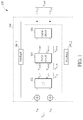
- FIG. 1 is a diagram illustrating a class-D amplifier without proposed pulse-width modulation (PWM) common-mode control according to an embodiment of the present invention.
- the class-D amplifier 100 may be a fully-differential closed-loop class-D amplifier, including a loop filter (denoted by "LF") 102, a PWM circuit 104, an output circuit 106, and a feedback circuit 108.
- LF loop filter
- PWM pulse-width modulation
- the loop filter 102 is arranged to receive an input signal VIN of the class-D amplifier 100 to generate a filtered signal VLF, wherein the input signal VIN is a fully-differential signal composed of a positive signal VIP and a negative signal VIN, and the filtered signal VLF is a fully-differential signal composed of a positive signal VLFP and a negative signal VLFN.
- the PWM circuit 104 is arranged to convert a non-PWM signal VSUM into a PWM signal VPWM.
- the non-PWM signal VSUM may be derived from the filtered signal VLF, directly or indirectly.
- the filtered signal VLF may be directly fed into the PWM circuit 104 to serve as the non-PWM signal VSUM.
- the filtered signal VLF may be processed (e.g., combined with an input feed-forward signal) before being fed into the PWM circuit 104.
- the non-PWM signal VSUM is composed of a positive signal VSUMP and a negative signal VSUMN
- the PWM signal VPWM is composed of a positive signal VPWMP and a negative signal VPWMN.
- the output circuit 106 is arranged to generate an output signal VOUT of the class-D amplifier 100 according to the PWM signal VPWM, where the output signal VOUT is composed of a positive signal VOP and a negative signal VON.
- the output circuit 106 may include a non-overlapping clock generator and an H-bridge output driver.
- the feedback circuit 108 is coupled between an output of the output circuit 106 and an input of the loop filter 102, and includes a plurality of feedback paths (e.g., feedback resistors) 109_1 and 109_2.
- the feedback paths 109_1 and 109_2 have a gain mismatch ⁇ , thus resulting in undesired terms (e.g., distortions and noise) in the differential output (VOP-VON).
- FIG. 2 is a diagram illustrating a linear model of the class-D amplifier 100 in FIG. 1 according to an embodiment of the present invention.
- the class-D amplifier 100 can be linearly modeled because the PWM switching frequency is much higher than the signal bandwidth.
- the supply noise and/or the even harmonic distortions may be represented by eC.
- the differential noise and/or the odd harmonic distortions may be represented by eD.
- the loop gain of the class-D amplifier 100 may be represented by HD (s).
- the differential output (VOP-VON) may be expressed using the following formula.
- the supply noise and/or the even harmonic distortions eC contribute ⁇ xe C to the differential output (VOP-VON).
- the differential noise and/or the odd harmonic distortions eD can be suppressed by the loop gain HD (s) .
- PSRR can only be improved by reducing the gain mismatch ⁇ .
- a stringent matching requirement of ⁇ 0.001% is required in order to achieve PSRR>100dB.
- the present invention therefore proposes applying PWM common-mode (CM) control to a class-D amplifier to suppress the supply noise and/or the even harmonic distortions at the class-D amplifier output ⁇ ⁇ e C .
- CM common-mode
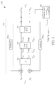
- FIG. 3 is a diagram illustrating a class-D amplifier with proposed PWM common-mode control according to an embodiment of the present invention.
- the class-D amplifier 300 may be a fully-differential closed-loop class-D amplifier, including a common-mode control circuit 302 and the aforementioned loop filter 102, PWM circuit 104, output circuit 106 and feedback circuit 108. That is, the class-D amplifier 300 shown in FIG. 3 may be created by adding the common-mode control circuit 302 to the class-D amplifier 100 shown in FIG. 1 .
- the common-mode control circuit 302 is arranged to monitor a common-mode level of the output signal VOUT (which is composed of the positive signal VOP and the negative signal VON) to generate a common-mode control signal VCM_CTRL for PWM common-mode (CM) control. For example, the common-mode level of the output signal VOUT is compared with a reference common-mode voltage VCM to set the common-mode control signal VCM_CTRL.
- VOUT which is composed of the positive signal VOP and the negative signal VON
- VCM_CTRL PWM common-mode
- FIG. 4 is a diagram illustrating a linear model of the class-D amplifier 300 in FIG. 3 according to an embodiment of the present invention.
- the class-D amplifier 300 can be linearly modeled because the PWM switching frequency is much higher than the signal bandwidth.
- the supply noise and/or the even harmonic distortions may be represented by eC.
- the differential noise and/or the odd harmonic distortions may be represented by eD.
- the loop gain of the class-D amplifier 300 may be represented by HD(s).
- the PWM common-mode control loop provided by the common-mode control circuit 302 is capable of further suppressing the supply noise and/or the even harmonic distortions at the class-D amplifier output ⁇ ⁇ e C .
- the loop gain of the PWM common-mode control loop may be represented by HC(s).
- VOP-VON The differential output (VOP-VON) may be expressed using the following formula.
- the above derivation shows that the supply noise and/or the even harmonic distortions eC are further suppressed by the loop gain HC (s) of the PWM common-mode control loop.
- the supply noise and/or the even harmonic distortions at the class-D amplifier output can be improved from ⁇ e C to ⁇ ⁇ e C H C .
- the matching requirement of the differential feedback path can be relaxed by the introduced PWM common-mode control loop.
- the proposed PWM common-mode control loop is of great help to improve the PSRR and reduce the THD+N of the fully-differential closed-loop class-D amplifier.
- the reference common-mode voltage VCM contributes ⁇ V CM to the differential output (VOP-VON) .
- a high PSRR bandgap reference voltage generator may be used to provide a bandgap reference voltage for setting the reference common-mode voltage VCM, thereby mitigating or avoiding the noise caused by the reference common-mode voltage VCM at the class-D amplifier output.
- FIG. 5 is a diagram illustrating a common-mode control circuit according to an embodiment of the present invention.
- the common-mode control circuit 302 shown in FIG. 3 may be implemented using the common-mode control circuit 500 shown in FIG. 5 .
- the common-mode control circuit 500 includes an operational amplifier circuit 502 and a reference common-mode voltage generator 504.
- the operational amplifier circuit 502 is realized by a 1st-order active-RC integrator that includes an operational amplifier OP, a capacitor C1, and a plurality of resistors R1.
- the operational amplifier circuit 502 senses an average of the class-D amplifier output (i.e., a common-mode voltage VOCM of the positive signal VOP and the negative signal VON), and compares the sensed common-mode voltage VOCM with the reference common-mode voltage VCM to output the common-mode control signal VCM_CTRL for PWM common-mode control.
- the PWM circuit 104 and the output circuit 106 both obtain the supply voltage VBAT from a battery (not shown) directly.
- the reference common-mode voltage VCM may be set by 1 2 V BAT to enlarge the output swing. As shown in FIG.
- the reference common-mode voltage generator 504 includes a plurality of circuits, such as a voltage divider, a comparator, and a digital-to-analog converter.
- the voltage divider is implemented by resistors R2 for dividing the supply voltage VBAT that is directly provided by the battery.
- the comparator CMP is arranged to compare a voltage output 1 2 V BAT of the voltage divider and a voltage output VCM of the digital-to-analog converter DAC, and generate a comparison result to a control circuit CTRL of the digital-to-analog converter DAC.
- the digital-to-analog converter DAC may be a low-rate digital-to-analog converter that operates under a low-frequency clock signal fCLK (e.g., fCLK « 217 Hz) and has a high PSRR bandgap reference voltage generator BG arranged to provide a bandgap reference voltage.
- the digital-to-analog converter DAC provides a voltage output (i.e., reference common-mode voltage VCM) according to the bandgap reference voltage. That is, the reference common-mode voltage VCM is set by the bandgap reference voltage under the control of the comparison result generated from the comparator CMP.
- the proposed PWM common-mode control is implemented to control the common-mode level of the PWM signal VPWM (which is composed of the positive signal VPWMP and the negative signal VPWMN) generated from the PWM circuit 104 to the output circuit 106.
- the PWM circuit 104 is used to convert the non-PWM signal VSUM (which is composed of the positive signal VSUMP and the negative signal VSUMN) into the PWM signal VPWM (which is composed of the positive signal VPWMP and the negative signal VPWMN) .
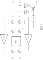
- FIG. 6 is a diagram illustrating a PWM circuit according to an embodiment of the present invention.
- the PWM circuit 104 shown in FIG. 3 may be implemented using the PWM circuit 600 shown in FIG. 6 .
- the PWM circuit 600 includes a comparing circuit (e.g., two comparators 602 and 604) and a sawtooth signal generator (or triangular wave generator) 606.
- the sawtooth signal generator 606 is a circuit designed for generating a sawtooth signal VSAW to each of the comparators 602 and 604.
- the comparator 602 is arranged to compare the positive signal VSUMP of the non-PWM signal VSUM with the sawtooth signal VSAW to generate the positive signal VPWMP of the PWM signal VPWM.
- the comparator 604 is arranged to compare the negative signal VSUMN of the non-PWM signal VSUM with the sawtooth signal VSAW to generate the negative signal VPWMN of the PWM signal VPWM.
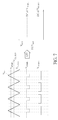
- FIG. 7 is a diagram illustrating a PWM operation performed by the PWM circuit 600 in FIG. 6 according to an embodiment of the present invention.
- SAW is the common-mode level of the sawtooth signal VSAW (i.e., the mid-point of the peak to peak voltage of the sawtooth signal VSAW).
- a negative signal VPWMN1 is generated by comparing the sawtooth signal VSAW with the fixed voltage level VSUMN1.
- a negative signal VPWMN2 is generated by comparing the sawtooth signal VSAW with the fixed voltage level VSUMN2. Since the fixed voltage level VSUMN2 is lower than the fixed voltage level VSUMN1, the duty cycle of the negative signal VPWMN1 is larger than the duty cycle of the negative signal VPWMN2. Hence, the DC level of the negative signal VPWMN1 is higher than the DC level of the negative signal VPWMN2.
- a common-mode level (DC level) of a PWM signal can be adjusted by adjusting magnitude of a non-PWM signal to be processed by pulse-width modulation. Hence, the common-mode level (DC level) of the PWM signal VPWM is affected by the common-mode level of the non-PWM signal VSUM.
- the non-PWM signal VSUM (which is composed of the positive signal VSUMP and the negative signal VSUMN) is derived from the filtered signal VLF (which is composed of the positive signal VLFP and the negative signal VLFN) . That is, the non-PWM signal VSUM may be set by the filtered signal VLF, directly or indirectly.
- the common-mode level of the non-PWM signal VSUM is affected by the common-mode level of the filtered signal VLF.
- the common-mode level (DC level) of the PWM signal VPWM is affected by the common-mode level of the filtered signal VLF.
- the proposed common-mode control circuit 302 is configured to generate the common-mode control signal VCM_CTRL to the loop filter 102 so as to adjust the common-mode level of the filtered signal VLF for achieving PWM common-mode control.
- the loop filter 102 may include one or more integrators for performing the loop filtering operation.
- the loop filter 102 may be implemented by a 3rd-order loop filter having a 1st-order integrator and a 2nd-order integrator that is cascaded to the 1st-order integrator.
- the 1st-order integrator may be a 1st-order active-RC integrator
- the 2nd-order integrator may be a 2nd-order filter that adopts the single-amplifier-biquad technique to save one operational amplifier and its associated power consumption. Since the 2nd-order integrator is the last one of cascaded integrators in the loop filter, the 2nd-order integrator (particularly, the single operational amplifier of the 2nd-order integrator) is responsible for generating the filtered signal VLF (which is composed of the positive signal VLFP and the negative signal VLFN).
- the single operational amplifier of the 2nd-order integrator may be configured to have a common-mode feedback (CMFB) circuit that is responsive to the common-mode control signal VCM_CTRL for PWM common-mode control.
- CMFB common-mode feedback
- FIG. 8 is a diagram illustrating an operational amplifier used for generating a filtered signal of a loop filter according to an embodiment of the present invention.
- the operational amplifier 800 may be the aforementioned single operational amplifier of the 2nd-order integrator that adopts the single-amplifier-biquad technique.
- the operational amplifier 800 includes a 1st-satge circuit, a 2nd-stage circuit, and a CMFB circuit.
- the 1st-satge circuit receives an input signal (VIP2, VIN2) from a preceding circuit (e.g., an output signal of the 1st-order integrator in the loop filter) .
- the 2nd-stage circuit generates and outputs the positive signal VLFP and the negative signal VLFN of the filtered signal VLF.
- the common-mode level of the filtered signal VLF generated from the 2nd-stage circuit is controlled by the CMFB circuit.
- the CMFB circuit receives the common-mode control signal VCM_CTRL from the common-mode control circuit 302, and adaptively adjusts the common-mode level of the filtered signal VLF according to the common-mode control signal VCM_CTRL.
- the non-PWM signal VSUM (which is composed of the positive signal VSUMP and the negative signal VSUMN) is derived from the filtered signal VLF (which is composed of the positive signal VLFP and the negative signal VLFN), and the common-mode level of the PWM signal VPWM is affected by the common-mode level of the non-PWM signal VSUM.
- the proposed common-mode control circuit 302 is configured to generate the common-mode control signal VCM_CTRL to a combining circuit located between the loop filter 102 and the PWM circuit 104 so as to adjust the common-mode level of the non-PWM signal VSUM for achieving PWM common-mode control.
- FIG. 9 is a diagram illustrating a combining circuit located between a loop filter and a PWM circuit according to an embodiment of the present invention.
- the class-D amplifier 300 shown in FIG. 3 may have the combining circuit 900 located between an output of the loop filter 102 and an input of the PWM circuit 104.
- the combining circuit 900 receives the common-mode control signal VCM_CTRL from the common-mode control circuit 302, and combines the filtered signal VLF (which is composed of the positive signal VLFP and the negative signal VLFN) and the common-mode control signal VCM_CTRL to generate the non-PWM signal VSUM (which is composed of the positive signal VSUMP and the negative signal VSUMN), such that the common-mode level of the non-PWM signal VSUM is adjusted/shifted by the injected common-mode control signal VCM_CTRL.
- the PWM circuit 600 compares the positive signal VSUMP and the negative signal VSUMN of the non-PWM signal VSUMP with the sawtooth signal VSAW to generate the positive signal VPWMP and the negative signal VPWMN of the PWM signal VPWM, respectively.
- the common-mode level of the PWM signal VPWM is adjusted by adjusting the common-mode level of the non-PWM signal VSUM, directly or indirectly.
- the same objective of adjusting the common-mode level of the PWM signal VPWM can be achieved by adjusting the common-mode level of the sawtooth signal VSAW (i.e., the mid-point of the peak-to-peak voltage of the sawtooth signal VSAW).
- the proposed common-mode control circuit 302 is configured to generate the common-mode control signal VCM_CTRL to a sawtooth signal generator of the PWM circuit 104 so as to adjust the common level of the sawtooth signal (i.e., the mid-point of the peak-to-peak voltage of the sawtooth signal) for achieving PWM common-mode control.
- FIG. 10 is a diagram illustrating another PWM circuit according to an embodiment of the present invention.
- the PWM circuit 104 shown in FIG. 3 may be implemented using the PWM circuit 1000 shown in FIG. 10 .
- the major difference between the PWM circuits 600 and 1000 is that the PWM circuit 1000 includes a sawtooth signal generator 1006 that is responsive to the common-mode control signal VCM_CTRL generated from the common-mode control circuit 302.
- FIG. 11 is a diagram illustrating a PWM operation performed by the PWM circuit 1000 in FIG. 10 according to an embodiment of the present invention.
- the negative signal VPWMN is set by a fixed voltage level VSUMN2.
- the common-mode level of the sawtooth signal VSAW i.e., the mid-point of the peak-to-peak voltage of the sawtooth signal VSAW
- VCM the common-mode level of the sawtooth signal
- SAW a negative signal VPWMN2 is generated by comparing the sawtooth signal VSAW with the fixed voltage level VSUMN2.
- the common-mode level of the sawtooth signal VSAW i.e., the mid-point of the peak-to-peak voltage of the sawtooth signal VSAW
- V'CM,SAW the common-mode level of the sawtooth signal VSAW
- V'CM,SAW the common-mode level of the sawtooth signal VSAW
- VCM,SAW the common-mode level of the sawtooth signal VSAW
- the duty cycle of the negative signal VPWMN1 is larger than the duty cycle of the negative signal VPWMN2.
- the DC level of the negative signal VPWMN1 is higher than the DC level of the negative signal VPWMN2.
- a common-mode level (DC level) of a PWM signal can be adjusted by adjusting magnitude of a sawtooth signal used for pulse-width modulation.
- the common-mode level (DC level) of the PWM signal VPWM is affected by the common-mode level of the sawtooth signal VSAW.
- the sawtooth signal generator 1006 adaptively adjusts/shifts the common-mode level of the sawtooth signal VSAW according to the common-mode control signal VCM_CTRL. In this way, the common-mode level (DC level) of the PWM signal VPWM generated from the PWM circuit 1000 is adjusted correspondingly.
- the class-D amplifier 300 with PWM common-mode control as illustrated in FIG. 3 is for illustrative purposes only, and is not meant to be a limitation of the present invention.
- the class-D amplifier 300 may be modified to include input feed-forward to reduce internal swing and signal-dependent terms to further enhance the linearity. More specifically, when a class-D amplifier employs the input feed-forward, internal nodes are input signal independent, and non-linearity of the loop filter has less impact on the class-D amplifier.
- FIG. 12 is a diagram illustrating another class-D amplifier with proposed PWM common-mode control according to an embodiment of the present invention.
- the class-D amplifier 1200 may be a fully-differential closed-loop class-D amplifier, including an input feed-forward circuit (e.g., two input feed-forward paths 1203 and 1204), a combining circuit 1202, and the aforementioned common-mode control circuit 302, loop filter 102, PWM circuit 104, output circuit 106 and feedback circuit 108. That is, the class-D amplifier 1200 shown in FIG. 12 may be created by adding the input feed-forward circuit (e.g., input feed-forward paths 1203 and 1204) and the combining circuit 1202 to the class-D amplifier 300 shown in FIG. 3 .
- the input feed-forward circuit (e.g., input feed-forward paths 1203 and 1204) is arranged to feed the input signal VIN to the combining circuit 1202, and the combining circuit 1202 is arranged to combine the input signal VIN and the filtered signal VLF to generate the non-PWM signal VSUM.
- the combining circuit 1202 may be composed of passive components only.
- input feed-forward with passive resistive summing can be realized by the combining circuit 1202.
- FIG. 13 is a diagram illustrating a combining circuit according to an embodiment of the present invention.
- the combining circuit 1202 shown in FIG. 12 may be implemented using the combining circuit 1300 shown in FIG. 13 .
- the combining circuit 1300 only has passive components, including resistors R7, R8 and optional capacitors C7, C8.
- the resistors R7, R8 are used to realize the input feed-forward passive summation that combines the input signal VIN (which is composed of the positive signal VIP and the negative signal VIN) and the filtered signal VLF (which is composed of the positive signal VLFP and the negative signal VLFN) to generate the non-PWM signal VPWM (which is composed of the positive signal VPWMP and the negative signal VPWMN). Since no active summing amplifier is needed by the combining circuit 1300, the power dissipation and/or the amplifier induced noise can be reduced.
- the capacitors C7 and C8 may be added to facilitate a low-pass function to filter out high-frequency noise along the signal path.
- the low-pass filter may be properly designed to reject out-of-band noise without affecting the noise transfer function (NTF) of the class-D amplifier.
- one of the aforementioned PWM common-mode control designs may be employed by the class-D amplifier 1200 for providing a common-mode gain HC to effectively suppress ⁇ ⁇ e C contributed to the differential output (VOP-VON).
- the proposed common-mode control circuit 302 is configured to generate the common-mode control signal VCM_CTRL to the loop filter 102 so as to adjust the common-mode level of the filtered signal VLF for achieving PWM common-mode control.
- the proposed common-mode control circuit 302 is configured to generate the common-mode control signal VCM_CTRL to a combining circuit located between the loop filter 102 and the PWM circuit 104 so as to adjust the common-mode level of the non-PWM signal VSUM for achieving PWM common-mode control.
- the combining circuit 1202 may be configured to combine the input signal VIN, the common-mode control signal VCM_CTRL and the filtered signal VLF to generate the non-PWM signal VSUM.
- this is for illustrative purposes only, and is not meant to be a limitation of the present invention.
- the proposed common-mode control circuit 302 is configured to generate the common-mode control signal VCM_CTRL to a sawtooth signal generator of the PWM circuit 104 so as to adjust the common-mode level of the sawtooth signal for achieving PWM common-mode control.
- the proposed PWM common-mode control mechanism is applied to a fully-differential closed-loop class-D amplifier.
- these are for illustrative purposes only, and are not meant to be limitations of the present invention.
- Any class-D amplifier design using the proposed PWM common-mode control mechanism (which may monitor a common-mode level of a differential amplifier output to generate a common-mode control signal to an internal CMFB circuit of a loop filter, an input of a PWM circuit or an internal sawtooth signal generator of the PWM circuit) falls within the scope of the present invention.
Landscapes
- Engineering & Computer Science (AREA)
- Power Engineering (AREA)
- Multimedia (AREA)
- Physics & Mathematics (AREA)
- Nonlinear Science (AREA)
- Amplifiers (AREA)
Abstract
Description
- The present invention relates to an amplifier design, and more particularly, to a class-D amplifier with pulse-width modulation (PWM) common-mode control and an associated method for performing class-D amplification according to the pre-characterizing clauses of
claims 1 and 7. - A class-D amplifier is basically a switching amplifier. It has a power efficiency approaching 100%. That is, most of the power supplied to the class-D amplifier is delivered to the load. Conventionally, a low-dropout (LDO) regulator with high power supply rejection ratio (PSRR) is adopted to supply a clean power to the class-D amplifier. This LDO is used to mitigate the noise coupling through or generated from the power management circuit that may include buck/boost converters. However, this LDO causes additional power loss and decreases the energy efficiency of the whole system. Therefore, in order to avoid this undesired power loss, the supply voltage of a class-D amplifier is preferred to be powered by a power source (e.g., a battery) without using a LDO, which lays critical emphasis on the PSRR of the Class-D audio amplifier. Consequently, for high performance of audio applications, there is a need for an innovative class-D amplifier (CDA) design with high power-supply rejection ratio (PSRR) and high linearity (e.g., low Total Harmonic Distortion with Noise (THD+N)).
- One of the objectives of the claimed invention is to provide a class-D amplifier with pulse-width modulation (PWM) common-mode control and an associated method for performing class-D amplification.
- According to a first aspect of the present invention, an exemplary class-D amplifier is disclosed. The exemplary class-D amplifier includes a loop filter, a pulse-width modulation (PWM) circuit, an output circuit, and a common-mode control circuit. The loop filter is arranged to receive an input signal of the class-D amplifier to generate a filtered signal. The PWM circuit is arranged to convert a non-PWM signal into a PWM signal, wherein the non-PWM signal is derived from at least the filtered signal. The output circuit is arranged to generate an output signal of the class-D amplifier according to the PWM signal. The common-mode control circuit is arranged to monitor a common-mode level of the output signal to generate a common-mode control signal for PWM common-mode control.
- According to a second aspect of the present invention, an exemplary class-D amplifier is disclosed. The exemplary class-D amplifier includes a loop filter, a combining circuit, an input feed-forward circuit, a pulse-width modulation (PWM) circuit, and an output circuit. The loop filter is arranged to receive an input signal of the class-D amplifier to generate a filtered signal. The combining circuit is arranged to combine at least the filtered signal and the input signal to generate a non-PWM signal, wherein the combining circuit is composed of passive components only. The input feed-forward circuit is arranged to feed the input signal to the combining circuit. The PWM circuit is arranged to convert the non-PWM signal into a PWM signal. The output circuit is arranged to generate an output signal of the class-D amplifier according to the PWM signal.
- According to a third aspect of the present invention, an exemplary method for performing class-D amplification is disclosed. The exemplary method includes: performing a loop filtering operation upon an input signal of the class-D amplification to generate a filtered signal; performing a pulse-width modulation (PWM) operation to convert a non-PWM signal into a PWM signal, wherein the non-PWM signal is derived from at least the filtered signal; generating an output signal of the class-D amplification according to the PWM signal; and monitoring a common-mode level of the output signal to generate a common-mode control signal for PWM common-mode control.
- According to a fourth aspect of the present invention, an exemplary method for performing class-D amplification is disclosed. The exemplary method includes: performing a loop filtering operation upon an input signal of the class-D amplification to generate a filtered signal; utilizing a combining circuit to combine at least the filtered signal and the input signal to generate a non-PWM signal, wherein the combining circuit is composed of passive components only; performing a pulse-width modulation (PWM) operation to convert the non-PWM signal into a PWM signal; and generating an output signal of the class-D amplifier according to the PWM signal.
- In the following, the invention is further illustrated by way of example, taking reference to the accompanying drawings.
-
FIG. 1 is a diagram illustrating a class-D amplifier without proposed pulse-width modulation (PWM) common-mode control according to an embodiment of the present invention, -
FIG. 2 is a diagram illustrating a linear model of the class-D amplifier inFIG. 1 according to an embodiment of the present invention, -
FIG. 3 is a diagram illustrating a class-D amplifier with proposed PWM common-mode control according to an embodiment of the present invention, -
FIG. 4 is a diagram illustrating a linear model of the class-D amplifier inFIG. 3 according to an embodiment of the present invention, -
FIG. 5 is a diagram illustrating a common-mode control circuit according to an embodiment of the present invention, -
FIG. 6 is a diagram illustrating a PWM circuit according to an embodiment of the present invention, -
FIG. 7 is a diagram illustrating a PWM operation performed by the PWM circuit inFIG. 6 according to an embodiment of the present invention, -
FIG. 8 is a diagram illustrating an operational amplifier used for generating a filtered signal of a loop filter according to an embodiment of the present invention, -
FIG. 9 is a diagram illustrating a combining circuit located between a loop filter and a PWM circuit according to an embodiment of the present invention, -
FIG. 10 is a diagram illustrating another PWM circuit according to an embodiment of the present invention, -
FIG. 11 is a diagram illustrating a PWM operation performed by the PWM circuit inFIG. 10 according to an embodiment of the present invention, -
FIG. 12 is a diagram illustrating another class-D amplifier with proposed PWM common-mode control according to an embodiment of the present invention, and -
FIG. 13 is a diagram illustrating a combining circuit according to an embodiment of the present invention. - Certain terms are used throughout the following description and claims, which refer to particular components. As one skilled in the art will appreciate, electronic equipment manufacturers may refer to a component by different names. This document does not intend to distinguish between components that differ in name but not in function. In the following description and in the claims, the terms "include" and "comprise" are used in an open-ended fashion, and thus should be interpreted to mean "include, but not limited to ... ". Also, the term "couple" is intended to mean either an indirect or direct electrical connection. Accordingly, if one device is coupled to another device, that connection may be through a direct electrical connection, or through an indirect electrical connection via other devices and connections.
-
FIG. 1 is a diagram illustrating a class-D amplifier without proposed pulse-width modulation (PWM) common-mode control according to an embodiment of the present invention. The class-D amplifier 100 may be a fully-differential closed-loop class-D amplifier, including a loop filter (denoted by "LF") 102, aPWM circuit 104, anoutput circuit 106, and afeedback circuit 108. Theloop filter 102 is arranged to receive an input signal VIN of the class-D amplifier 100 to generate a filtered signal VLF, wherein the input signal VIN is a fully-differential signal composed of a positive signal VIP and a negative signal VIN, and the filtered signal VLF is a fully-differential signal composed of a positive signal VLFP and a negative signal VLFN. ThePWM circuit 104 is arranged to convert a non-PWM signal VSUM into a PWM signal VPWM. The non-PWM signal VSUM may be derived from the filtered signal VLF, directly or indirectly. For example, the filtered signal VLF may be directly fed into thePWM circuit 104 to serve as the non-PWM signal VSUM. For another example, the filtered signal VLF may be processed (e.g., combined with an input feed-forward signal) before being fed into thePWM circuit 104. The non-PWM signal VSUM is composed of a positive signal VSUMP and a negative signal VSUMN, and the PWM signal VPWM is composed of a positive signal VPWMP and a negative signal VPWMN. Theoutput circuit 106 is arranged to generate an output signal VOUT of the class-D amplifier 100 according to the PWM signal VPWM, where the output signal VOUT is composed of a positive signal VOP and a negative signal VON. For example, theoutput circuit 106 may include a non-overlapping clock generator and an H-bridge output driver. Thefeedback circuit 108 is coupled between an output of theoutput circuit 106 and an input of theloop filter 102, and includes a plurality of feedback paths (e.g., feedback resistors) 109_1 and 109_2. In an actual implementation, the feedback paths 109_1 and 109_2 have a gain mismatch δ, thus resulting in undesired terms (e.g., distortions and noise) in the differential output (VOP-VON). -
FIG. 2 is a diagram illustrating a linear model of the class-D amplifier 100 inFIG. 1 according to an embodiment of the present invention. The class-D amplifier 100 can be linearly modeled because the PWM switching frequency is much higher than the signal bandwidth. The supply noise and/or the even harmonic distortions may be represented by eC. The differential noise and/or the odd harmonic distortions may be represented by eD. The loop gain of the class-D amplifier 100 may be represented by HD (s). The differential output (VOP-VON) may be expressed using the following formula.
- With the gain mismatch δ of the differential feedback path, the supply noise and/or the even harmonic distortions eC contribute δxeC to the differential output (VOP-VON). The differential noise and/or the odd harmonic distortions eD can be suppressed by the loop gain HD (s) . PSRR can only be improved by reducing the gain mismatch δ. For example, a stringent matching requirement of δ<0.001% is required in order to achieve PSRR>100dB. However, it is very hard to meet the stringent matching requirement of δ<0.001% in the real world. The present invention therefore proposes applying PWM common-mode (CM) control to a class-D amplifier to suppress the supply noise and/or the even harmonic distortions at the class-D amplifier output δ × eC .
-
FIG. 3 is a diagram illustrating a class-D amplifier with proposed PWM common-mode control according to an embodiment of the present invention. The class-D amplifier 300 may be a fully-differential closed-loop class-D amplifier, including a common-mode control circuit 302 and theaforementioned loop filter 102,PWM circuit 104,output circuit 106 andfeedback circuit 108. That is, the class-D amplifier 300 shown inFIG. 3 may be created by adding the common-mode control circuit 302 to the class-D amplifier 100 shown inFIG. 1 . In this embodiment, the common-mode control circuit 302 is arranged to monitor a common-mode level of the output signal VOUT (which is composed of the positive signal VOP and the negative signal VON) to generate a common-mode control signal VCM_CTRL for PWM common-mode (CM) control. For example, the common-mode level of the output signal VOUT is compared with a reference common-mode voltage VCM to set the common-mode control signal VCM_CTRL. -
FIG. 4 is a diagram illustrating a linear model of the class-D amplifier 300 inFIG. 3 according to an embodiment of the present invention. The class-D amplifier 300 can be linearly modeled because the PWM switching frequency is much higher than the signal bandwidth. The supply noise and/or the even harmonic distortions may be represented by eC. The differential noise and/or the odd harmonic distortions may be represented by eD. The loop gain of the class-D amplifier 300 may be represented by HD(s). The PWM common-mode control loop provided by the common-mode control circuit 302 is capable of further suppressing the supply noise and/or the even harmonic distortions at the class-D amplifier output δ ×eC . The loop gain of the PWM common-mode control loop may be represented by HC(s). The differential output (VOP-VON) may be expressed using the following formula.
- The above derivation shows that the supply noise and/or the even harmonic distortions eC are further suppressed by the loop gain HC (s) of the PWM common-mode control loop. Hence, the supply noise and/or the even harmonic distortions at the class-D amplifier output can be improved from δ×eC to

-
FIG. 5 is a diagram illustrating a common-mode control circuit according to an embodiment of the present invention. For example, the common-mode control circuit 302 shown inFIG. 3 may be implemented using the common-mode control circuit 500 shown inFIG. 5 . The common-mode control circuit 500 includes anoperational amplifier circuit 502 and a reference common-mode voltage generator 504. In this embodiment, theoperational amplifier circuit 502 is realized by a 1st-order active-RC integrator that includes an operational amplifier OP, a capacitor C1, and a plurality of resistors R1. Theoperational amplifier circuit 502 senses an average of the class-D amplifier output (i.e., a common-mode voltage VOCM of the positive signal VOP and the negative signal VON), and compares the sensed common-mode voltage VOCM with the reference common-mode voltage VCM to output the common-mode control signal VCM_CTRL for PWM common-mode control. In one exemplary embodiment, thePWM circuit 104 and theoutput circuit 106 both obtain the supply voltage VBAT from a battery (not shown) directly. Hence, the reference common-mode voltage VCM may be set by
FIG. 5 , the reference common-mode voltage generator 504 includes a plurality of circuits, such as a voltage divider, a comparator, and a digital-to-analog converter. The voltage divider is implemented by resistors R2 for dividing the supply voltage VBAT that is directly provided by the battery. The comparator CMP is arranged to compare avoltage output 

- The proposed PWM common-mode control is implemented to control the common-mode level of the PWM signal VPWM (which is composed of the positive signal VPWMP and the negative signal VPWMN) generated from the
PWM circuit 104 to theoutput circuit 106. ThePWM circuit 104 is used to convert the non-PWM signal VSUM (which is composed of the positive signal VSUMP and the negative signal VSUMN) into the PWM signal VPWM (which is composed of the positive signal VPWMP and the negative signal VPWMN) .FIG. 6 is a diagram illustrating a PWM circuit according to an embodiment of the present invention. ThePWM circuit 104 shown inFIG. 3 may be implemented using thePWM circuit 600 shown inFIG. 6 . ThePWM circuit 600 includes a comparing circuit (e.g., twocomparators 602 and 604) and a sawtooth signal generator (or triangular wave generator) 606. Thesawtooth signal generator 606 is a circuit designed for generating a sawtooth signal VSAW to each of thecomparators comparator 602 is arranged to compare the positive signal VSUMP of the non-PWM signal VSUM with the sawtooth signal VSAW to generate the positive signal VPWMP of the PWM signal VPWM. Thecomparator 604 is arranged to compare the negative signal VSUMN of the non-PWM signal VSUM with the sawtooth signal VSAW to generate the negative signal VPWMN of the PWM signal VPWM.FIG. 7 is a diagram illustrating a PWM operation performed by thePWM circuit 600 inFIG. 6 according to an embodiment of the present invention. Take the generation of the negative signal VPWMN for example. Assume VCM, SAW is the common-mode level of the sawtooth signal VSAW (i.e., the mid-point of the peak to peak voltage of the sawtooth signal VSAW). In a case where the negative signal VPWMN is set by the fixed voltage level VSUMN1, a negative signal VPWMN1 is generated by comparing the sawtooth signal VSAW with the fixed voltage level VSUMN1. In another case where the negative signal VPWMN is set by the fixed voltage level VSUMN2, a negative signal VPWMN2 is generated by comparing the sawtooth signal VSAW with the fixed voltage level VSUMN2. Since the fixed voltage level VSUMN2 is lower than the fixed voltage level VSUMN1, the duty cycle of the negative signal VPWMN1 is larger than the duty cycle of the negative signal VPWMN2. Hence, the DC level of the negative signal VPWMN1 is higher than the DC level of the negative signal VPWMN2. As can be seen fromFIG. 7 , a common-mode level (DC level) of a PWM signal can be adjusted by adjusting magnitude of a non-PWM signal to be processed by pulse-width modulation. Hence, the common-mode level (DC level) of the PWM signal VPWM is affected by the common-mode level of the non-PWM signal VSUM. - The non-PWM signal VSUM (which is composed of the positive signal VSUMP and the negative signal VSUMN) is derived from the filtered signal VLF (which is composed of the positive signal VLFP and the negative signal VLFN) . That is, the non-PWM signal VSUM may be set by the filtered signal VLF, directly or indirectly. Hence, the common-mode level of the non-PWM signal VSUM is affected by the common-mode level of the filtered signal VLF. Accordingly, the common-mode level (DC level) of the PWM signal VPWM is affected by the common-mode level of the filtered signal VLF.
- In a first exemplary PWM common-mode control design, the proposed common-
mode control circuit 302 is configured to generate the common-mode control signal VCM_CTRL to theloop filter 102 so as to adjust the common-mode level of the filtered signal VLF for achieving PWM common-mode control. Theloop filter 102 may include one or more integrators for performing the loop filtering operation. For example, theloop filter 102 may be implemented by a 3rd-order loop filter having a 1st-order integrator and a 2nd-order integrator that is cascaded to the 1st-order integrator. In one exemplary implementation, the 1st-order integrator may be a 1st-order active-RC integrator, and the 2nd-order integrator may be a 2nd-order filter that adopts the single-amplifier-biquad technique to save one operational amplifier and its associated power consumption. Since the 2nd-order integrator is the last one of cascaded integrators in the loop filter, the 2nd-order integrator (particularly, the single operational amplifier of the 2nd-order integrator) is responsible for generating the filtered signal VLF (which is composed of the positive signal VLFP and the negative signal VLFN). The single operational amplifier of the 2nd-order integrator may be configured to have a common-mode feedback (CMFB) circuit that is responsive to the common-mode control signal VCM_CTRL for PWM common-mode control. -
FIG. 8 is a diagram illustrating an operational amplifier used for generating a filtered signal of a loop filter according to an embodiment of the present invention. Theoperational amplifier 800 may be the aforementioned single operational amplifier of the 2nd-order integrator that adopts the single-amplifier-biquad technique. As shown inFIG. 8 , theoperational amplifier 800 includes a 1st-satge circuit, a 2nd-stage circuit, and a CMFB circuit. The 1st-satge circuit receives an input signal (VIP2, VIN2) from a preceding circuit (e.g., an output signal of the 1st-order integrator in the loop filter) . The 2nd-stage circuit generates and outputs the positive signal VLFP and the negative signal VLFN of the filtered signal VLF. The common-mode level of the filtered signal VLF generated from the 2nd-stage circuit is controlled by the CMFB circuit. In this embodiment, the CMFB circuit receives the common-mode control signal VCM_CTRL from the common-mode control circuit 302, and adaptively adjusts the common-mode level of the filtered signal VLF according to the common-mode control signal VCM_CTRL. - As mentioned above, the non-PWM signal VSUM (which is composed of the positive signal VSUMP and the negative signal VSUMN) is derived from the filtered signal VLF (which is composed of the positive signal VLFP and the negative signal VLFN), and the common-mode level of the PWM signal VPWM is affected by the common-mode level of the non-PWM signal VSUM. In a second exemplary PWM common-mode control design, the proposed common-
mode control circuit 302 is configured to generate the common-mode control signal VCM_CTRL to a combining circuit located between theloop filter 102 and thePWM circuit 104 so as to adjust the common-mode level of the non-PWM signal VSUM for achieving PWM common-mode control. -
FIG. 9 is a diagram illustrating a combining circuit located between a loop filter and a PWM circuit according to an embodiment of the present invention. For example, the class-D amplifier 300 shown inFIG. 3 may have the combiningcircuit 900 located between an output of theloop filter 102 and an input of thePWM circuit 104. In this embodiment, the combiningcircuit 900 receives the common-mode control signal VCM_CTRL from the common-mode control circuit 302, and combines the filtered signal VLF (which is composed of the positive signal VLFP and the negative signal VLFN) and the common-mode control signal VCM_CTRL to generate the non-PWM signal VSUM (which is composed of the positive signal VSUMP and the negative signal VSUMN), such that the common-mode level of the non-PWM signal VSUM is adjusted/shifted by the injected common-mode control signal VCM_CTRL. - As illustrated in
FIG. 6 , thePWM circuit 600 compares the positive signal VSUMP and the negative signal VSUMN of the non-PWM signal VSUMP with the sawtooth signal VSAW to generate the positive signal VPWMP and the negative signal VPWMN of the PWM signal VPWM, respectively. In above exemplary designs, the common-mode level of the PWM signal VPWM is adjusted by adjusting the common-mode level of the non-PWM signal VSUM, directly or indirectly. Since the sawtooth signal VSAW is also involved in generating the PWM signal VPWM, the same objective of adjusting the common-mode level of the PWM signal VPWM can be achieved by adjusting the common-mode level of the sawtooth signal VSAW (i.e., the mid-point of the peak-to-peak voltage of the sawtooth signal VSAW). In a third exemplary PWM common-mode control design, the proposed common-mode control circuit 302 is configured to generate the common-mode control signal VCM_CTRL to a sawtooth signal generator of thePWM circuit 104 so as to adjust the common level of the sawtooth signal (i.e., the mid-point of the peak-to-peak voltage of the sawtooth signal) for achieving PWM common-mode control. -
FIG. 10 is a diagram illustrating another PWM circuit according to an embodiment of the present invention. ThePWM circuit 104 shown inFIG. 3 may be implemented using thePWM circuit 1000 shown inFIG. 10 . The major difference between thePWM circuits PWM circuit 1000 includes asawtooth signal generator 1006 that is responsive to the common-mode control signal VCM_CTRL generated from the common-mode control circuit 302. -
FIG. 11 is a diagram illustrating a PWM operation performed by thePWM circuit 1000 inFIG. 10 according to an embodiment of the present invention. Take the generation of the negative signal VPWMN for example. Assume that the negative signal VPWMN is set by a fixed voltage level VSUMN2. In a case where the common-mode level of the sawtooth signal VSAW (i.e., the mid-point of the peak-to-peak voltage of the sawtooth signal VSAW) is set by VCM, SAW, a negative signal VPWMN2 is generated by comparing the sawtooth signal VSAW with the fixed voltage level VSUMN2. In another case where the common-mode level of the sawtooth signal VSAW (i.e., the mid-point of the peak-to-peak voltage of the sawtooth signal VSAW) is set by V'CM,SAW, a negative signal VPWMN1 is generated by comparing the sawtooth signal VSAW with the fixed voltage level VSUMN2. Since the common-mode level V'CM, SAW is lower than the common-mode level VCM,SAW, the duty cycle of the negative signal VPWMN1 is larger than the duty cycle of the negative signal VPWMN2. Hence, the DC level of the negative signal VPWMN1 is higher than the DC level of the negative signal VPWMN2. As can be seen fromFIG. 11 , a common-mode level (DC level) of a PWM signal can be adjusted by adjusting magnitude of a sawtooth signal used for pulse-width modulation. Hence, the common-mode level (DC level) of the PWM signal VPWM is affected by the common-mode level of the sawtooth signal VSAW. Based on the above observation, thesawtooth signal generator 1006 adaptively adjusts/shifts the common-mode level of the sawtooth signal VSAW according to the common-mode control signal VCM_CTRL. In this way, the common-mode level (DC level) of the PWM signal VPWM generated from thePWM circuit 1000 is adjusted correspondingly. - The class-
D amplifier 300 with PWM common-mode control as illustrated inFIG. 3 is for illustrative purposes only, and is not meant to be a limitation of the present invention. For example, the class-D amplifier 300 may be modified to include input feed-forward to reduce internal swing and signal-dependent terms to further enhance the linearity. More specifically, when a class-D amplifier employs the input feed-forward, internal nodes are input signal independent, and non-linearity of the loop filter has less impact on the class-D amplifier.FIG. 12 is a diagram illustrating another class-D amplifier with proposed PWM common-mode control according to an embodiment of the present invention. The class-D amplifier 1200 may be a fully-differential closed-loop class-D amplifier, including an input feed-forward circuit (e.g., two input feed-forward paths 1203 and 1204), a combiningcircuit 1202, and the aforementioned common-mode control circuit 302,loop filter 102,PWM circuit 104,output circuit 106 andfeedback circuit 108. That is, the class-D amplifier 1200 shown inFIG. 12 may be created by adding the input feed-forward circuit (e.g., input feed-forward paths 1203 and 1204) and the combiningcircuit 1202 to the class-D amplifier 300 shown inFIG. 3 . In this embodiment, the input feed-forward circuit (e.g., input feed-forward paths 1203 and 1204) is arranged to feed the input signal VIN to the combiningcircuit 1202, and the combiningcircuit 1202 is arranged to combine the input signal VIN and the filtered signal VLF to generate the non-PWM signal VSUM. - In one exemplary embodiment, the combining
circuit 1202 may be composed of passive components only. Hence, input feed-forward with passive resistive summing can be realized by the combiningcircuit 1202.FIG. 13 is a diagram illustrating a combining circuit according to an embodiment of the present invention. The combiningcircuit 1202 shown inFIG. 12 may be implemented using the combiningcircuit 1300 shown inFIG. 13 . The combiningcircuit 1300 only has passive components, including resistors R7, R8 and optional capacitors C7, C8. The resistors R7, R8 are used to realize the input feed-forward passive summation that combines the input signal VIN (which is composed of the positive signal VIP and the negative signal VIN) and the filtered signal VLF (which is composed of the positive signal VLFP and the negative signal VLFN) to generate the non-PWM signal VPWM (which is composed of the positive signal VPWMP and the negative signal VPWMN). Since no active summing amplifier is needed by the combiningcircuit 1300, the power dissipation and/or the amplifier induced noise can be reduced. The capacitors C7 and C8 may be added to facilitate a low-pass function to filter out high-frequency noise along the signal path. The low-pass filter may be properly designed to reject out-of-band noise without affecting the noise transfer function (NTF) of the class-D amplifier. - Similarly, one of the aforementioned PWM common-mode control designs may be employed by the class-
D amplifier 1200 for providing a common-mode gain HC to effectively suppress δ×eC contributed to the differential output (VOP-VON). When the first exemplary PWM common-mode control design is employed, the proposed common-mode control circuit 302 is configured to generate the common-mode control signal VCM_CTRL to theloop filter 102 so as to adjust the common-mode level of the filtered signal VLF for achieving PWM common-mode control. When the second exemplary PWM common-mode control design is employed, the proposed common-mode control circuit 302 is configured to generate the common-mode control signal VCM_CTRL to a combining circuit located between theloop filter 102 and thePWM circuit 104 so as to adjust the common-mode level of the non-PWM signal VSUM for achieving PWM common-mode control. For example, the combiningcircuit 1202 may be configured to combine the input signal VIN, the common-mode control signal VCM_CTRL and the filtered signal VLF to generate the non-PWM signal VSUM. However, this is for illustrative purposes only, and is not meant to be a limitation of the present invention. When the third exemplary PWM common-mode control design is employed, the proposed common-mode control circuit 302 is configured to generate the common-mode control signal VCM_CTRL to a sawtooth signal generator of thePWM circuit 104 so as to adjust the common-mode level of the sawtooth signal for achieving PWM common-mode control. - In above embodiments, the proposed PWM common-mode control mechanism is applied to a fully-differential closed-loop class-D amplifier. However, these are for illustrative purposes only, and are not meant to be limitations of the present invention. Any class-D amplifier design using the proposed PWM common-mode control mechanism (which may monitor a common-mode level of a differential amplifier output to generate a common-mode control signal to an internal CMFB circuit of a loop filter, an input of a PWM circuit or an internal sawtooth signal generator of the PWM circuit) falls within the scope of the present invention.
- Those skilled in the art will readily observe that numerous modifications and alterations of the device and method may be made while retaining the teachings of the invention. Accordingly, the above disclosure should be construed as limited only by the metes and bounds of the appended claims.
Claims (15)
- A class-D amplifier (100, 300, 1200), characterized by:a loop filter (102), arranged to receive an input signal (Vin) of the class-D amplifier (100, 300, 1200) to generate a filtered signal (VLF);a pulse-width modulation circuit (106, 600, 1000), hereinafter PWM circuit, arranged to convert a non-PWM signal (VSUM) into a PWM signal (VPWM), wherein the non-PWM signal (VSUM) is derived from at least the filtered signal (VLF);an output circuit (106), arranged to generate an output signal (VOUT) of the class-D amplifier (100, 300, 1200) according to the PWM signal (VPWM); anda common-mode control circuit (302, 500), arranged to monitor a common-mode level of the output signal (VOUT) to generate a common-mode control signal (VCM_CTRL) for PWM common-mode control.
- The class-D amplifier(100, 300, 1200) of claim 1, characterized in that the loop filter (102) comprises a common-mode feedback circuit, hereinafter CMFB circuit; the common-mode control circuit (302, 500) is arranged to output the common-mode control signal (VCM_CTRL) to the CMFB circuit of the loop filter (102); and the CMFB circuit of the loop filter (102) is arranged to adjust a common-mode level of the filtered signal (VLF) according to the common-mode control signal (VCM_CTRL).
- The class-D amplifier (100, 300) of claim 1, characterized in that the class-D amplifier (100, 300) further comprises:a combining circuit (900), located between an output of the loop filter and an input of the PWM circuit;wherein the common-mode control circuit (302, 500) is arranged to output the common-mode control signal (VCM_CTRL) to the combining circuit (900); and the combining circuit (900) is arranged to combine the filtered signal (VLF) and the common-mode control signal (VCM_CTRL) to adjust a common-mode level of the non-PWM signal (VSUM), where the non-PWM signal (VSUM) is derived from combining at least the filtered signal (VLF) and the common-mode control signal (VCM_CTRL).
- The class-D amplifier (100, 300) of claim 1, characterized in that the PWM circuit (1000) comprises:a sawtooth signal generator (1006), arranged to generate a sawtooth signal (VSAW); anda comparing circuit (602, 604), arranged to compare the non-PWM signal (VSUM) with the sawtooth signal (VSAW) to generate the PWM signal (VPWM);wherein the common-mode control circuit (302, 500) is arranged to output the common-mode control signal (VCM_CTRL) to the sawtooth signal generator (1006); and the sawtooth signal generator (1006) is further arranged to adjust a common-mode level of the sawtooth signal (VSAW) according to the common-mode control signal (VCM_CTRL).
- The class-D amplifier (100, 300) of claim 1, characterized in that the common-mode control circuit comprises:a reference common-mode voltage generator (504), arranged to monitor a supply voltage (VBAT) of the class-D amplifier to generate a reference common-mode voltage (VCM); andan operational amplifier circuit (502), arranged to output the common-mode control signal (VCM_CTRL) according to the common-mode level of the output signal (VOUT) and the reference common-mode voltage (VCM).
- The class-D amplifier (1200) of claim 1, characterized in that the class-D amplifier (1200) further comprises:a combining circuit (1202), located between an output of the loop filter (102) and an input of the PWM circuit (104); andan input feed-forward circuit (1203, 1204), arranged to feed the input signal (VIN) to the combining circuit (1202);wherein the combining circuit (1202) is arranged to combine at least the filtered signal (VLF) and the input signal (VIN) to generate the non-PWM signal (VSUM), and the combining circuit (1202) is composed of passive components only.
- A method for performing class-D amplification, characterized by:performing a loop filtering operation upon an input signal (VIN) of the class-D amplification to generate a filtered signal (VLF);performing a pulse-width modulation, hereinafter PWM, operation to convert a non-PWM signal (VSUM) into a PWM signal (VPWM), wherein the non-PWM signal (VSUM) is derived from at least the filtered signal (VLF);generating an output signal (VOUT) of the class-D amplification according to the PWM signal (VPWM); andmonitoring a common-mode level of the output signal (VOUT) to generate a common-mode control signal (VCM_CTRL) for PWM common-mode control.
- The method of claim7, characterized in that monitoring the common-mode level of the output signal (VOUT) to generate the common-mode control signal (VCM_CTRL) for PWM common-mode control comprises:feeding the common-mode control signal (VCM_CTRL) to a common-mode feedback, hereinafter CMFB, function of the loop filtering operation, wherein the CMFB function of the loop filtering operation adjusts a common-mode level of the filtered signal (VLF) according to the common-mode control signal (VCM_CTRL).
- The method of claim 7, characterized in that the non-PWM signal (VSUM) is derived from at least the filtered signal (VLF) and the common-mode control signal (VCM_CTRL), and the method further comprises:combining the filtered signal (VLF) and the common-mode control signal (VCM_CTRL) to adjust a common-mode level of the non-PWM signal (VSUM), where the non-PWM signal (VSUM) is derived from combining at least the filtered signal (VLF) and the common-mode control signal (VCM_CTRL).
- The method of claim 7, characterized in that the PWM operation comprises:generating a sawtooth signal (VSAW);adjusting a common-mode level of the sawtooth signal (VSAW) according to the common-mode control signal (VCM_CTRL) ; andcomparing the non-PWM signal (VSUM) with the sawtooth signal (VSAW) to generate the PWM signal (VPWM).
- The method of claim 7, characterized in that monitoring the common-mode level of the output signal (VOUT) to generate the common-mode control signal (VCM_CTRL) for PWM common-mode control comprises:monitoring a supply voltage (VBAT) to generate a reference common-mode voltage (VCM); andcomparing the common-mode level of the output signal (VOUT) with the reference common-mode voltage (VCM) to output the common-mode control signal (VCM_CTRL).
- The method of claim 11, characterized in that monitoring the supply voltage (VBAT) to generate the reference common-mode voltage (VCM) comprises:providing a bandgap reference voltage; andderiving the reference common-mode voltage (VCM) from the bandgap reference voltage according to the monitored supply voltage (VBAT).
- The method of claim 7, characterized in that the method further comprises:utilizing a combining circuit (1202) to combine at least the filtered signal (VLF) and the input signal (VIN) to generate the non-PWM signal (VSUM);wherein the combining circuit (1202) is composed of passive components only.
- The method of claim 13, characterized in that the passive components comprise resistors for performing input feed-forward resistive summation.
- The method of claim 7, characterized in that the class-D amplification is fully-differential closed-loop class-D amplification, and the method further comprises:feeding back the output signal (VOUT) to the loop filtering operation.
Applications Claiming Priority (3)
| Application Number | Priority Date | Filing Date | Title |
|---|---|---|---|
| US201562217178P | 2015-09-11 | 2015-09-11 | |
| US201562218744P | 2015-09-15 | 2015-09-15 | |
| US15/257,939 US10027294B2 (en) | 2015-09-11 | 2016-09-07 | Class-D amplifier with pulse-width modulation common-mode control and associated method for performing class-D amplification |
Publications (3)
| Publication Number | Publication Date |
|---|---|
| EP3142251A2 true EP3142251A2 (en) | 2017-03-15 |
| EP3142251A3 EP3142251A3 (en) | 2017-06-07 |
| EP3142251B1 EP3142251B1 (en) | 2020-03-04 |
Family
ID=56893812
Family Applications (1)
| Application Number | Title | Priority Date | Filing Date |
|---|---|---|---|
| EP16187817.8A Active EP3142251B1 (en) | 2015-09-11 | 2016-09-08 | Class-d amplifier with pulse-width modulation common-mode control and associated method for performing class-d amplification |
Country Status (3)
| Country | Link |
|---|---|
| US (1) | US10027294B2 (en) |
| EP (1) | EP3142251B1 (en) |
| CN (1) | CN107046404B (en) |
Cited By (3)
| Publication number | Priority date | Publication date | Assignee | Title |
|---|---|---|---|---|
| EP3588774A1 (en) * | 2018-06-29 | 2020-01-01 | Linear Technology Holding LLC | Differential load controller |
| CN116166081A (en) * | 2023-03-20 | 2023-05-26 | 中国科学院微电子研究所 | Low-dropout linear voltage regulator with high power supply rejection ratio and implementation method thereof |
| TWI818579B (en) * | 2021-12-14 | 2023-10-11 | 立錡科技股份有限公司 | Pulse width modulation method |
Families Citing this family (18)
| Publication number | Priority date | Publication date | Assignee | Title |
|---|---|---|---|---|
| US10224877B2 (en) | 2017-01-20 | 2019-03-05 | Cirrus Logic, Inc. | Closed-loop digital compensation scheme |
| GB2562125B (en) * | 2017-01-20 | 2019-09-18 | Cirrus Logic Int Semiconductor Ltd | Closed-loop digital compensation scheme |
| US10236827B2 (en) | 2017-01-20 | 2019-03-19 | Cirrus Logic, Inc. | Offset calibration for amplifier and preceding circuit |
| KR102300544B1 (en) * | 2017-04-07 | 2021-09-09 | (주)드림어스컴퍼니 | Modularized Signal Converting Apparatus and Method thereof |
| US10396724B1 (en) | 2018-05-30 | 2019-08-27 | Semiconductor Components Industries, Llc | Amplifier with common mode loop and chop |
| CN109217827B (en) * | 2018-08-31 | 2022-07-01 | 南京矽力微电子技术有限公司 | D-type power amplifier, compensation method thereof and digital signal processing device |
| US11082019B2 (en) | 2020-01-07 | 2021-08-03 | Semiconductor Components Industries, Llc | Amplifier with adaptively-controlled local feedback loop |
| US11398802B2 (en) * | 2020-03-25 | 2022-07-26 | Bose Corporation | Common mode voltage controller for self-boosting push pull amplifier |
| CN111726091B (en) * | 2020-08-03 | 2024-07-19 | 广芯电子技术(上海)股份有限公司 | Class D audio power amplifier |
| US11323082B2 (en) | 2020-08-10 | 2022-05-03 | Elite Semiconductor Microelectronics Technology Inc. | Class-D amplifier which can suppress differential mode power noise |
| TWI724979B (en) * | 2020-10-12 | 2021-04-11 | 晶豪科技股份有限公司 | Class-d amplifier which can suppress differential mode power noise |
| CN114430254A (en) * | 2020-10-28 | 2022-05-03 | 晶豪科技股份有限公司 | D-class amplifier capable of suppressing noise of differential mode power supply |
| CN112910427A (en) * | 2021-01-13 | 2021-06-04 | 上海艾为电子技术股份有限公司 | Class D audio amplifier, adaptive pulse width adjusting method thereof and electronic equipment |
| US12308807B2 (en) * | 2021-02-05 | 2025-05-20 | Mediatek Inc. | Amplification circuit with compensation for common-mode voltage fluctuation |
| TWI831102B (en) * | 2021-12-16 | 2024-02-01 | 瑞昱半導體股份有限公司 | Audio signal modulation and amplification circuit |
| CN116346043B (en) * | 2021-12-23 | 2025-11-25 | 瑞昱半导体股份有限公司 | Audio modulation amplifier circuit |
| US12028030B2 (en) * | 2022-01-26 | 2024-07-02 | Qualcomm Incorporated | Dynamic common-mode adjustment for power amplifiers |
| CN114531117A (en) * | 2022-02-18 | 2022-05-24 | 苏州至盛半导体科技有限公司 | Common-mode voltage dynamic modulation circuit and method and class D audio power amplifier |
Family Cites Families (7)
| Publication number | Priority date | Publication date | Assignee | Title |
|---|---|---|---|---|
| US20040232978A1 (en) * | 2003-05-23 | 2004-11-25 | Easson Craig Alexander | Filterless class D amplifiers using spread spectrum PWM modulation |
| US7772924B2 (en) * | 2006-11-15 | 2010-08-10 | Analog Devices, Inc. | Apparatus and method for controlling a common-mode voltage of switching amplifiers |
| US8344761B2 (en) | 2008-09-19 | 2013-01-01 | Ikanos Communications, Inc. | 3-level line driver |
| CN102984629B (en) * | 2011-09-06 | 2014-12-17 | 昂宝电子(上海)有限公司 | Method used for reducing noise in voice frequency amplification system |
| US9019012B2 (en) * | 2011-11-18 | 2015-04-28 | Cirrus Logic International (Uk) Limited | Amplifier circuit with offset control |
| CN102832887B (en) | 2012-09-11 | 2015-07-29 | 电子科技大学 | High-fidelity D type voice frequency amplifier |
| US9742366B2 (en) * | 2015-07-14 | 2017-08-22 | Qualcomm Incorporated | Differential class-D amplifier |
-
2016
- 2016-09-07 US US15/257,939 patent/US10027294B2/en active Active
- 2016-09-08 EP EP16187817.8A patent/EP3142251B1/en active Active
- 2016-09-09 CN CN201610813662.XA patent/CN107046404B/en active Active
Non-Patent Citations (1)
| Title |
|---|
| None |
Cited By (6)
| Publication number | Priority date | Publication date | Assignee | Title |
|---|---|---|---|---|
| EP3588774A1 (en) * | 2018-06-29 | 2020-01-01 | Linear Technology Holding LLC | Differential load controller |
| CN110658878A (en) * | 2018-06-29 | 2020-01-07 | 凌力尔特科技控股有限责任公司 | Differential controller |
| KR20200002650A (en) * | 2018-06-29 | 2020-01-08 | 리니어 테크놀러지 홀딩, 엘엘씨 | Differential controller |
| US10541608B1 (en) | 2018-06-29 | 2020-01-21 | Linear Technology Holding, LLC | Differential controller with regulators |
| TWI818579B (en) * | 2021-12-14 | 2023-10-11 | 立錡科技股份有限公司 | Pulse width modulation method |
| CN116166081A (en) * | 2023-03-20 | 2023-05-26 | 中国科学院微电子研究所 | Low-dropout linear voltage regulator with high power supply rejection ratio and implementation method thereof |
Also Published As
| Publication number | Publication date |
|---|---|
| US20170077882A1 (en) | 2017-03-16 |
| EP3142251B1 (en) | 2020-03-04 |
| CN107046404A (en) | 2017-08-15 |
| US10027294B2 (en) | 2018-07-17 |
| EP3142251A3 (en) | 2017-06-07 |
| CN107046404B (en) | 2021-06-25 |
Similar Documents
| Publication | Publication Date | Title |
|---|---|---|
| EP3142251B1 (en) | Class-d amplifier with pulse-width modulation common-mode control and associated method for performing class-d amplification | |
| KR102243869B1 (en) | Improved voltage boost for et modulator | |
| US9900941B2 (en) | Ripple suppression circuit, suppression method and LED lighting apparatus | |
| TWI475349B (en) | Voltage regulator, envelope tracking power system, transmission module, and integrated circuit device | |
| US7839215B2 (en) | Method and apparatus for power converter for class D audio power amplifiers | |
| JP6392786B2 (en) | Improved resonance suppression for envelope tracking modulators | |
| JP6452622B2 (en) | Envelope tracking modulator with feedback | |
| CN102035366B (en) | Power supply device | |
| US20130214858A1 (en) | Dynamic power supply employing a linear driver and a switching regulator | |
| US10630177B2 (en) | Power converter with robust stable feedback | |
| US20090206663A1 (en) | Cross-interference reduction of a buck power converter | |
| US12249962B2 (en) | Method for controlling a driver circuit, driver circuit, system comprising a driver circuit and method for manufacturing an integrated circuit | |
| US8526640B2 (en) | Apparatus and method for switching audio amplification | |
| EP3494637A1 (en) | Configurable control loop topology for a pulse width modulation amplifier | |
| WO2014118344A2 (en) | Low power modes for 3g/4g envelope tracking modulator | |
| EP3665774B1 (en) | An error amplifier | |
| CN101151799A (en) | Amplifier device | |
| US20110187334A1 (en) | Power supply circuit and electronic device | |
| US20260005657A1 (en) | Low-EMI capacitively-coupled Class-D amplifiers with voltage boosting | |
| US20250253770A1 (en) | Flying capacitor voltage and inductor current compensation for nonlinear coupling in a three-level converter | |
| US20250253758A1 (en) | Flying capacitor voltage and inductor current compensation for nonlinear coupling in a three-level converter | |
| Chen et al. | A filterless digital audio class-D amplifier based on grow-left double-edge pulse width modulation | |
| Cartasegna et al. | A 0.18-µm CMOS,− 92-dB THD, 105-dB A DR, third-order audio class-D amplifier | |
| JP2013165384A (en) | Power supply modulation device and amplification device | |
| GB2550019A (en) | Prevention of switching discontinuity in a hybrid switched mode amplifier |
Legal Events
| Date | Code | Title | Description |
|---|---|---|---|
| PUAI | Public reference made under article 153(3) epc to a published international application that has entered the european phase |
Free format text: ORIGINAL CODE: 0009012 |
|
| STAA | Information on the status of an ep patent application or granted ep patent |
Free format text: STATUS: THE APPLICATION HAS BEEN PUBLISHED |
|
| AK | Designated contracting states |
Kind code of ref document: A2 Designated state(s): AL AT BE BG CH CY CZ DE DK EE ES FI FR GB GR HR HU IE IS IT LI LT LU LV MC MK MT NL NO PL PT RO RS SE SI SK SM TR |
|
| AX | Request for extension of the european patent |
Extension state: BA ME |
|
| AK | Designated contracting states |
Kind code of ref document: A3 Designated state(s): AL AT BE BG CH CY CZ DE DK EE ES FI FR GB GR HR HU IE IS IT LI LT LU LV MC MK MT NL NO PL PT RO RS SE SI SK SM TR |
|
| AX | Request for extension of the european patent |
Extension state: BA ME |
|
| RIC1 | Information provided on ipc code assigned before grant |
Ipc: H03F 3/45 20060101ALI20170502BHEP Ipc: H03F 3/217 20060101ALI20170502BHEP Ipc: H03F 1/34 20060101AFI20170502BHEP |
|
| PUAL | Search report despatched |
Free format text: ORIGINAL CODE: 0009013 |
|
| STAA | Information on the status of an ep patent application or granted ep patent |
Free format text: STATUS: REQUEST FOR EXAMINATION WAS MADE |
|
| 17P | Request for examination filed |
Effective date: 20171025 |
|
| RBV | Designated contracting states (corrected) |
Designated state(s): AL AT BE BG CH CY CZ DE DK EE ES FI FR GB GR HR HU IE IS IT LI LT LU LV MC MK MT NL NO PL PT RO RS SE SI SK SM TR |
|
| STAA | Information on the status of an ep patent application or granted ep patent |
Free format text: STATUS: EXAMINATION IS IN PROGRESS |
|
| 17Q | First examination report despatched |
Effective date: 20171206 |
|
| REG | Reference to a national code |
Ref country code: DE Ref legal event code: R079 Ref document number: 602016030937 Country of ref document: DE Free format text: PREVIOUS MAIN CLASS: H03F0001340000 Ipc: H03F0003185000 |
|
| GRAP | Despatch of communication of intention to grant a patent |
Free format text: ORIGINAL CODE: EPIDOSNIGR1 |
|
| STAA | Information on the status of an ep patent application or granted ep patent |
Free format text: STATUS: GRANT OF PATENT IS INTENDED |
|
| RIC1 | Information provided on ipc code assigned before grant |
Ipc: H03F 3/45 20060101ALI20190823BHEP Ipc: H03F 3/217 20060101ALI20190823BHEP Ipc: H03F 3/185 20060101AFI20190823BHEP Ipc: H03F 1/34 20060101ALI20190823BHEP |
|
| INTG | Intention to grant announced |
Effective date: 20190911 |
|
| GRAS | Grant fee paid |
Free format text: ORIGINAL CODE: EPIDOSNIGR3 |
|
| GRAJ | Information related to disapproval of communication of intention to grant by the applicant or resumption of examination proceedings by the epo deleted |
Free format text: ORIGINAL CODE: EPIDOSDIGR1 |
|
| GRAL | Information related to payment of fee for publishing/printing deleted |
Free format text: ORIGINAL CODE: EPIDOSDIGR3 |
|
| STAA | Information on the status of an ep patent application or granted ep patent |
Free format text: STATUS: EXAMINATION IS IN PROGRESS |
|
| GRAR | Information related to intention to grant a patent recorded |
Free format text: ORIGINAL CODE: EPIDOSNIGR71 |
|
| STAA | Information on the status of an ep patent application or granted ep patent |
Free format text: STATUS: GRANT OF PATENT IS INTENDED |
|
| GRAA | (expected) grant |
Free format text: ORIGINAL CODE: 0009210 |
|
| STAA | Information on the status of an ep patent application or granted ep patent |
Free format text: STATUS: THE PATENT HAS BEEN GRANTED |
|
| INTC | Intention to grant announced (deleted) | ||
| INTG | Intention to grant announced |
Effective date: 20200122 |
|
| AK | Designated contracting states |
Kind code of ref document: B1 Designated state(s): AL AT BE BG CH CY CZ DE DK EE ES FI FR GB GR HR HU IE IS IT LI LT LU LV MC MK MT NL NO PL PT RO RS SE SI SK SM TR |
|
| REG | Reference to a national code |
Ref country code: GB Ref legal event code: FG4D |
|
| REG | Reference to a national code |
Ref country code: CH Ref legal event code: EP |
|
| REG | Reference to a national code |
Ref country code: AT Ref legal event code: REF Ref document number: 1241550 Country of ref document: AT Kind code of ref document: T Effective date: 20200315 |
|
| REG | Reference to a national code |
Ref country code: DE Ref legal event code: R096 Ref document number: 602016030937 Country of ref document: DE |
|
| REG | Reference to a national code |
Ref country code: IE Ref legal event code: FG4D |
|
| PG25 | Lapsed in a contracting state [announced via postgrant information from national office to epo] |
Ref country code: RS Free format text: LAPSE BECAUSE OF FAILURE TO SUBMIT A TRANSLATION OF THE DESCRIPTION OR TO PAY THE FEE WITHIN THE PRESCRIBED TIME-LIMIT Effective date: 20200304 Ref country code: FI Free format text: LAPSE BECAUSE OF FAILURE TO SUBMIT A TRANSLATION OF THE DESCRIPTION OR TO PAY THE FEE WITHIN THE PRESCRIBED TIME-LIMIT Effective date: 20200304 Ref country code: NO Free format text: LAPSE BECAUSE OF FAILURE TO SUBMIT A TRANSLATION OF THE DESCRIPTION OR TO PAY THE FEE WITHIN THE PRESCRIBED TIME-LIMIT Effective date: 20200604 |
|
| REG | Reference to a national code |
Ref country code: NL Ref legal event code: MP Effective date: 20200304 |
|
| PG25 | Lapsed in a contracting state [announced via postgrant information from national office to epo] |
Ref country code: BG Free format text: LAPSE BECAUSE OF FAILURE TO SUBMIT A TRANSLATION OF THE DESCRIPTION OR TO PAY THE FEE WITHIN THE PRESCRIBED TIME-LIMIT Effective date: 20200604 Ref country code: HR Free format text: LAPSE BECAUSE OF FAILURE TO SUBMIT A TRANSLATION OF THE DESCRIPTION OR TO PAY THE FEE WITHIN THE PRESCRIBED TIME-LIMIT Effective date: 20200304 Ref country code: GR Free format text: LAPSE BECAUSE OF FAILURE TO SUBMIT A TRANSLATION OF THE DESCRIPTION OR TO PAY THE FEE WITHIN THE PRESCRIBED TIME-LIMIT Effective date: 20200605 Ref country code: SE Free format text: LAPSE BECAUSE OF FAILURE TO SUBMIT A TRANSLATION OF THE DESCRIPTION OR TO PAY THE FEE WITHIN THE PRESCRIBED TIME-LIMIT Effective date: 20200304 Ref country code: LV Free format text: LAPSE BECAUSE OF FAILURE TO SUBMIT A TRANSLATION OF THE DESCRIPTION OR TO PAY THE FEE WITHIN THE PRESCRIBED TIME-LIMIT Effective date: 20200304 |
|
| REG | Reference to a national code |
Ref country code: LT Ref legal event code: MG4D |
|
| PG25 | Lapsed in a contracting state [announced via postgrant information from national office to epo] |
Ref country code: NL Free format text: LAPSE BECAUSE OF FAILURE TO SUBMIT A TRANSLATION OF THE DESCRIPTION OR TO PAY THE FEE WITHIN THE PRESCRIBED TIME-LIMIT Effective date: 20200304 |
|
| PG25 | Lapsed in a contracting state [announced via postgrant information from national office to epo] |
Ref country code: ES Free format text: LAPSE BECAUSE OF FAILURE TO SUBMIT A TRANSLATION OF THE DESCRIPTION OR TO PAY THE FEE WITHIN THE PRESCRIBED TIME-LIMIT Effective date: 20200304 Ref country code: SM Free format text: LAPSE BECAUSE OF FAILURE TO SUBMIT A TRANSLATION OF THE DESCRIPTION OR TO PAY THE FEE WITHIN THE PRESCRIBED TIME-LIMIT Effective date: 20200304 Ref country code: EE Free format text: LAPSE BECAUSE OF FAILURE TO SUBMIT A TRANSLATION OF THE DESCRIPTION OR TO PAY THE FEE WITHIN THE PRESCRIBED TIME-LIMIT Effective date: 20200304 Ref country code: PT Free format text: LAPSE BECAUSE OF FAILURE TO SUBMIT A TRANSLATION OF THE DESCRIPTION OR TO PAY THE FEE WITHIN THE PRESCRIBED TIME-LIMIT Effective date: 20200729 Ref country code: SK Free format text: LAPSE BECAUSE OF FAILURE TO SUBMIT A TRANSLATION OF THE DESCRIPTION OR TO PAY THE FEE WITHIN THE PRESCRIBED TIME-LIMIT Effective date: 20200304 Ref country code: CZ Free format text: LAPSE BECAUSE OF FAILURE TO SUBMIT A TRANSLATION OF THE DESCRIPTION OR TO PAY THE FEE WITHIN THE PRESCRIBED TIME-LIMIT Effective date: 20200304 Ref country code: IS Free format text: LAPSE BECAUSE OF FAILURE TO SUBMIT A TRANSLATION OF THE DESCRIPTION OR TO PAY THE FEE WITHIN THE PRESCRIBED TIME-LIMIT Effective date: 20200704 Ref country code: RO Free format text: LAPSE BECAUSE OF FAILURE TO SUBMIT A TRANSLATION OF THE DESCRIPTION OR TO PAY THE FEE WITHIN THE PRESCRIBED TIME-LIMIT Effective date: 20200304 Ref country code: LT Free format text: LAPSE BECAUSE OF FAILURE TO SUBMIT A TRANSLATION OF THE DESCRIPTION OR TO PAY THE FEE WITHIN THE PRESCRIBED TIME-LIMIT Effective date: 20200304 |
|
| REG | Reference to a national code |
Ref country code: AT Ref legal event code: MK05 Ref document number: 1241550 Country of ref document: AT Kind code of ref document: T Effective date: 20200304 |
|
| REG | Reference to a national code |
Ref country code: DE Ref legal event code: R097 Ref document number: 602016030937 Country of ref document: DE |
|
| PLBE | No opposition filed within time limit |
Free format text: ORIGINAL CODE: 0009261 |
|
| STAA | Information on the status of an ep patent application or granted ep patent |
Free format text: STATUS: NO OPPOSITION FILED WITHIN TIME LIMIT |
|
| PG25 | Lapsed in a contracting state [announced via postgrant information from national office to epo] |
Ref country code: IT Free format text: LAPSE BECAUSE OF FAILURE TO SUBMIT A TRANSLATION OF THE DESCRIPTION OR TO PAY THE FEE WITHIN THE PRESCRIBED TIME-LIMIT Effective date: 20200304 Ref country code: AT Free format text: LAPSE BECAUSE OF FAILURE TO SUBMIT A TRANSLATION OF THE DESCRIPTION OR TO PAY THE FEE WITHIN THE PRESCRIBED TIME-LIMIT Effective date: 20200304 Ref country code: DK Free format text: LAPSE BECAUSE OF FAILURE TO SUBMIT A TRANSLATION OF THE DESCRIPTION OR TO PAY THE FEE WITHIN THE PRESCRIBED TIME-LIMIT Effective date: 20200304 |
|
| 26N | No opposition filed |
Effective date: 20201207 |
|
| PG25 | Lapsed in a contracting state [announced via postgrant information from national office to epo] |
Ref country code: PL Free format text: LAPSE BECAUSE OF FAILURE TO SUBMIT A TRANSLATION OF THE DESCRIPTION OR TO PAY THE FEE WITHIN THE PRESCRIBED TIME-LIMIT Effective date: 20200304 Ref country code: SI Free format text: LAPSE BECAUSE OF FAILURE TO SUBMIT A TRANSLATION OF THE DESCRIPTION OR TO PAY THE FEE WITHIN THE PRESCRIBED TIME-LIMIT Effective date: 20200304 |
|
| PG25 | Lapsed in a contracting state [announced via postgrant information from national office to epo] |
Ref country code: MC Free format text: LAPSE BECAUSE OF FAILURE TO SUBMIT A TRANSLATION OF THE DESCRIPTION OR TO PAY THE FEE WITHIN THE PRESCRIBED TIME-LIMIT Effective date: 20200304 |
|
| REG | Reference to a national code |
Ref country code: CH Ref legal event code: PL |
|
| REG | Reference to a national code |
Ref country code: BE Ref legal event code: MM Effective date: 20200930 |
|
| PG25 | Lapsed in a contracting state [announced via postgrant information from national office to epo] |
Ref country code: LU Free format text: LAPSE BECAUSE OF NON-PAYMENT OF DUE FEES Effective date: 20200908 |
|
| PG25 | Lapsed in a contracting state [announced via postgrant information from national office to epo] |
Ref country code: BE Free format text: LAPSE BECAUSE OF NON-PAYMENT OF DUE FEES Effective date: 20200930 Ref country code: CH Free format text: LAPSE BECAUSE OF NON-PAYMENT OF DUE FEES Effective date: 20200930 Ref country code: IE Free format text: LAPSE BECAUSE OF NON-PAYMENT OF DUE FEES Effective date: 20200908 Ref country code: LI Free format text: LAPSE BECAUSE OF NON-PAYMENT OF DUE FEES Effective date: 20200930 |
|
| PG25 | Lapsed in a contracting state [announced via postgrant information from national office to epo] |
Ref country code: TR Free format text: LAPSE BECAUSE OF FAILURE TO SUBMIT A TRANSLATION OF THE DESCRIPTION OR TO PAY THE FEE WITHIN THE PRESCRIBED TIME-LIMIT Effective date: 20200304 Ref country code: MT Free format text: LAPSE BECAUSE OF FAILURE TO SUBMIT A TRANSLATION OF THE DESCRIPTION OR TO PAY THE FEE WITHIN THE PRESCRIBED TIME-LIMIT Effective date: 20200304 Ref country code: CY Free format text: LAPSE BECAUSE OF FAILURE TO SUBMIT A TRANSLATION OF THE DESCRIPTION OR TO PAY THE FEE WITHIN THE PRESCRIBED TIME-LIMIT Effective date: 20200304 |
|
| PG25 | Lapsed in a contracting state [announced via postgrant information from national office to epo] |
Ref country code: MK Free format text: LAPSE BECAUSE OF FAILURE TO SUBMIT A TRANSLATION OF THE DESCRIPTION OR TO PAY THE FEE WITHIN THE PRESCRIBED TIME-LIMIT Effective date: 20200304 Ref country code: AL Free format text: LAPSE BECAUSE OF FAILURE TO SUBMIT A TRANSLATION OF THE DESCRIPTION OR TO PAY THE FEE WITHIN THE PRESCRIBED TIME-LIMIT Effective date: 20200304 |
|
| P01 | Opt-out of the competence of the unified patent court (upc) registered |
Effective date: 20230607 |
|
| PGFP | Annual fee paid to national office [announced via postgrant information from national office to epo] |
Ref country code: DE Payment date: 20250702 Year of fee payment: 10 |
|
| PGFP | Annual fee paid to national office [announced via postgrant information from national office to epo] |
Ref country code: GB Payment date: 20250703 Year of fee payment: 10 |
|
| PGFP | Annual fee paid to national office [announced via postgrant information from national office to epo] |
Ref country code: FR Payment date: 20250703 Year of fee payment: 10 |