EP3142154B1 - Solar cell module and method for manufacturing the same - Google Patents
Solar cell module and method for manufacturing the same Download PDFInfo
- Publication number
- EP3142154B1 EP3142154B1 EP16001971.7A EP16001971A EP3142154B1 EP 3142154 B1 EP3142154 B1 EP 3142154B1 EP 16001971 A EP16001971 A EP 16001971A EP 3142154 B1 EP3142154 B1 EP 3142154B1
- Authority
- EP
- European Patent Office
- Prior art keywords
- electrodes
- solar cell
- semiconductor substrate
- conductive
- adhesive portion
- Prior art date
- Legal status (The legal status is an assumption and is not a legal conclusion. Google has not performed a legal analysis and makes no representation as to the accuracy of the status listed.)
- Active
Links
Images






Classifications
-
- H—ELECTRICITY
- H10—SEMICONDUCTOR DEVICES; ELECTRIC SOLID-STATE DEVICES NOT OTHERWISE PROVIDED FOR
- H10F—INORGANIC SEMICONDUCTOR DEVICES SENSITIVE TO INFRARED RADIATION, LIGHT, ELECTROMAGNETIC RADIATION OF SHORTER WAVELENGTH OR CORPUSCULAR RADIATION
- H10F19/00—Integrated devices, or assemblies of multiple devices, comprising at least one photovoltaic cell covered by group H10F10/00, e.g. photovoltaic modules
- H10F19/90—Structures for connecting between photovoltaic cells, e.g. interconnections or insulating spacers
- H10F19/902—Structures for connecting between photovoltaic cells, e.g. interconnections or insulating spacers for series or parallel connection of photovoltaic cells
- H10F19/908—Structures for connecting between photovoltaic cells, e.g. interconnections or insulating spacers for series or parallel connection of photovoltaic cells for back-contact photovoltaic cells
-
- H—ELECTRICITY
- H10—SEMICONDUCTOR DEVICES; ELECTRIC SOLID-STATE DEVICES NOT OTHERWISE PROVIDED FOR
- H10F—INORGANIC SEMICONDUCTOR DEVICES SENSITIVE TO INFRARED RADIATION, LIGHT, ELECTROMAGNETIC RADIATION OF SHORTER WAVELENGTH OR CORPUSCULAR RADIATION
- H10F10/00—Individual photovoltaic cells, e.g. solar cells
- H10F10/10—Individual photovoltaic cells, e.g. solar cells having potential barriers
- H10F10/14—Photovoltaic cells having only PN homojunction potential barriers
- H10F10/146—Back-junction photovoltaic cells, e.g. having interdigitated base-emitter regions on the back side
-
- H—ELECTRICITY
- H10—SEMICONDUCTOR DEVICES; ELECTRIC SOLID-STATE DEVICES NOT OTHERWISE PROVIDED FOR
- H10F—INORGANIC SEMICONDUCTOR DEVICES SENSITIVE TO INFRARED RADIATION, LIGHT, ELECTROMAGNETIC RADIATION OF SHORTER WAVELENGTH OR CORPUSCULAR RADIATION
- H10F19/00—Integrated devices, or assemblies of multiple devices, comprising at least one photovoltaic cell covered by group H10F10/00, e.g. photovoltaic modules
- H10F19/80—Encapsulations or containers for integrated devices, or assemblies of multiple devices, having photovoltaic cells
- H10F19/804—Materials of encapsulations
-
- H—ELECTRICITY
- H10—SEMICONDUCTOR DEVICES; ELECTRIC SOLID-STATE DEVICES NOT OTHERWISE PROVIDED FOR
- H10F—INORGANIC SEMICONDUCTOR DEVICES SENSITIVE TO INFRARED RADIATION, LIGHT, ELECTROMAGNETIC RADIATION OF SHORTER WAVELENGTH OR CORPUSCULAR RADIATION
- H10F19/00—Integrated devices, or assemblies of multiple devices, comprising at least one photovoltaic cell covered by group H10F10/00, e.g. photovoltaic modules
- H10F19/80—Encapsulations or containers for integrated devices, or assemblies of multiple devices, having photovoltaic cells
- H10F19/85—Protective back sheets
-
- H—ELECTRICITY
- H10—SEMICONDUCTOR DEVICES; ELECTRIC SOLID-STATE DEVICES NOT OTHERWISE PROVIDED FOR
- H10F—INORGANIC SEMICONDUCTOR DEVICES SENSITIVE TO INFRARED RADIATION, LIGHT, ELECTROMAGNETIC RADIATION OF SHORTER WAVELENGTH OR CORPUSCULAR RADIATION
- H10F19/00—Integrated devices, or assemblies of multiple devices, comprising at least one photovoltaic cell covered by group H10F10/00, e.g. photovoltaic modules
- H10F19/90—Structures for connecting between photovoltaic cells, e.g. interconnections or insulating spacers
- H10F19/902—Structures for connecting between photovoltaic cells, e.g. interconnections or insulating spacers for series or parallel connection of photovoltaic cells
- H10F19/906—Structures for connecting between photovoltaic cells, e.g. interconnections or insulating spacers for series or parallel connection of photovoltaic cells characterised by the materials of the structures
-
- H—ELECTRICITY
- H10—SEMICONDUCTOR DEVICES; ELECTRIC SOLID-STATE DEVICES NOT OTHERWISE PROVIDED FOR
- H10F—INORGANIC SEMICONDUCTOR DEVICES SENSITIVE TO INFRARED RADIATION, LIGHT, ELECTROMAGNETIC RADIATION OF SHORTER WAVELENGTH OR CORPUSCULAR RADIATION
- H10F77/00—Constructional details of devices covered by this subclass
- H10F77/20—Electrodes
- H10F77/206—Electrodes for devices having potential barriers
- H10F77/211—Electrodes for devices having potential barriers for photovoltaic cells
- H10F77/219—Arrangements for electrodes of back-contact photovoltaic cells
- H10F77/223—Arrangements for electrodes of back-contact photovoltaic cells for metallisation wrap-through [MWT] photovoltaic cells
-
- H—ELECTRICITY
- H10—SEMICONDUCTOR DEVICES; ELECTRIC SOLID-STATE DEVICES NOT OTHERWISE PROVIDED FOR
- H10F—INORGANIC SEMICONDUCTOR DEVICES SENSITIVE TO INFRARED RADIATION, LIGHT, ELECTROMAGNETIC RADIATION OF SHORTER WAVELENGTH OR CORPUSCULAR RADIATION
- H10F77/00—Constructional details of devices covered by this subclass
- H10F77/20—Electrodes
- H10F77/206—Electrodes for devices having potential barriers
- H10F77/211—Electrodes for devices having potential barriers for photovoltaic cells
- H10F77/219—Arrangements for electrodes of back-contact photovoltaic cells
- H10F77/227—Arrangements for electrodes of back-contact photovoltaic cells for emitter wrap-through [EWT] photovoltaic cells, e.g. interdigitated emitter-base back-contacts
-
- H—ELECTRICITY
- H10—SEMICONDUCTOR DEVICES; ELECTRIC SOLID-STATE DEVICES NOT OTHERWISE PROVIDED FOR
- H10F—INORGANIC SEMICONDUCTOR DEVICES SENSITIVE TO INFRARED RADIATION, LIGHT, ELECTROMAGNETIC RADIATION OF SHORTER WAVELENGTH OR CORPUSCULAR RADIATION
- H10F77/00—Constructional details of devices covered by this subclass
- H10F77/30—Coatings
-
- H—ELECTRICITY
- H10—SEMICONDUCTOR DEVICES; ELECTRIC SOLID-STATE DEVICES NOT OTHERWISE PROVIDED FOR
- H10F—INORGANIC SEMICONDUCTOR DEVICES SENSITIVE TO INFRARED RADIATION, LIGHT, ELECTROMAGNETIC RADIATION OF SHORTER WAVELENGTH OR CORPUSCULAR RADIATION
- H10F77/00—Constructional details of devices covered by this subclass
- H10F77/30—Coatings
- H10F77/306—Coatings for devices having potential barriers
- H10F77/311—Coatings for devices having potential barriers for photovoltaic cells
-
- Y—GENERAL TAGGING OF NEW TECHNOLOGICAL DEVELOPMENTS; GENERAL TAGGING OF CROSS-SECTIONAL TECHNOLOGIES SPANNING OVER SEVERAL SECTIONS OF THE IPC; TECHNICAL SUBJECTS COVERED BY FORMER USPC CROSS-REFERENCE ART COLLECTIONS [XRACs] AND DIGESTS
- Y02—TECHNOLOGIES OR APPLICATIONS FOR MITIGATION OR ADAPTATION AGAINST CLIMATE CHANGE
- Y02E—REDUCTION OF GREENHOUSE GAS [GHG] EMISSIONS, RELATED TO ENERGY GENERATION, TRANSMISSION OR DISTRIBUTION
- Y02E10/00—Energy generation through renewable energy sources
- Y02E10/50—Photovoltaic [PV] energy
-
- Y—GENERAL TAGGING OF NEW TECHNOLOGICAL DEVELOPMENTS; GENERAL TAGGING OF CROSS-SECTIONAL TECHNOLOGIES SPANNING OVER SEVERAL SECTIONS OF THE IPC; TECHNICAL SUBJECTS COVERED BY FORMER USPC CROSS-REFERENCE ART COLLECTIONS [XRACs] AND DIGESTS
- Y02—TECHNOLOGIES OR APPLICATIONS FOR MITIGATION OR ADAPTATION AGAINST CLIMATE CHANGE
- Y02E—REDUCTION OF GREENHOUSE GAS [GHG] EMISSIONS, RELATED TO ENERGY GENERATION, TRANSMISSION OR DISTRIBUTION
- Y02E10/00—Energy generation through renewable energy sources
- Y02E10/50—Photovoltaic [PV] energy
- Y02E10/547—Monocrystalline silicon PV cells
-
- Y—GENERAL TAGGING OF NEW TECHNOLOGICAL DEVELOPMENTS; GENERAL TAGGING OF CROSS-SECTIONAL TECHNOLOGIES SPANNING OVER SEVERAL SECTIONS OF THE IPC; TECHNICAL SUBJECTS COVERED BY FORMER USPC CROSS-REFERENCE ART COLLECTIONS [XRACs] AND DIGESTS
- Y10—TECHNICAL SUBJECTS COVERED BY FORMER USPC
- Y10T—TECHNICAL SUBJECTS COVERED BY FORMER US CLASSIFICATION
- Y10T29/00—Metal working
- Y10T29/49—Method of mechanical manufacture
- Y10T29/4935—Heat exchanger or boiler making
- Y10T29/49355—Solar energy device making
Definitions
- Embodiments of the invention relate to a solar cell module and a method for manufacturing the same.
- a solar cell generally includes semiconductor parts, which respectively have different conductive types, for example, a p-type and an n-type and thus form a p-n junction, and electrodes respectively connected to the semiconductor parts of the different conductive types.
- a back contact solar cell is a solar cell, in which all of electrodes are disposed on a back surface of a semiconductor substrate.
- a plurality of back contact solar cells may be connected in series to one another through a plurality of conductive lines connected to a back surface of a semiconductor substrate of each back contact solar cell.
- the plurality of conductive lines may move on the back surface of the semiconductor substrate and may be out of alignment. Hence, there is a difficulty in a module manufacturing process.
- EP 2 983 212 A1 discloses a solar cell module including a plurality of solar cells, each of which includes a semiconductor substrate and first and second electrode parts each having a different polarity, a plurality of interconnectors for electrically connecting the plurality of solar cells, a conductive adhesive for electrically connecting each of the plurality of interconnectors to the corresponding electrode part of each of the plurality of solar cells, and at least one insulating adhesive portion for temporarily fixing the plurality of interconnectors to the corresponding electrode part.
- the at least one insulating adhesive portion includes an adhesive having adhesiveness to attach the interconnector to the corresponding electrode part at the room temperature.
- a solar cell module including solar cells each including a semiconductor substrate, and first electrodes and second electrodes that extend in a first direction on a surface of the semiconductor substrate, the first electrodes and the second electrodes having different polarities, conductive lines extended in a second direction crossing the first direction on the surface of the semiconductor substrate, the conductive lines being connected to the first electrodes or the second electrodes through a conductive adhesive, and an insulating adhesive portion extending in the first direction on at least a portion of the surface of the semiconductor substrate, on which the conductive lines are disposed, and fixing the conductive lines to the semiconductor substrate and the first and second electrodes, the insulating adhesive portion being attached on a back surface of least a portion of each conductive line and a side surface of at least a portion of each conductive line.
- the insulating adhesive portion overlaps a portion of each conductive line and a plurality of the electrodes.
- the insulating adhesive portion may be further attached up to the semiconductor substrate exposed between the conductive lines and surfaces of the first and second electrodes.
- the insulating adhesive portion may be an insulating tape including an adhesive on a surface of a base film.
- the base film may include a polyolefin material.
- a melting point of the base film may be lower than one temperature between 160 °C and 170 °C.
- the adhesive of the insulating adhesive portion may include at least one of acrylic, silicon, and an epoxy.
- a width of the insulating adhesive portion in the second direction may be greater than a distance between two adjacent conductive lines.
- the first electrodes and the second electrodes may be positioned on a back surface of the semiconductor substrate.
- the conductive lines may be positioned on the back surface of the semiconductor substrate, on which the first electrodes and the second electrodes are positioned.
- the insulating adhesive portion may be positioned on the back surface of the semiconductor substrate, on which the first electrodes, the second electrodes, and the conductive lines are positioned.
- Each first electrode may be connected to the emitter region, and each second electrode may be connected to the back surface field region.
- the solar cells may include a first solar cell and a second solar cell that are arranged adjacent to each other in the second direction and are connected in series to each other.
- An interconnector may be positioned between the first solar cell and the second solar cell and connects the first solar cell and the second solar cell in series.
- the interconnector between the first solar cell and the second solar cell may extend in the first direction.
- the first conductive lines connected to the first solar cell and the second conductive lines connected to the second solar cell may be commonly connected to the interconnector.
- a method for manufacturing a solar cell module including applying a conductive adhesive to a portion of each of first electrodes and the second electrodes, the first electrodes and the second electrodes extending in a first direction on a surface of a semiconductor substrate and having different polarities, disposing conductive lines to extend in a second direction crossing the first direction and to overlap the portion of the each of the first electrodes and the second electrodes, to which the conductive adhesive is applied, attaching an insulating adhesive portion extending in the first direction to the semiconductor substrate so that the insulting adhesive portion overlaps a portion of each conductive line and a plurality of the electrodes, and performing a lamination process on the semiconductor substrate, to which the insulating adhesive portion is attached, wherein the performing of the lamination process includes softening and curing the insulating adhesive portion, the insulating adhesive portion is attached on a back surface of at least the portion of each conductive line in the attaching of the insulating adhesive portion, and the insulating adhesive portion is further attached
- the lamination process may be performed at one temperature between 160 °C and 170 °C.
- a melting point of the insulating adhesive portion may be lower than a temperature of the lamination process.
- the insulating adhesive portion may be a type of an insulating tape obtained by forming an adhesive on a surface of a base film.
- the base film may include a polyolefin material, and melting points of the base film and the adhesive may be lower than a temperature of the lamination process.
- the performing of the lamination process may include filling the insulating adhesive portion, that is in a softened state, in at least a portion of an empty space between the conductive lines and the first electrodes and the second electrodes and then curing the insulating adhesive portion.
- FIG. 9 (a) is an enlarged view of a cross section of a first direction along line B-B of FIG. 7 before a lamination step, and in FIG. 9 , (b) is an enlarged view of a cross section of the first direction along line B-B of FIG. 7 in a finally completed solar cell module after the lamination step; and
- FIGS. 10 to 13 illustrate a method for manufacturing a solar cell module according to an embodiment of the invention.
- a front surface of any component may be a surface of a direction facing a front surface of a module, on which light is directly incident
- a back surface of any component may be a surface of a direction facing a back surface of the module, on which light is not directly incident or reflective light may be incident.
- a cell string indicates a structure or a shape, in which a plurality of solar cells are connected in series to one another
- a thickness or a width of a component is equal to a thickness or a width of another component indicates that they have the same value within a margin of error of 10 % including a process error.
- FIG. 1 is a plane view of an entire front surface of a solar cell module according to an embodiment of the invention.
- FIG. 2 schematically illustrates a cross section of first and second solar cells that are adjacent to each other in a second direction and are connected by an interconnector.
- a solar cell module may include a plurality of solar cells C1 and C2, a plurality of conductive lines CW, an insulating adhesive portion AT, and an interconnector IC.
- the solar cell module according to the embodiment of the invention may further include components (for example, a front transparent substrate 10, encapsulants 20 and 30, a back substrate 40, and a frame 50) for encapsulating a cell string formed by connecting the plurality of solar cells C1 and C2 in series.
- components for example, a front transparent substrate 10, encapsulants 20 and 30, a back substrate 40, and a frame 50 for encapsulating a cell string formed by connecting the plurality of solar cells C1 and C2 in series.
- each solar cell may be arranged to extend in a second direction y and may include a semiconductor substrate 110 and a plurality of first and second electrodes C141 and C142 on a back surface of the semiconductor substrate 110.
- a plurality of first and second conductive lines CW may be connected to a back surface of each solar cell.
- the plurality of solar cells, to which the plurality of first and second conductive lines CW are connected may be connected in series to each other in the second direction y by the interconnector IC.
- the interconnector IC may be disposed to extend between two adjacent solar cells in a first direction x and may connect in series first and second solar cells C1 and C2, that are spaced apart from each other in the second direction y among the plurality of solar cells.
- front surfaces of a plurality of first conductive lines CW1 connected to the first solar cell C1 and front surfaces of a plurality of second conductive lines CW2 connected to the second solar cell C2 may be connected to a back surface of the interconnector IC.
- the plurality of solar cells C1 and C2 may be connected in series to form a cell string.
- a lamination process simultaneously applying heat and pressure may be performed in a state where the plurality of solar cells C1 and C2 are disposed between the front transparent substrate 10 and the back substrate 40, and the encapsulants 20 and 30 of a transparent material (for example, an ethylene vinyl acetate (EVA) sheet) are disposed on the front surfaces and the back surfaces of the plurality of solar cells C1 and C2.
- a transparent material for example, an ethylene vinyl acetate (EVA) sheet
- EVA ethylene vinyl acetate
- edges of the front transparent substrate 10, the encapsulants 20 and 30, and the back substrate 40, that are encapsulated through the lamination process, may be fixed and protected by the frame 50.
- Each cell string may extend in the second direction y.
- the plurality of cell strings may be spaced apart from one another in the first direction x and may be connected in series to one another in the first direction x by bushing bars 310 and 350 extending in the first direction x.
- the front transparent substrate 10 may be formed of a tempered glass, etc. having a high transmittance and an excellent damage prevention function.
- the back substrate 40 can prevent moisture and oxygen from penetrating into the back surfaces of the solar cells C1 and C2 and protect the solar cells C1 and C2 from an external environment.
- the back substrate 40 may have a multi-layered structure including a moisture/oxygen penetrating prevention layer, a chemical corrosion prevention layer, etc.
- the encapsulants 20 and 30 may be formed of a material different from a material of an insulating layer IL of FIG. 3 .
- the encapsulants 20 and 30 may be formed of a material (for example, ethylene vinyl acetate (EVA)) capable of preventing a corrosion resulting from moisture penetration and absorbing an impact to protect the solar cells C1 and C2 from the impact.
- EVA ethylene vinyl acetate
- the sheet-shaped encapsulants 20 and 30 disposed between the front transparent substrate 10 and the solar cells C1 and C2 and between the solar cells C1 and C2 and the back substrate 40 may be softened and cured by heat and pressure during the lamination process.
- the insulating adhesive portion AT may be positioned on the conductive lines CW disposed on the back surface of the semiconductor substrate 110 and may extend in the first direction x crossing a longitudinal direction of the conductive lines CW, thereby attaching the conductive lines CW to the back surface of the semiconductor substrate 110.
- the encapsulant 30 may closely adhere to a back surface and a side of the insulating adhesive portion AT and thus may physically and directly contact the back surface and the side of the insulating adhesive portion AT.
- the insulating adhesive portion AT is described in detail with reference to figures subsequent to FIG. 7 .
- FIGS. 1 and 2 a structure of the solar cell module shown in FIGS. 1 and 2 , in which the plurality of solar cells are connected in series by the conductive lines CW and the interconnector IC, is described in detail.
- FIGS. 3 to 6 illustrate an example of a solar cell module according to an embodiment of the invention.
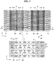
- FIG. 3 illustrates an example of a string applied to a solar cell module according to an embodiment of the invention when viewed from a back surface.
- Each of a plurality of solar cells C1 and C2 may at least include a semiconductor substrate 110 and a plurality of first and second electrodes C141 and C142 that are spaced apart from each other on a surface (for example, a back surface) of the semiconductor substrate 110 and extend in the first direction x.
- a plurality of conductive lines CW may electrically connect in series a plurality of first electrodes C141 included in one solar cell of two adjacent solar cells among the plurality of solar cells to a plurality of second electrodes C142 included in the other solar cell through an interconnector IC.
- the plurality of conductive lines CW may extend in the second direction y crossing a longitudinal direction (i.e., the first direction x) of the first and second electrodes C141 and C142 and may be connected to each of the plurality of solar cells.
- the plurality of conductive lines CW may include a plurality of first conductive lines CW1 and a plurality of second conductive lines CW2.
- the first conductive line CW1 may be connected to the first electrode C141 included in each solar cell using a conductive adhesive CA and may be insulated from the second electrode C142 of each solar cell through an insulating layer IL formed of an insulating material.
- the second conductive line CW2 may be connected to the second electrode C142 included in each solar cell using a conductive adhesive CA and may be insulated from the first electrode C141 of each solar cell through an insulating layer IL formed of an insulating material.
- a linewidth WCW of each conductive line CW may be 0.5 mm to 2.5 mm in consideration of a reduction in the manufacturing cost while maintaining a line resistance of the conductive line CW at a sufficiently low level.
- a distance WDCW between the first and second conductive lines CW1 and CW2 may be 4 mm to 6.5 mm in consideration of the total number of conductive lines CW, so that a short circuit current of the solar cell module is not damaged.
- a thickness of each conductive line CW may be 0.05 mm to 0.3 mm.
- the interconnector IC may be positioned between the first and second solar cells C1 and C2 and may extend in the first direction x.
- the first and second conductive lines CW1 and CW2 may be connected to the interconnector IC, and thus the plurality of solar cells may be connected in series in the second direction y.
- the embodiment of the invention is illustrated and described using an example where the solar cell module according to the embodiment of the invention includes the interconnector IC.
- the interconnector IC may be omitted.
- the first and second conductive lines CW1 and CW2 may be directly connected to each other or may be formed as one body, thereby connecting the plurality solar cells C1 and C2 in series.
- An insulating adhesive portion AT may extend in the first direction x on at least a portion of a surface (for example, the back surface) of the semiconductor substrate 110, on which the conductive lines CW are disposed.
- the insulating adhesive portion AT may serve to fix (or temporality fix) the conductive lines CW to the semiconductor substrate 110 and to the first and second electrodes C141 and C142 during a process for manufacturing the solar cell module.
- the insulating adhesive portion AT may serve to temporarily fix the conductive lines CW to a surface (for example, the back surface) of the semiconductor substrate 110, so that the conductive lines CW disposed on the surface (for example, the back surface) of the semiconductor substrate 110 do not move on the surface (for example, the back surface) of the semiconductor substrate 110.
- the insulating adhesive portion AT may be disposed around a middle portion and both edges of the semiconductor substrate 110 and may extend in the first direction x crossing a longitudinal direction of the conductive lines CW.
- the insulating adhesive portion AT can make it easier to perform the manufacturing process of the solar cell module by fixing the conductive lines CW disposed on the back surface of the semiconductor substrate 110 so that the conductive lines CW do not move before the tabbing process.
- the insulating adhesive portion AT may be attached to a back surface of a portion of each conductive line CW and the back surface of the semiconductor substrate 110 and may temporarily fix a portion of each conductive line CW to the back surface of the semiconductor substrate 110.
- the insulating adhesive portion AT may be melted during the lamination process for modularizing the plurality of solar cells and may be adhered and attached up to a side as well as a back surface of a portion of each conductive line CW in the solar cell module, that has been finally completed.
- the conductive line CW When the insulating adhesive portion AT is adhered and attached up to the side as well as the back surface of at least a portion of each conductive line CW as described above, the conductive line CW, to which the insulating adhesive portion AT is attached, may minimize a formation space of an air trap at a side of the conductive line CW. Hence, the conductive line CW can be prevented from being corroded by moisture contained in the air trap.
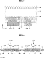
- FIG. 4 is a partial perspective view illustrating an example of a solar cell applied to a solar cell module shown in FIG. 3 .
- FIG. 5 is a cross-sectional view of a solar cell shown in FIG. 4 in a second direction.
- an example of a solar cell may include an anti-reflection layer 130, a semiconductor substrate 110, a tunnel layer 180, a plurality of emitter regions 121, a plurality of back surface field regions 172, a plurality of intrinsic semiconductor layers 150, a passivation layer 190, a plurality of first electrodes C141, and a plurality of second electrodes C142.
- the anti-reflection layer 130, the intrinsic semiconductor layer 150, the tunnel layer 180, and the passivation layer 190 may be omitted, if desired or necessary.
- efficiency of the solar cell may be further improved.
- the embodiment of the invention is described using the solar cell including the anti-reflection layer 130, the intrinsic semiconductor layer 150, the tunnel layer 180, and the passivation layer 190 by way of example.
- the semiconductor substrate 110 may be formed of at least one of single crystal silicon and polycrystalline silicon containing impurities of a first conductive type.
- the semiconductor substrate 110 may be formed of a single crystal silicon wafer.
- the first conductive type may be one of an n-type and a p-type.
- the semiconductor substrate 110 When the semiconductor substrate 110 is of the p-type, the semiconductor substrate 110 may be doped with impurities of a group III element, such as boron (B), gallium (Ga), and indium (In).
- a group III element such as boron (B), gallium (Ga), and indium (In).
- the semiconductor substrate 110 when the semiconductor substrate 110 is of the n-type, the semiconductor substrate 110 may be doped with impurities of a group V element, such as phosphorus (P), arsenic (As), and antimony (Sb).
- the embodiment of the invention is described using an example where the first conductive type is the n-type.
- a front surface of the semiconductor substrate 110 may be an uneven surface having a plurality of uneven portions or having uneven characteristics.
- the emitter regions 121 positioned on the front surface of the semiconductor substrate 110 may have an uneven surface.
- an amount of light reflected from the front surface of the semiconductor substrate 110 may decrease, and an amount of light incident on the inside of the semiconductor substrate 110 may increase.
- the anti-reflection layer 130 may be positioned on the front surface of the semiconductor substrate 110, so as to minimize a reflection of light incident on the front surface of the semiconductor substrate 110 from the outside.
- the anti-reflection layer 130 may be formed of at least one of aluminum oxide (AlOx), silicon nitride (SiNx), silicon oxide (SiOx), and silicon oxynitride (SiOxNy).
- the tunnel layer 180 is disposed on an entire back surface of the semiconductor substrate 110 while directly contacting the entire back surface of the semiconductor substrate 110 and may include a dielectric material. Thus, as shown in FIGS. 4 and 5 , the tunnel layer 180 may pass through carriers produced in the semiconductor substrate 110.
- the tunnel layer 180 may pass through carriers produced in the semiconductor substrate 110 and may perform a passivation function with respect to the back surface of the semiconductor substrate 110.
- the tunnel layer 180 may be formed of a dielectric material including silicon carbide (SiCx) or silicon oxide (SiOx) having strong durability at a high temperature equal to or higher than 600 °C. Other materials may be used.
- the tunnel layer 180 may be formed of silicon nitride (SiNx), hydrogenated SiNx, aluminum oxide (AlOx), silicon oxynitride (SiON), or hydrogenated SiON.
- a thickness of the tunnel layer 180 may be 0.5 nm to 2.5 nm.
- the plurality of emitter regions 121 may be disposed on the back surface of the semiconductor substrate 110, and more specifically may directly contact a portion of a back surface of the tunnel layer 180.
- the plurality of emitter regions 121 may extend in the first direction x.
- the emitter regions 121 may be formed of polycrystalline silicon material of a second conductive type opposite the first conductive type.
- the emitter regions 121 may form a p-n junction together with the semiconductor substrate 110 with the tunnel layer 180 interposed therebetween.
- each emitter region 121 forms the p-n junction together with the semiconductor substrate 110, the emitter region 121 may be of the p-type. However, if the semiconductor substrate 110 is of the p-type unlike the embodiment described above, the emitter region 121 may be of the n-type. In this instance, separated electrons may move to the plurality of emitter regions 121, and separated holes may move to the plurality of back surface field regions 172.
- the plurality of back surface field regions 172 may be disposed on the back surface of the semiconductor substrate 110. More specifically, the plurality of back surface field regions 172 may directly contact a portion (spaced apart from each of the plurality of emitter regions 121) of the back surface of the tunnel layer 180. The plurality of back surface field regions 172 may extend in the first direction x parallel to the plurality of emitter regions 121.
- a potential barrier is formed by a difference between impurity concentrations of the semiconductor substrate 110 and the back surface field regions 172.
- the back surface field regions 172 can prevent or reduce holes from moving to the back surface field regions 172 used as a moving path of electrons through the potential barrier and can make it easier for carriers (for example, electrons) to move to the back surface field regions 172.
- the embodiment of the invention can reduce an amount of carriers lost by a recombination and/or a disappearance of electrons and holes at and around the back surface field regions 172 or at and around the first and second electrodes C141 and C142 and can accelerate a movement of electrons, thereby increasing an amount of electrons moving to the back surface field regions 172.
- FIGS. 4 and 5 illustrate that the emitter regions 121 and the back surface field regions 172 are formed on the back surface of the tunnel layer 180 using polycrystalline silicon material, by way of example.
- the emitter regions 121 and the back surface field regions 172 may be doped by diffusing impurities into the back surface of the semiconductor substrate 110.
- the emitter regions 121 and the back surface field regions 172 may be formed of the same material (for example, single crystal silicon) as the semiconductor substrate 110.
- the intrinsic semiconductor layer 150 may be formed on the back surface of the tunnel layer 180 exposed between the emitter region 121 and the back surface field region 172.
- the intrinsic semiconductor layer 150 may be formed as an intrinsic polycrystalline silicon layer, that is not doped with impurities of the first conductive type or impurities of the second conductive type, unlike the emitter region 121 and the back surface field region 172.
- the passivation layer 190 removes a defect resulting from a dangling bond formed in a back surface of a polycrystalline silicon layer formed at the back surface field regions 172, the intrinsic semiconductor layers 150, and the emitter regions 121, and thus can prevent carriers produced in the semiconductor substrate 110 from being recombined and disappeared by the dangling bond.
- the passivation layer 190 may cover a remaining portion except a portion, on which the first and second electrodes C141 and C142 are formed, from the back surface of the semiconductor substrate 110.
- the passivation layer 190 may be formed of a dielectric material.
- the passivation layer 190 may be formed of at least one of hydrogenated silicon nitride (SiNx:H), hydrogenated silicon oxide (SiOx:H), hydrogenated silicon nitride oxide (SiNxOy:H), hydrogenated silicon oxynitride (SiOxNy:H), and hydrogenated amorphous silicon (a-Si:H).
- the first electrode C141 may be connected to the emitter region 121 and may extend in the first direction x.
- the first electrode C141 may collect carriers (for example, holes) moving to the emitter region 121.
- the second electrode C142 may be connected to the back surface field region 172 and may extend in the first direction x in parallel with the first electrode C141.
- the second electrode C142 may collect carriers (for example, electrons) moving to the back surface field region 172.
- the first and second electrodes C141 and C142 may extend in the first direction x and may be alternately disposed in the second direction y.
- the first and second electrodes C141 and C142 may include a metal material different from conductive lines CW and a conductive adhesive CA.
- each of the first and second electrodes C141 and C142 may be formed as at least one layer including at least one of titanium (Ti), silver (Ag), aluminum (Al), nickel-vanadium (NiV) alloy, nickel (Ni), nickel-aluminum (NixAly) alloy, molybdenum (Mo), or tin (Sn).
- holes collected by the first electrodes C141 and electrons collected by the second electrodes C142 may be used as electric power of an external device through an external circuit device.
- the solar cell applied to the solar cell module according to the embodiment of the invention is not limited to FIGS. 4 and 5 .
- the components of the solar cell may be variously changed, except that the first and second electrodes C141 and C142 included in the solar cell are formed on the back surface of the semiconductor substrate 110.
- the solar cell module according to the embodiment of the invention may use a metal wrap through (MWT) solar cell, that is configured such that a portion of the first electrode C141 and the emitter region 121 are positioned on the front surface of the semiconductor substrate 110, and the portion of the first electrode C141 is connected to a remaining portion of the first electrode C141 formed on the back surface of the semiconductor substrate 110 through a hole of the semiconductor substrate 110.
- MTT metal wrap through
- FIG. 6 illustrates a cross-sectional structure, in which the plurality of solar cells each having above-described configuration are connected in series using the conductive lines CW and the interconnector IC as shown in FIG. 3 .
- FIG. 6 is a cross-sectional view taken along line csx1-csx1 of FIG. 3 .
- the first and second solar cells C1 and C2, that are arranged in the second direction y as described above, may be connected in series to each other in the second direction y using first and second conductive lines CW1 and CW2 and an interconnector IC to form a string.
- the first and second conductive lines CW1 and CW2 and the interconnector IC may be formed of a conductive metal material.
- the first and second conductive lines CW1 and CW2 may be connected to the back surface of the semiconductor substrate 110 of each solar cell and then may be connected to the interconnector IC for a serial connection of the solar cells.
- the plurality of first conductive lines CW1 may overlap the plurality of first electrodes C141 included in each of the first and second solar cells C1 and C2 and may be connected to the plurality of first electrodes C141 through a conductive adhesive CA. Further, the plurality of first conductive lines CW1 may be insulated from the plurality of second electrodes C142 included in each of the first and second solar cells C1 and C2 through an insulating layer IL formed of an insulating material.
- each of the plurality of first conductive lines CW1 may protrude to the outside of the semiconductor substrate 110 toward the interconnector IC disposed between the first and second solar cells C1 and C2.
- the conductive adhesive CA may be formed of a metal material including tin (Sn) or Sn-containing alloy.
- the conductive adhesive CA may be formed as one of a solder paste including Sn or Sn-containing alloy, an epoxy solder paste, in which Sn or Sn-containing alloy is included in an epoxy, and a conductive paste.
- the solder paste may include at least one metal material of Sn, SnBi, SnIn, SnAgCu, SnPb, SnBiCuCo, SnBiAg, SnPbAg, or SnAg.
- the epoxy solder paste may be formed by including at least one metal material of Sn, SnBi, SnIn, SnAgCu, SnPb, SnBiCuCo, SnBiAg, SnPbAg, or SnAg in an epoxy resin.
- the conductive paste may be formed by including at least one metal material of Sn, SnBi, Ag, AgIn, or AgCu in a resin, for example, an epoxy.
- the insulating layer IL may be made of any material as long as an insulating material is used.
- the insulating layer IL may use one insulating material of an epoxy-based resin, polyimide, polyethylene, an acrylic-based resin, and a silicon-based resin.
- the conductive adhesive CA may be positioned only on the back surface of the first electrode or the second electrode positioned in a portion crossing the conductive line CW.
- the insulating layer IL may be positioned not only on the back surface of the first electrode or the second electrode positioned in a portion crossing the conductive line CW but also on the back surface of the semiconductor substrate 110 around the back surface of the first electrode or the second electrode.
- a portion protruding to the outside of the semiconductor substrate 110 in each of the first and second conductive lines CW1 and CW2 connected to the back surface of each solar cell may be commonly connected to the back surface of the interconnector IC between the first and second solar cells C1 and C2.
- the plurality of solar cells C1 and C2 may be connected in series to each other in the second direction y to form a string.
- the first and second conductive lines CW1 and CW2 of a solar cell having the bad connection may be disconnected from the interconnector IC. Hence, only the bad solar cell can be easily replaced.
- a structure of the insulating adhesive portion AT attached to the back surface of the semiconductor substrate 110 is described in detail below.
- FIGS. 7 to 9 illustrate in detail a structure of an insulating adhesive portion AT illustrated in FIGS. 3 and 6 .
- FIG. 7 is an enlarged view of a back surface of a solar cell module, to which an insulating adhesive portion AT is attached as shown in FIG. 3 .
- FIG. 8 (a) is an enlarged view of a cross section of the second direction along line A-A of FIG. 7 before a lamination step, and in FIG. 8 , (b) is an enlarged view of a cross section of the second direction along line A-A of FIG. 7 in a finally completed solar cell module after the lamination step.
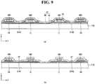
- FIG. 9 (a) is an enlarged view of a cross section of the first direction along line B-B of FIG. 7 before a lamination step, and in FIG. 9 , (b) is an enlarged view of a cross section of the first direction along line B-B of FIG. 7 in a finally completed solar cell module after the lamination step.
- FIGS. 7 to 9 The description duplicative with that illustrated in FIGS. 3 to 6 is omitted in FIGS. 7 to 9 , and only a difference between FIGS. 3 to 6 and FIGS. 7 to 9 is mainly described.
- a width WYAT of the insulating adhesive portion AT in the second direction y may be greater than a distance WDCW between the two adjacent conductive lines CW and may be less than five times the distance WDCW, in order to further increase an adhesive strength of the insulating adhesive portion AT.
- the width WYAT of the insulating adhesive portion AT in the second direction y may be, for example, 2.5 mm to 30 mm in consideration of a physical adhesive strength of the insulating adhesive portion AT for fixing the conductive line CW.
- the width WYAT may be 5 mm to 15 mm.
- FIG. 3 illustrates that a length of the insulating adhesive portion AT in the first direction x is slightly shorter than a length of the semiconductor substrate 110 in the first direction x. However, they may be substantially the same as each other.
- the length of the insulating adhesive portion AT in the first direction x may be changed depending on a size of the semiconductor substrate 110.
- the length of the insulating adhesive portion AT in the first direction x may be 156 mm to 162 mm.
- the plurality of first and second electrodes C141 and C142 extending in the first direction x may overlap one insulating adhesive portion AT.
- the insulating adhesive portion AT may be a type of an insulating tape obtained by forming an adhesive IA on a surface of a base film BF.
- the base film BF may melt during the lamination process because a melting point of the base film BF is lower than a temperature of the lamination process for modularizing the plurality of solar cells.
- the base film BF may include polyolefin capable of melting during the lamination process.
- the fact that the base film BF melts during the lamination process means that the base film BF is not fully burned but softened in a paste state having a viscosity.
- the melting point of the base film BF may be lower than one temperature between 160 °C and 170 °C, for example.
- the adhesive IA of the insulating adhesive portion AT may include at least one of acrylic, silicon, or an epoxy.
- the adhesive IA may melt during the lamination process.
- the insulating adhesive portion AT when the insulating adhesive portion AT attaches the conductive lines CW1 and CW2 to the back surface of the semiconductor substrate 110 before the lamination process for modularizing the plurality of solar cells, the insulating adhesive portion AT may be attached to the back surfaces of the conductive lines CW1 and CW2 disposed on the back surface of the semiconductor substrate 110, to the back surface of the semiconductor substrate 110 exposed between the conductive lines CW1 and CW2, and to the back surfaces of the first and second electrodes C141 and C142.
- the base film BF and the adhesive IA of the insulating adhesive portion AT may melt and may be filled in the sides of the conductive lines CW1 and CW2, in a space between the conductive lines CW1 and CW2 and the insulating layer IL, and in a space between the conductive lines CW1 and CW2 and the back surface of the semiconductor substrate 110. Then, the insulating adhesive portion AT in a state filled in the above-described locations may be dried and cured.
- the insulating adhesive portion AT may be adhered and attached up to the sides of the conductive lines CW1 and CW2 and a space between the conductive lines CW1 and CW2 and the insulating layer IL in the finally completed solar cell module.
- the solar cell module according to the embodiment of the invention can minimize the generation of the air trap at the sides and the periphery of the conductive lines CW1 and CW2 and prevent the conductive lines CW1 and CW2 from being corroded by moisture.
- an empty space ES may be formed by a height difference between the back surface of the conductive line CW and the back surface of the semiconductor substrate 110.
- the empty space ES may be surrounded by the sides of the conductive lines CW1 and CW2, the insulating adhesive portion AT, and the back surface of the semiconductor substrate 110.
- Air may be naturally filled in the empty space ES during a manufacturing process of the solar cell module. If the empty space ES is not removed and remains in the finally completed solar cell module, the air may be confined in the empty space ES and the empty space may be sealed. Hence, the air trap may be formed.
- the solar cell module when used in an outdoor space afterward, moisture may be contained in the air trap due to an outdoor weather environment.
- the conductive lines CW1 and CW2 may be corroded, and a resistance of the conductive lines CW1 and CW2 may increase.
- the insulating adhesive portion AT includes a material capable of melting during the lamination process as described above, the insulating adhesive portion AT may melt and may be filled in the empty space ES surrounded by the sides of the conductive lines CW1 and CW2, the insulating adhesive portion AT, and the back surface of the semiconductor substrate 110. Hence, the insulating adhesive portion AT can prevent the formation of the air trap and prevent a reduction in the efficiency of the solar cell module.
- the embodiment of the invention described the use of polyolefin as an example of the material of the insulating adhesive portion AT capable of melting during the lamination process, but is not limited thereto. Any material may be used for the insulating adhesive portion AT as long as the material melts in the lamination process performed at one temperature between 160 °C and 170 °C.
- the insulating adhesive portion AT may be transparent, but may be white or black.
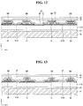
- FIGS. 10 to 13 illustrate a method for manufacturing a solar cell module according to the embodiment of the invention.
- a method for manufacturing a solar cell module according to the embodiment of the invention is described in detail below with reference to FIGS. 7 to 9 together with FIG. 10 .
- a method for manufacturing a solar cell module includes a conductive adhesive application operation S1, a conductive line disposition operation S2, an insulating adhesive portion attaching operation S3, and a lamination operation S4.
- the solar cell may be a back contact solar cell, in which all of the first and second electrodes C141 and C142 are disposed on a back surface of the semiconductor substrate 110.
- the embodiment of the invention is not limited to the back contact solar cell.
- the embodiment of the invention may use a conventional solar cell, in which the first electrodes C141 are disposed on a front surface of the semiconductor substrate 110 and the second electrodes C142 are disposed on the back surface of the semiconductor substrate 110.
- a conductive adhesive CA may be applied to a portion of each of the first and second electrodes C141 and C142 in the conductive adhesive application operation S1.
- a portion of each of the first and second electrodes C141 and C142, to which the conductive adhesive CA is applied, may be a crossing portion of conductive lines CW and the first and second electrodes C141 and C142.
- An insulating layer IL may be additionally formed in a portion of the conductive line CW that has to be insulated from the first electrode C141 or the second electrode C142.
- the conductive adhesive CA may be applied to a crossing portion of the first electrode C141 and the first conductive line CW1 and a crossing portion of the second electrode C142 and the second conductive line CW2 in the back surface of the semiconductor substrate 110 and may be dried.
- the insulating layer IL may be formed in a crossing portion of the first electrode C141 and the second conductive line CW2 and a crossing portion of the second electrode C142 and the first conductive line CW1 and may be cured.
- a thickness of the insulating layer IL may be less than a thickness of the conductive adhesive CA, in order to more certainly secure a connection strength between the conductive adhesive CA and the conductive line CW.
- the conductive lines CW may be disposed to extend in a second direction y crossing the first direction x, so that the conductive lines CW overlap a portion of each of the first and second electrodes C141 and C142, to which the conductive adhesive CA is applied.
- all of the conductive lines CW may be disposed on the back surface of the semiconductor substrate 110.
- a disposition structure of the conductive adhesive CA, the insulating layer IL, and the conductive lines CW formed on the first and second electrodes C141 and C142 may be the same as FIG. 3 .
- the conductive line CW may not be attached to the back surface of the semiconductor substrate 110.
- an insulating adhesive portion AT extending in the first direction x may be attached to a portion of the back surface of the semiconductor substrate 110 and a portion of the conductive lines CW disposed on the portion of the back surface of the semiconductor substrate 110, in order to easily perform the manufacturing process.
- the insulating adhesive portion AT may fix the conductive lines CW disposed on the back surface of the semiconductor substrate 110 to the back surface of the semiconductor substrate 110.
- a melting point of the insulating adhesive portion AT may be lower than a temperature of the lamination operation S4. More specifically, as shown in (a) of FIG. 8 and (a) of FIG. 9 , the insulating adhesive portion AT may be a type of an insulating tape obtained by forming an adhesive IA on a surface of a base film BF. Melting points of the base film BF and the adhesive IA may be lower than the temperature of the lamination operation S4.
- the melting points of the base film BF and the adhesive IA may be lower than the one temperature between 160 °C and 170 °C.
- the base film BF may include a polyolefin material, of which a melting point is lower than the temperature of the lamination operation S4.
- the adhesive IA may include at least one of acrylic, silicon, or an epoxy, of which a melting point is lower than the temperature of the lamination operation S4.
- each solar cell may be disposed on a front transparent substrate 10.
- a front encapsulant 20 may be disposed on the front transparent substrate 10, and an interconnector IC may be disposed on the front encapsulant 20.
- the solar cell, to which the insulating adhesive portion AT is attached may be disposed on the front encapsulant 20.
- Ends of the conductive lines CW fixed to each solar cell may overlap the interconnector IC.
- a back encapsulant 30 and a back substrate 40 may be sequentially disposed on the back surface of the semiconductor substrate 110, to which the insulating adhesive portion AT is attached.
- the lamination operation S4 involving heat and pressure may be performed in a state where the plurality of solar cells are disposed between the front transparent substrate 10 and the back substrate 40.
- the lamination operation S4 may be performed at one temperature between 160 °C and 170 °C.
- the lamination operation S4 may be performed at 165 °C.
- the insulating adhesive portion AT may extend from a portion of the conductive line CW to a side of the conductive line CW in a state where the insulating adhesive portion AT is softened in a paste form having a viscosity through a thermal process of the lamination operation S4.
- the insulating adhesive portion AT may extend to an empty space ES between the conductive lines CW and the first and second electrodes C141 and C142 (or an empty space ES between the conductive lines CW and the insulating layer IL) in a softened state of the insulating adhesive portion AT.
- the insulating adhesive portion AT extended to the empty space ES may be cured.
- the back encapsulant 30 of a sheet shape may be softened together with the insulating adhesive portion AT and may be filled in an empty space between the insulating adhesive portion AT and the back encapsulant 30.
- the method for manufacturing the solar cell module according to the embodiment of the invention fixes the conductive lines CW to the back surface of the semiconductor substrate 110 through the insulating adhesive portion AT in a state where the conductive lines CW are disposed on the back surface of the semiconductor substrate 110, the lamination operation S4 can be more easily performed.
- the embodiment of the invention cures the insulating adhesive portion AT in a state where the insulating adhesive portion AT is softened and filled in an empty space ES between the conductive lines CW and the first and second electrodes C141 and C142 or an empty space ES between the conductive lines CW and the semiconductor substrate 110 in the lamination operation S4, thereby minimizing the generation of the air trap in the completed solar cell module.
- the conductive lines CW can be prevented from being corroded by moisture.
- the conductive lines CW fixed to each solar cell may be electrically connected to the interconnector IC. However, this is not necessarily performed. For example, after the insulating adhesive portion AT fixes the conductive lines CW to the back surface of the semiconductor substrate 110, the conductive lines CW fixed to each solar cell may be electrically connected to the interconnector IC through a separate thermal process before the lamination operation S4.
- the method for manufacturing the solar cell module according to the embodiment of the invention was described using the back contact solar cell by way of example.
- the conventional solar cell may be used.
- a process for forming the insulating layer IL may be omitted in the conductive adhesive application operation S1. Further, in the conductive line disposition operation S2, a portion of the conductive line CW may be disposed on the front surface of the semiconductor substrate 110, and a remaining portion of the conductive line CW may be disposed on the back surface of the semiconductor substrate 110.
Landscapes
- Photovoltaic Devices (AREA)
- Life Sciences & Earth Sciences (AREA)
- Engineering & Computer Science (AREA)
- Sustainable Energy (AREA)
- Sustainable Development (AREA)
- Electroluminescent Light Sources (AREA)
- Manufacturing & Machinery (AREA)
Description
- Embodiments of the invention relate to a solar cell module and a method for manufacturing the same.
- Recently, as existing energy sources such as petroleum and coal are expected to be depleted, interests in alternative energy sources for replacing the existing energy sources are increasing. Among the alternative energy sources, solar cells for generating electric energy from solar energy have been particularly spotlighted.
- A solar cell generally includes semiconductor parts, which respectively have different conductive types, for example, a p-type and an n-type and thus form a p-n junction, and electrodes respectively connected to the semiconductor parts of the different conductive types.
- When light is incident on the solar cell, a plurality of electron-hole pairs are produced in the semiconductor parts and are separated into electrons and holes by the incident light. The electrons move to the n-type semiconductor part, and the holes move to the p-type semiconductor part. Then, the electrons and the holes are collected by the different electrodes respectively connected to the n-type semiconductor part and the p-type semiconductor part. The electrodes are connected to each other using electric wires to thereby obtain electric power.
- A plurality of solar cells having the above-described configuration may be connected to one another through interconnectors to form a module.
- A back contact solar cell is a solar cell, in which all of electrodes are disposed on a back surface of a semiconductor substrate. A plurality of back contact solar cells may be connected in series to one another through a plurality of conductive lines connected to a back surface of a semiconductor substrate of each back contact solar cell.
- In such a structure in which a plurality of conductive lines are connected to a back surface of a semiconductor substrate, before the conductive lines are connected to the back surface of the semiconductor substrate, the plurality of conductive lines, that are disposed on the back surface of the semiconductor substrate and are not fixed to the back surface of the semiconductor substrate, may move on the back surface of the semiconductor substrate and may be out of alignment. Hence, there is a difficulty in a module manufacturing process.
-
EP 2 983 212 A1 discloses a solar cell module including a plurality of solar cells, each of which includes a semiconductor substrate and first and second electrode parts each having a different polarity, a plurality of interconnectors for electrically connecting the plurality of solar cells, a conductive adhesive for electrically connecting each of the plurality of interconnectors to the corresponding electrode part of each of the plurality of solar cells, and at least one insulating adhesive portion for temporarily fixing the plurality of interconnectors to the corresponding electrode part. The at least one insulating adhesive portion includes an adhesive having adhesiveness to attach the interconnector to the corresponding electrode part at the room temperature. - In one aspect, there is provided a solar cell module including solar cells each including a semiconductor substrate, and first electrodes and second electrodes that extend in a first direction on a surface of the semiconductor substrate, the first electrodes and the second electrodes having different polarities, conductive lines extended in a second direction crossing the first direction on the surface of the semiconductor substrate, the conductive lines being connected to the first electrodes or the second electrodes through a conductive adhesive, and an insulating adhesive portion extending in the first direction on at least a portion of the surface of the semiconductor substrate, on which the conductive lines are disposed, and fixing the conductive lines to the semiconductor substrate and the first and second electrodes, the insulating adhesive portion being attached on a back surface of least a portion of each conductive line and a side surface of at least a portion of each conductive line. The insulating adhesive portion overlaps a portion of each conductive line and a plurality of the electrodes.
- The insulating adhesive portion may be further attached up to the semiconductor substrate exposed between the conductive lines and surfaces of the first and second electrodes.
- The insulating adhesive portion may be an insulating tape including an adhesive on a surface of a base film. The base film may include a polyolefin material. A melting point of the base film may be lower than one temperature between 160 °C and 170 °C.
- The adhesive of the insulating adhesive portion may include at least one of acrylic, silicon, and an epoxy.
- A width of the insulating adhesive portion in the second direction may be greater than a distance between two adjacent conductive lines.
- The first electrodes and the second electrodes may be positioned on a back surface of the semiconductor substrate. The conductive lines may be positioned on the back surface of the semiconductor substrate, on which the first electrodes and the second electrodes are positioned.
- The insulating adhesive portion may be positioned on the back surface of the semiconductor substrate, on which the first electrodes, the second electrodes, and the conductive lines are positioned.
- The semiconductor substrate of each solar cell may be doped with impurities of a first conductive type. Each solar cell may further include an emitter region doped with impurities of a second conductive type opposite the first conductive type at the back surface of the semiconductor substrate and a back surface field region more heavily doped than the semiconductor substrate with impurities of the first conductive type.
- Each first electrode may be connected to the emitter region, and each second electrode may be connected to the back surface field region.
- The conductive lines may include first conductive lines connected to the first electrodes through the conductive adhesive and insulated from the second electrodes through an insulating layer, and second conductive lines connected to the second electrodes through the conductive adhesive and insulated from the first electrodes through the insulating layer.
- The solar cells may include a first solar cell and a second solar cell that are arranged adjacent to each other in the second direction and are connected in series to each other. An interconnector may be positioned between the first solar cell and the second solar cell and connects the first solar cell and the second solar cell in series.
- The interconnector between the first solar cell and the second solar cell may extend in the first direction. The first conductive lines connected to the first solar cell and the second conductive lines connected to the second solar cell may be commonly connected to the interconnector.
- In another aspect, there is provided a method for manufacturing a solar cell module, the method including applying a conductive adhesive to a portion of each of first electrodes and the second electrodes, the first electrodes and the second electrodes extending in a first direction on a surface of a semiconductor substrate and having different polarities, disposing conductive lines to extend in a second direction crossing the first direction and to overlap the portion of the each of the first electrodes and the second electrodes, to which the conductive adhesive is applied, attaching an insulating adhesive portion extending in the first direction to the semiconductor substrate so that the insulting adhesive portion overlaps a portion of each conductive line and a plurality of the electrodes, and performing a lamination process on the semiconductor substrate, to which the insulating adhesive portion is attached, wherein the performing of the lamination process includes softening and curing the insulating adhesive portion, the insulating adhesive portion is attached on a back surface of at least the portion of each conductive line in the attaching of the insulating adhesive portion, and the insulating adhesive portion is further attached on a side surface of the at least the portion of the each conductive line while the insulating adhesive portion is softened and cured.
- The lamination process may be performed at one temperature between 160 °C and 170 °C.
- A melting point of the insulating adhesive portion may be lower than a temperature of the lamination process. The insulating adhesive portion may be a type of an insulating tape obtained by forming an adhesive on a surface of a base film.
- The base film may include a polyolefin material, and melting points of the base film and the adhesive may be lower than a temperature of the lamination process.
- The performing of the lamination process may include filling the insulating adhesive portion, that is in a softened state, in at least a portion of an empty space between the conductive lines and the first electrodes and the second electrodes and then curing the insulating adhesive portion.
- The accompanying drawings, which are included to provide a further understanding of the invention and are incorporated in and constitute a part of this specification, illustrate embodiments of the invention and together with the description serve to explain the principles of the invention. In the drawings:
-
FIG. 1 is a plane view of an entire front surface of a solar cell module according to an embodiment of the invention; -
FIG. 2 schematically illustrates a cross section of a string, in which first and second solar cells are connected by an interconnector; -
FIG. 3 illustrates a back surface of a string, in which first and second solar cells are connected by an interconnector; -
FIG. 4 is a partial perspective view illustrating an example of a solar cell shown inFIG. 3 ; -
FIG. 5 is a cross-sectional view of a solar cell shown inFIG. 4 in a second direction; -
FIG. 6 is a cross-sectional view taken along line csx1-csx1 ofFIG. 3 ; -
FIG. 7 is an enlarged view of a back surface of a solar cell module, to which an insulating adhesive portion shown inFIG. 3 is attached; - In
FIG. 8 , (a) is an enlarged view of a cross section of a second direction along line A-A ofFIG. 7 before a lamination step, and inFIG. 8 , (b) is an enlarged view of a cross section of the second direction along line A-A ofFIG. 7 in a finally completed solar cell module after the lamination step; - In
FIG. 9 , (a) is an enlarged view of a cross section of a first direction along line B-B ofFIG. 7 before a lamination step, and inFIG. 9 , (b) is an enlarged view of a cross section of the first direction along line B-B ofFIG. 7 in a finally completed solar cell module after the lamination step; and -
FIGS. 10 to 13 illustrate a method for manufacturing a solar cell module according to an embodiment of the invention. - Reference will now be made in detail to embodiments of the invention, examples of which are illustrated in the accompanying drawings. This invention may, however, be embodied in many different forms and should not be construed as limited to the embodiments set forth herein. Wherever possible, the same reference numbers will be used throughout the drawings to refer to the same or like parts. It will be noted that a detailed description of known arts will be omitted if it is determined that the detailed description of the known arts can obscure the embodiments of the invention.
- In the drawings, the thickness of layers, films, panels, regions, etc., are exaggerated for clarity. It will be understood that when an element such as a layer, film, region, or substrate is referred to as being "on" another element, it can be directly on the other element or intervening elements may also be present. In contrast, when an element is referred to as being "directly on" another element, there are no intervening elements present. Further, it will be understood that when an element such as a layer, film, region, or substrate is referred to as being "entirely" on other element, it may be on the entire surface of the other element and may not be on a portion of an edge of the other element.
- In the following description, a front surface of any component may be a surface of a direction facing a front surface of a module, on which light is directly incident, and a back surface of any component may be a surface of a direction facing a back surface of the module, on which light is not directly incident or reflective light may be incident.
- In the following description, a cell string indicates a structure or a shape, in which a plurality of solar cells are connected in series to one another
- In the following description, the fact that a thickness or a width of a component is equal to a thickness or a width of another component indicates that they have the same value within a margin of error of 10 % including a process error.
-
FIG. 1 is a plane view of an entire front surface of a solar cell module according to an embodiment of the invention.FIG. 2 schematically illustrates a cross section of first and second solar cells that are adjacent to each other in a second direction and are connected by an interconnector. - As shown in
FIGS. 1 and2 , a solar cell module according to an embodiment of the invention may include a plurality of solar cells C1 and C2, a plurality of conductive lines CW, an insulating adhesive portion AT, and an interconnector IC. - In the embodiment disclosed herein, the interconnector IC may be omitted, if necessary or desired. However, the embodiment of the invention is described using the solar cell module including the interconnector IC by way of example as shown in
FIG. 1 . - The solar cell module according to the embodiment of the invention may further include components (for example, a front
transparent substrate 10,encapsulants back substrate 40, and a frame 50) for encapsulating a cell string formed by connecting the plurality of solar cells C1 and C2 in series. - As shown in
FIG. 1 , each solar cell may be arranged to extend in a second direction y and may include asemiconductor substrate 110 and a plurality of first and second electrodes C141 and C142 on a back surface of thesemiconductor substrate 110. - As shown in
FIGS. 1 and2 , a plurality of first and second conductive lines CW may be connected to a back surface of each solar cell. - As shown in
FIGS. 1 and2 , the plurality of solar cells, to which the plurality of first and second conductive lines CW are connected, may be connected in series to each other in the second direction y by the interconnector IC. - For example, the interconnector IC may be disposed to extend between two adjacent solar cells in a first direction x and may connect in series first and second solar cells C1 and C2, that are spaced apart from each other in the second direction y among the plurality of solar cells.
- In this instance, as shown in
FIG. 2 , front surfaces of a plurality of first conductive lines CW1 connected to the first solar cell C1 and front surfaces of a plurality of second conductive lines CW2 connected to the second solar cell C2 may be connected to a back surface of the interconnector IC. Hence, the plurality of solar cells C1 and C2 may be connected in series to form a cell string. - As shown in
FIG. 2 , the cell string, that is disposed between the fronttransparent substrate 10 and theback substrate 40, may be thermally pressed and laminated. - For example, a lamination process simultaneously applying heat and pressure may be performed in a state where the plurality of solar cells C1 and C2 are disposed between the front
transparent substrate 10 and theback substrate 40, and theencapsulants - As shown in
FIG. 1 , edges of the fronttransparent substrate 10, theencapsulants back substrate 40, that are encapsulated through the lamination process, may be fixed and protected by theframe 50. - Each cell string may extend in the second direction y. The plurality of cell strings may be spaced apart from one another in the first direction x and may be connected in series to one another in the first direction x by bushing
bars - The front
transparent substrate 10 may be formed of a tempered glass, etc. having a high transmittance and an excellent damage prevention function. - The
back substrate 40 can prevent moisture and oxygen from penetrating into the back surfaces of the solar cells C1 and C2 and protect the solar cells C1 and C2 from an external environment. Theback substrate 40 may have a multi-layered structure including a moisture/oxygen penetrating prevention layer, a chemical corrosion prevention layer, etc. - The
back substrate 40 may be formed as a thin sheet formed of an insulating material, such as fluoropolymer/polyester/fluoropolymer (FP/PE/FP). Insulating sheets formed of other insulating materials may be used in theback substrate 40. - The lamination process may be performed in a state where the sheet-shaped
encapsulants transparent substrate 10 and the solar cells C1 and C2 and between the solar cells C1 and C2 and theback substrate 40. - In the embodiment disclosed herein, the
encapsulants FIG. 3 . Theencapsulants - The sheet-shaped
encapsulants transparent substrate 10 and the solar cells C1 and C2 and between the solar cells C1 and C2 and theback substrate 40 may be softened and cured by heat and pressure during the lamination process. - The insulating adhesive portion AT may be positioned on the conductive lines CW disposed on the back surface of the
semiconductor substrate 110 and may extend in the first direction x crossing a longitudinal direction of the conductive lines CW, thereby attaching the conductive lines CW to the back surface of thesemiconductor substrate 110. - As shown in
FIG. 2 , theencapsulant 30 may closely adhere to a back surface and a side of the insulating adhesive portion AT and thus may physically and directly contact the back surface and the side of the insulating adhesive portion AT. - After a structure of the solar cell, the conductive lines, and the interconnector are described in detail, the insulating adhesive portion AT is described in detail with reference to figures subsequent to
FIG. 7 . - Hereinafter, a structure of the solar cell module shown in
FIGS. 1 and2 , in which the plurality of solar cells are connected in series by the conductive lines CW and the interconnector IC, is described in detail. -
FIGS. 3 to 6 illustrate an example of a solar cell module according to an embodiment of the invention. - More specifically,
FIG. 3 illustrates an example of a string applied to a solar cell module according to an embodiment of the invention when viewed from a back surface. - Each of a plurality of solar cells C1 and C2 may at least include a
semiconductor substrate 110 and a plurality of first and second electrodes C141 and C142 that are spaced apart from each other on a surface (for example, a back surface) of thesemiconductor substrate 110 and extend in the first direction x. - A plurality of conductive lines CW may electrically connect in series a plurality of first electrodes C141 included in one solar cell of two adjacent solar cells among the plurality of solar cells to a plurality of second electrodes C142 included in the other solar cell through an interconnector IC.
- To this end, the plurality of conductive lines CW may extend in the second direction y crossing a longitudinal direction (i.e., the first direction x) of the first and second electrodes C141 and C142 and may be connected to each of the plurality of solar cells.
- The plurality of conductive lines CW may include a plurality of first conductive lines CW1 and a plurality of second conductive lines CW2.
- The first conductive line CW1 may be connected to the first electrode C141 included in each solar cell using a conductive adhesive CA and may be insulated from the second electrode C142 of each solar cell through an insulating layer IL formed of an insulating material.
- Further, the second conductive line CW2 may be connected to the second electrode C142 included in each solar cell using a conductive adhesive CA and may be insulated from the first electrode C141 of each solar cell through an insulating layer IL formed of an insulating material.
- A linewidth WCW of each conductive line CW may be 0.5 mm to 2.5 mm in consideration of a reduction in the manufacturing cost while maintaining a line resistance of the conductive line CW at a sufficiently low level. A distance WDCW between the first and second conductive lines CW1 and CW2 may be 4 mm to 6.5 mm in consideration of the total number of conductive lines CW, so that a short circuit current of the solar cell module is not damaged.
- A thickness of each conductive line CW may be 0.05 mm to 0.3 mm.
- The interconnector IC may be positioned between the first and second solar cells C1 and C2 and may extend in the first direction x. The first and second conductive lines CW1 and CW2 may be connected to the interconnector IC, and thus the plurality of solar cells may be connected in series in the second direction y.
- The embodiment of the invention is illustrated and described using an example where the solar cell module according to the embodiment of the invention includes the interconnector IC. However, the interconnector IC may be omitted. When the interconnector IC is omitted, the first and second conductive lines CW1 and CW2 may be directly connected to each other or may be formed as one body, thereby connecting the plurality solar cells C1 and C2 in series.
- An insulating adhesive portion AT may extend in the first direction x on at least a portion of a surface (for example, the back surface) of the
semiconductor substrate 110, on which the conductive lines CW are disposed. The insulating adhesive portion AT may serve to fix (or temporality fix) the conductive lines CW to thesemiconductor substrate 110 and to the first and second electrodes C141 and C142 during a process for manufacturing the solar cell module. - More specifically, before a tabbing process for connecting the conductive lines CW to the first and second electrodes C141 and C142 through another thermal process or the lamination process, the insulating adhesive portion AT may serve to temporarily fix the conductive lines CW to a surface (for example, the back surface) of the
semiconductor substrate 110, so that the conductive lines CW disposed on the surface (for example, the back surface) of thesemiconductor substrate 110 do not move on the surface (for example, the back surface) of thesemiconductor substrate 110. - As shown in
FIG. 3 , the insulating adhesive portion AT may be disposed around a middle portion and both edges of thesemiconductor substrate 110 and may extend in the first direction x crossing a longitudinal direction of the conductive lines CW. - The insulating adhesive portion AT can make it easier to perform the manufacturing process of the solar cell module by fixing the conductive lines CW disposed on the back surface of the
semiconductor substrate 110 so that the conductive lines CW do not move before the tabbing process. - As shown in
FIG. 3 , the insulating adhesive portion AT may be attached to a back surface of a portion of each conductive line CW and the back surface of thesemiconductor substrate 110 and may temporarily fix a portion of each conductive line CW to the back surface of thesemiconductor substrate 110. The insulating adhesive portion AT may be melted during the lamination process for modularizing the plurality of solar cells and may be adhered and attached up to a side as well as a back surface of a portion of each conductive line CW in the solar cell module, that has been finally completed. - When the insulating adhesive portion AT is adhered and attached up to the side as well as the back surface of at least a portion of each conductive line CW as described above, the conductive line CW, to which the insulating adhesive portion AT is attached, may minimize a formation space of an air trap at a side of the conductive line CW. Hence, the conductive line CW can be prevented from being corroded by moisture contained in the air trap.
- After a structure of the solar cell module according to the embodiment of the invention is described, a structure of the insulating adhesive portion AT, that is adhered and attached up to the side as well as the back surface of at least a portion of each conductive line CW, is described in detail with reference to figures subsequent to
FIG. 6 . - Each component of the solar cell module according to the embodiment of the invention is described in detail below.
-
FIG. 4 is a partial perspective view illustrating an example of a solar cell applied to a solar cell module shown inFIG. 3 .FIG. 5 is a cross-sectional view of a solar cell shown inFIG. 4 in a second direction. - As shown in
FIGS. 4 and5 , an example of a solar cell according to the embodiment of the invention may include ananti-reflection layer 130, asemiconductor substrate 110, atunnel layer 180, a plurality ofemitter regions 121, a plurality of backsurface field regions 172, a plurality of intrinsic semiconductor layers 150, apassivation layer 190, a plurality of first electrodes C141, and a plurality of second electrodes C142. - In the embodiment disclosed herein, the
anti-reflection layer 130, theintrinsic semiconductor layer 150, thetunnel layer 180, and thepassivation layer 190 may be omitted, if desired or necessary. However, when the solar cell includes them, efficiency of the solar cell may be further improved. Thus, the embodiment of the invention is described using the solar cell including theanti-reflection layer 130, theintrinsic semiconductor layer 150, thetunnel layer 180, and thepassivation layer 190 by way of example. - The
semiconductor substrate 110 may be formed of at least one of single crystal silicon and polycrystalline silicon containing impurities of a first conductive type. For example, thesemiconductor substrate 110 may be formed of a single crystal silicon wafer. - In the embodiment disclosed herein, the first conductive type may be one of an n-type and a p-type.
- When the
semiconductor substrate 110 is of the p-type, thesemiconductor substrate 110 may be doped with impurities of a group III element, such as boron (B), gallium (Ga), and indium (In). Alternatively, when thesemiconductor substrate 110 is of the n-type, thesemiconductor substrate 110 may be doped with impurities of a group V element, such as phosphorus (P), arsenic (As), and antimony (Sb). - In the following description, the embodiment of the invention is described using an example where the first conductive type is the n-type.
- A front surface of the
semiconductor substrate 110 may be an uneven surface having a plurality of uneven portions or having uneven characteristics. Thus, theemitter regions 121 positioned on the front surface of thesemiconductor substrate 110 may have an uneven surface. - Hence, an amount of light reflected from the front surface of the
semiconductor substrate 110 may decrease, and an amount of light incident on the inside of thesemiconductor substrate 110 may increase. - The
anti-reflection layer 130 may be positioned on the front surface of thesemiconductor substrate 110, so as to minimize a reflection of light incident on the front surface of thesemiconductor substrate 110 from the outside. Theanti-reflection layer 130 may be formed of at least one of aluminum oxide (AlOx), silicon nitride (SiNx), silicon oxide (SiOx), and silicon oxynitride (SiOxNy). - The
tunnel layer 180 is disposed on an entire back surface of thesemiconductor substrate 110 while directly contacting the entire back surface of thesemiconductor substrate 110 and may include a dielectric material. Thus, as shown inFIGS. 4 and5 , thetunnel layer 180 may pass through carriers produced in thesemiconductor substrate 110. - In other words, the
tunnel layer 180 may pass through carriers produced in thesemiconductor substrate 110 and may perform a passivation function with respect to the back surface of thesemiconductor substrate 110. - The
tunnel layer 180 may be formed of a dielectric material including silicon carbide (SiCx) or silicon oxide (SiOx) having strong durability at a high temperature equal to or higher than 600 °C. Other materials may be used. For example, thetunnel layer 180 may be formed of silicon nitride (SiNx), hydrogenated SiNx, aluminum oxide (AlOx), silicon oxynitride (SiON), or hydrogenated SiON. A thickness of thetunnel layer 180 may be 0.5 nm to 2.5 nm. - The plurality of
emitter regions 121 may be disposed on the back surface of thesemiconductor substrate 110, and more specifically may directly contact a portion of a back surface of thetunnel layer 180. The plurality ofemitter regions 121 may extend in the first direction x. Theemitter regions 121 may be formed of polycrystalline silicon material of a second conductive type opposite the first conductive type. Theemitter regions 121 may form a p-n junction together with thesemiconductor substrate 110 with thetunnel layer 180 interposed therebetween. - Because each
emitter region 121 forms the p-n junction together with thesemiconductor substrate 110, theemitter region 121 may be of the p-type. However, if thesemiconductor substrate 110 is of the p-type unlike the embodiment described above, theemitter region 121 may be of the n-type. In this instance, separated electrons may move to the plurality ofemitter regions 121, and separated holes may move to the plurality of backsurface field regions 172. - Returning to the embodiment of the invention, when the
emitter region 121 is of the p-type, theemitter region 121 may be doped with impurities of a group III element such as B, Ga, and In. On the contrary, if theemitter region 121 is of the n-type, theemitter region 121 may be doped with impurities of a group V element such as P, As, and Sb. - The plurality of back
surface field regions 172 may be disposed on the back surface of thesemiconductor substrate 110. More specifically, the plurality of backsurface field regions 172 may directly contact a portion (spaced apart from each of the plurality of emitter regions 121) of the back surface of thetunnel layer 180. The plurality of backsurface field regions 172 may extend in the first direction x parallel to the plurality ofemitter regions 121. - The back
surface field regions 172 may be formed of polycrystalline silicon material more heavily doped than thesemiconductor substrate 110 with impurities of the first conductive type. Thus, when thesemiconductor substrate 110 is doped with, for example, n-type impurities, each of the plurality of backsurface field regions 172 may be an n+-type region. - A potential barrier is formed by a difference between impurity concentrations of the
semiconductor substrate 110 and the backsurface field regions 172. Hence, the backsurface field regions 172 can prevent or reduce holes from moving to the backsurface field regions 172 used as a moving path of electrons through the potential barrier and can make it easier for carriers (for example, electrons) to move to the backsurface field regions 172. - Thus, the embodiment of the invention can reduce an amount of carriers lost by a recombination and/or a disappearance of electrons and holes at and around the back
surface field regions 172 or at and around the first and second electrodes C141 and C142 and can accelerate a movement of electrons, thereby increasing an amount of electrons moving to the backsurface field regions 172. -
FIGS. 4 and5 illustrate that theemitter regions 121 and the backsurface field regions 172 are formed on the back surface of thetunnel layer 180 using polycrystalline silicon material, by way of example. UnlikeFIGS. 4 and5 , if thetunnel layer 180 is omitted, theemitter regions 121 and the backsurface field regions 172 may be doped by diffusing impurities into the back surface of thesemiconductor substrate 110. In this instance, theemitter regions 121 and the backsurface field regions 172 may be formed of the same material (for example, single crystal silicon) as thesemiconductor substrate 110. - The
intrinsic semiconductor layer 150 may be formed on the back surface of thetunnel layer 180 exposed between theemitter region 121 and the backsurface field region 172. Theintrinsic semiconductor layer 150 may be formed as an intrinsic polycrystalline silicon layer, that is not doped with impurities of the first conductive type or impurities of the second conductive type, unlike theemitter region 121 and the backsurface field region 172. - Further, as shown in
FIGS. 4 and5 , theintrinsic semiconductor layer 150 may be configured such that both sides directly contact the side of theemitter region 121 and the side of the backsurface field region 172, respectively. - The
passivation layer 190 removes a defect resulting from a dangling bond formed in a back surface of a polycrystalline silicon layer formed at the backsurface field regions 172, the intrinsic semiconductor layers 150, and theemitter regions 121, and thus can prevent carriers produced in thesemiconductor substrate 110 from being recombined and disappeared by the dangling bond. - To this end, the
passivation layer 190 may cover a remaining portion except a portion, on which the first and second electrodes C141 and C142 are formed, from the back surface of thesemiconductor substrate 110. - The
passivation layer 190 may be formed of a dielectric material. For example, thepassivation layer 190 may be formed of at least one of hydrogenated silicon nitride (SiNx:H), hydrogenated silicon oxide (SiOx:H), hydrogenated silicon nitride oxide (SiNxOy:H), hydrogenated silicon oxynitride (SiOxNy:H), and hydrogenated amorphous silicon (a-Si:H). - The first electrode C141 may be connected to the
emitter region 121 and may extend in the first direction x. The first electrode C141 may collect carriers (for example, holes) moving to theemitter region 121. - The second electrode C142 may be connected to the back
surface field region 172 and may extend in the first direction x in parallel with the first electrode C141. The second electrode C142 may collect carriers (for example, electrons) moving to the backsurface field region 172. - As shown in
FIG. 3 , the first and second electrodes C141 and C142 may extend in the first direction x and may be alternately disposed in the second direction y. - The first and second electrodes C141 and C142 may include a metal material different from conductive lines CW and a conductive adhesive CA. For example, each of the first and second electrodes C141 and C142 may be formed as at least one layer including at least one of titanium (Ti), silver (Ag), aluminum (Al), nickel-vanadium (NiV) alloy, nickel (Ni), nickel-aluminum (NixAly) alloy, molybdenum (Mo), or tin (Sn).
- The first and second electrodes C141 and C142 may be formed using one of a sputtering method, an electron beam evaporator, an electroless plating method, and an electroplating method.
- In the solar cell having the above-described structure according to the embodiment of the invention, holes collected by the first electrodes C141 and electrons collected by the second electrodes C142 may be used as electric power of an external device through an external circuit device.
- The solar cell applied to the solar cell module according to the embodiment of the invention is not limited to
FIGS. 4 and5 . The components of the solar cell may be variously changed, except that the first and second electrodes C141 and C142 included in the solar cell are formed on the back surface of thesemiconductor substrate 110. - For example, the solar cell module according to the embodiment of the invention may use a metal wrap through (MWT) solar cell, that is configured such that a portion of the first electrode C141 and the
emitter region 121 are positioned on the front surface of thesemiconductor substrate 110, and the portion of the first electrode C141 is connected to a remaining portion of the first electrode C141 formed on the back surface of thesemiconductor substrate 110 through a hole of thesemiconductor substrate 110. -
FIG. 6 illustrates a cross-sectional structure, in which the plurality of solar cells each having above-described configuration are connected in series using the conductive lines CW and the interconnector IC as shown inFIG. 3 . - More specifically,
FIG. 6 is a cross-sectional view taken along line csx1-csx1 ofFIG. 3 . - As shown in
FIG. 6 , a plurality of solar cells including a first solar cell C1 and a second solar cell C2 may be arranged in the second direction y. - A longitudinal direction of a plurality of first and second electrodes C141 and C142 included in the first and second solar cells C1 and C2 may correspond to the first direction x.
- The first and second solar cells C1 and C2, that are arranged in the second direction y as described above, may be connected in series to each other in the second direction y using first and second conductive lines CW1 and CW2 and an interconnector IC to form a string.
- The first and second conductive lines CW1 and CW2 and the interconnector IC may be formed of a conductive metal material. The first and second conductive lines CW1 and CW2 may be connected to the back surface of the
semiconductor substrate 110 of each solar cell and then may be connected to the interconnector IC for a serial connection of the solar cells. - Each of the first and second conductive lines CW1 and CW2 may have a conductive wire shape having a circular cross section or a ribbon shape, in which a width is greater than a thickness.
- More specifically, the plurality of first conductive lines CW1 may overlap the plurality of first electrodes C141 included in each of the first and second solar cells C1 and C2 and may be connected to the plurality of first electrodes C141 through a conductive adhesive CA. Further, the plurality of first conductive lines CW1 may be insulated from the plurality of second electrodes C142 included in each of the first and second solar cells C1 and C2 through an insulating layer IL formed of an insulating material.
- In this instance, as shown in
FIGS. 3 and6 , each of the plurality of first conductive lines CW1 may protrude to the outside of thesemiconductor substrate 110 toward the interconnector IC disposed between the first and second solar cells C1 and C2. - The plurality of second conductive lines CW2 may overlap the plurality of second electrodes C142 included in each of the first and second solar cells C1 and C2 and may be connected to the plurality of second electrodes C142 through a conductive adhesive CA. Further, the plurality of second conductive lines CW2 may be insulated from the plurality of first electrodes C141 included in each of the first and second solar cells C1 and C2 through an insulating layer IL formed of an insulating material.
- In this instance, as shown in
FIGS. 3 and6 , each of the plurality of second conductive lines CW2 may protrude to the outside of thesemiconductor substrate 110 toward the interconnector IC disposed between the first and second solar cells C1 and C2. - The conductive adhesive CA may be formed of a metal material including tin (Sn) or Sn-containing alloy. The conductive adhesive CA may be formed as one of a solder paste including Sn or Sn-containing alloy, an epoxy solder paste, in which Sn or Sn-containing alloy is included in an epoxy, and a conductive paste.
- For example, when the conductive adhesive CA is formed as the solder paste, the solder paste may include at least one metal material of Sn, SnBi, SnIn, SnAgCu, SnPb, SnBiCuCo, SnBiAg, SnPbAg, or SnAg. When the conductive adhesive CA is formed as the epoxy solder paste, the epoxy solder paste may be formed by including at least one metal material of Sn, SnBi, SnIn, SnAgCu, SnPb, SnBiCuCo, SnBiAg, SnPbAg, or SnAg in an epoxy resin.
- Further, when the conductive adhesive CA is formed as the conductive paste, the conductive paste may be formed by including at least one metal material of Sn, SnBi, Ag, AgIn, or AgCu in a resin, for example, an epoxy.
- The insulating layer IL may be made of any material as long as an insulating material is used. For example, the insulating layer IL may use one insulating material of an epoxy-based resin, polyimide, polyethylene, an acrylic-based resin, and a silicon-based resin.
- As shown in an enlarged view of
FIG. 3 , the conductive adhesive CA may be positioned only on the back surface of the first electrode or the second electrode positioned in a portion crossing the conductive line CW. The insulating layer IL may be positioned not only on the back surface of the first electrode or the second electrode positioned in a portion crossing the conductive line CW but also on the back surface of thesemiconductor substrate 110 around the back surface of the first electrode or the second electrode. - When the conductive adhesive CA and the insulating layer IL are positioned at the above-described position, a short circuit between the unintended electrode and the conductive line CW can be more efficiently prevented.
- As shown in
FIGS. 3 and6 , a portion protruding to the outside of thesemiconductor substrate 110 in each of the first and second conductive lines CW1 and CW2 connected to the back surface of each solar cell may be commonly connected to the back surface of the interconnector IC between the first and second solar cells C1 and C2. Hence, the plurality of solar cells C1 and C2 may be connected in series to each other in the second direction y to form a string. - In the solar cell module having the above-described structure, when a bad connection between the first and second conductive lines CW1 and CW2 and the first and second electrodes C141 and C142 is generated in the plurality of solar cells, the first and second conductive lines CW1 and CW2 of a solar cell having the bad connection may be disconnected from the interconnector IC. Hence, only the bad solar cell can be easily replaced.
- A structure of the insulating adhesive portion AT attached to the back surface of the
semiconductor substrate 110 is described in detail below. -
FIGS. 7 to 9 illustrate in detail a structure of an insulating adhesive portion AT illustrated inFIGS. 3 and6 . - More specifically,
FIG. 7 is an enlarged view of a back surface of a solar cell module, to which an insulating adhesive portion AT is attached as shown inFIG. 3 . InFIG. 8 , (a) is an enlarged view of a cross section of the second direction along line A-A ofFIG. 7 before a lamination step, and inFIG. 8 , (b) is an enlarged view of a cross section of the second direction along line A-A ofFIG. 7 in a finally completed solar cell module after the lamination step. - Further, in
FIG. 9 , (a) is an enlarged view of a cross section of the first direction along line B-B ofFIG. 7 before a lamination step, and inFIG. 9 , (b) is an enlarged view of a cross section of the first direction along line B-B ofFIG. 7 in a finally completed solar cell module after the lamination step. - The description duplicative with that illustrated in
FIGS. 3 to 6 is omitted inFIGS. 7 to 9 , and only a difference betweenFIGS. 3 to 6 andFIGS. 7 to 9 is mainly described. - As shown in
FIG. 7 , the insulating adhesive portion AT may extend in the first direction x on at least a portion of the back surface of thesemiconductor substrate 110, on which the conductive lines CW1 and CW2 are disposed, and may fix the conductive lines CW1 and CW2 to thesemiconductor substrate 110 and the first and second electrodes C141 and C142. - As shown in
FIG. 7 , a width WYAT of the insulating adhesive portion AT in the second direction y may be greater than a distance WDCW between the two adjacent conductive lines CW and may be less than five times the distance WDCW, in order to further increase an adhesive strength of the insulating adhesive portion AT. - More specifically, the width WYAT of the insulating adhesive portion AT in the second direction y may be, for example, 2.5 mm to 30 mm in consideration of a physical adhesive strength of the insulating adhesive portion AT for fixing the conductive line CW. Preferably, the width WYAT may be 5 mm to 15 mm.
- Further,
FIG. 3 illustrates that a length of the insulating adhesive portion AT in the first direction x is slightly shorter than a length of thesemiconductor substrate 110 in the first direction x. However, they may be substantially the same as each other. - Thus, the length of the insulating adhesive portion AT in the first direction x may be changed depending on a size of the
semiconductor substrate 110. For example, when the size of thesemiconductor substrate 110 is 6 inches, the length of the insulating adhesive portion AT in the first direction x may be 156 mm to 162 mm. - The plurality of first and second electrodes C141 and C142 extending in the first direction x may overlap one insulating adhesive portion AT.
- The insulating adhesive portion AT may be a type of an insulating tape obtained by forming an adhesive IA on a surface of a base film BF.
- The base film BF may melt during the lamination process because a melting point of the base film BF is lower than a temperature of the lamination process for modularizing the plurality of solar cells. To this end, the base film BF may include polyolefin capable of melting during the lamination process.
- The fact that the base film BF melts during the lamination process means that the base film BF is not fully burned but softened in a paste state having a viscosity.
- The melting point of the base film BF may be lower than one temperature between 160 °C and 170 °C, for example.
- Further, the adhesive IA of the insulating adhesive portion AT may include at least one of acrylic, silicon, or an epoxy. The adhesive IA may melt during the lamination process.
- As shown in (a) of
FIG. 8 and (a) ofFIG. 9 , when the insulating adhesive portion AT attaches the conductive lines CW1 and CW2 to the back surface of thesemiconductor substrate 110 before the lamination process for modularizing the plurality of solar cells, the insulating adhesive portion AT may be attached to the back surfaces of the conductive lines CW1 and CW2 disposed on the back surface of thesemiconductor substrate 110, to the back surface of thesemiconductor substrate 110 exposed between the conductive lines CW1 and CW2, and to the back surfaces of the first and second electrodes C141 and C142. - As shown in (b) of
FIG. 8 and (b) ofFIG. 9 , when the lamination process involving heat of 160 °C to 170 °C and pressure is performed in a state where the conductive lines CW1 and CW2 is attached to the back surface of thesemiconductor substrate 110 using the insulating adhesive portion AT, the base film BF and the adhesive IA of the insulating adhesive portion AT may melt and may be filled in the sides of the conductive lines CW1 and CW2, in a space between the conductive lines CW1 and CW2 and the insulating layer IL, and in a space between the conductive lines CW1 and CW2 and the back surface of thesemiconductor substrate 110. Then, the insulating adhesive portion AT in a state filled in the above-described locations may be dried and cured. - Hence, as shown in (b) of
FIG. 8 and (b) ofFIG. 9 , after the lamination process is performed, the insulating adhesive portion AT may be adhered and attached up to the sides of the conductive lines CW1 and CW2 and a space between the conductive lines CW1 and CW2 and the insulating layer IL in the finally completed solar cell module. - As a result, the solar cell module according to the embodiment of the invention can minimize the generation of the air trap at the sides and the periphery of the conductive lines CW1 and CW2 and prevent the conductive lines CW1 and CW2 from being corroded by moisture.
- More specifically, as shown in (a) of
FIG. 9 , when the insulating adhesive portion AT is attached to the back surface of thesemiconductor substrate 110 and the back surfaces of the conductive lines CW1 and CW2, an empty space ES may be formed by a height difference between the back surface of the conductive line CW and the back surface of thesemiconductor substrate 110. The empty space ES may be surrounded by the sides of the conductive lines CW1 and CW2, the insulating adhesive portion AT, and the back surface of thesemiconductor substrate 110. - Air may be naturally filled in the empty space ES during a manufacturing process of the solar cell module. If the empty space ES is not removed and remains in the finally completed solar cell module, the air may be confined in the empty space ES and the empty space may be sealed. Hence, the air trap may be formed.
- Thus, when the solar cell module is used in an outdoor space afterward, moisture may be contained in the air trap due to an outdoor weather environment. Hence, the conductive lines CW1 and CW2 may be corroded, and a resistance of the conductive lines CW1 and CW2 may increase.
- However, in the embodiment of the invention, because the insulating adhesive portion AT includes a material capable of melting during the lamination process as described above, the insulating adhesive portion AT may melt and may be filled in the empty space ES surrounded by the sides of the conductive lines CW1 and CW2, the insulating adhesive portion AT, and the back surface of the
semiconductor substrate 110. Hence, the insulating adhesive portion AT can prevent the formation of the air trap and prevent a reduction in the efficiency of the solar cell module. - The embodiment of the invention described the use of polyolefin as an example of the material of the insulating adhesive portion AT capable of melting during the lamination process, but is not limited thereto. Any material may be used for the insulating adhesive portion AT as long as the material melts in the lamination process performed at one temperature between 160 °C and 170 °C.
- The insulating adhesive portion AT may be transparent, but may be white or black.
- An example of a method for manufacturing the solar cell module according to the embodiment of the invention is described below.
-
FIGS. 10 to 13 illustrate a method for manufacturing a solar cell module according to the embodiment of the invention. A method for manufacturing a solar cell module according to the embodiment of the invention is described in detail below with reference toFIGS. 7 to 9 together withFIG. 10 . - As shown in
FIG. 10 , a method for manufacturing a solar cell module according to the embodiment of the invention includes a conductive adhesive application operation S1, a conductive line disposition operation S2, an insulating adhesive portion attaching operation S3, and a lamination operation S4. - Before the conductive adhesive application operation S1 is performed, a solar cell including first and second electrodes C141 and C142, that extend in a first direction x on a surface of a
semiconductor substrate 110 and have different polarities as shown inFIGS. 4 and5 , is prepared. - In the embodiment disclosed herein, the solar cell may be a back contact solar cell, in which all of the first and second electrodes C141 and C142 are disposed on a back surface of the
semiconductor substrate 110. However, the embodiment of the invention is not limited to the back contact solar cell. The embodiment of the invention may use a conventional solar cell, in which the first electrodes C141 are disposed on a front surface of thesemiconductor substrate 110 and the second electrodes C142 are disposed on the back surface of thesemiconductor substrate 110. - Hereinafter, the embodiment of the invention is described using the back contact solar cell by way of example.
- After the back contact solar cell is prepared as described above, a conductive adhesive CA may be applied to a portion of each of the first and second electrodes C141 and C142 in the conductive adhesive application operation S1.
- A portion of each of the first and second electrodes C141 and C142, to which the conductive adhesive CA is applied, may be a crossing portion of conductive lines CW and the first and second electrodes C141 and C142.
- An insulating layer IL may be additionally formed in a portion of the conductive line CW that has to be insulated from the first electrode C141 or the second electrode C142.
- Thus, as shown in
FIGS. 7 to 9 , the conductive adhesive CA may be applied to a crossing portion of the first electrode C141 and the first conductive line CW1 and a crossing portion of the second electrode C142 and the second conductive line CW2 in the back surface of thesemiconductor substrate 110 and may be dried. - Further, as shown in
FIGS. 7 to 9 , the insulating layer IL may be formed in a crossing portion of the first electrode C141 and the second conductive line CW2 and a crossing portion of the second electrode C142 and the first conductive line CW1 and may be cured. - As shown in
FIGS. 8 and9 , a thickness of the insulating layer IL may be less than a thickness of the conductive adhesive CA, in order to more certainly secure a connection strength between the conductive adhesive CA and the conductive line CW. - Next, in the conductive line disposition operation S2, as shown in
FIGS. 7 to 9 , the conductive lines CW may be disposed to extend in a second direction y crossing the first direction x, so that the conductive lines CW overlap a portion of each of the first and second electrodes C141 and C142, to which the conductive adhesive CA is applied. - For example, all of the conductive lines CW may be disposed on the back surface of the
semiconductor substrate 110. - Hence, a disposition structure of the conductive adhesive CA, the insulating layer IL, and the conductive lines CW formed on the first and second electrodes C141 and C142 may be the same as
FIG. 3 . - In this instance, because the conductive adhesive CA and the insulating layer IL have been already dried or cured, the conductive line CW may not be attached to the back surface of the
semiconductor substrate 110. - Thus, as shown in
FIG. 7 , (a) ofFIG. 8 , and (a) ofFIG. 9 , in the insulating adhesive portion attaching operation S3, an insulating adhesive portion AT extending in the first direction x may be attached to a portion of the back surface of thesemiconductor substrate 110 and a portion of the conductive lines CW disposed on the portion of the back surface of thesemiconductor substrate 110, in order to easily perform the manufacturing process. - Hence, the insulating adhesive portion AT may fix the conductive lines CW disposed on the back surface of the
semiconductor substrate 110 to the back surface of thesemiconductor substrate 110. - A melting point of the insulating adhesive portion AT may be lower than a temperature of the lamination operation S4. More specifically, as shown in (a) of
FIG. 8 and (a) ofFIG. 9 , the insulating adhesive portion AT may be a type of an insulating tape obtained by forming an adhesive IA on a surface of a base film BF. Melting points of the base film BF and the adhesive IA may be lower than the temperature of the lamination operation S4. - For example, when the lamination operation S4 is performed at one temperature between 160 °C and 170 °C, the melting points of the base film BF and the adhesive IA may be lower than the one temperature between 160 °C and 170 °C.
- The base film BF may include a polyolefin material, of which a melting point is lower than the temperature of the lamination operation S4. The adhesive IA may include at least one of acrylic, silicon, or an epoxy, of which a melting point is lower than the temperature of the lamination operation S4.
- After the conductive lines CW are fixed to the back surface of the
semiconductor substrate 110 of each solar cell by the insulating adhesive portion AT, each solar cell may be disposed on a fronttransparent substrate 10. - More specifically, a
front encapsulant 20 may be disposed on the fronttransparent substrate 10, and an interconnector IC may be disposed on thefront encapsulant 20. - Afterwards, the solar cell, to which the insulating adhesive portion AT is attached, may be disposed on the
front encapsulant 20. - In this instance, the back surface of the
semiconductor substrate 110, to which the insulating adhesive portion AT is attached, may upwardly face, and the front surface of thesemiconductor substrate 110 may contact thefront encapsulant 20. - Ends of the conductive lines CW fixed to each solar cell may overlap the interconnector IC.
- Afterwards, as shown in
FIG. 12 , aback encapsulant 30 and aback substrate 40 may be sequentially disposed on the back surface of thesemiconductor substrate 110, to which the insulating adhesive portion AT is attached. - The lamination operation S4 involving heat and pressure may be performed in a state where the plurality of solar cells are disposed between the front
transparent substrate 10 and theback substrate 40. - The lamination operation S4 may be performed at one temperature between 160 °C and 170 °C. For example, the lamination operation S4 may be performed at 165 °C.
- Thus, as shown in
FIG. 13 , in the lamination operation S4, the insulating adhesive portion AT may extend from a portion of the conductive line CW to a side of the conductive line CW in a state where the insulating adhesive portion AT is softened in a paste form having a viscosity through a thermal process of the lamination operation S4. - In addition, as shown in (b) of
FIG. 8 and (b) ofFIG. 9 , in the lamination operation S4, the insulating adhesive portion AT may extend to an empty space ES between the conductive lines CW and the first and second electrodes C141 and C142 (or an empty space ES between the conductive lines CW and the insulating layer IL) in a softened state of the insulating adhesive portion AT. The insulating adhesive portion AT extended to the empty space ES may be cured. - Further, in the lamination operation S4, the
back encapsulant 30 of a sheet shape may be softened together with the insulating adhesive portion AT and may be filled in an empty space between the insulating adhesive portion AT and theback encapsulant 30. - Hence, in the lamination operation S4, the insulating adhesive portion AT and the
back encapsulant 30 may completely adhere to each other and may physically contact each other. - Further, in the lamination operation S4, the conductive adhesive CA may be softened and may be connected to the conductive line CW in the softened state. However, this is not necessarily performed. For example, after the conductive line disposition operation S2 and before the insulating adhesive portion attaching operation S3, the thermal process may be performed on the conductive adhesive CA, and the conductive adhesive CA may be connected to the conductive line CW.
- As described above, because the method for manufacturing the solar cell module according to the embodiment of the invention fixes the conductive lines CW to the back surface of the
semiconductor substrate 110 through the insulating adhesive portion AT in a state where the conductive lines CW are disposed on the back surface of thesemiconductor substrate 110, the lamination operation S4 can be more easily performed. - Further, the embodiment of the invention cures the insulating adhesive portion AT in a state where the insulating adhesive portion AT is softened and filled in an empty space ES between the conductive lines CW and the first and second electrodes C141 and C142 or an empty space ES between the conductive lines CW and the
semiconductor substrate 110 in the lamination operation S4, thereby minimizing the generation of the air trap in the completed solar cell module. Hence, the conductive lines CW can be prevented from being corroded by moisture. - In the lamination operation S4, the conductive lines CW fixed to each solar cell may be electrically connected to the interconnector IC. However, this is not necessarily performed. For example, after the insulating adhesive portion AT fixes the conductive lines CW to the back surface of the
semiconductor substrate 110, the conductive lines CW fixed to each solar cell may be electrically connected to the interconnector IC through a separate thermal process before the lamination operation S4. - The method for manufacturing the solar cell module according to the embodiment of the invention was described using the back contact solar cell by way of example. However, the conventional solar cell may be used.
- When the conventional solar cell is used, a process for forming the insulating layer IL may be omitted in the conductive adhesive application operation S1. Further, in the conductive line disposition operation S2, a portion of the conductive line CW may be disposed on the front surface of the
semiconductor substrate 110, and a remaining portion of the conductive line CW may be disposed on the back surface of thesemiconductor substrate 110. - Although the invention has been described with reference to a number of illustrative embodiments herewith, it should be understood that numerous other modifications and embodiments can be devised by those skilled in the art that will fall within the scope of the appended claims.
Claims (15)
- A solar cell module comprising:solar cells (C1, C2) each including a semiconductor substrate (110), and first electrodes (C141) and second electrodes (C142) that extend in a first direction (X) on a surface of the semiconductor substrate (110), the first electrodes (C141) and the second electrodes (C142) having different polarities;conductive lines (CW1, CW2) extended in a second direction (Y) crossing the first direction (X) on the surface of the semiconductor substrate (110), the conductive lines (CW1, CW2) being connected to the first electrodes (C141) or the second electrodes (C142) through a conductive adhesive (CA); andan insulating adhesive portion (AT) extending in the first direction (X) on at least a portion of the surface of the semiconductor substrate (110), on which the conductive lines (CW1, CW2) are disposed, and being attached on a back surface of least a portion of each conductive line (CW1, CW2) and a side surface of at least a portion of each conductive line (CW1, CW2),wherein the insulating adhesive portion (AT) fixes the conductive lines (CW1, CW2) to the semiconductor substrate (110) and to the first and second electrodes (C141, C142), and characterized in thatthe insulating adhesive portion (AT) overlaps a portion of each conductive line (CW1, CW2) and a plurality of the electrodes (C141, C142).
- The solar cell module of claim 1, wherein the insulating adhesive portion (AT) is further attached up to the semiconductor substrate (110) exposed between the conductive lines (CW1, CW2) and surfaces of the first and second electrodes (C141, C142).
- The solar cell module of claim 1 or 2, wherein the insulating adhesive portion (AT) is an insulating tape comprising an adhesive (IA) on a surface of a base film (BF),
the base film (BF) includes a polyolefin material, and
the adhesive (IA) of the insulating adhesive portion (AT) includes at least one of acrylic, silicon, and an epoxy. - The solar cell module of claim 3, wherein a melting point of the base film (BF) is lower than one temperature between 160 °C and 170 °C.
- The solar cell module of any one of claims 1 to 4, wherein a width of the insulating adhesive portion (AT) in the second direction (Y) is greater than a distance between two adjacent conductive lines (CW1, CW2).
- The solar cell module of any one of claims 1 to 5, wherein the first electrodes (C141) and the second electrodes (C142) are positioned on a back surface of the semiconductor substrate (110),
wherein the conductive lines (CW1, CW2) are positioned on the back surface of the semiconductor substrate (110), on which the first electrodes (C141) and the second electrodes (C142) are positioned, and
wherein the insulating adhesive portion (At) is positioned on the back surface of the semiconductor substrate (110), on which the first electrodes (C141), the second electrodes (C142), and the conductive lines (CW1, CW2) are positioned. - The solar cell module of claim 6, wherein the semiconductor substrate (110) of each solar cell is doped with impurities of a first conductive type,
wherein each solar cell further includes an emitter region (121) doped with impurities of a second conductive type opposite the first conductive type at the back surface of the semiconductor substrate (110) and a back surface field region (172) more heavily doped than the semiconductor substrate (110) with impurities of the first conductive type, and
wherein each first electrode (C141) is connected to the emitter region (121), and each second electrode (C142) is connected to the back surface field region (172). - The solar cell module of any one of the preceding claims, wherein the conductive lines (CW1, CW2) include:first conductive lines (CW1) connected to the first electrodes (C141) through the conductive adhesive (CA) and insulated from the second electrodes (C142) through an insulating layer (IL); andsecond conductive lines (CW2) connected to the second electrodes (C142) through the conductive adhesive (CA) and insulated from the first electrodes (C141) through the insulating layer (IL).
- The solar cell module of claim 8, wherein the solar cells include a first solar cell (C1) and a second solar cell (C2) that are arranged adjacent to each other in the second direction (Y) and are connected in series to each other,
wherein the solar cell module further comprises an interconnector (IC) that is positioned between the first solar cell (C1) and the second solar cell (C2) and connects the first solar cell (C1) and the second solar cell (C2) in series,
the interconnector (IC) between the first solar cell (C1) and the second solar cell (C2) extends in the first direction (X), and
the first conductive lines (CW1) connected to the first solar cell (C1) and the second conductive lines (CW2) connected to the second solar cell (C2) are commonly connected to the interconnector (IC). - A method for manufacturing a solar cell module, the method comprising:applying a conductive adhesive (CA) to a portion of each of first electrodes (C141) and second electrodes (C142), the first electrodes (C141) and the second electrodes (C142) extending in a first direction (X) on a surface of a semiconductor substrate (110) and having different polarities;disposing conductive lines (CW1, CW2) to extend in a second direction (Y) crossing the first direction (X) and to overlap the portion of each of the first electrodes (C141) and the second electrodes (C142), to which the conductive adhesive (CA) is applied;attaching an insulating adhesive portion (AT) extending in the first direction (X) to the semiconductor substrate (110) so that the insulting adhesive portion overlaps a portion of each conductive line (CW1, CW2) and a plurality of the electrodes (C141, C142); andperforming a lamination process on the semiconductor substrate (110), to which the insulating adhesive portion (AT) is attached,wherein the performing of the lamination process includes softening and curing the insulating adhesive portion (AT),the insulating adhesive portion (AT) is attached on a back surface of at least the portion of each conductive line (CW1, CW2) in the attaching of the insulating adhesive portion (AT), andthe insulating adhesive portion (AT) is further attached on a side surface of the at least the portion of the each conductive line (CW1, CW2) while the insulating adhesive portion (AT) is softened and cured.
- The method of claim 10, wherein the lamination process is performed at one temperature between 160 °C and 170 °C.
- The method of claim 10 or 11, wherein a melting point of the insulating adhesive portion (AT) is lower than a temperature of the lamination process.
- The method of any one of claims 10 to 12, wherein the insulating adhesive portion (AT) is an insulating tape comprising an adhesive (IA) on a surface of a base film (BF), and
wherein the base film (BF) includes a polyolefin material. - The method of claim 13, wherein melting points of the base film (BF) and the adhesive (IA) are lower than a temperature of the lamination process.
- The method of any one of claims 10 to 14, wherein the performing of the lamination process includes filling the insulating adhesive portion (AT), that is in a softened state, in at least a portion of an empty space between the conductive lines (CW1, CW2) and the first electrodes (C141) and the second electrodes (C142) and then curing the insulating adhesive portion (AT).
Applications Claiming Priority (1)
| Application Number | Priority Date | Filing Date | Title |
|---|---|---|---|
| KR1020150127488A KR101661859B1 (en) | 2015-09-09 | 2015-09-09 | Solar cell module and manufacturing method thereof |
Publications (2)
| Publication Number | Publication Date |
|---|---|
| EP3142154A1 EP3142154A1 (en) | 2017-03-15 |
| EP3142154B1 true EP3142154B1 (en) | 2021-06-30 |
Family
ID=56896304
Family Applications (1)
| Application Number | Title | Priority Date | Filing Date |
|---|---|---|---|
| EP16001971.7A Active EP3142154B1 (en) | 2015-09-09 | 2016-09-09 | Solar cell module and method for manufacturing the same |
Country Status (5)
| Country | Link |
|---|---|
| US (2) | US10002985B2 (en) |
| EP (1) | EP3142154B1 (en) |
| JP (1) | JP6367284B2 (en) |
| KR (1) | KR101661859B1 (en) |
| CN (2) | CN110379870B (en) |
Families Citing this family (18)
| Publication number | Priority date | Publication date | Assignee | Title |
|---|---|---|---|---|
| KR20150100146A (en) * | 2014-02-24 | 2015-09-02 | 엘지전자 주식회사 | Solar cell module |
| CN110168744A (en) * | 2016-12-20 | 2019-08-23 | 松下知识产权经营株式会社 | The manufacturing method of solar cell module and solar cell module |
| CN106960891A (en) * | 2017-03-09 | 2017-07-18 | 杭州福斯特应用材料股份有限公司 | A kind of photovoltaic transparent composite membrane and preparation method and application |
| KR102474476B1 (en) * | 2017-09-15 | 2022-12-07 | 상라오 징코 솔라 테크놀러지 디벨롭먼트 컴퍼니, 리미티드 | Solar cell module |
| JP2019080007A (en) * | 2017-10-26 | 2019-05-23 | シャープ株式会社 | Solar cell module, wiring sheet and manufacturing method thereof |
| KR102468703B1 (en) * | 2017-11-28 | 2022-11-21 | 상라오 징코 솔라 테크놀러지 디벨롭먼트 컴퍼니, 리미티드 | Solar cell module |
| JP7203546B2 (en) * | 2018-09-25 | 2023-01-13 | シャープ株式会社 | solar module |
| JP7317479B2 (en) * | 2018-09-28 | 2023-07-31 | パナソニックホールディングス株式会社 | SOLAR MODULE AND METHOD FOR MANUFACTURING SOLAR MODULE |
| CN110828600A (en) * | 2019-12-12 | 2020-02-21 | 浙江晶科能源有限公司 | IBC battery pack and manufacturing method thereof |
| WO2021140897A1 (en) * | 2020-01-08 | 2021-07-15 | 株式会社カネカ | Method for manufacturing solar cell and solar cell |
| JP7483382B2 (en) * | 2020-01-15 | 2024-05-15 | 株式会社カネカ | Solar Cell Module |
| JPWO2021177356A1 (en) * | 2020-03-05 | 2021-09-10 | ||
| KR102367612B1 (en) | 2020-04-29 | 2022-02-24 | 엘지전자 주식회사 | Solar cell panel and method for manufacturing the same |
| CN114759097B (en) * | 2020-12-29 | 2022-10-18 | 浙江晶科能源有限公司 | Solar cell, preparation method thereof and photovoltaic module |
| US12317637B2 (en) | 2020-12-29 | 2025-05-27 | Zhejiang Jinko Solar Co., Ltd. | Photovoltaic cell, method for manufacturing same, and photovoltaic module |
| EP4367724A4 (en) | 2021-07-09 | 2025-05-14 | LONGi Green Energy Technology Co., Ltd | Solar cell structure |
| CN115472701B (en) * | 2021-08-20 | 2023-07-07 | 上海晶科绿能企业管理有限公司 | Solar cells and photovoltaic modules |
| CN116995123B (en) * | 2023-08-17 | 2024-10-29 | 隆基绿能科技股份有限公司 | Back contact battery string and photovoltaic module |
Family Cites Families (22)
| Publication number | Priority date | Publication date | Assignee | Title |
|---|---|---|---|---|
| JP4207456B2 (en) * | 2002-02-27 | 2009-01-14 | 株式会社ブリヂストン | Solar cell module and temporary fixing tape therefor |
| DE10239845C1 (en) * | 2002-08-29 | 2003-12-24 | Day4 Energy Inc | Electrode for photovoltaic cells, photovoltaic cell and photovoltaic module |
| JP2006278710A (en) * | 2005-03-29 | 2006-10-12 | Kyocera Corp | Solar cell module and manufacturing method thereof |
| WO2011072161A2 (en) * | 2009-12-09 | 2011-06-16 | Solexel, Inc. | High-efficiency photovoltaic back-contact solar cell structures and manufacturing methods using thin planar semiconductors |
| JP4954783B2 (en) | 2007-05-07 | 2012-06-20 | パナソニック株式会社 | Piezoelectric element and vibration type actuator |
| TWI438916B (en) * | 2007-07-13 | 2014-05-21 | Sanyo Electric Co | Solar cell module manufacturing method |
| US8916416B2 (en) * | 2007-09-25 | 2014-12-23 | Stats Chippac, Ltd. | Semiconductor device and method of laser-marking laminate layer formed over eWLB with tape applied to opposite surface |
| EP2232577A1 (en) * | 2007-12-18 | 2010-09-29 | Day4 Energy Inc. | Photovoltaic module with edge access to pv strings, interconnection method, apparatus, and system |
| JP4870100B2 (en) * | 2008-01-30 | 2012-02-08 | 日清紡ホールディングス株式会社 | Tape-like body arrangement device |
| JP4549398B2 (en) | 2008-01-30 | 2010-09-22 | 富士フイルム株式会社 | Electronics |
| US20120138117A1 (en) | 2008-03-20 | 2012-06-07 | Miasole | Thermoplastic wire network support for photovoltaic cells |
| MY158500A (en) * | 2010-08-05 | 2016-10-14 | Solexel Inc | Backplane reinforcement and interconnects for solar cells |
| DE102011001061B4 (en) * | 2011-03-03 | 2017-10-05 | Solarworld Innovations Gmbh | Solar cell connector, solar cell module and method of electrically connecting multiple solar cells |
| US8766090B2 (en) * | 2012-03-19 | 2014-07-01 | Rec Solar Pte. Ltd. | Method for metallization or metallization and interconnection of back contact solar cells |
| CN103579389B (en) * | 2012-07-30 | 2016-12-21 | 比亚迪股份有限公司 | A kind of solar module and preparation method thereof |
| JPWO2014119252A1 (en) * | 2013-02-01 | 2017-01-26 | パナソニックIpマネジメント株式会社 | Solar cell module manufacturing method and solar cell module manufacturing apparatus |
| JP6163014B2 (en) * | 2013-05-22 | 2017-07-12 | 三菱電機株式会社 | Manufacturing method of solar cell module |
| KR102124520B1 (en) * | 2013-10-29 | 2020-06-18 | 엘지전자 주식회사 | Solar cell module and manufacturing method thereof |
| KR102257808B1 (en) * | 2014-01-20 | 2021-05-28 | 엘지전자 주식회사 | Solar cell module |
| KR102175893B1 (en) * | 2014-02-24 | 2020-11-06 | 엘지전자 주식회사 | Manufacturing method of solar cell module |
| KR20150100146A (en) * | 2014-02-24 | 2015-09-02 | 엘지전자 주식회사 | Solar cell module |
| US20160035907A1 (en) * | 2014-08-04 | 2016-02-04 | Lg Electronics Inc. | Solar cell module |
-
2015
- 2015-09-09 KR KR1020150127488A patent/KR101661859B1/en active Active
-
2016
- 2016-09-09 US US15/261,365 patent/US10002985B2/en active Active
- 2016-09-09 JP JP2016176817A patent/JP6367284B2/en active Active
- 2016-09-09 CN CN201910711881.0A patent/CN110379870B/en active Active
- 2016-09-09 CN CN201610815546.1A patent/CN106992224B/en active Active
- 2016-09-09 EP EP16001971.7A patent/EP3142154B1/en active Active
-
2018
- 2018-05-22 US US15/986,356 patent/US11152525B2/en active Active
Non-Patent Citations (1)
| Title |
|---|
| None * |
Also Published As
| Publication number | Publication date |
|---|---|
| US10002985B2 (en) | 2018-06-19 |
| CN110379870A (en) | 2019-10-25 |
| CN106992224A (en) | 2017-07-28 |
| KR101661859B1 (en) | 2016-09-30 |
| US11152525B2 (en) | 2021-10-19 |
| US20180342639A1 (en) | 2018-11-29 |
| CN106992224B (en) | 2019-08-30 |
| JP6367284B2 (en) | 2018-08-01 |
| JP2017055117A (en) | 2017-03-16 |
| US20170069778A1 (en) | 2017-03-09 |
| EP3142154A1 (en) | 2017-03-15 |
| CN110379870B (en) | 2023-03-14 |
Similar Documents
| Publication | Publication Date | Title |
|---|---|---|
| US11152525B2 (en) | Solar cell module | |
| US11417787B2 (en) | Solar cell module and method for manufacturing the same | |
| US12199200B2 (en) | Solar cell module | |
| EP3116034B1 (en) | Solar cell module | |
| US20110132426A1 (en) | Solar cell module | |
| EP3163630A1 (en) | Solar cell module | |
| KR102524021B1 (en) | Well aligned solar cell module and manufacturing method for the same | |
| EP3139414B1 (en) | Solar cell module | |
| KR101642231B1 (en) | Solar cell module | |
| KR102543008B1 (en) | Solar cell module contaning perovskite eolar cell and manufacturing method for the same | |
| KR102298447B1 (en) | Solar cell module | |
| EP3118901B1 (en) | Solar cell and solar cell module | |
| KR20230007660A (en) | Manufacturing method of solar cell module | |
| KR101788160B1 (en) | Solar cell module | |
| KR101788169B1 (en) | Solar cell module and solar cell | |
| KR101806978B1 (en) | Solar cell module | |
| KR102474476B1 (en) | Solar cell module | |
| KR101656622B1 (en) | Solar cell module and manufacturing method thereof | |
| KR102619351B1 (en) | Solar cell module | |
| KR102483637B1 (en) | Solar cell panel | |
| KR101816151B1 (en) | Solar cell module | |
| KR101816180B1 (en) | Solar cell module | |
| KR101806981B1 (en) | Solar cell module |
Legal Events
| Date | Code | Title | Description |
|---|---|---|---|
| PUAI | Public reference made under article 153(3) epc to a published international application that has entered the european phase |
Free format text: ORIGINAL CODE: 0009012 |
|
| STAA | Information on the status of an ep patent application or granted ep patent |
Free format text: STATUS: REQUEST FOR EXAMINATION WAS MADE |
|
| 17P | Request for examination filed |
Effective date: 20160909 |
|
| AK | Designated contracting states |
Kind code of ref document: A1 Designated state(s): AL AT BE BG CH CY CZ DE DK EE ES FI FR GB GR HR HU IE IS IT LI LT LU LV MC MK MT NL NO PL PT RO RS SE SI SK SM TR |
|
| AX | Request for extension of the european patent |
Extension state: BA ME |
|
| STAA | Information on the status of an ep patent application or granted ep patent |
Free format text: STATUS: EXAMINATION IS IN PROGRESS |
|
| 17Q | First examination report despatched |
Effective date: 20190313 |
|
| GRAP | Despatch of communication of intention to grant a patent |
Free format text: ORIGINAL CODE: EPIDOSNIGR1 |
|
| STAA | Information on the status of an ep patent application or granted ep patent |
Free format text: STATUS: GRANT OF PATENT IS INTENDED |
|
| INTG | Intention to grant announced |
Effective date: 20210309 |
|
| GRAS | Grant fee paid |
Free format text: ORIGINAL CODE: EPIDOSNIGR3 |
|
| GRAA | (expected) grant |
Free format text: ORIGINAL CODE: 0009210 |
|
| STAA | Information on the status of an ep patent application or granted ep patent |
Free format text: STATUS: THE PATENT HAS BEEN GRANTED |
|
| AK | Designated contracting states |
Kind code of ref document: B1 Designated state(s): AL AT BE BG CH CY CZ DE DK EE ES FI FR GB GR HR HU IE IS IT LI LT LU LV MC MK MT NL NO PL PT RO RS SE SI SK SM TR |
|
| REG | Reference to a national code |
Ref country code: CH Ref legal event code: EP |
|
| REG | Reference to a national code |
Ref country code: DE Ref legal event code: R096 Ref document number: 602016059862 Country of ref document: DE Ref country code: AT Ref legal event code: REF Ref document number: 1407155 Country of ref document: AT Kind code of ref document: T Effective date: 20210715 |
|
| REG | Reference to a national code |
Ref country code: IE Ref legal event code: FG4D |
|
| REG | Reference to a national code |
Ref country code: LT Ref legal event code: MG9D |
|
| PG25 | Lapsed in a contracting state [announced via postgrant information from national office to epo] |
Ref country code: FI Free format text: LAPSE BECAUSE OF FAILURE TO SUBMIT A TRANSLATION OF THE DESCRIPTION OR TO PAY THE FEE WITHIN THE PRESCRIBED TIME-LIMIT Effective date: 20210630 Ref country code: BG Free format text: LAPSE BECAUSE OF FAILURE TO SUBMIT A TRANSLATION OF THE DESCRIPTION OR TO PAY THE FEE WITHIN THE PRESCRIBED TIME-LIMIT Effective date: 20210930 Ref country code: HR Free format text: LAPSE BECAUSE OF FAILURE TO SUBMIT A TRANSLATION OF THE DESCRIPTION OR TO PAY THE FEE WITHIN THE PRESCRIBED TIME-LIMIT Effective date: 20210630 |
|
| REG | Reference to a national code |
Ref country code: NL Ref legal event code: MP Effective date: 20210630 |
|
| REG | Reference to a national code |
Ref country code: AT Ref legal event code: MK05 Ref document number: 1407155 Country of ref document: AT Kind code of ref document: T Effective date: 20210630 |
|
| PG25 | Lapsed in a contracting state [announced via postgrant information from national office to epo] |
Ref country code: GR Free format text: LAPSE BECAUSE OF FAILURE TO SUBMIT A TRANSLATION OF THE DESCRIPTION OR TO PAY THE FEE WITHIN THE PRESCRIBED TIME-LIMIT Effective date: 20211001 Ref country code: LV Free format text: LAPSE BECAUSE OF FAILURE TO SUBMIT A TRANSLATION OF THE DESCRIPTION OR TO PAY THE FEE WITHIN THE PRESCRIBED TIME-LIMIT Effective date: 20210630 Ref country code: NO Free format text: LAPSE BECAUSE OF FAILURE TO SUBMIT A TRANSLATION OF THE DESCRIPTION OR TO PAY THE FEE WITHIN THE PRESCRIBED TIME-LIMIT Effective date: 20210930 Ref country code: RS Free format text: LAPSE BECAUSE OF FAILURE TO SUBMIT A TRANSLATION OF THE DESCRIPTION OR TO PAY THE FEE WITHIN THE PRESCRIBED TIME-LIMIT Effective date: 20210630 Ref country code: SE Free format text: LAPSE BECAUSE OF FAILURE TO SUBMIT A TRANSLATION OF THE DESCRIPTION OR TO PAY THE FEE WITHIN THE PRESCRIBED TIME-LIMIT Effective date: 20210630 |
|
| PG25 | Lapsed in a contracting state [announced via postgrant information from national office to epo] |
Ref country code: SK Free format text: LAPSE BECAUSE OF FAILURE TO SUBMIT A TRANSLATION OF THE DESCRIPTION OR TO PAY THE FEE WITHIN THE PRESCRIBED TIME-LIMIT Effective date: 20210630 Ref country code: SM Free format text: LAPSE BECAUSE OF FAILURE TO SUBMIT A TRANSLATION OF THE DESCRIPTION OR TO PAY THE FEE WITHIN THE PRESCRIBED TIME-LIMIT Effective date: 20210630 Ref country code: EE Free format text: LAPSE BECAUSE OF FAILURE TO SUBMIT A TRANSLATION OF THE DESCRIPTION OR TO PAY THE FEE WITHIN THE PRESCRIBED TIME-LIMIT Effective date: 20210630 Ref country code: CZ Free format text: LAPSE BECAUSE OF FAILURE TO SUBMIT A TRANSLATION OF THE DESCRIPTION OR TO PAY THE FEE WITHIN THE PRESCRIBED TIME-LIMIT Effective date: 20210630 Ref country code: AT Free format text: LAPSE BECAUSE OF FAILURE TO SUBMIT A TRANSLATION OF THE DESCRIPTION OR TO PAY THE FEE WITHIN THE PRESCRIBED TIME-LIMIT Effective date: 20210630 Ref country code: PT Free format text: LAPSE BECAUSE OF FAILURE TO SUBMIT A TRANSLATION OF THE DESCRIPTION OR TO PAY THE FEE WITHIN THE PRESCRIBED TIME-LIMIT Effective date: 20211102 Ref country code: RO Free format text: LAPSE BECAUSE OF FAILURE TO SUBMIT A TRANSLATION OF THE DESCRIPTION OR TO PAY THE FEE WITHIN THE PRESCRIBED TIME-LIMIT Effective date: 20210630 Ref country code: NL Free format text: LAPSE BECAUSE OF FAILURE TO SUBMIT A TRANSLATION OF THE DESCRIPTION OR TO PAY THE FEE WITHIN THE PRESCRIBED TIME-LIMIT Effective date: 20210630 Ref country code: ES Free format text: LAPSE BECAUSE OF FAILURE TO SUBMIT A TRANSLATION OF THE DESCRIPTION OR TO PAY THE FEE WITHIN THE PRESCRIBED TIME-LIMIT Effective date: 20210630 |
|
| PG25 | Lapsed in a contracting state [announced via postgrant information from national office to epo] |
Ref country code: PL Free format text: LAPSE BECAUSE OF FAILURE TO SUBMIT A TRANSLATION OF THE DESCRIPTION OR TO PAY THE FEE WITHIN THE PRESCRIBED TIME-LIMIT Effective date: 20210630 |
|
| REG | Reference to a national code |
Ref country code: DE Ref legal event code: R097 Ref document number: 602016059862 Country of ref document: DE |
|
| PG25 | Lapsed in a contracting state [announced via postgrant information from national office to epo] |
Ref country code: DK Free format text: LAPSE BECAUSE OF FAILURE TO SUBMIT A TRANSLATION OF THE DESCRIPTION OR TO PAY THE FEE WITHIN THE PRESCRIBED TIME-LIMIT Effective date: 20210630 |
|
| REG | Reference to a national code |
Ref country code: CH Ref legal event code: PL |
|
| PLBE | No opposition filed within time limit |
Free format text: ORIGINAL CODE: 0009261 |
|
| STAA | Information on the status of an ep patent application or granted ep patent |
Free format text: STATUS: NO OPPOSITION FILED WITHIN TIME LIMIT |
|
| REG | Reference to a national code |
Ref country code: BE Ref legal event code: MM Effective date: 20210930 |
|
| GBPC | Gb: european patent ceased through non-payment of renewal fee |
Effective date: 20210930 |
|
| PG25 | Lapsed in a contracting state [announced via postgrant information from national office to epo] |
Ref country code: MC Free format text: LAPSE BECAUSE OF FAILURE TO SUBMIT A TRANSLATION OF THE DESCRIPTION OR TO PAY THE FEE WITHIN THE PRESCRIBED TIME-LIMIT Effective date: 20210630 Ref country code: AL Free format text: LAPSE BECAUSE OF FAILURE TO SUBMIT A TRANSLATION OF THE DESCRIPTION OR TO PAY THE FEE WITHIN THE PRESCRIBED TIME-LIMIT Effective date: 20210630 |
|
| 26N | No opposition filed |
Effective date: 20220331 |
|
| PG25 | Lapsed in a contracting state [announced via postgrant information from national office to epo] |
Ref country code: LU Free format text: LAPSE BECAUSE OF NON-PAYMENT OF DUE FEES Effective date: 20210909 Ref country code: IT Free format text: LAPSE BECAUSE OF FAILURE TO SUBMIT A TRANSLATION OF THE DESCRIPTION OR TO PAY THE FEE WITHIN THE PRESCRIBED TIME-LIMIT Effective date: 20210630 Ref country code: IE Free format text: LAPSE BECAUSE OF NON-PAYMENT OF DUE FEES Effective date: 20210909 Ref country code: GB Free format text: LAPSE BECAUSE OF NON-PAYMENT OF DUE FEES Effective date: 20210930 Ref country code: FR Free format text: LAPSE BECAUSE OF NON-PAYMENT OF DUE FEES Effective date: 20210930 Ref country code: BE Free format text: LAPSE BECAUSE OF NON-PAYMENT OF DUE FEES Effective date: 20210930 |
|
| PG25 | Lapsed in a contracting state [announced via postgrant information from national office to epo] |
Ref country code: LI Free format text: LAPSE BECAUSE OF NON-PAYMENT OF DUE FEES Effective date: 20210930 Ref country code: CH Free format text: LAPSE BECAUSE OF NON-PAYMENT OF DUE FEES Effective date: 20210930 |
|
| REG | Reference to a national code |
Ref country code: DE Ref legal event code: R081 Ref document number: 602016059862 Country of ref document: DE Owner name: SHANGRAO JINKO SOLAR TECHNOLOGY DEVELOPMENT CO, CN Free format text: FORMER OWNER: LG ELECTRONICS INC., SEOUL, KR Ref country code: DE Ref legal event code: R082 Ref document number: 602016059862 Country of ref document: DE Representative=s name: DREISS PATENTANWAELTE PARTG MBB, DE Ref country code: DE Ref legal event code: R081 Ref document number: 602016059862 Country of ref document: DE Owner name: SHANGRAO XINYUAN YUEDONG TECHNOLOGY DEVELOPMEN, CN Free format text: FORMER OWNER: LG ELECTRONICS INC., SEOUL, KR |
|
| PG25 | Lapsed in a contracting state [announced via postgrant information from national office to epo] |
Ref country code: LT Free format text: LAPSE BECAUSE OF FAILURE TO SUBMIT A TRANSLATION OF THE DESCRIPTION OR TO PAY THE FEE WITHIN THE PRESCRIBED TIME-LIMIT Effective date: 20210630 |
|
| PG25 | Lapsed in a contracting state [announced via postgrant information from national office to epo] |
Ref country code: HU Free format text: LAPSE BECAUSE OF FAILURE TO SUBMIT A TRANSLATION OF THE DESCRIPTION OR TO PAY THE FEE WITHIN THE PRESCRIBED TIME-LIMIT; INVALID AB INITIO Effective date: 20160909 |
|
| PG25 | Lapsed in a contracting state [announced via postgrant information from national office to epo] |
Ref country code: CY Free format text: LAPSE BECAUSE OF FAILURE TO SUBMIT A TRANSLATION OF THE DESCRIPTION OR TO PAY THE FEE WITHIN THE PRESCRIBED TIME-LIMIT Effective date: 20210630 |
|
| REG | Reference to a national code |
Ref country code: DE Ref legal event code: R081 Ref document number: 602016059862 Country of ref document: DE Owner name: SHANGRAO XINYUAN YUEDONG TECHNOLOGY DEVELOPMEN, CN Free format text: FORMER OWNER: SHANGRAO JINKO SOLAR TECHNOLOGY DEVELOPMENT CO., LTD, SHANGRAO, JIANGXI PROVINCE, CN |
|
| PG25 | Lapsed in a contracting state [announced via postgrant information from national office to epo] |
Ref country code: MK Free format text: LAPSE BECAUSE OF FAILURE TO SUBMIT A TRANSLATION OF THE DESCRIPTION OR TO PAY THE FEE WITHIN THE PRESCRIBED TIME-LIMIT Effective date: 20210630 |
|
| PG25 | Lapsed in a contracting state [announced via postgrant information from national office to epo] |
Ref country code: TR Free format text: LAPSE BECAUSE OF FAILURE TO SUBMIT A TRANSLATION OF THE DESCRIPTION OR TO PAY THE FEE WITHIN THE PRESCRIBED TIME-LIMIT Effective date: 20210630 |
|
| PG25 | Lapsed in a contracting state [announced via postgrant information from national office to epo] |
Ref country code: MT Free format text: LAPSE BECAUSE OF FAILURE TO SUBMIT A TRANSLATION OF THE DESCRIPTION OR TO PAY THE FEE WITHIN THE PRESCRIBED TIME-LIMIT Effective date: 20210630 |
|
| REG | Reference to a national code |
Ref country code: DE Ref legal event code: R079 Ref document number: 602016059862 Country of ref document: DE Free format text: PREVIOUS MAIN CLASS: H01L0031022400 Ipc: H10F0077200000 |
|
| PGFP | Annual fee paid to national office [announced via postgrant information from national office to epo] |
Ref country code: DE Payment date: 20250919 Year of fee payment: 10 |