EP3141871B1 - A method of operating lc sensors, corresponding system and apparatus - Google Patents
A method of operating lc sensors, corresponding system and apparatus Download PDFInfo
- Publication number
- EP3141871B1 EP3141871B1 EP16162411.9A EP16162411A EP3141871B1 EP 3141871 B1 EP3141871 B1 EP 3141871B1 EP 16162411 A EP16162411 A EP 16162411A EP 3141871 B1 EP3141871 B1 EP 3141871B1
- Authority
- EP
- European Patent Office
- Prior art keywords
- sensor
- energy
- ref
- switch
- reference capacitor
- Prior art date
- Legal status (The legal status is an assumption and is not a legal conclusion. Google has not performed a legal analysis and makes no representation as to the accuracy of the status listed.)
- Active
Links
Images


Classifications
-
- G—PHYSICS
- G01—MEASURING; TESTING
- G01R—MEASURING ELECTRIC VARIABLES; MEASURING MAGNETIC VARIABLES
- G01R27/00—Arrangements for measuring resistance, reactance, impedance, or electric characteristics derived therefrom
- G01R27/02—Measuring real or complex resistance, reactance, impedance, or other two-pole characteristics derived therefrom, e.g. time constant
- G01R27/26—Measuring inductance or capacitance; Measuring quality factor, e.g. by using the resonance method; Measuring loss factor; Measuring dielectric constants ; Measuring impedance or related variables
-
- G—PHYSICS
- G01—MEASURING; TESTING
- G01D—MEASURING NOT SPECIALLY ADAPTED FOR A SPECIFIC VARIABLE; ARRANGEMENTS FOR MEASURING TWO OR MORE VARIABLES NOT COVERED IN A SINGLE OTHER SUBCLASS; TARIFF METERING APPARATUS; MEASURING OR TESTING NOT OTHERWISE PROVIDED FOR
- G01D5/00—Mechanical means for transferring the output of a sensing member; Means for converting the output of a sensing member to another variable where the form or nature of the sensing member does not constrain the means for converting; Transducers not specially adapted for a specific variable
- G01D5/12—Mechanical means for transferring the output of a sensing member; Means for converting the output of a sensing member to another variable where the form or nature of the sensing member does not constrain the means for converting; Transducers not specially adapted for a specific variable using electric or magnetic means
- G01D5/14—Mechanical means for transferring the output of a sensing member; Means for converting the output of a sensing member to another variable where the form or nature of the sensing member does not constrain the means for converting; Transducers not specially adapted for a specific variable using electric or magnetic means influencing the magnitude of a current or voltage
- G01D5/20—Mechanical means for transferring the output of a sensing member; Means for converting the output of a sensing member to another variable where the form or nature of the sensing member does not constrain the means for converting; Transducers not specially adapted for a specific variable using electric or magnetic means influencing the magnitude of a current or voltage by varying inductance, e.g. by a movable armature
-
- H—ELECTRICITY
- H03—ELECTRONIC CIRCUITRY
- H03K—PULSE TECHNIQUE
- H03K17/00—Electronic switching or gating, i.e. not by contact-making and –breaking
- H03K17/94—Electronic switching or gating, i.e. not by contact-making and –breaking characterised by the way in which the control signals are generated
- H03K17/945—Proximity switches
- H03K17/95—Proximity switches using a magnetic detector
- H03K17/952—Proximity switches using a magnetic detector using inductive coils
- H03K17/9537—Proximity switches using a magnetic detector using inductive coils in a resonant circuit
- H03K17/954—Proximity switches using a magnetic detector using inductive coils in a resonant circuit controlled by an oscillatory signal
Definitions
- the description relates to inductive (LC) sensors.
- One or more embodiments may apply to LC sensors for use, e.g. in fluid metering applications, such as water and gas meters.
- Inductive sensing is based on an inductor-capacitor resonant circuit (which explains the current designation of "LC sensing") which is pumped by an oscillator with the inductor acting as a sensing coil.
- LC sensing current designation of "LC sensing”
- a conductive (e.g. metal) object comes in the vicinity of the coil, currents are generated in the object depending on various parameters such as e.g. the material and dimensions of the object and/or the distance to the sensing coil.
- the currents thus generated form a magnetic field which reduces the oscillation amplitude of the resonant circuit (tank) thus changing the parallel resonance impedance of the circuit. Detecting/measuring such change may be exploited for various sensing purposes.
- Inductive/LC sensing may be used in various industrial fields for e.g. various types of contactless sensing of moving parts for various purposes such as detecting/measuring distance, speed or flow.
- inductive/LC sensing is being increasingly applied e.g. in water and gas meter applications with the possibility of offering power/efficient solution adapted to be directly embedded e.g.in MicroController Units - MCUs.
- factors such as e.g. reducing the number of (analog) components coupled with the sensor, facilitating digital processing of the sensing signals and simplifying control logic while providing reduced consumption may play a significant role.
- Time-based LC sensor excitation using e.g. a high-speed (e.g. 4MHz) clock source to control transfer of energy during excitation has been used with potential drawbacks represented e.g. by power consumption and total measurement times in the range of e.g. 50 microseconds.
- the present invention relates to a method of operating LC sensors according to the preamble of claim 1, which is known, e.g. from US 4618835 A . Also, documents GB 2204135 A and US 2008/204206 A1 are of interest for the invention.
- An object of one or more embodiments is to provide a response to such a need.
- such an object may be achieved thanks to a method having the features set forth in claim 1 that follows.
- One or more embodiments may also relate to a corresponding device according to claim 4 as well as to apparatus (e.g. metering device such as a water or gas meter) according to claim 8 including such a device.
- apparatus e.g. metering device such as a water or gas meter
- references to "an embodiment” or “one embodiment” in the framework of the present description is intended to indicate that a particular configuration, structure, or characteristic described in relation to the embodiment is comprised in at least one embodiment.
- phrases such as “in an embodiment” or “in one embodiment” that may be present in one or more points of the present description do not necessarily refer to one and the same embodiment.
- particular conformations, structures, or characteristics may be combined in any adequate way in one or more embodiments.
- FIG. 1 The schematic diagram of Figure 1 is generally exemplary of possible applications of inductive/LC sensing: these designations will be hereinafter used as synonyms having regard to the general principle of operation of such sensors as summarized in the introduction of this description.
- FIG. 1 The schematic diagram of Figure 1 is exemplary of a possible application of inductive/LC sensors 10 in a fluid metering device such as a flow-meter (e.g. water or gas meter) in order to detect/measure fluid flow in a conduit C. This may take place, in manner known per se, by detecting/measuring movement of a rotary sensing plate P which is driven in rotation by fluid flow in the conduit C.
- a fluid metering device such as a flow-meter (e.g. water or gas meter)
- a fluid meter e.g. water or gas meter
- the rotary plate P may include complementary portions of different materials (e.g. conductive and non-conductive).
- One or more LC sensors 10 arranged facing the plate P may thus produce signals indicative of rotation of the plate P (and thus of the flow in the conduit C) for processing in e.g. a MicroController Unit - MCU.
- operation of an LC sensor 10 as exemplified herein may generally involve at least one charging phase wherein excitation energy for the sensor 10 is accumulated.
- the LC sensor (here exemplified as the parallel connection of an inductor L s and a capacitor C s ) may thus oscillate energized by the energy accumulated to permit sensing to take place as outlined in the introduction to this description.
- energy accumulation may be stopped at a certain time as defined e.g. by a high-frequency (e.g. 4MHz clock source).
- a high-frequency e.g. 4MHz clock source
- one or more embodiments as exemplified herein may provide for detecting (e.g. by a charge sensor/energy meter 12) the fact that the energy accumulated has reached a certain charge accumulation threshold, with operation switched towards the sensing phase when the charge threshold is detected to be reached.
- the excitation energy from an electric energy source V may be accumulated by charging a reference capacitor C ref .
- One or more embodiments as exemplified in Figure 2 may include a first switch S1 ad a second switch S2 (e.g. electronic switches such as MOSFETs) switchable under the control of an energy meter 12 configured for sensing the charge on the reference capacitor C ref (e.g. the voltage across the reference capacitor Cref).
- a first switch S1 ad e.g. electronic switches such as MOSFETs
- a second switch S2 e.g. electronic switches such as MOSFETs
- an energy meter 12 configured for sensing the charge on the reference capacitor C ref (e.g. the voltage across the reference capacitor Cref).
- the switch S1 When the switch S1 is closed, that is conductive, the reference capacitor C ref is set between the source V and ground, and the sensor 10 may be set between the source V and the switch S2, with the switch S2 set between the sensor 10 and ground.
- operation of the circuit layout exemplified in Figure 2 may include:
- the circuit may then be reset and the sequence exemplified in the foregoing repeated for a new measurement.
- operation of the circuit layout exemplified in Figure 3 may again include:
- a reference capacitor C ref may again be used, by coupling it in series with the LC sensor 10, with the series connection of the sensor 10 and the reference capacitor C ref set between a switch S1 (again an electronic switch such as a MOSFET: the same designation of Figure 2 is used for simplicity) and ground with the reference capacitor C ref between the sensor 10 and ground.
- a switch S1 an electronic switch such as a MOSFET: the same designation of Figure 2 is used for simplicity
- an energy sensing meter 12 may again be provided capable of sensing the charge on the reference capacitor C ref (e.g. the voltage across the reference capacitor C ref ) and driving the switch S1 which is arranged between the source V and the sensor 10.
- the switch S1 between the source V and the sensor 10 may be closed (that is, conductive) while energy is being accumulated on the reference capacitor C ref via the sensor 10.
- the energy meter 12 may open the switch S1.
- operation as described above may involve both excitation of the sensor 10 and charging the capacitor C ref (that is the sensor 10 is excited by the current flowing through Cref).
- Such a charging/excitation process terminates when the charge, that is the voltage on C ref reaches a target threshold value.
- the arrangement exemplified in Figure 4 may be regarded as somewhat joining pre-charge and energy transfer (charge sharing) with excitation of the sensor and generation of the voltage C ref about which oscillation will occur taking place in a single step.
- measurement may involve opening the switch S1, with the sensor 10 starting oscillating about the value of the voltage charged onto C ref , and the pin towards S1 (which remains floating since S1 is open) adapted to be used for monitoring the (damped) oscillation, with C ref primarily providing a reference for the voltage about which sensor oscillation will take place
- the circuit may then be reset and the sequence exemplified in the foregoing repeated for a new measurement.
- Figure 5 is exemplary of the possibility of implementing a similar mode of operation by making sensor excitation independent of generation of the oscillation voltage on C ref .
- operation of the circuit layout exemplified in Figure 5 may include:
- the switch S2 may connect directly C ref to the generator V, so that VC ref_FIN may be generated directly instead of via the sensor 10.
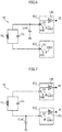
- FIG. 6 and 7 provide further details of possible embodiments along the lines of Figures 2-3 and 4-5 , wherein the I/O PADs of e.g. a microcontroller such as D in Figure 1 may include internal switches S1, S2 (possibly admitting connection to a source Vdd, to ground GND and "open", e.g. floating) as well as Schmitt triggers 141, 142.
- the I/O PADs of e.g. a microcontroller such as D in Figure 1 may include internal switches S1, S2 (possibly admitting connection to a source Vdd, to ground GND and "open", e.g. floating) as well as Schmitt triggers 141, 142.
- circuit diagrams of Figures 6 and 7 are exemplary of arrangements providing good power efficiency by resorting to "clock-less" operation where the excitation time may be controlled by the PAD's via Schmitt triggers and the capacitors Cs and C ref , thus dispensing with high frequency clock sources, with the measurement process adapted to be driven e.g. by a low speed RTC clock (e.g. LSE) that has the basic task of triggering new measurements.
- a low speed RTC clock e.g. LSE
- circuit diagrams of Figures 6 and 7 are exemplary of two implementation schemes:
- a direct charge mechanism may permit to use a smaller C ref with respect to a charge-sharing scheme.
- the senor 10 will be charged by means of a controlled transfer of charge from C ref .
- C ref may be selected with a capacity large enough to store an adequate amount of charge for exciting the sensor 10 and to hold a residual energy in the capacitor (Vmid voltage).
- One or more embodiments as exemplified in Figure 6 may involve two different charge steps: in the former C ref is fully loaded at Vdd and in the latter the accumulated energy is transferred to the sensor 10.
- operation of an arrangement as exemplified in Figure 6 may involve the following steps performed to complete a measurement stage:
- a single sensor 10 may be set between two PADs 101 and 102: in one or more embodiments, that configuration may be extended to cover multiple sensors 10 both in 4 PAD or 6 PAD configurations).
- the PAD 101 may have two main tasks:
- the PAD 102 may have the following main tasks:
- operation of an arrangement as exemplified in Figure 7 may involve the following steps performed to complete a measurement stage:
- the final part of the smooth oscillation may cross the trigger threshold (Vth) with a reduced slope, which may expose the device at the noise: some extra pulse can be generated if a noise with a sufficient amplitude occurs near the Vth crossing.
- noise immunity may be pursued by reducing the time over which the smooth oscillation is near the Vth threshold.
- that result may be achieved by moving the detection phase near the first phase of the oscillation where the slope of the waveform is sharpest and/or by moving dynamically the Vmid voltage during the measurement time.
- the first solution may be applied by reducing the Vmid voltage value.
- a clock-less charge-sharing solution as exemplified in Figure 6 one may activate the PD on the PAD 102 to decrease the Vmid voltage during the oscillation.
- a register may be used to select how many pulses are counted before the PD is enabled, and a register may be similarly used to enable the dynamic PD feature.
- the I02/ZI feedback can be "stretched" to reduce the Vmid voltage with a programmable delay (e.g. a register).
Description
- The description relates to inductive (LC) sensors.
- One or more embodiments may apply to LC sensors for use, e.g. in fluid metering applications, such as water and gas meters.
- Inductive sensing is based on an inductor-capacitor resonant circuit (which explains the current designation of "LC sensing") which is pumped by an oscillator with the inductor acting as a sensing coil. As a conductive (e.g. metal) object comes in the vicinity of the coil, currents are generated in the object depending on various parameters such as e.g. the material and dimensions of the object and/or the distance to the sensing coil. The currents thus generated form a magnetic field which reduces the oscillation amplitude of the resonant circuit (tank) thus changing the parallel resonance impedance of the circuit. Detecting/measuring such change may be exploited for various sensing purposes.
- Inductive/LC sensing may be used in various industrial fields for e.g. various types of contactless sensing of moving parts for various purposes such as detecting/measuring distance, speed or flow.
- For instance, inductive/LC sensing is being increasingly applied e.g. in water and gas meter applications with the possibility of offering power/efficient solution adapted to be directly embedded e.g.in MicroController Units - MCUs.
- In such a possible context of use, factors such as e.g. reducing the number of (analog) components coupled with the sensor, facilitating digital processing of the sensing signals and simplifying control logic while providing reduced consumption may play a significant role.
- Reducing the time involved in performing a certain measurement and/or the capability of handling multiple sensors represent a further factors of interest.
- Time-based LC sensor excitation using e.g. a high-speed (e.g. 4MHz) clock source to control transfer of energy during excitation has been used with potential drawbacks represented e.g. by power consumption and total measurement times in the range of e.g. 50 microseconds.
- The need is therefore felt for improved arrangements which may dispense with these and other drawbacks. More specifically, the present invention relates to a method of operating LC sensors according to the preamble of claim 1, which is known, e.g. from
US 4618835 A . Also, documentsGB 2204135 A US 2008/204206 A1 are of interest for the invention. - An object of one or more embodiments is to provide a response to such a need.
- According to one or more embodiments, such an object may be achieved thanks to a method having the features set forth in claim 1 that follows.
- One or more embodiments may also relate to a corresponding device according to claim 4 as well as to apparatus (e.g. metering device such as a water or gas meter) according to claim 8 including such a device.
- The claims are an integral part of the disclosure of one or more embodiments as provided herein.
- One or more embodiments may offer one or more of the following advantages:
- reduce the power absorption (no high-speed clock needed)
- insensitivity to Power Voltage-Temperature - PVT factors, (due to the possibility of resorting to closed-loop control),
- robustness against PVT variations also in the field, that is in current operation.
- One or more embodiments will now be described, by way of example only, with reference to the annexed figures, wherein:
-
Figure 1 is a generally representative of a possible context of use of one or more embodiments; -
Figure 2 is a block diagram exemplary of embodiments; -
Figure 3 is a another block diagram exemplary of embodiments; -
Figure 4 is a further block diagram exemplary of embodiments; -
Figure 5 is a another further block diagram exemplary of embodiments; and -
Figures 6 and 7 are schematic diagrams exemplary of circuit layouts according to one or more embodiments. - In the ensuing description, one or more specific details are illustrated, aimed at providing an in-depth understanding of examples of embodiments. The embodiments may be obtained without one or more of the specific details, or with other methods, components, materials, etc. In other cases, known structures, materials, or operations are not illustrated or described in detail so that certain aspects of embodiments will not be obscured.
- Reference to "an embodiment" or "one embodiment" in the framework of the present description is intended to indicate that a particular configuration, structure, or characteristic described in relation to the embodiment is comprised in at least one embodiment. Hence, phrases such as "in an embodiment" or "in one embodiment" that may be present in one or more points of the present description do not necessarily refer to one and the same embodiment. Moreover, particular conformations, structures, or characteristics may be combined in any adequate way in one or more embodiments.
- The references used herein are provided merely for convenience and hence do not define the extent of protection or the scope of the embodiments.
- The schematic diagram of
Figure 1 is generally exemplary of possible applications of inductive/LC sensing: these designations will be hereinafter used as synonyms having regard to the general principle of operation of such sensors as summarized in the introduction of this description. - The schematic diagram of
Figure 1 is exemplary of a possible application of inductive/LC sensors 10 in a fluid metering device such as a flow-meter (e.g. water or gas meter) in order to detect/measure fluid flow in a conduit C. This may take place, in manner known per se, by detecting/measuring movement of a rotary sensing plate P which is driven in rotation by fluid flow in the conduit C. - For instance, the rotary plate P may include complementary portions of different materials (e.g. conductive and non-conductive). One or
more LC sensors 10 arranged facing the plate P may thus produce signals indicative of rotation of the plate P (and thus of the flow in the conduit C) for processing in e.g. a MicroController Unit - MCU. - The general principles underlying the structure and operation of such metering device are otherwise known in the art, which makes it unnecessary to provide a more detailed description herein. Also, it will be appreciated that the application exemplified in
Figure 1 is just one of a wide variety of possible applications of inductive/LC sensor 10, one or more embodiments being otherwise primarily concerned with managing operation of such an LC sensor. - In one or more embodiments, operation of an
LC sensor 10 as exemplified herein may generally involve at least one charging phase wherein excitation energy for thesensor 10 is accumulated. The LC sensor (here exemplified as the parallel connection of an inductor Ls and a capacitor Cs) may thus oscillate energized by the energy accumulated to permit sensing to take place as outlined in the introduction to this description. - In conventional solutions, energy accumulation (charging) may be stopped at a certain time as defined e.g. by a high-frequency (e.g. 4MHz clock source).
- By way of contrast, one or more embodiments as exemplified herein may provide for detecting (e.g. by a charge sensor/energy meter 12) the fact that the energy accumulated has reached a certain charge accumulation threshold, with operation switched towards the sensing phase when the charge threshold is detected to be reached.
- In one or more embodiments as exemplified in
Figure 2 the excitation energy from an electric energy source V (of any known type for that purpose) may be accumulated by charging a reference capacitor Cref. - One or more embodiments as exemplified in
Figure 2 may include a first switch S1 ad a second switch S2 (e.g. electronic switches such as MOSFETs) switchable under the control of anenergy meter 12 configured for sensing the charge on the reference capacitor Cref (e.g. the voltage across the reference capacitor Cref). - When the switch S1 is closed, that is conductive, the reference capacitor Cref is set between the source V and ground, and the
sensor 10 may be set between the source V and the switch S2, with the switch S2 set between thesensor 10 and ground. - In one or more embodiments, operation of the circuit layout exemplified in
Figure 2 may include: - pre-charge of Cref: S2 is open - that is non-conductive - so that the
sensor 10 is "floating" with respect to ground, and S1 is closed - that is conductive - until the voltage on Cref reaches a value VCref_INIT (<= V) with S1 subsequently open - that is non conductive; - energy transfer: S1 is open and S2 closed, so that the energy accumulated on Cref is (partially) transferred onto the sensor 10 (which is essentially in parallel to Cref) . Controlled transfer of energy terminates when the voltage across Cref reaches a final target value VCref_FIN, after which the switch S2 is opened. In that way, the amount of energy transferred is (ideally) equal to 0.5 Cref (VCref_INIT - VCref_FIN)2;
- measurement: both S1 and S2 are open. The sensor will start oscillating around the voltage value VCref_FIN, with such oscillation adapted to be monitored via the pin towards the switch S2.
- The circuit may then be reset and the sequence exemplified in the foregoing repeated for a new measurement.
-
Figure 3 is exemplary of the possibility of implementing a similar mode of operation in an arrangement where the inner resistance R of the source (generator) V may play the role of the switch S1, by assuming that the time constant T = R∗Cref is much higher than the time needed for performing the measurement, which is reasonably the case if e.g. the internal pull-up of the address data bus or PAD of microcontroller D is used as the voltage generator V. - In one or more embodiments, operation of the circuit layout exemplified in
Figure 3 may again include: - pre-charge of Cref: S2 is open and the
energy meter 12 monitors that Cref is charged to an energy accumulation threshold voltage e.g. V; - energy transfer: S2 is closed and the energy accumulated on Cref is partially transferred onto the sensore10. Controlled transfer of energy terminates when the voltage across Cref reaches a final target value VCREF_FIN, after which the switch S2 is opened. In that way, the amount of energy transferred is (ideally) equal to 0.5 CreF (V- VCref_FIN)2. The energy from the generator may be neglected due to the high value of the time constant.
- measurement: S2 is open. The sensor will start oscillating around the voltage value VCref_FIN, with such oscillation adapted to be monitored via the pin towards the switch S2. The voltage variation on Cref due to recharging via the generator V may again be neglected due to the time constant T = R∗Cref being much higher than the time needed for performing the measurement.
- In one or more embodiments as exemplified in
Figure 4 a reference capacitor Cref may again be used, by coupling it in series with theLC sensor 10, with the series connection of thesensor 10 and the reference capacitor Cref set between a switch S1 (again an electronic switch such as a MOSFET: the same designation ofFigure 2 is used for simplicity) and ground with the reference capacitor Cref between thesensor 10 and ground. - In one or more embodiments as exemplified in
Figure 4 , anenergy sensing meter 12 may again be provided capable of sensing the charge on the reference capacitor Cref (e.g. the voltage across the reference capacitor Cref) and driving the switch S1 which is arranged between the source V and thesensor 10. - In one or more embodiments as exemplified in
Figure 4 , the switch S1 between the source V and thesensor 10 may be closed (that is, conductive) while energy is being accumulated on the reference capacitor Cref via thesensor 10. When a certain charge threshold is detected to be reached (as dictated by the characteristics and intended mode of operation of the sensor) on the reference capacitor Cref theenergy meter 12 may open the switch S1. - In one or more embodiments, operation as described above may involve both excitation of the
sensor 10 and charging the capacitor Cref (that is thesensor 10 is excited by the current flowing through Cref). - Such a charging/excitation process terminates when the charge, that is the voltage on Cref reaches a target threshold value.
- By way of reference to the exemplary layouts of
Figures 2 and 3 , the arrangement exemplified inFigure 4 may be regarded as somewhat joining pre-charge and energy transfer (charge sharing) with excitation of the sensor and generation of the voltage Cref about which oscillation will occur taking place in a single step. - In one or more embodiments as exemplified in
Figure 4 measurement may involve opening the switch S1, with thesensor 10 starting oscillating about the value of the voltage charged onto Cref, and the pin towards S1 (which remains floating since S1 is open) adapted to be used for monitoring the (damped) oscillation, with Cref primarily providing a reference for the voltage about which sensor oscillation will take place - The circuit may then be reset and the sequence exemplified in the foregoing repeated for a new measurement.
-
Figure 5 is exemplary of the possibility of implementing a similar mode of operation by making sensor excitation independent of generation of the oscillation voltage on Cref. - In comparison with the exemplary circuit layout of
Figure 4 , the exemplary circuit layout ofFigure 5 involves: - a second switch S2 (again an electronic switch such as a MOSFET: the same designation of
Figures 2 and 3 is used for simplicity) set between thesensor 10 and ground, that is in parallel to the capacitor Cref; - the
energy meter 12 configured for driving the switches S1 and S2 as a function of the voltage at a point between the switch S1 and thesensor 10. - In one or more embodiments, operation of the circuit layout exemplified in
Figure 5 may include: - excitation: S1, S2 both closed, with the
sensor 10 set between the voltage V and ground. Theenergy meter 12 is sensitive to the amount of energy transferred; Cref kept uncharged as it is grounded on both sides; - post excitation and generation of Vref: S1 closed and S2 open. Charging of the
sensor 10 is completed and the capacitor Cref is charged to a final value VCre FIN; - measurement: S1 and S2 both open, with the sensor oscillation about the voltage VCref_FIN, and oscillation adapted to be monitored on the "floating" pin of the switch S1 opposed to the source V.
- Various other implementations are feasible in one or more embodiments.
- Just to mention one possibility, in one or more embodiments, the switch S2 may connect directly Cref to the generator V, so that VCref_FIN may be generated directly instead of via the
sensor 10. - The circuit diagrams of
Figures 6 and 7 provide further details of possible embodiments along the lines ofFigures 2-3 and4-5 , wherein the I/O PADs of e.g. a microcontroller such as D inFigure 1 may include internal switches S1, S2 (possibly admitting connection to a source Vdd, to ground GND and "open", e.g. floating) as well as Schmitt triggers 141, 142. - In
Figures 6 and 7 the same reference symbols are used to denote parts of elements already introduced in connection withFigures 2 to 5 without repeating the related description for the sake of brevity. - The circuit diagrams of
Figures 6 and 7 are exemplary of arrangements providing good power efficiency by resorting to "clock-less" operation where the excitation time may be controlled by the PAD's via Schmitt triggers and the capacitors Cs and Cref, thus dispensing with high frequency clock sources, with the measurement process adapted to be driven e.g. by a low speed RTC clock (e.g. LSE) that has the basic task of triggering new measurements. - The circuit diagrams of
Figures 6 and 7 are exemplary of two implementation schemes: - a clock-less charge sharing scheme, including a pre-charge step where a reference capacitor Cref is preloaded by a
PAD 101 with a maximum voltage (Vdd) and a second step where the accumulated energy is transferred to thesensor 10 to excite and generate the reference voltage on Cref (Figure 6 ); and - a clock-less direct charge scheme, where excitation of the
sensor 10 and generation of the reference voltage are driven by two PADs, e.g. 101, 102, with two charge steps, e.g. pre-charge and post-charge (Figure 7 ). - A direct charge mechanism may permit to use a smaller Cref with respect to a charge-sharing scheme.
- In one or more embodiments as exemplified in
Figure 6 , thesensor 10 will be charged by means of a controlled transfer of charge from Cref. In this case Cref may be selected with a capacity large enough to store an adequate amount of charge for exciting thesensor 10 and to hold a residual energy in the capacitor (Vmid voltage). - One or more embodiments as exemplified in
Figure 6 may involve two different charge steps: in the former Cref is fully loaded at Vdd and in the latter the accumulated energy is transferred to thesensor 10. - In one or more embodiments, operation of an arrangement as exemplified in
Figure 6 may involve the following steps performed to complete a measurement stage: - reset and pre-charge: both switches S1 and S2 are closed to Vdd, the
sensor 10 will be discharged while Cref is precharged to Vdd. The residual energy in the capacitor (Vmid voltage) is held and used as starting point for this step; - charge sharing: the switch S1 is open while the switch S2 is closed to GND. With this configuration Cref provides the energy required to load the
sensor 10. This step will be completed when the trigger 101 (ZI input) reaches a logic "0" (with the 101 voltage at VthL). The amount of transferred energy is 0.5 Cref (Vdd -Vthl)2; - sensor oscillation: both switches S1 and S2 are open and the oscillation may be monitored via the 102/ZI pin.
- In fact, the voltage Vmid = VthL about which oscillation takes place may be present on 101 while VI02 = Vsensor + V101 => V102 = (Vsensor + VthL)/ZI pin.
- In the arrangement exemplified in
Figure 7 , asingle sensor 10 may be set between twoPADs 101 and 102: in one or more embodiments, that configuration may be extended to covermultiple sensors 10 both in 4 PAD or 6 PAD configurations). - In one or more embodiments as exemplified in
Figure 7 , thePAD 101 may have two main tasks: - providing the current to charge/reset the
sensor 10 and Cref; - triggering the start of the post-charge phase (101 Schmitt trigger 141).
- In one or more embodiments as exemplified in
Figure 7 , thePAD 102 may have the following main tasks: - discharging the
sensor 10 during a reset state; - triggering the end of a post-charge phase looking at its voltage level (Schmitt trigger 142);
- tuning and controlling the voltage on Cref during the oscillation time.
- In one or more embodiments, operation of an arrangement as exemplified in
Figure 7 may involve the following steps performed to complete a measurement stage: - reset: switch S1 and switch S2 are closed to GND, both the
sensor 10 and the capacitance Cref are shorted to GND; - pre-charge: the switch S1 is closed to Vdd while the switch S2 is closed to GND. In this initial phase the inductor Ls can be assumed to be an open circuit for an
exemplary sensor 10, with the capacitor Cs set between Vdd and GND and Cref connected to GND, so that the sensor capacitor Cs will be charged ; the pre-charge duration will be completed when the 101 trigger (ZI input) reaches e.g. a "1" logic level, with Cs pre-charged to a value VthH so that the energy transferred to thesensor 10 is 0.5 Cs VthH2; - post-charge: the switch S1 is closed to Vdd while the switch S2 is open (high impedance). In this step sensor excitation will be completed and the reference voltage on Cref generated. The post-charge will be completed when the 102 trigger (ZI input) will reach a "1" logic level. At the end of this step Cref will be pre-charged to VthH and the sensor fully charged. For high values of Cref the sensor inductor current may not be negligible, and the
PAD 101 will provide both the energy for the inductor Ls plus the energy for Cref; - Vref range stabilization and oscillation measure: when the 102 voltage reaches VthH, the switch S1 will be open (end of post-charge step) while the switch S2 will be configured to keep the 102 voltage below VthH: the PAD will drive a logic "0" (PullDown or PushPull depending of register configuration) any time that the I02/ZI is one. The 102 configuration ensures that the Cref voltage is kept below the VthH voltage value: for instance, for 5 Volt- tolerant PADs there are some parasitic effects (diode) that may increase the Vref voltage during oscillation of the
sensors 10 in case this goes below GND. The dumped oscillation will be observed by the I01/ZI pin. - In one or more embodiments exemplifies herein, the final part of the smooth oscillation may cross the trigger threshold (Vth) with a reduced slope, which may expose the device at the noise: some extra pulse can be generated if a noise with a sufficient amplitude occurs near the Vth crossing. In one or more embodiments, noise immunity may be pursued by reducing the time over which the smooth oscillation is near the Vth threshold. In one or more embodiments that result may be achieved by moving the detection phase near the first phase of the oscillation where the slope of the waveform is sharpest and/or by moving dynamically the Vmid voltage during the measurement time.
- The first solution may be applied by reducing the Vmid voltage value. For a clock-less charge-sharing solution as exemplified in
Figure 6 one may activate the PD on thePAD 102 to decrease the Vmid voltage during the oscillation. A register may be used to select how many pulses are counted before the PD is enabled, and a register may be similarly used to enable the dynamic PD feature. For a clock-less solution as exemplified inFigure 7 , during the Vref range stabilization step the I02/ZI feedback can be "stretched" to reduce the Vmid voltage with a programmable delay (e.g. a register). - Without prejudice to the underlying principles, the details and embodiments may vary, even significantly, with respect to what has been described by way of example only, without departing from the extent of protection.
- The extent of protection is determined by the claims that follow.
Claims (8)
- A method of operating LC sensors (10) including:- accumulating excitation energy for an LC sensor (10), and- the LC sensor (10) oscillating energized by energy accumulated,wherein the method includes:- detecting (12) the energy accumulated reaching a charge threshold, and- terminating accumulating excitation energy for the sensor (10) when the charge threshold is detected (12) to be reached,
the method characterized in that it includes coupling a reference capacitor (Cref) in series to the LC sensor (10), and- a) accumulating excitation energy for the sensor (10) by coupling (S1) the series coupling of the sensor (10) and the reference capacitor (Cref) to an energy source (V), or- b) starting accumulating excitation energy for the sensor (10) by coupling (S1) the sensor (10) to an energy source (V) with the reference capacitor (Cref) short-circuited (S2), and removing the short-circuit across the reference capacitor (Cref) while maintaining the LC sensor (10) coupled to the energy source (V). - The method of claim 1, including detecting (12) the energy accumulated reaching a charge threshold by detecting the voltage across the reference capacitor (Cref) reaching a voltage threshold.
- The method of claim 1 or claim 2, including a reset step wherein a zero-voltage drop is applied (S1, S2) across the LC sensor (10).
- An LC sensor device, including:- energy accumulation means for accumulating excitation energy,- an LC sensor (10) configured for oscillating energized by energy accumulated,wherein the device includes:- an energy detector (12) for detecting the energy accumulated in the energy accumulation means reaching a charge threshold, and- at least one switch (S1, S2) coupled with the energy detector (12) for terminating accumulating excitation energy for the sensor (10) on the energy accumulation means when the charge threshold is detected to be reached by the energy detector (12),the device characterized in that it includes:- a reference capacitor (Cref) in series to the LC sensor (10) for accumulating excitation energy for the sensor (10), and- an energy source (V), wherein- a) the series coupling of the sensor (10) and the reference capacitor (Cref) Z coupled to the energy source (V), or- b) the at least one switch comprises a first and a second switch, wherein the first switch (S1) couples (S1) the sensor (10) to the energy source (Vdd) with the reference capacitor (Cref) short-circuited by the second switch (S2), the second switch (S2) switchable for removing the short-circuit across the reference capacitor (Cref) with the LC sensor (10) coupled to the energy source (Vdd) by the first switch (S1).
- The LC sensor device of claim 4, wherein the energy detector (12) is configured for detecting the energy accumulated reaching a charge threshold by detecting the voltage across the reference capacitor (Cref) reaching a voltage threshold.
- The LC sensor device of any of claim 4 or claim 5, including switch means (S1, S2) for selectively applying a zero-voltage drop across the LC sensor (10).
- The LC sensor device of any of claims 4 to 6, including a controller unit (D) providing at least one of:- the at least one switch (S1, S2) coupled with the energy detector (12) for terminating accumulating excitation energy for the sensor (10) on the energy accumulation means when the charge threshold is detected to be reached by the energy detector (12), and /or- sensing means (141, 142) for sensing oscillation of the LC sensor (10) oscillating energized by energy accumulated.
- Apparatus, preferably a fluid flow sensing device, including a device according to any of claims 4 to 7.
Applications Claiming Priority (1)
| Application Number | Priority Date | Filing Date | Title |
|---|---|---|---|
| ITUB2015A003537A ITUB20153537A1 (en) | 2015-09-10 | 2015-09-10 | OPERATION PROCEDURE OF LC SENSORS, SYSTEM AND CORRESPONDING EQUIPMENT |
Publications (2)
| Publication Number | Publication Date |
|---|---|
| EP3141871A1 EP3141871A1 (en) | 2017-03-15 |
| EP3141871B1 true EP3141871B1 (en) | 2020-04-29 |
Family
ID=54601960
Family Applications (1)
| Application Number | Title | Priority Date | Filing Date |
|---|---|---|---|
| EP16162411.9A Active EP3141871B1 (en) | 2015-09-10 | 2016-03-24 | A method of operating lc sensors, corresponding system and apparatus |
Country Status (3)
| Country | Link |
|---|---|
| US (2) | US10120006B2 (en) |
| EP (1) | EP3141871B1 (en) |
| IT (1) | ITUB20153537A1 (en) |
Families Citing this family (2)
| Publication number | Priority date | Publication date | Assignee | Title |
|---|---|---|---|---|
| ES2956816T3 (en) * | 2018-11-22 | 2023-12-28 | Behr Hella Thermocontrol Gmbh | Procedure and device for controlling a tensile armature magnet |
| DE102020100939A1 (en) * | 2020-01-16 | 2021-07-22 | Turck Holding Gmbh | Proximity switch and method for detecting an object to be detected |
Family Cites Families (13)
| Publication number | Priority date | Publication date | Assignee | Title |
|---|---|---|---|---|
| US4001718A (en) * | 1975-05-12 | 1977-01-04 | Electro Corporation | Linear oscillator for proximity sensor |
| US4618835A (en) * | 1984-11-27 | 1986-10-21 | Maranantha Research Ltd. | Proximity sensor oscillator utilizing controlled charge |
| US4851770A (en) * | 1985-02-11 | 1989-07-25 | Sensor Technologies, Inc. | Displacement sensor having dual tank circuits |
| FR2614432B1 (en) * | 1987-04-23 | 1989-07-28 | Telemecanique Electrique | INDUCTIVE PROXIMITY DETECTOR |
| DE4325406B4 (en) * | 1992-09-02 | 2006-02-23 | Tiefenbach Gmbh | proximity switch |
| US5576628A (en) * | 1994-09-30 | 1996-11-19 | Telcom Semiconductor, Inc. | Method and apparatus to measure capacitance |
| DE10130572B4 (en) * | 2001-06-27 | 2010-01-07 | Ifm Electronic Gmbh | Inductive displacement sensor for determining the position of an influencing element and method for determining the position of an influencing element with an inductive displacement sensor |
| US6646454B2 (en) * | 2002-01-07 | 2003-11-11 | Test-Um, Inc. | Electronic apparatus and method for measuring length of a communication cable |
| US7528597B2 (en) * | 2004-03-08 | 2009-05-05 | Digisensors, Inc. | Induction sensor |
| ES2297359T3 (en) * | 2004-03-26 | 2008-05-01 | Senstronic, S.A. | INDUCTIVE PROXIMITY SENSOR. |
| DE102004039401A1 (en) * | 2004-08-13 | 2006-03-09 | Siemens Ag | Transceiver transponder system |
| US7511476B2 (en) * | 2005-01-04 | 2009-03-31 | Digisensors, Inc. | Electromagnetic sensor systems and methods of use thereof |
| DE102007003374A1 (en) * | 2006-02-22 | 2007-09-20 | Pepperl + Fuchs Gmbh | Inductive proximity switch and method for operating such |
-
2015
- 2015-09-10 IT ITUB2015A003537A patent/ITUB20153537A1/en unknown
-
2016
- 2016-03-15 US US15/070,509 patent/US10120006B2/en active Active
- 2016-03-24 EP EP16162411.9A patent/EP3141871B1/en active Active
-
2018
- 2018-09-19 US US16/136,121 patent/US10859617B2/en active Active
Non-Patent Citations (1)
| Title |
|---|
| None * |
Also Published As
| Publication number | Publication date |
|---|---|
| ITUB20153537A1 (en) | 2017-03-10 |
| US10859617B2 (en) | 2020-12-08 |
| US20170074914A1 (en) | 2017-03-16 |
| EP3141871A1 (en) | 2017-03-15 |
| US10120006B2 (en) | 2018-11-06 |
| US20190018051A1 (en) | 2019-01-17 |
Similar Documents
| Publication | Publication Date | Title |
|---|---|---|
| US7586303B2 (en) | Inductive proximity sensor | |
| CN100392356C (en) | Position sensor | |
| US20130093436A1 (en) | Electromagnetic method for sensing the relative position of two items using coupled tuned circuits | |
| US10852451B2 (en) | System for interfacing an LC sensor, related method and computer program product | |
| US10859617B2 (en) | Method of operating LC sensors, corresponding system and apparatus | |
| JP6228543B2 (en) | Differential current measurement to determine ionic current in the presence of leakage current | |
| CN107229277A (en) | A kind of steep cliff detection circuit and its sweeping robot | |
| US9038480B2 (en) | Integrated circuit and apparatus for detecting oscillations | |
| CN105319599B (en) | Dock the method and its system of LC sensors | |
| US10756732B2 (en) | Inductive sensor and method for operating an inductive sensor | |
| US11588353B2 (en) | Quality factor estimation of an inductive element | |
| JP4409765B2 (en) | Micro power magnetometer | |
| US20080084203A1 (en) | Pulsed coil drive circuit for a sampled inductive transducer | |
| JP2002527718A5 (en) | ||
| KR100370484B1 (en) | Device for detecting metallic body | |
| JP2003329404A (en) | Position detector in hydraulic flow rate control valve | |
| JP2003156304A (en) | Position detector in fluid pressure cylinder | |
| JP2000321248A (en) | Oil check sensor | |
| JP2003328846A (en) | Fuel injection amount detector in overflow type fuel injection pump device for diesel engine | |
| JPH08159741A (en) | Displacement detection device |
Legal Events
| Date | Code | Title | Description |
|---|---|---|---|
| PUAI | Public reference made under article 153(3) epc to a published international application that has entered the european phase |
Free format text: ORIGINAL CODE: 0009012 |
|
| STAA | Information on the status of an ep patent application or granted ep patent |
Free format text: STATUS: THE APPLICATION HAS BEEN PUBLISHED |
|
| AK | Designated contracting states |
Kind code of ref document: A1 Designated state(s): AL AT BE BG CH CY CZ DE DK EE ES FI FR GB GR HR HU IE IS IT LI LT LU LV MC MK MT NL NO PL PT RO RS SE SI SK SM TR |
|
| AX | Request for extension of the european patent |
Extension state: BA ME |
|
| STAA | Information on the status of an ep patent application or granted ep patent |
Free format text: STATUS: REQUEST FOR EXAMINATION WAS MADE |
|
| 17P | Request for examination filed |
Effective date: 20170906 |
|
| RBV | Designated contracting states (corrected) |
Designated state(s): AL AT BE BG CH CY CZ DE DK EE ES FI FR GB GR HR HU IE IS IT LI LT LU LV MC MK MT NL NO PL PT RO RS SE SI SK SM TR |
|
| GRAP | Despatch of communication of intention to grant a patent |
Free format text: ORIGINAL CODE: EPIDOSNIGR1 |
|
| STAA | Information on the status of an ep patent application or granted ep patent |
Free format text: STATUS: GRANT OF PATENT IS INTENDED |
|
| INTG | Intention to grant announced |
Effective date: 20191120 |
|
| GRAS | Grant fee paid |
Free format text: ORIGINAL CODE: EPIDOSNIGR3 |
|
| GRAA | (expected) grant |
Free format text: ORIGINAL CODE: 0009210 |
|
| STAA | Information on the status of an ep patent application or granted ep patent |
Free format text: STATUS: THE PATENT HAS BEEN GRANTED |
|
| AK | Designated contracting states |
Kind code of ref document: B1 Designated state(s): AL AT BE BG CH CY CZ DE DK EE ES FI FR GB GR HR HU IE IS IT LI LT LU LV MC MK MT NL NO PL PT RO RS SE SI SK SM TR |
|
| REG | Reference to a national code |
Ref country code: GB Ref legal event code: FG4D |
|
| REG | Reference to a national code |
Ref country code: CH Ref legal event code: EP |
|
| REG | Reference to a national code |
Ref country code: DE Ref legal event code: R096 Ref document number: 602016034904 Country of ref document: DE |
|
| REG | Reference to a national code |
Ref country code: AT Ref legal event code: REF Ref document number: 1263990 Country of ref document: AT Kind code of ref document: T Effective date: 20200515 |
|
| REG | Reference to a national code |
Ref country code: IE Ref legal event code: FG4D |
|
| REG | Reference to a national code |
Ref country code: NL Ref legal event code: MP Effective date: 20200429 |
|
| REG | Reference to a national code |
Ref country code: LT Ref legal event code: MG4D |
|
| PG25 | Lapsed in a contracting state [announced via postgrant information from national office to epo] |
Ref country code: GR Free format text: LAPSE BECAUSE OF FAILURE TO SUBMIT A TRANSLATION OF THE DESCRIPTION OR TO PAY THE FEE WITHIN THE PRESCRIBED TIME-LIMIT Effective date: 20200730 Ref country code: LT Free format text: LAPSE BECAUSE OF FAILURE TO SUBMIT A TRANSLATION OF THE DESCRIPTION OR TO PAY THE FEE WITHIN THE PRESCRIBED TIME-LIMIT Effective date: 20200429 Ref country code: NO Free format text: LAPSE BECAUSE OF FAILURE TO SUBMIT A TRANSLATION OF THE DESCRIPTION OR TO PAY THE FEE WITHIN THE PRESCRIBED TIME-LIMIT Effective date: 20200729 Ref country code: IS Free format text: LAPSE BECAUSE OF FAILURE TO SUBMIT A TRANSLATION OF THE DESCRIPTION OR TO PAY THE FEE WITHIN THE PRESCRIBED TIME-LIMIT Effective date: 20200829 Ref country code: SE Free format text: LAPSE BECAUSE OF FAILURE TO SUBMIT A TRANSLATION OF THE DESCRIPTION OR TO PAY THE FEE WITHIN THE PRESCRIBED TIME-LIMIT Effective date: 20200429 Ref country code: PT Free format text: LAPSE BECAUSE OF FAILURE TO SUBMIT A TRANSLATION OF THE DESCRIPTION OR TO PAY THE FEE WITHIN THE PRESCRIBED TIME-LIMIT Effective date: 20200831 Ref country code: FI Free format text: LAPSE BECAUSE OF FAILURE TO SUBMIT A TRANSLATION OF THE DESCRIPTION OR TO PAY THE FEE WITHIN THE PRESCRIBED TIME-LIMIT Effective date: 20200429 |
|
| REG | Reference to a national code |
Ref country code: AT Ref legal event code: MK05 Ref document number: 1263990 Country of ref document: AT Kind code of ref document: T Effective date: 20200429 |
|
| PG25 | Lapsed in a contracting state [announced via postgrant information from national office to epo] |
Ref country code: RS Free format text: LAPSE BECAUSE OF FAILURE TO SUBMIT A TRANSLATION OF THE DESCRIPTION OR TO PAY THE FEE WITHIN THE PRESCRIBED TIME-LIMIT Effective date: 20200429 Ref country code: HR Free format text: LAPSE BECAUSE OF FAILURE TO SUBMIT A TRANSLATION OF THE DESCRIPTION OR TO PAY THE FEE WITHIN THE PRESCRIBED TIME-LIMIT Effective date: 20200429 Ref country code: BG Free format text: LAPSE BECAUSE OF FAILURE TO SUBMIT A TRANSLATION OF THE DESCRIPTION OR TO PAY THE FEE WITHIN THE PRESCRIBED TIME-LIMIT Effective date: 20200729 Ref country code: LV Free format text: LAPSE BECAUSE OF FAILURE TO SUBMIT A TRANSLATION OF THE DESCRIPTION OR TO PAY THE FEE WITHIN THE PRESCRIBED TIME-LIMIT Effective date: 20200429 |
|
| PG25 | Lapsed in a contracting state [announced via postgrant information from national office to epo] |
Ref country code: AL Free format text: LAPSE BECAUSE OF FAILURE TO SUBMIT A TRANSLATION OF THE DESCRIPTION OR TO PAY THE FEE WITHIN THE PRESCRIBED TIME-LIMIT Effective date: 20200429 Ref country code: NL Free format text: LAPSE BECAUSE OF FAILURE TO SUBMIT A TRANSLATION OF THE DESCRIPTION OR TO PAY THE FEE WITHIN THE PRESCRIBED TIME-LIMIT Effective date: 20200429 |
|
| PG25 | Lapsed in a contracting state [announced via postgrant information from national office to epo] |
Ref country code: SM Free format text: LAPSE BECAUSE OF FAILURE TO SUBMIT A TRANSLATION OF THE DESCRIPTION OR TO PAY THE FEE WITHIN THE PRESCRIBED TIME-LIMIT Effective date: 20200429 Ref country code: EE Free format text: LAPSE BECAUSE OF FAILURE TO SUBMIT A TRANSLATION OF THE DESCRIPTION OR TO PAY THE FEE WITHIN THE PRESCRIBED TIME-LIMIT Effective date: 20200429 Ref country code: RO Free format text: LAPSE BECAUSE OF FAILURE TO SUBMIT A TRANSLATION OF THE DESCRIPTION OR TO PAY THE FEE WITHIN THE PRESCRIBED TIME-LIMIT Effective date: 20200429 Ref country code: CZ Free format text: LAPSE BECAUSE OF FAILURE TO SUBMIT A TRANSLATION OF THE DESCRIPTION OR TO PAY THE FEE WITHIN THE PRESCRIBED TIME-LIMIT Effective date: 20200429 Ref country code: ES Free format text: LAPSE BECAUSE OF FAILURE TO SUBMIT A TRANSLATION OF THE DESCRIPTION OR TO PAY THE FEE WITHIN THE PRESCRIBED TIME-LIMIT Effective date: 20200429 Ref country code: AT Free format text: LAPSE BECAUSE OF FAILURE TO SUBMIT A TRANSLATION OF THE DESCRIPTION OR TO PAY THE FEE WITHIN THE PRESCRIBED TIME-LIMIT Effective date: 20200429 Ref country code: IT Free format text: LAPSE BECAUSE OF FAILURE TO SUBMIT A TRANSLATION OF THE DESCRIPTION OR TO PAY THE FEE WITHIN THE PRESCRIBED TIME-LIMIT Effective date: 20200429 Ref country code: DK Free format text: LAPSE BECAUSE OF FAILURE TO SUBMIT A TRANSLATION OF THE DESCRIPTION OR TO PAY THE FEE WITHIN THE PRESCRIBED TIME-LIMIT Effective date: 20200429 |
|
| REG | Reference to a national code |
Ref country code: DE Ref legal event code: R097 Ref document number: 602016034904 Country of ref document: DE |
|
| PG25 | Lapsed in a contracting state [announced via postgrant information from national office to epo] |
Ref country code: PL Free format text: LAPSE BECAUSE OF FAILURE TO SUBMIT A TRANSLATION OF THE DESCRIPTION OR TO PAY THE FEE WITHIN THE PRESCRIBED TIME-LIMIT Effective date: 20200429 Ref country code: SK Free format text: LAPSE BECAUSE OF FAILURE TO SUBMIT A TRANSLATION OF THE DESCRIPTION OR TO PAY THE FEE WITHIN THE PRESCRIBED TIME-LIMIT Effective date: 20200429 |
|
| PLBE | No opposition filed within time limit |
Free format text: ORIGINAL CODE: 0009261 |
|
| STAA | Information on the status of an ep patent application or granted ep patent |
Free format text: STATUS: NO OPPOSITION FILED WITHIN TIME LIMIT |
|
| 26N | No opposition filed |
Effective date: 20210201 |
|
| PG25 | Lapsed in a contracting state [announced via postgrant information from national office to epo] |
Ref country code: SI Free format text: LAPSE BECAUSE OF FAILURE TO SUBMIT A TRANSLATION OF THE DESCRIPTION OR TO PAY THE FEE WITHIN THE PRESCRIBED TIME-LIMIT Effective date: 20200429 |
|
| PG25 | Lapsed in a contracting state [announced via postgrant information from national office to epo] |
Ref country code: MC Free format text: LAPSE BECAUSE OF FAILURE TO SUBMIT A TRANSLATION OF THE DESCRIPTION OR TO PAY THE FEE WITHIN THE PRESCRIBED TIME-LIMIT Effective date: 20200429 |
|
| REG | Reference to a national code |
Ref country code: CH Ref legal event code: PL |
|
| GBPC | Gb: european patent ceased through non-payment of renewal fee |
Effective date: 20210324 |
|
| REG | Reference to a national code |
Ref country code: BE Ref legal event code: MM Effective date: 20210331 |
|
| PG25 | Lapsed in a contracting state [announced via postgrant information from national office to epo] |
Ref country code: CH Free format text: LAPSE BECAUSE OF NON-PAYMENT OF DUE FEES Effective date: 20210331 Ref country code: LU Free format text: LAPSE BECAUSE OF NON-PAYMENT OF DUE FEES Effective date: 20210324 Ref country code: LI Free format text: LAPSE BECAUSE OF NON-PAYMENT OF DUE FEES Effective date: 20210331 Ref country code: FR Free format text: LAPSE BECAUSE OF NON-PAYMENT OF DUE FEES Effective date: 20210331 Ref country code: IE Free format text: LAPSE BECAUSE OF NON-PAYMENT OF DUE FEES Effective date: 20210324 Ref country code: GB Free format text: LAPSE BECAUSE OF NON-PAYMENT OF DUE FEES Effective date: 20210324 |
|
| PG25 | Lapsed in a contracting state [announced via postgrant information from national office to epo] |
Ref country code: BE Free format text: LAPSE BECAUSE OF NON-PAYMENT OF DUE FEES Effective date: 20210331 |
|
| PG25 | Lapsed in a contracting state [announced via postgrant information from national office to epo] |
Ref country code: HU Free format text: LAPSE BECAUSE OF FAILURE TO SUBMIT A TRANSLATION OF THE DESCRIPTION OR TO PAY THE FEE WITHIN THE PRESCRIBED TIME-LIMIT; INVALID AB INITIO Effective date: 20160324 |
|
| PGFP | Annual fee paid to national office [announced via postgrant information from national office to epo] |
Ref country code: DE Payment date: 20230221 Year of fee payment: 8 |
|
| PG25 | Lapsed in a contracting state [announced via postgrant information from national office to epo] |
Ref country code: CY Free format text: LAPSE BECAUSE OF FAILURE TO SUBMIT A TRANSLATION OF THE DESCRIPTION OR TO PAY THE FEE WITHIN THE PRESCRIBED TIME-LIMIT Effective date: 20200429 |