EP3141078B1 - Waveform differentiating repeater - Google Patents
Waveform differentiating repeater Download PDFInfo
- Publication number
- EP3141078B1 EP3141078B1 EP15714994.9A EP15714994A EP3141078B1 EP 3141078 B1 EP3141078 B1 EP 3141078B1 EP 15714994 A EP15714994 A EP 15714994A EP 3141078 B1 EP3141078 B1 EP 3141078B1
- Authority
- EP
- European Patent Office
- Prior art keywords
- signal
- block
- digital
- classification
- repeater
- Prior art date
- Legal status (The legal status is an assumption and is not a legal conclusion. Google has not performed a legal analysis and makes no representation as to the accuracy of the status listed.)
- Active
Links
- 238000004458 analytical method Methods 0.000 claims description 49
- 230000009467 reduction Effects 0.000 claims description 32
- 238000012545 processing Methods 0.000 claims description 26
- 238000000034 method Methods 0.000 claims description 14
- 238000001228 spectrum Methods 0.000 claims description 8
- 230000003068 static effect Effects 0.000 claims description 8
- 238000010183 spectrum analysis Methods 0.000 claims description 5
- 125000004122 cyclic group Chemical group 0.000 claims description 3
- 238000011084 recovery Methods 0.000 claims description 3
- 238000010586 diagram Methods 0.000 description 16
- 238000006243 chemical reaction Methods 0.000 description 11
- 238000004891 communication Methods 0.000 description 11
- 230000005540 biological transmission Effects 0.000 description 10
- 238000004549 pulsed laser deposition Methods 0.000 description 9
- 230000006870 function Effects 0.000 description 5
- 235000019800 disodium phosphate Nutrition 0.000 description 4
- 239000013598 vector Substances 0.000 description 4
- 238000007781 pre-processing Methods 0.000 description 3
- 230000006978 adaptation Effects 0.000 description 2
- 230000003321 amplification Effects 0.000 description 2
- 238000001514 detection method Methods 0.000 description 2
- 230000004069 differentiation Effects 0.000 description 2
- 230000000694 effects Effects 0.000 description 2
- 238000005516 engineering process Methods 0.000 description 2
- 238000003199 nucleic acid amplification method Methods 0.000 description 2
- 230000008569 process Effects 0.000 description 2
- 230000004044 response Effects 0.000 description 2
- 230000003595 spectral effect Effects 0.000 description 2
- 101000822695 Clostridium perfringens (strain 13 / Type A) Small, acid-soluble spore protein C1 Proteins 0.000 description 1
- 101000655262 Clostridium perfringens (strain 13 / Type A) Small, acid-soluble spore protein C2 Proteins 0.000 description 1
- 101000655256 Paraclostridium bifermentans Small, acid-soluble spore protein alpha Proteins 0.000 description 1
- 101000655264 Paraclostridium bifermentans Small, acid-soluble spore protein beta Proteins 0.000 description 1
- 230000003044 adaptive effect Effects 0.000 description 1
- 238000003491 array Methods 0.000 description 1
- 238000005311 autocorrelation function Methods 0.000 description 1
- 230000008901 benefit Effects 0.000 description 1
- 230000008859 change Effects 0.000 description 1
- 230000001149 cognitive effect Effects 0.000 description 1
- 238000000354 decomposition reaction Methods 0.000 description 1
- 238000013461 design Methods 0.000 description 1
- 238000009658 destructive testing Methods 0.000 description 1
- 230000003292 diminished effect Effects 0.000 description 1
- 239000004744 fabric Substances 0.000 description 1
- 238000002370 liquid polymer infiltration Methods 0.000 description 1
- 239000011159 matrix material Substances 0.000 description 1
- 239000002184 metal Substances 0.000 description 1
- 238000012544 monitoring process Methods 0.000 description 1
- 230000006855 networking Effects 0.000 description 1
- 229920000747 poly(lactic acid) Polymers 0.000 description 1
Images


Classifications
-
- H—ELECTRICITY
- H03—ELECTRONIC CIRCUITRY
- H03F—AMPLIFIERS
- H03F1/00—Details of amplifiers with only discharge tubes, only semiconductor devices or only unspecified devices as amplifying elements
- H03F1/32—Modifications of amplifiers to reduce non-linear distortion
- H03F1/3241—Modifications of amplifiers to reduce non-linear distortion using predistortion circuits
- H03F1/3247—Modifications of amplifiers to reduce non-linear distortion using predistortion circuits using feedback acting on predistortion circuits
-
- H—ELECTRICITY
- H04—ELECTRIC COMMUNICATION TECHNIQUE
- H04B—TRANSMISSION
- H04B7/00—Radio transmission systems, i.e. using radiation field
- H04B7/14—Relay systems
- H04B7/15—Active relay systems
- H04B7/155—Ground-based stations
- H04B7/15528—Control of operation parameters of a relay station to exploit the physical medium
-
- H—ELECTRICITY
- H04—ELECTRIC COMMUNICATION TECHNIQUE
- H04W—WIRELESS COMMUNICATION NETWORKS
- H04W84/00—Network topologies
- H04W84/02—Hierarchically pre-organised networks, e.g. paging networks, cellular networks, WLAN [Wireless Local Area Network] or WLL [Wireless Local Loop]
- H04W84/04—Large scale networks; Deep hierarchical networks
- H04W84/042—Public Land Mobile systems, e.g. cellular systems
- H04W84/047—Public Land Mobile systems, e.g. cellular systems using dedicated repeater stations
-
- H—ELECTRICITY
- H04—ELECTRIC COMMUNICATION TECHNIQUE
- H04L—TRANSMISSION OF DIGITAL INFORMATION, e.g. TELEGRAPHIC COMMUNICATION
- H04L25/00—Baseband systems
- H04L25/02—Details ; arrangements for supplying electrical power along data transmission lines
- H04L25/03—Shaping networks in transmitter or receiver, e.g. adaptive shaping networks
- H04L25/03006—Arrangements for removing intersymbol interference
- H04L25/03343—Arrangements at the transmitter end
-
- H—ELECTRICITY
- H04—ELECTRIC COMMUNICATION TECHNIQUE
- H04L—TRANSMISSION OF DIGITAL INFORMATION, e.g. TELEGRAPHIC COMMUNICATION
- H04L25/00—Baseband systems
- H04L25/02—Details ; arrangements for supplying electrical power along data transmission lines
- H04L25/03—Shaping networks in transmitter or receiver, e.g. adaptive shaping networks
- H04L25/03828—Arrangements for spectral shaping; Arrangements for providing signals with specified spectral properties
-
- H—ELECTRICITY
- H04—ELECTRIC COMMUNICATION TECHNIQUE
- H04L—TRANSMISSION OF DIGITAL INFORMATION, e.g. TELEGRAPHIC COMMUNICATION
- H04L27/00—Modulated-carrier systems
- H04L27/0012—Modulated-carrier systems arrangements for identifying the type of modulation
Definitions
- the following description relates to integrated circuit devices ("ICs"). More particularly, the following description relates to a waveform differentiating repeater for an IC.
- a basestation may be coupled to another basestation or one or more user devices though a repeater.
- a conventional repeater accepts an incoming communication waveform and re-amplifies such incoming waveform as received. This type of repeater may be referred to as an "amplify-and-forward" repeater.
- Another type of repeater may digitize a received signal, process such received signal for amplification, and then re-amplify such signal for retransmission.
- conventionally such repeaters have processed all incoming signals without any deference with respect to the type of waveform received.
- waveform types include OFDM (such as for LTE or WiMax for example), spread spectrum (such as for WCDMA, TD-SCDMA or CDMA2000 for example), frequency hopping or static narrow band signals (such as for frequency hopping or static GSM, respectively, for example), or a combination thereof, among other types of waveforms or other air interface protocols.
- OFDM such as for LTE or WiMax for example
- WCDMA Wideband Code Division Multiple Access
- TD-SCDMA or CDMA2000 for example
- frequency hopping or static narrow band signals such as for frequency hopping or static GSM, respectively, for example
- a combination thereof among other types of waveforms or other air interface protocols.
- communication waveforms may have been retransmitted with such conventional repeaters without regard to type (“blind processing") leading to a significantly diminished waveform than that originally transmitted by a basestation.
- Such "blind processing" of a signal may mean that one or more associated signal processing algorithms may not be used.
- one or more algorithms may have a capability to improve power efficiency, such as of a power amplifier for example, and/or enhance quality or robustness of a communication link between a repeater/relay and a basestation, an inability to apply such one or more signal processing algorithms may in effect increase operational expenditures.
- An apparatus relates generally to a repeater.
- the repeater has a signal analysis and classification block.
- the signal analysis and classification block includes a signal analysis block and a classification block.
- the signal analysis block is coupled to receive a digital signal which is a digital version of an input signal received by the repeater.
- the signal analysis block is coupled to provide signal information regarding the digital signal to the classification block.
- the classification block is configured to provide classification information to classify the digital signal using the signal information provided as being a waveform type of a group of waveform types.
- the signal information may include occupancy information of a band of the digital signal.
- the signal information may include a center frequency of the digital signal.
- the signal information may include a bandwidth of the digital signal.
- the signal information may include a carrier frequency of the digital signal.
- the signal information may include a channel spacing of the digital signal.
- the repeater may have a digital up converter coupled to the signal analysis block and the signal analysis block may be coupled to provide a decomposed signal of the digital signal to the digital up converter.
- the repeater may have a crest factor reduction block and a digital pre-distortion block
- the signal analysis block is a spectral analysis block
- the crest factor reduction block is coupled to the digital up converter to receive therefrom a recomposed signal based on an up-converted version of the decomposed signal
- the digital pre-distortion block is coupled to the crest factor reduction block to receive therefrom a crest factor reduced version of the recomposed signal.
- the classification block may be coupled to the crest factor reduction block to provide thereto the classification information to select crest factor reduction parametric input for the waveform type for use by the crest factor reduction block.
- the classification block may be coupled to the digital pre-distortion block to provide thereto the classification information to select digital pre-distortion parametric input for the waveform type for use by the digital pre-distortion block.
- the classification information may include cyclostationary-based information.
- the cyclostationary-based information may be selected from a group consisting of cyclic autocorrelation information, cycle frequencies, and symbol timing recovery information.
- the repeater may have a processor-based hardware accelerator coupled to the classification block to receive the cyclostationary-based information and the processor-based hardware accelerator is configured to generate parametric input for the waveform type responsive to the cyclostationary-based information.
- the processor-based hardware accelerator may be coupled to the crest factor reduction block to provide thereto crest factor reduction information for the parametric input.
- the processor-based hardware accelerator may be coupled to the digital pre-distortion block to provide thereto digital pre-distortion information for the parametric input.
- the group of waveform types may consist of orthogonal frequency division multiplexed signals, spread spectrum signals, frequency hopping band signals, static narrow band signals, and combinations thereof.
- a method relates generally to operation of a repeater.
- an input signal is received by the repeater.
- the repeater includes an input processing chain coupled to a signal analysis and classification block.
- the signal analysis and classification block includes a signal analysis block and a classification block.
- the input signal is converted to a digital signal with the input processing chain.
- the digital signal is received by the signal analysis block.
- Signal information regarding the digital signal is provided from the signal analysis block to the classification block.
- Classification information is generated with the classification block to classify the digital signal using the signal information provided as being a waveform type selected from of a group of waveform types.
- the method may further include providing a decomposed signal of the digital signal from the signal analysis block to a digital up converter of the repeater, reconstituting the decomposed signal with the digital up converter to provide a recomposed signal, crest factor reducing the recomposed signal with a crest factor reduction block of the repeater to provide a crest factor reduced signal, distorting the crest factor reduced signal with a digital pre-distortion block of the repeater to provide a digitally pre-distorted signal, providing a first portion of the classification information from the classification block to the crest factor reduction block to select crest factor reduction parametric input for the waveform type and providing a second portion of the classification information from the classification block to the digital pre-distortion block to select digital pre-distortion parametric input for the waveform type.
- the method may further include providing a decomposed signal of the digital signal from the signal analysis block to a digital up converter of the repeater, reconstituting the decomposed signal with the digital up converter to provide a recomposed signal, crest factor reducing the recomposed signal with a crest factor reduction block of the repeater to provide a crest factor reduced signal, distorting the crest factor reduced signal with a digital pre-distortion block of the repeater to provide a digitally pre-distorted signal, providing the classification information from the classification block to a processor-based hardware accelerator of the repeater, generating parametric input for the waveform type responsive to the classification information with the processor-based hardware accelerator and providing the parametric input from the processor-based hardware accelerator to the crest factor reduction block as crest factor reduction information.
- the method may further include providing a decomposed signal of the digital signal from the signal analysis block to a digital up converter of the repeater, reconstituting the decomposed signal with the digital up converter to provide a recomposed signal, crest factor reducing the recomposed signal with a crest factor reduction block of the repeater to provide a crest factor reduced signal, distorting the crest factor reduced signal with a digital pre-distortion block of the repeater to provide a digitally pre-distorted signal, providing the classification information from the classification block to a processor-based hardware accelerator of the repeater, generating parametric input for the waveform type responsive to the classification information with the processor-based hardware accelerator and providing the parametric input from the processor-based hardware accelerator to the digital pre-distortion block as digital pre-distortion information.
- repeaters have not provided differentiation with respect to a type of waveform received for pre-processing for retransmission.
- types of waveforms for various air interface protocols there are differences between types of waveforms for various air interface protocols, and these differences in effect mean that if all of such waveforms are treated the same, a lesser quality signal may be reproduced by a repeater for retransmission.
- a same basestation may be configured to process signals from a plurality of air interface protocols having different waveforms.
- some basestations may be configured with multi-radio access technology ("multi-RAT").
- multi-RAT multi-radio access technology
- a repeater is configured to adapt to waveform type of an incoming waveform.
- Such adaptation involves performing a signal analysis on a received signal to obtain signal information thereof, and then use such signal information obtained to classify a waveform received according to a type, such as may be associated with an air interface protocol.
- a type such as may be associated with an air interface protocol.
- parametric input may be selected or generated, such as for crest factor reduction, digital pre-distortion, or other signal processing, which is specific to the waveform type. This allows a repeater to retransmit a higher quality signal, namely a signal that more accurately represents an original transmission from a basestation.
- PLDs Programmable logic devices
- FPGA field programmable gate array
- programmable tiles typically include an array of programmable tiles. These programmable tiles can include, for example, input/output blocks (“lOBs”), configurable logic blocks (“CLBs”), dedicated random access memory blocks (“BRAMs”), multipliers, digital signal processing blocks (“DSPs”), processors, clock managers, delay lock loops (“DLLs”), and so forth.
- lOBs input/output blocks
- CLBs configurable logic blocks
- BRAMs dedicated random access memory blocks
- DSPs digital signal processing blocks
- processors processors
- clock managers delay lock loops
- DLLs delay lock loops
- Each programmable tile typically includes both programmable interconnect and programmable logic.
- the programmable interconnect typically includes a large number of interconnect lines of varying lengths interconnected by programmable interconnect points ("PIPs").
- PIPs programmable interconnect points
- the programmable logic implements the logic of a user design using programmable elements that can include, for example, function generators, registers, arithmetic logic, and so forth.
- the programmable interconnect and programmable logic are typically programmed by loading a stream of configuration data into internal configuration memory cells that define how the programmable elements are configured.
- the configuration data can be read from memory (e.g., from an external PROM) or written into the FPGA by an external device.
- the collective states of the individual memory cells then determine the function of the FPGA.
- a CPLD includes two or more "function blocks” connected together and to input/output ("I/O") resources by an interconnect switch matrix.
- Each function block of the CPLD includes a two-level AND/OR structure similar to those used in Programmable Logic Arrays ("PLAs”) and Programmable Array Logic (“PAL”) devices.
- PLAs Programmable Logic Arrays
- PAL Programmable Array Logic
- configuration data is typically stored on-chip in non-volatile memory.
- configuration data is stored on-chip in non-volatile memory, then downloaded to volatile memory as part of an initial configuration (programming) sequence.
- PLDs programmable logic devices
- the data bits can be stored in volatile memory (e.g., static memory cells, as in FPGAs and some CPLDs), in non-volatile memory (e.g., FLASH memory, as in some CPLDs), or in any other type of memory cell.
- volatile memory e.g., static memory cells, as in FPGAs and some CPLDs
- non-volatile memory e.g., FLASH memory, as in some CPLDs
- any other type of memory cell e.g., static memory cells, as in FPGAs and some CPLDs
- PLDs are programmed by applying a processing layer, such as a metal layer, that programmably interconnects the various elements on the device. These PLDs are known as mask programmable devices. PLDs can also be implemented in other ways, e.g., using fuse or antifuse technology.
- the terms "PLD” and "programmable logic device” include but are not limited to these exemplary devices, as well as encompassing devices that are only partially programmable. For example, one type of PLD includes a combination of hard-coded transistor logic and a programmable switch fabric that programmably interconnects the hard-coded transistor logic.
- FIG. 1 illustrates an FPGA architecture 100 that includes a large number of different programmable tiles including multi-gigabit transceivers (“MGTs") 101, configurable logic blocks (“CLBs”) 102, random access memory blocks (“BRAMs”) 103, input/output blocks (“lOBs”) 104, configuration and clocking logic (“CONFIG/CLOCKS”) 105, digital signal processing blocks (“DSPs”) 106, specialized input/output blocks (“I/O”) 107 (e.g., configuration ports and clock ports), and other programmable logic 108 such as digital clock managers, analog-to-digital converters, system monitoring logic, and so forth.
- Some FPGAs also include dedicated processor blocks (“PROC”) 110.
- PROC dedicated processor blocks
- each programmable tile includes a programmable interconnect element ("INT") 111 having standardized connections to and from a corresponding interconnect element in each adjacent tile. Therefore, the programmable interconnect elements taken together implement the programmable interconnect structure for the illustrated FPGA.
- the programmable interconnect element 111 also includes the connections to and from the programmable logic element within the same tile, as shown by the examples included at the top of FIG. 1 .
- a CLB 102 can include a configurable logic element (“CLE”) 112 that can be programmed to implement user logic plus a single programmable interconnect element (“INT") 111.
- a BRAM 103 can include a BRAM logic element (“BRL”) 113 in addition to one or more programmable interconnect elements.
- BRAM logic element BRAM logic element
- the number of interconnect elements included in a tile depends on the height of the tile. In the pictured embodiment, a BRAM tile has the same height as five CLBs, but other numbers (e.g., four) can also be used.
- a DSP tile 106 can include a DSP logic element (“DSPL”) 114 in addition to an appropriate number of programmable interconnect elements.
- An IOB 104 can include, for example, two instances of an input/output logic element ("IOL") 115 in addition to one instance of the programmable interconnect element 111.
- IOL input/output logic element
- the actual I/O pads connected, for example, to the I/O logic element 115 typically are not confined to the area of the input/output logic element 115.
- a horizontal area near the center of the die (shown in FIG. 1 ) is used for configuration, clock, and other control logic.
- Vertical columns 109 extending from this horizontal area or column are used to distribute the clocks and configuration signals across the breadth of the FPGA.
- Some FPGAs utilizing the architecture illustrated in FIG. 1 include additional logic blocks that disrupt the regular columnar structure making up a large part of the FPGA.
- the additional logic blocks can be programmable blocks and/or dedicated logic.
- processor block 110 spans several columns of CLBs and BRAMs.
- FIG. 1 is intended to illustrate only an exemplary FPGA architecture.
- the numbers of logic blocks in a row, the relative width of the rows, the number and order of rows, the types of logic blocks included in the rows, the relative sizes of the logic blocks, and the interconnect/logic implementations included at the top of FIG. 1 are purely exemplary.
- more than one adjacent row of CLBs is typically included wherever the CLBs appear, to facilitate the efficient implementation of user logic, but the number of adjacent CLB rows varies with the overall size of the FPGA.
- FIG. 2 is a block diagram depicting an exemplary over-the-air ("wireless") communication system 200.
- Communication system 200 includes a basestation 201 and a repeater 210.
- Basestation 201 has one or more transmit antennas 202.
- Repeater 210 has one or more receive antennas 212 coupled to such one or more transmit antennas 202 through a wireless uplink 203.
- Repeater 210 is configured to retransmit transmissions sent from basestation 201 to repeater 210 via uplink 203.
- Repeater 210 may retransmit such transmissions via one or more receive transmit antennas 211 of repeater 210, such as for another wireless uplink 213.
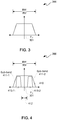
- FIG. 3 is a signal diagram depicting an exemplary embodiment of a received signal 300, such as may be received by repeater 210. Some characteristics of received signal 300 may include a signal bandwidth ("BW”) 302 and a center frequency (“F C ”) 301.
- BW signal bandwidth
- F C center frequency
- FIG. 4 is a signal diagram depicting an exemplary embodiment of another received signal 300, such as may be received by repeater 210.
- Some characteristics of this received signal 300 may include a signal bandwidth 302, a center frequency 301, a channel spacing or guard band 412, and one or more sub-bands, such as sub-bands 411-1 and 411-2 within a channel cavity 410.
- sub-bands 411-1 and 411-2 may have their own respective center frequencies 413-1 and 413-2, as well as bandwidths.
- a received signal 300 may have a number of different features depending on the type of signal transmitted.
- a basestation 201 may be coupled to another basestation and/or to one or more user devices though one or more repeaters 210.
- repeater 210 is configured to provide some deference to the type of waveform received for pre-processing for retransmission to enhance quality of such retransmitted waveform.
- waveform types include OFDM (such as for LTE or WiMax for example), spread spectrum (such as for WCDMA, TD-SCDMA or CDMA2000 for example), frequency hopping or static narrow band signals (such as for frequency hopping or static GSM, respectively, for example), or a combination thereof, among other types of waveforms or other air interface protocols.
- OFDM such as for LTE or WiMax for example
- WCDMA Wideband Code Division Multiple Access
- TD-SCDMA or CDMA2000 for example
- frequency hopping or static narrow band signals such as for frequency hopping or static GSM, respectively, for example
- communication waveforms may be analyzed, and then classified in order to provide parametric input to more accurately reproduce such original basestation 201 transmission.
- This signal analysis may be after conversion to a baseband, and this signal analysis may be used to identify a signal feature vector for providing for classification.
- a set of signal feature vectors may be extracted from communication waveforms by a signal analysis block, and each vector from such set of signal feature vectors may be provided from such signal analysis block and provided for classification by a classification block.
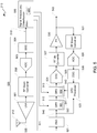
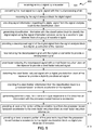
- FIG. 5 is a block diagram depicting an exemplary repeater 210.
- An over-the-air input signal may be received by receive antenna 212 of repeater 210.
- Repeater 210 in addition to one or more receive antennas 212 and one or more transmit antennas 211 as in FIG.
- LNA low noise amplifier
- RF radio frequency
- ADC analog-to-digital converter
- DDC digital down converter
- SAAC signal analysis and classification
- DUC digital up converter
- CFR crest factor reduction
- DPD digital pre-distortion
- DAC digital-to-analog converter
- An input processing chain 555 which includes one or more receive antennas 212, LNA 501, RF down converter 502, ADC 503, and optionally DDC 504, may be conventional. Accordingly, it should be appreciated that prior to delivery to an SAAC block 505, an input signal may be a down converted to baseband signal and may be digitized prior to input to SAAC block 505. However, in another configuration, a down conversion and/or digitization, including without limitation for example a portion of a spectrum of interest, may be performed by SAAC block 505.
- FIG. 6 is a block diagram depicting an exemplary SAAC block 505.
- SAAC block 505 includes a signal analysis block 610 and classification block 620.
- signal analysis block 610 may be configured as a spectral analysis block.
- repeater 210 including SAAC block 505, are further described.
- At least one receive antenna 212 of repeater 210 receives an over-the-air input signal 520 for amplification by LNA 501.
- LNA 501 provides an amplified signal to RF down converter 502 for conversion from a transmission frequency down to an IF.
- RF down converter 502 provides such amplified signal at an IF as an analog input to ADC 503 for conversion to a digital signal.
- a DDC 504 may be coupled to ADC 503 to convert such digital signal to a baseband. Whether from ADC 503 directly or from DDC 504, a digital signal 510, which is a digital version of a received over-the-air input signal 520, may be provided as an input to SAAC block 505.
- Signal analysis block 610 may be coupled to receive digital signal 510.
- Signal analysis block 610 may be coupled to provide signal information, such as spectral information or other signal information for example, regarding digital signal 510.
- Spectral analysis block 610 may be configured to provide a decomposed signal 511 as a separate output with spectral information output 611.
- Decomposed signal 511 may be a per channel decomposition of digital signal 510.
- Decomposed signal 511 may be provided as an input to DUC 521 to recompose or reconstitute digital signal 510 therefrom, as well as to up-convert such recomposed digital signal, namely to provide an IF version of digital signal 510 from decomposed signal 511 which is recomposed signal 540.
- a nondestructive implementation may be provided using parallel signal paths for digital signal 510.
- Classification block 620 may be coupled to receive signal information output 611 from signal analysis block 610. Classification block 620 may be configured to classify digital signal 510 using signal information provided from signal information output 611. Such classification may pertain to digital signal 510 being a waveform type of a group of waveform types.
- a group of waveform types may consist of orthogonal frequency division multiplexed signals, spread spectrum signals, frequency hopping band signals, static narrow band signals, and combinations thereof.
- Examples of signal information that signal analysis block 610 may be configured to provide may include: occupancy information of a band of digital signal 510; a center frequency or center frequencies of digital signal 510; a bandwidth or bandwidths of digital signal 510; a carrier frequency or carrier frequencies of digital signal 510; and/or a channel spacing or channel spacings of digital signal 510, among other specific discriminating features associated with use of a spectrum that may be used for classification.
- Occupancy information for example may include occupancy statistics of a band indicating whether two or more sub-bands are present in such band.
- Classification block 620 may be configured to detect pattern or structure of a waveform from signal information.
- classification block 620 may be configured to generate cyclostatic- or cyclostationary-based classification information, where such cyclostationary-based classification information may include a cyclic autocorrelation function ("CAF"), a cycle frequency or cycle frequencies, and/or symbol timing recovery information generated using signal information provided thereto.
- classification block 620 may be configured to perform cyclostationary operations. Additional details in waveform classification may be found in " Second-order cyclostationary of mobile WiMAX and LTE OFDM signals and application to spectrum awareness in cognitive radio systems," by A. Al-Habashna, O. A. Dobre, R. Venkatesan and D. C.
- Classification block 620 may include optional look-up tables ("LUTs") 622 for selection of parametric input corresponding to a waveform type determined. Along those lines, classification block 620 may generate classification information in response to signal information provided thereto to select parametric information stored in LUTs 622. Optionally, LUTs or other storage may be used and may be distributed in CFR block 522 and/or DPD block 524. In such an optional configuration, classification information generated by classification block 620 may be provided as sideband information to CFR block 522 and/or DPD block 524 for respective look-ups in LUTs in each of those blocks. However, for clarity, it shall be assumed that LUTs 622 are included in classification block 620.
- LUTs look-up tables
- CFR block 522 may be coupled to DUC 521 to receive therefrom a recomposed signal 540, as previously described.
- Recomposed signal 540 may additionally be provided as an input to a DPD processor 523.
- DPD block 524 may be coupled to CFR block 522 to receive therefrom a crest factor reduced version of recomposed signal 540, namely crest factor reduced signal 541.
- DPD block 524 may be configured to digitally pre-distort CFR signal 541 to provide a digitally pre-distorted signal 542 as an input to DAC 525.
- DAC 525 may convert digitally pre-distorted signal 542 to an analog signal for input to RF up converter 527 to up convert such analog signal from an IF to a transmission frequency for input to PA 530.
- PA 530 may output a to be transmitted signal 543 coupled to one or more transmit antennas 211 of FIG. 2 for retransmission of over-the-air input signal 520 after processing by repeater 210.
- Such processing may be enhanced by providing parametric input corresponding to waveform type in order to provide a high quality reproduction of an original version of over-the-air input signal 520 for such retransmission.
- Such to be transmitted signal 543 may be provided to a transmitter end (not shown for purposes of clarity) for transmission via one or more transmit antennas 211, and to an RF down converter 531 for conversion from a transmission frequency down to an IF frequency along a feedback path of repeater 210.
- Output of RF down converter 531 may be provided to ADC 528 for conversion from an analog signal to a digital signal.
- Output of ADC 528 may be provided to a DDC 526 to convert such digital signal output from ADC 528 from an IF to a baseband.
- Such baseband digital signal output from DDC 526 may be provided as an input to a DPD processor 523, and DPD processor 523 may likewise be coupled to receive recomposed signal 540.
- Output of DPD processor 523 may be provided as another input to DPD block 524.
- DPD processor 523 may be for a feedback loop for adaptation to output of PA 530.
- Classification block 620 may be coupled to CFR block 522 to provide thereto CFR parametric input via parametric input signal 512.
- CFR parametric input may include CFR parameters stored in LUTs 622 in association with corresponding waveform types.
- LUTs 622 effectively may be distributed as LUT 581 of CFR block 522 and LUT 582 of CFR block 524, as described below in additional detail.
- SAAC block 505 may include a processor-based hardware accelerator 583 coupled to receive classification information generated by classification block 620 to generate parametric input for either or both of blocks 522 and 524.
- LUTs 622 are used.
- Classification information generated by classification block 620 may be used to select such CFR parametric input for a waveform type identified.
- Examples of CFR parametric input that may vary according to waveform type may include a clipping threshold and/or a set of filter coefficients, among other CFR parameters.
- classification block 620 may be coupled to DPD block 524 to provide thereto DPD parametric input via parametric input signal 513.
- DPD parametric input may include DPD parameters stored in LUTs 622 in association with corresponding waveform types.
- CFR and DPD parametric input optionally may be stored together for same waveform types.
- Classification information generated by classification block 620 may be used to select such DPD parametric input for a waveform type identified. Examples of DPD parametric input that may vary according to waveform type may include a set of filter coefficients, and/or I and Q change values, among other DPD parameters.
- Classification block 620 may be implemented using programmable resources of FPGA 100 of FIG. 1 .
- dedicated resources and/or programmable resources may be used, whether of an FPGA, ASIC, ASSP or other type of IC.
- FPGA implementation is used.
- classification block 620 may include a microcontroller 621 configured to generate parametric input, whether CFR and/or DPD parametric input, in response to configuration information provided via classification block 620 to provide a more dynamically adaptive system.
- microcontroller 621 may be a processor-based hardware accelerator coupled to or included in classification block 620 for example to receive cyclostationary-based information and such a processor-based hardware accelerator may be configured to generate parametric input for waveform type responsive to such cyclostationary-based information.
- processor-based hardware accelerator may be coupled to CFR block 522 to provide thereto CFR parametric input signal 512 with CFR parameters, or optionally, CFR information for selection of CFR parameters by CFR block 522 may be provided via CFR parametric input signal 512.
- processor-based hardware accelerator may be coupled to DPD block 524 to provide thereto DPD parametric input signal 513 with DPD parameters, or optionally, DPD information for selection of DPD parameters by DPD block 524 may be provided via DPD parametric input signal 513.
- FIG. 7 is a flow diagram depicting an exemplary signal processing flow 700 for a repeater 210 of FIG. 5 .
- Signal processing flow 700 is further described with simultaneous reference to FIGS. 5-7 .
- Repeater 210 may include an input processing chain 555 coupled to a SAAC block 505, where SAAC block 505 may include a signal analysis block 610 and a classification block 620.
- such input signal received at 701 may be converted to a digital signal 510 by input processing chain 555.
- Signal analysis block 610 receives such digital signal 510 at 703.
- signal information may be provided regarding digital signal 510 from signal analysis block 610 to classification block 620.
- classification information may be generated with classification block to classify digital signal 510 using signal information provided as being a waveform type selected from of a group of waveform types.
- a decomposed signal 511 of digital signal 510 may be provided from signal analysis block 610 to a digital up converter 521 of repeater 210.
- decomposed signal 511 may be reconstituted with digital up converter 521 to provide a recomposed signal 540.
- recomposed signal 540 may be crest factor reduced with a CFR block 522 of repeater 210 to provide a crest factor reduced version of recomposed signal 540, namely crest factor reduced signal 541.
- crest factor reduced signal 541 may be distorted with a DPD block 524 of repeater 210 to provide a digitally pre-distorted signal 542.
- a first portion of classification information generated at 705 by classification block 620 may be provided to CFR block 522 to select crest factor reduction parametric input for a waveform type identified for an input signal received or otherwise obtained at 701.
- CFR block 522 may optionally include a LUT 581 having stored therein parametric inputs to parameterize CFR block 522 for such waveform type to enhance quality of crest factor reduced signal 541.
- Such parametric inputs may be associated with corresponding waveform types as stored in LUT 581.
- a second portion of classification information generated at 705 by classification block 620 may be provided to DPD block 524 to digital pre-distortion parametric input for such a waveform type identified.
- DPD block 524 may optionally include a LUT 582 having stored therein parametric inputs to parameterize DPD block 524 for such waveform type to enhance quality of digitally pre-distorted signal 542.
- Such parametric inputs may be associated with corresponding waveform types as stored in LUT 582.
- Such parametric inputs respectively provided to CFR block 522 and DPD block 524 may be to parameterize such blocks for an identified waveform type of a received input signal to specifically enhance quality of signals 540 and 541 respectively output from such blocks. More generally, one or more of such parametric inputs may enhance overall quality of a retransmission by repeater 210 by retransmission of a more accurate replica of an original version of such input signal.
- FIG. 8 is a flow diagram depicting another exemplary signal processing flow 800 for a repeater 210 of FIG. 5 .
- Signal processing flow 800 is further described with simultaneous reference to FIGS. 5 , 6 , and 8 .
- operations at 701 through 709 are the same as previously described with reference to FIG. 7 , such description is not repeated.
- classification information generated at 705 by classification block 620 may be provided to an optional processor-based hardware accelerator 583 of repeater 210, which optional processor-based hardware accelerator 583 may be part of SAAC 505.
- parametric input for a waveform type may be generated with processor-based hardware accelerator 583 responsive to classification information provided to such processor-based hardware accelerator 583.
- processor-based hardware accelerator 583 may be provided from processor-based hardware accelerator 583 to CFR block 522 as crest factor reduction information.
- at least another portion of such parametric input may be provided from processor-based hardware accelerator 583 to DPD block 524 as digital pre-distortion information.
- such parametric inputs provided to CFR block 522 and DPD block 524 may be to parameterize such blocks for an identified waveform type of a received input signal to specifically enhance quality of signals 540 and 541 respectively output from such blocks; however, more generally, one or more of such parametric inputs may enhance overall quality of a retransmission by repeater 210 by retransmission of a truer replica of an original version of such input signal.
- Such parametric inputs respectively provided to CFR block 522 and DPD block 524 may be to parameterize such blocks for an identified waveform type of a received input signal to specifically enhance quality of signals 540 and 541 respectively output from such blocks. More generally, one or more of such parametric inputs may enhance overall quality of a retransmission by repeater 210 by retransmission of a more accurate replica of an original version of such input signal.
Description
- The following description relates to integrated circuit devices ("ICs"). More particularly, the following description relates to a waveform differentiating repeater for an IC.
- A basestation may be coupled to another basestation or one or more user devices though a repeater. A conventional repeater accepts an incoming communication waveform and re-amplifies such incoming waveform as received. This type of repeater may be referred to as an "amplify-and-forward" repeater. Another type of repeater may digitize a received signal, process such received signal for amplification, and then re-amplify such signal for retransmission. However, conventionally such repeaters have processed all incoming signals without any deference with respect to the type of waveform received. However, there may be many types of wireless communication waveforms for a plurality of air interface protocols. Examples of waveform types include OFDM (such as for LTE or WiMax for example), spread spectrum (such as for WCDMA, TD-SCDMA or CDMA2000 for example), frequency hopping or static narrow band signals (such as for frequency hopping or static GSM, respectively, for example), or a combination thereof, among other types of waveforms or other air interface protocols. Thus, communication waveforms may have been retransmitted with such conventional repeaters without regard to type ("blind processing") leading to a significantly diminished waveform than that originally transmitted by a basestation. Such "blind processing" of a signal may mean that one or more associated signal processing algorithms may not be used. As such one or more algorithms may have a capability to improve power efficiency, such as of a power amplifier for example, and/or enhance quality or robustness of a communication link between a repeater/relay and a basestation, an inability to apply such one or more signal processing algorithms may in effect increase operational expenditures.
- Document
US 2005/254442 A1 describes a non-frequency translating repeater using a dynamic frequency detection method and repeating method. - Hence, it would be desirable to provide a repeater that provides some differentiation with respect to a type of waveform received for pre-processing for retransmission to enhance quality of such retransmitted waveform.
- An apparatus comprising the features of claim 1 and a method comprising the features of claim 10 are disclosed.
- An apparatus relates generally to a repeater. In such an apparatus, the repeater has a signal analysis and classification block. The signal analysis and classification block includes a signal analysis block and a classification block. The signal analysis block is coupled to receive a digital signal which is a digital version of an input signal received by the repeater. The signal analysis block is coupled to provide signal information regarding the digital signal to the classification block. The classification block is configured to provide classification information to classify the digital signal using the signal information provided as being a waveform type of a group of waveform types.
- In some examples, the signal information may include occupancy information of a band of the digital signal.
- In some examples, the signal information may include a center frequency of the digital signal.
- In some examples, the signal information may include a bandwidth of the digital signal.
- In some examples, the signal information may include a carrier frequency of the digital signal.
- In some examples, the signal information may include a channel spacing of the digital signal.
- In some examples, the repeater may have a digital up converter coupled to the signal analysis block and the signal analysis block may be coupled to provide a decomposed signal of the digital signal to the digital up converter.
- In some examples, the repeater may have a crest factor reduction block and a digital pre-distortion block, the signal analysis block is a spectral analysis block, the crest factor reduction block is coupled to the digital up converter to receive therefrom a recomposed signal based on an up-converted version of the decomposed signal and the digital pre-distortion block is coupled to the crest factor reduction block to receive therefrom a crest factor reduced version of the recomposed signal.
- In some examples, the classification block may be coupled to the crest factor reduction block to provide thereto the classification information to select crest factor reduction parametric input for the waveform type for use by the crest factor reduction block.
- In some examples, the classification block may be coupled to the digital pre-distortion block to provide thereto the classification information to select digital pre-distortion parametric input for the waveform type for use by the digital pre-distortion block.
- In some examples, the classification information may include cyclostationary-based information.
- In some examples, the cyclostationary-based information may be selected from a group consisting of cyclic autocorrelation information, cycle frequencies, and symbol timing recovery information.
- In some examples, the repeater may have a processor-based hardware accelerator coupled to the classification block to receive the cyclostationary-based information and the processor-based hardware accelerator is configured to generate parametric input for the waveform type responsive to the cyclostationary-based information.
- In some examples, the processor-based hardware accelerator may be coupled to the crest factor reduction block to provide thereto crest factor reduction information for the parametric input.
- In some examples, the processor-based hardware accelerator may be coupled to the digital pre-distortion block to provide thereto digital pre-distortion information for the parametric input.
- In some examples, the group of waveform types may consist of orthogonal frequency division multiplexed signals, spread spectrum signals, frequency hopping band signals, static narrow band signals, and combinations thereof.
- A method relates generally to operation of a repeater. In such a method, an input signal is received by the repeater. The repeater includes an input processing chain coupled to a signal analysis and classification block. The signal analysis and classification block includes a signal analysis block and a classification block. The input signal is converted to a digital signal with the input processing chain. The digital signal is received by the signal analysis block. Signal information regarding the digital signal is provided from the signal analysis block to the classification block. Classification information is generated with the classification block to classify the digital signal using the signal information provided as being a waveform type selected from of a group of waveform types.
- In some examples, the method may further include providing a decomposed signal of the digital signal from the signal analysis block to a digital up converter of the repeater, reconstituting the decomposed signal with the digital up converter to provide a recomposed signal, crest factor reducing the recomposed signal with a crest factor reduction block of the repeater to provide a crest factor reduced signal, distorting the crest factor reduced signal with a digital pre-distortion block of the repeater to provide a digitally pre-distorted signal, providing a first portion of the classification information from the classification block to the crest factor reduction block to select crest factor reduction parametric input for the waveform type and providing a second portion of the classification information from the classification block to the digital pre-distortion block to select digital pre-distortion parametric input for the waveform type.
- In some examples, the method may further include providing a decomposed signal of the digital signal from the signal analysis block to a digital up converter of the repeater, reconstituting the decomposed signal with the digital up converter to provide a recomposed signal, crest factor reducing the recomposed signal with a crest factor reduction block of the repeater to provide a crest factor reduced signal, distorting the crest factor reduced signal with a digital pre-distortion block of the repeater to provide a digitally pre-distorted signal, providing the classification information from the classification block to a processor-based hardware accelerator of the repeater, generating parametric input for the waveform type responsive to the classification information with the processor-based hardware accelerator and providing the parametric input from the processor-based hardware accelerator to the crest factor reduction block as crest factor reduction information.
- In some examples, the method may further include providing a decomposed signal of the digital signal from the signal analysis block to a digital up converter of the repeater, reconstituting the decomposed signal with the digital up converter to provide a recomposed signal, crest factor reducing the recomposed signal with a crest factor reduction block of the repeater to provide a crest factor reduced signal, distorting the crest factor reduced signal with a digital pre-distortion block of the repeater to provide a digitally pre-distorted signal, providing the classification information from the classification block to a processor-based hardware accelerator of the repeater, generating parametric input for the waveform type responsive to the classification information with the processor-based hardware accelerator and providing the parametric input from the processor-based hardware accelerator to the digital pre-distortion block as digital pre-distortion information.
- Accompanying drawings show exemplary apparatus(es) and/or method(s). However, the accompanying drawings should not be taken to limit the scope of the claims, but are for explanation and understanding only.
-
FIG. 1 is a simplified block diagram depicting an exemplary columnar Field Programmable Gate Array ("FPGA") architecture. -
FIG. 2 is a block diagram depicting an exemplary over-the-air ("wireless") communication system. -
FIG. 3 is a signal diagram depicting an exemplary embodiment of a received signal, such as may be received by the repeater ofFIG. 5 . -
FIG. 4 is a signal diagram depicting an exemplary embodiment of another received signal, such as may be received by the repeater ofFIG. 5 . -
FIG. 5 is a block diagram depicting an exemplary repeater. -
FIG. 6 is a block diagram depicting an exemplary signal analysis andclassification block 505. -
FIG. 7 is a flow diagram depicting an exemplary signal processing flow for the repeater ofFIG. 5 . -
FIG. 8 is a flow diagram depicting another exemplary signal processing flow for the repeater ofFIG. 5 . - In the following description, numerous specific details are set forth to provide a more thorough description of the specific examples described herein. It should be apparent, however, to one skilled in the art, that one or more other examples and/or variations of these examples may be practiced without all the specific details given below. In other instances, well known features have not been described in detail so as not to obscure the description of the examples herein. For ease of illustration, the same number labels are used in different diagrams to refer to the same items; however, in alternative examples the items may be different.
- Before describing the examples illustratively depicted in the several figures, a general introduction is provided to further understanding.
- In the past, repeaters have not provided differentiation with respect to a type of waveform received for pre-processing for retransmission. However, there are differences between types of waveforms for various air interface protocols, and these differences in effect mean that if all of such waveforms are treated the same, a lesser quality signal may be reproduced by a repeater for retransmission. More recently, a same basestation may be configured to process signals from a plurality of air interface protocols having different waveforms. Along those lines, some basestations may be configured with multi-radio access technology ("multi-RAT"). However, much of the efficiency and/or signal quality of such basestation in processing such various waveforms may be lost if a repeater is used to retransmit signals sent from such a basestation.
- As described below, a repeater is configured to adapt to waveform type of an incoming waveform. Such adaptation involves performing a signal analysis on a received signal to obtain signal information thereof, and then use such signal information obtained to classify a waveform received according to a type, such as may be associated with an air interface protocol. Informed by waveform type, parametric input may be selected or generated, such as for crest factor reduction, digital pre-distortion, or other signal processing, which is specific to the waveform type. This allows a repeater to retransmit a higher quality signal, namely a signal that more accurately represents an original transmission from a basestation.
- With the above general understanding borne in mind, various configurations for a repeater are generally described below.
- Because one or more of the above-described examples are described herein using a particular type of IC, a detailed description of such an IC is provided below. However, it should be understood that other types of ICs may benefit from one or more of the techniques described herein.
- Programmable logic devices ("PLDs") are a well-known type of integrated circuit that can be programmed to perform specified logic functions. One type of PLD, the field programmable gate array ("FPGA"), typically includes an array of programmable tiles. These programmable tiles can include, for example, input/output blocks ("lOBs"), configurable logic blocks ("CLBs"), dedicated random access memory blocks ("BRAMs"), multipliers, digital signal processing blocks ("DSPs"), processors, clock managers, delay lock loops ("DLLs"), and so forth. As used herein, "include" and "including" mean including without limitation.
- Each programmable tile typically includes both programmable interconnect and programmable logic. The programmable interconnect typically includes a large number of interconnect lines of varying lengths interconnected by programmable interconnect points ("PIPs"). The programmable logic implements the logic of a user design using programmable elements that can include, for example, function generators, registers, arithmetic logic, and so forth.
- The programmable interconnect and programmable logic are typically programmed by loading a stream of configuration data into internal configuration memory cells that define how the programmable elements are configured. The configuration data can be read from memory (e.g., from an external PROM) or written into the FPGA by an external device. The collective states of the individual memory cells then determine the function of the FPGA.
- Another type of PLD is the Complex Programmable Logic Device, or CPLD. A CPLD includes two or more "function blocks" connected together and to input/output ("I/O") resources by an interconnect switch matrix. Each function block of the CPLD includes a two-level AND/OR structure similar to those used in Programmable Logic Arrays ("PLAs") and Programmable Array Logic ("PAL") devices. In CPLDs, configuration data is typically stored on-chip in non-volatile memory. In some CPLDs, configuration data is stored on-chip in non-volatile memory, then downloaded to volatile memory as part of an initial configuration (programming) sequence.
- For all of these programmable logic devices ("PLDs"), the functionality of the device is controlled by data bits provided to the device for that purpose. The data bits can be stored in volatile memory (e.g., static memory cells, as in FPGAs and some CPLDs), in non-volatile memory (e.g., FLASH memory, as in some CPLDs), or in any other type of memory cell.
- Other PLDs are programmed by applying a processing layer, such as a metal layer, that programmably interconnects the various elements on the device. These PLDs are known as mask programmable devices. PLDs can also be implemented in other ways, e.g., using fuse or antifuse technology. The terms "PLD" and "programmable logic device" include but are not limited to these exemplary devices, as well as encompassing devices that are only partially programmable. For example, one type of PLD includes a combination of hard-coded transistor logic and a programmable switch fabric that programmably interconnects the hard-coded transistor logic.
- As noted above, advanced FPGAs can include several different types of programmable logic blocks in the array. For example,
FIG. 1 illustrates anFPGA architecture 100 that includes a large number of different programmable tiles including multi-gigabit transceivers ("MGTs") 101, configurable logic blocks ("CLBs") 102, random access memory blocks ("BRAMs") 103, input/output blocks ("lOBs") 104, configuration and clocking logic ("CONFIG/CLOCKS") 105, digital signal processing blocks ("DSPs") 106, specialized input/output blocks ("I/O") 107 (e.g., configuration ports and clock ports), and otherprogrammable logic 108 such as digital clock managers, analog-to-digital converters, system monitoring logic, and so forth. Some FPGAs also include dedicated processor blocks ("PROC") 110. - In some FPGAs, each programmable tile includes a programmable interconnect element ("INT") 111 having standardized connections to and from a corresponding interconnect element in each adjacent tile. Therefore, the programmable interconnect elements taken together implement the programmable interconnect structure for the illustrated FPGA. The
programmable interconnect element 111 also includes the connections to and from the programmable logic element within the same tile, as shown by the examples included at the top ofFIG. 1 . - For example, a
CLB 102 can include a configurable logic element ("CLE") 112 that can be programmed to implement user logic plus a single programmable interconnect element ("INT") 111. ABRAM 103 can include a BRAM logic element ("BRL") 113 in addition to one or more programmable interconnect elements. Typically, the number of interconnect elements included in a tile depends on the height of the tile. In the pictured embodiment, a BRAM tile has the same height as five CLBs, but other numbers (e.g., four) can also be used. ADSP tile 106 can include a DSP logic element ("DSPL") 114 in addition to an appropriate number of programmable interconnect elements. AnIOB 104 can include, for example, two instances of an input/output logic element ("IOL") 115 in addition to one instance of theprogrammable interconnect element 111. As will be clear to those of skill in the art, the actual I/O pads connected, for example, to the I/O logic element 115 typically are not confined to the area of the input/output logic element 115. - In the pictured embodiment, a horizontal area near the center of the die (shown in
FIG. 1 ) is used for configuration, clock, and other control logic. Vertical columns 109 extending from this horizontal area or column are used to distribute the clocks and configuration signals across the breadth of the FPGA. - Some FPGAs utilizing the architecture illustrated in
FIG. 1 include additional logic blocks that disrupt the regular columnar structure making up a large part of the FPGA. The additional logic blocks can be programmable blocks and/or dedicated logic. For example,processor block 110 spans several columns of CLBs and BRAMs. - Note that
FIG. 1 is intended to illustrate only an exemplary FPGA architecture. For example, the numbers of logic blocks in a row, the relative width of the rows, the number and order of rows, the types of logic blocks included in the rows, the relative sizes of the logic blocks, and the interconnect/logic implementations included at the top ofFIG. 1 are purely exemplary. For example, in an actual FPGA more than one adjacent row of CLBs is typically included wherever the CLBs appear, to facilitate the efficient implementation of user logic, but the number of adjacent CLB rows varies with the overall size of the FPGA. -
FIG. 2 is a block diagram depicting an exemplary over-the-air ("wireless")communication system 200.Communication system 200 includes abasestation 201 and arepeater 210.Basestation 201 has one or more transmitantennas 202.Repeater 210 has one or more receiveantennas 212 coupled to such one or more transmitantennas 202 through awireless uplink 203.Repeater 210 is configured to retransmit transmissions sent frombasestation 201 torepeater 210 viauplink 203.Repeater 210 may retransmit such transmissions via one or more receive transmitantennas 211 ofrepeater 210, such as for anotherwireless uplink 213. -
FIG. 3 is a signal diagram depicting an exemplary embodiment of a receivedsignal 300, such as may be received byrepeater 210. Some characteristics of receivedsignal 300 may include a signal bandwidth ("BW") 302 and a center frequency ("FC") 301. -
FIG. 4 is a signal diagram depicting an exemplary embodiment of another receivedsignal 300, such as may be received byrepeater 210. Some characteristics of this receivedsignal 300 may include asignal bandwidth 302, acenter frequency 301, a channel spacing orguard band 412, and one or more sub-bands, such as sub-bands 411-1 and 411-2 within achannel cavity 410. Moreover, sub-bands 411-1 and 411-2 may have their own respective center frequencies 413-1 and 413-2, as well as bandwidths. - Along the above lines of
FIGS. 2 through 4 , a receivedsignal 300 may have a number of different features depending on the type of signal transmitted. Abasestation 201 may be coupled to another basestation and/or to one or more user devices though one ormore repeaters 210. Rather than processing all incoming signals the same without any deference with respect to the type of waveform received,repeater 210 is configured to provide some deference to the type of waveform received for pre-processing for retransmission to enhance quality of such retransmitted waveform. However, there may be many types of wireless communication waveforms for a plurality of air interface protocols. Examples of waveform types include OFDM (such as for LTE or WiMax for example), spread spectrum (such as for WCDMA, TD-SCDMA or CDMA2000 for example), frequency hopping or static narrow band signals (such as for frequency hopping or static GSM, respectively, for example), or a combination thereof, among other types of waveforms or other air interface protocols. Thus, to retransmit a receivedsignal 300 with regard to waveform type in order to provide a high-quality retransmission, namely a retransmission of a receivedsignal 300 more closely comporting to an original form of an originally transmitted version of same by abasestation 201, communication waveforms may be analyzed, and then classified in order to provide parametric input to more accurately reproduce suchoriginal basestation 201 transmission. This signal analysis may be after conversion to a baseband, and this signal analysis may be used to identify a signal feature vector for providing for classification. Along those lines, a set of signal feature vectors may be extracted from communication waveforms by a signal analysis block, and each vector from such set of signal feature vectors may be provided from such signal analysis block and provided for classification by a classification block. - To provide such a high-quality retransmission, a
repeater 210 capable of identifying input waveform type for selecting and/or generating parametric input corresponding thereto may be used.FIG. 5 is a block diagram depicting anexemplary repeater 210. An over-the-air input signal may be received by receiveantenna 212 ofrepeater 210.Repeater 210, in addition to one or more receiveantennas 212 and one or more transmitantennas 211 as inFIG. 2 , may further include a low noise amplifier ("LNA") 501, a radio frequency ("RF") downconverter 502 for conversion from a transmission frequency down to an intermediate frequency ("IF"), an analog-to-digital converter ("ADC") 503, a digital down converter ("DDC") 504 for conversion down to a baseband frequency ("baseband"), a signal analysis and classification ("SAAC") block 505, a digital up converter ("DUC") 521 for conversion up to an IF, a crest factor reduction ("CFR") block 522, a digital pre-distortion ("DPD") block 524, aDPD processor 523, a digital-to-analog converter ("DAC") 525, an RF upconverter 527 for conversion up to a transmission frequency, aDDC 526, a power amplifier ("PA") 530 including a pre-amp, anADC 528, and an RF downconverter 531 for conversion down to an IF. Aninput processing chain 555, which includes one or more receiveantennas 212,LNA 501, RF downconverter 502,ADC 503, and optionallyDDC 504, may be conventional. Accordingly, it should be appreciated that prior to delivery to anSAAC block 505, an input signal may be a down converted to baseband signal and may be digitized prior to input to SAAC block 505. However, in another configuration, a down conversion and/or digitization, including without limitation for example a portion of a spectrum of interest, may be performed bySAAC block 505. -
FIG. 6 is a block diagram depicting anexemplary SAAC block 505.SAAC block 505 includes asignal analysis block 610 andclassification block 620. In an example,signal analysis block 610 may be configured as a spectral analysis block. With simultaneous reference toFIGS. 5 and6 ,repeater 210, includingSAAC block 505, are further described. - At least one receive
antenna 212 ofrepeater 210 receives an over-the-air input signal 520 for amplification byLNA 501.LNA 501 provides an amplified signal to RF downconverter 502 for conversion from a transmission frequency down to an IF. RF downconverter 502 provides such amplified signal at an IF as an analog input toADC 503 for conversion to a digital signal. ADDC 504 may be coupled toADC 503 to convert such digital signal to a baseband. Whether fromADC 503 directly or fromDDC 504, adigital signal 510, which is a digital version of a received over-the-air input signal 520, may be provided as an input to SAAC block 505. -
Signal analysis block 610 may be coupled to receivedigital signal 510.Signal analysis block 610 may be coupled to provide signal information, such as spectral information or other signal information for example, regardingdigital signal 510.Spectral analysis block 610 may be configured to provide a decomposedsignal 511 as a separate output withspectral information output 611. - Decomposed
signal 511 may be a per channel decomposition ofdigital signal 510. Decomposedsignal 511 may be provided as an input toDUC 521 to recompose or reconstitutedigital signal 510 therefrom, as well as to up-convert such recomposed digital signal, namely to provide an IF version ofdigital signal 510 from decomposedsignal 511 which is recomposedsignal 540. This presumes thatspectral analysis block 610 performs some degree of destructive testing ondigital signal 510. However, in another configuration, a nondestructive implementation may be provided using parallel signal paths fordigital signal 510. -
Classification block 620 may be coupled to receivesignal information output 611 fromsignal analysis block 610.Classification block 620 may be configured to classifydigital signal 510 using signal information provided fromsignal information output 611. Such classification may pertain todigital signal 510 being a waveform type of a group of waveform types. A group of waveform types may consist of orthogonal frequency division multiplexed signals, spread spectrum signals, frequency hopping band signals, static narrow band signals, and combinations thereof. - Examples of signal information that signal
analysis block 610 may be configured to provide may include: occupancy information of a band ofdigital signal 510; a center frequency or center frequencies ofdigital signal 510; a bandwidth or bandwidths ofdigital signal 510; a carrier frequency or carrier frequencies ofdigital signal 510; and/or a channel spacing or channel spacings ofdigital signal 510, among other specific discriminating features associated with use of a spectrum that may be used for classification. Occupancy information for example may include occupancy statistics of a band indicating whether two or more sub-bands are present in such band. -
Classification block 620 may be configured to detect pattern or structure of a waveform from signal information. For example,classification block 620 may be configured to generate cyclostatic- or cyclostationary-based classification information, where such cyclostationary-based classification information may include a cyclic autocorrelation function ("CAF"), a cycle frequency or cycle frequencies, and/or symbol timing recovery information generated using signal information provided thereto. Along those lines,classification block 620 may be configured to perform cyclostationary operations. Additional details in waveform classification may be found in "Second-order cyclostationary of mobile WiMAX and LTE OFDM signals and application to spectrum awareness in cognitive radio systems," by A. Al-Habashna, O. A. Dobre, R. Venkatesan and D. C. Popescu, published in IEEE J. of Selected topics in signal processing, Vol. 6, No. 1 February 2012, pp. 26-42, for classification of LTE OFDM signals. Other operations that may be performed may be for identifying and classifying CDMA signals, such as in "A detection method of WCDMA signal based on quadratic fourth-order moment chip at lower SNR", by P. Junjie and Z. Zhijin, Wireless Communications, Networking and Mobile Computing, 2009, WiCom '09. As there are many types of waveforms for various over-the-air protocols, a complete list of all possible waveform operations is not described herein in unnecessary detail for purposes of clarity and not limitation. -
Classification block 620 may include optional look-up tables ("LUTs") 622 for selection of parametric input corresponding to a waveform type determined. Along those lines,classification block 620 may generate classification information in response to signal information provided thereto to select parametric information stored inLUTs 622. Optionally, LUTs or other storage may be used and may be distributed in CFR block 522 and/orDPD block 524. In such an optional configuration, classification information generated byclassification block 620 may be provided as sideband information to CFR block 522 and/or DPD block 524 for respective look-ups in LUTs in each of those blocks. However, for clarity, it shall be assumed thatLUTs 622 are included inclassification block 620. - CFR block 522 may be coupled to
DUC 521 to receive therefrom a recomposedsignal 540, as previously described.Recomposed signal 540 may additionally be provided as an input to aDPD processor 523. DPD block 524 may be coupled to CFR block 522 to receive therefrom a crest factor reduced version of recomposedsignal 540, namely crest factor reducedsignal 541. DPD block 524 may be configured to digitally pre-distort CFR signal 541 to provide a digitallypre-distorted signal 542 as an input toDAC 525.DAC 525 may convert digitallypre-distorted signal 542 to an analog signal for input to RF upconverter 527 to up convert such analog signal from an IF to a transmission frequency for input toPA 530.PA 530 may output a to be transmittedsignal 543 coupled to one or more transmitantennas 211 ofFIG. 2 for retransmission of over-the-air input signal 520 after processing byrepeater 210. Such processing may be enhanced by providing parametric input corresponding to waveform type in order to provide a high quality reproduction of an original version of over-the-air input signal 520 for such retransmission. - Such to be transmitted
signal 543 may be provided to a transmitter end (not shown for purposes of clarity) for transmission via one or more transmitantennas 211, and to an RF downconverter 531 for conversion from a transmission frequency down to an IF frequency along a feedback path ofrepeater 210. Output of RF downconverter 531 may be provided toADC 528 for conversion from an analog signal to a digital signal. Output ofADC 528 may be provided to aDDC 526 to convert such digital signal output fromADC 528 from an IF to a baseband. Such baseband digital signal output fromDDC 526 may be provided as an input to aDPD processor 523, andDPD processor 523 may likewise be coupled to receive recomposedsignal 540. Output ofDPD processor 523 may be provided as another input to DPD block 524.DPD processor 523 may be for a feedback loop for adaptation to output ofPA 530. -
Classification block 620 may be coupled to CFR block 522 to provide thereto CFR parametric input viaparametric input signal 512. Such CFR parametric input may include CFR parameters stored inLUTs 622 in association with corresponding waveform types. Optionally, in another implementation,LUTs 622 effectively may be distributed asLUT 581 of CFR block 522 andLUT 582 of CFR block 524, as described below in additional detail. Furthermore, optionally SAAC block 505 may include a processor-basedhardware accelerator 583 coupled to receive classification information generated byclassification block 620 to generate parametric input for either or both ofblocks LUTs 622 are used. - Classification information generated by
classification block 620 may be used to select such CFR parametric input for a waveform type identified. Examples of CFR parametric input that may vary according to waveform type may include a clipping threshold and/or a set of filter coefficients, among other CFR parameters. - Optionally or additionally,
classification block 620 may be coupled to DPD block 524 to provide thereto DPD parametric input viaparametric input signal 513. Such DPD parametric input may include DPD parameters stored inLUTs 622 in association with corresponding waveform types. CFR and DPD parametric input optionally may be stored together for same waveform types. Classification information generated byclassification block 620 may be used to select such DPD parametric input for a waveform type identified. Examples of DPD parametric input that may vary according to waveform type may include a set of filter coefficients, and/or I and Q change values, among other DPD parameters. -
Classification block 620, as well assignal analysis block 610, may be implemented using programmable resources ofFPGA 100 ofFIG. 1 . However, in other implementations, dedicated resources and/or programmable resources may be used, whether of an FPGA, ASIC, ASSP or other type of IC. However, for purposes of clarity and not limitation, it shall be assumed that an FPGA implementation is used. - Optionally,
classification block 620 may include a microcontroller 621 configured to generate parametric input, whether CFR and/or DPD parametric input, in response to configuration information provided viaclassification block 620 to provide a more dynamically adaptive system. Along those lines, microcontroller 621 may be a processor-based hardware accelerator coupled to or included inclassification block 620 for example to receive cyclostationary-based information and such a processor-based hardware accelerator may be configured to generate parametric input for waveform type responsive to such cyclostationary-based information. Along those lines, such processor-based hardware accelerator may be coupled to CFR block 522 to provide thereto CFRparametric input signal 512 with CFR parameters, or optionally, CFR information for selection of CFR parameters by CFR block 522 may be provided via CFRparametric input signal 512. Likewise, such processor-based hardware accelerator may be coupled to DPD block 524 to provide thereto DPDparametric input signal 513 with DPD parameters, or optionally, DPD information for selection of DPD parameters byDPD block 524 may be provided via DPDparametric input signal 513. -
FIG. 7 is a flow diagram depicting an exemplarysignal processing flow 700 for arepeater 210 ofFIG. 5 .Signal processing flow 700 is further described with simultaneous reference toFIGS. 5-7 . - At 701, an input signal is received by
repeater 210.Repeater 210 may include aninput processing chain 555 coupled to aSAAC block 505, where SAAC block 505 may include asignal analysis block 610 and aclassification block 620. - At 702, such input signal received at 701 may be converted to a
digital signal 510 byinput processing chain 555.Signal analysis block 610 receives suchdigital signal 510 at 703. At 704, signal information may be provided regardingdigital signal 510 fromsignal analysis block 610 toclassification block 620. At 705, classification information may be generated with classification block to classifydigital signal 510 using signal information provided as being a waveform type selected from of a group of waveform types. - At 706, a decomposed
signal 511 ofdigital signal 510 may be provided fromsignal analysis block 610 to a digital upconverter 521 ofrepeater 210. At 707, decomposedsignal 511 may be reconstituted with digital upconverter 521 to provide a recomposedsignal 540. At 708, recomposedsignal 540 may be crest factor reduced with aCFR block 522 ofrepeater 210 to provide a crest factor reduced version of recomposedsignal 540, namely crest factor reducedsignal 541. At 709, crest factor reducedsignal 541 may be distorted with aDPD block 524 ofrepeater 210 to provide a digitallypre-distorted signal 542. - Optionally, at 710 a first portion of classification information generated at 705 by
classification block 620 may be provided to CFR block 522 to select crest factor reduction parametric input for a waveform type identified for an input signal received or otherwise obtained at 701. Along those lines, CFR block 522 may optionally include aLUT 581 having stored therein parametric inputs to parameterize CFR block 522 for such waveform type to enhance quality of crest factor reducedsignal 541. Such parametric inputs may be associated with corresponding waveform types as stored inLUT 581. - Optionally, at 711 a second portion of classification information generated at 705 by
classification block 620 may be provided to DPD block 524 to digital pre-distortion parametric input for such a waveform type identified. Along those lines, DPD block 524 may optionally include aLUT 582 having stored therein parametric inputs to parameterize DPD block 524 for such waveform type to enhance quality of digitallypre-distorted signal 542. Such parametric inputs may be associated with corresponding waveform types as stored inLUT 582. - Such parametric inputs respectively provided to CFR block 522 and DPD block 524 may be to parameterize such blocks for an identified waveform type of a received input signal to specifically enhance quality of
signals repeater 210 by retransmission of a more accurate replica of an original version of such input signal. -
FIG. 8 is a flow diagram depicting another exemplarysignal processing flow 800 for arepeater 210 ofFIG. 5 .Signal processing flow 800 is further described with simultaneous reference toFIGS. 5 ,6 , and8 . As operations at 701 through 709 are the same as previously described with reference toFIG. 7 , such description is not repeated. - At 810, classification information generated at 705 by
classification block 620 may be provided to an optional processor-basedhardware accelerator 583 ofrepeater 210, which optional processor-basedhardware accelerator 583 may be part ofSAAC 505. At 811, parametric input for a waveform type may be generated with processor-basedhardware accelerator 583 responsive to classification information provided to such processor-basedhardware accelerator 583. At 812, at least a portion of such parametric input may be provided from processor-basedhardware accelerator 583 to CFR block 522 as crest factor reduction information. At 813, at least another portion of such parametric input may be provided from processor-basedhardware accelerator 583 to DPD block 524 as digital pre-distortion information. - Again, such parametric inputs provided to CFR block 522 and DPD block 524 may be to parameterize such blocks for an identified waveform type of a received input signal to specifically enhance quality of
signals repeater 210 by retransmission of a truer replica of an original version of such input signal. Such parametric inputs respectively provided to CFR block 522 and DPD block 524 may be to parameterize such blocks for an identified waveform type of a received input signal to specifically enhance quality ofsignals repeater 210 by retransmission of a more accurate replica of an original version of such input signal.
Claims (12)
- An apparatus, comprising:a repeater (210) having a signal analysis and classification block (505);wherein the signal analysis and classification block (505) comprises a signal analysis block (610) and a classification block (620);wherein the signal analysis block (610) is configured to receive a digital signal which is a digital version of an input signal received by the repeater (210);wherein the signal analysis block (610) is configured to provide signal information regarding the digital signal to the classification block (620);wherein the classification block (620) is configured to provide classification information to classify the digital signal using the signal information provided as being a waveform type of a group of waveform types; andwherein the classification block (620) is coupled to at least one of a crest factor reduction block (522) or a digital pre-distortion block (524) configured to provide the classification information for selecting parametric input based on the waveform type.
- The apparatus according to claim 1, wherein:the repeater (210) has a digital up converter (521) coupled to the signal analysis block (610); andthe signal analysis block (610) is configured to provide a decomposed signal of the digital signal to the digital up converter (521).
- The apparatus according to claim 2, wherein:the repeater (210) has the crest factor reduction block (522) and the digital pre-distortion block (524);the signal analysis block (610) is a spectral analysis block;the crest factor reduction block (522) is coupled to the digital up converter (521) and is configured to receive therefrom a recomposed signal based on an up-converted version of the decomposed signal; andthe digital pre-distortion block (524) is coupled to the crest factor reduction block (522) to receive therefrom a crest factor reduced version of the recomposed signal.
- The apparatus according to claim 3, wherein the classification block (620) is coupled to the crest factor reduction block (522) to provide thereto the classification information to select the parametric input for the waveform type for use by the crest factor reduction block (522).
- The apparatus according to claim 3, wherein the classification block (620) is coupled to the digital pre-distortion block (524) to provide thereto the classification information to select the parametric input for the waveform type for use by the digital pre-distortion block (524).
- The apparatus according to claim 3, wherein the classification information includes cyclostationary-based information.
- The apparatus according to claim 6, wherein the cyclostationary-based information is selected from a group consisting of cyclic autocorrelation information, cycle frequencies, and symbol timing recovery information.
- The apparatus according to claim 6, wherein the group of waveform types consists of orthogonal frequency division multiplexed signals, spread spectrum signals, frequency hopping band signals, static narrow band signals, and combinations thereof.
- The apparatus according to any of claims 1-8, wherein the signal information includes occupancy information of a band of the digital signal, a center frequency of the digital signal, a bandwidth of the digital signal, a carrier frequency of the digital signal, or a channel spacing of the digital signal.
- A method (700), performed by an apparatus comprising a repeater,
comprising:receiving (701) an input signal by the repeater (210);wherein the repeater (210) comprises an input processing chain (555) coupled to a signal analysis and classification block (620);wherein the signal analysis and classification block (620) comprises a signal analysis block (610) and a classification block (620);converting (702) the input signal to a digital signal with the input processing chain (555);receiving (703) by the signal analysis block (610) the digital signal;providing (704) signal information regarding the digital signal from the signal analysis block (610) to the classification block (620);generating (705) classification information with the classification block (620) to classify the digital signal using the signal information provided as being a waveform type selected from of a group of waveform types; andselecting (710, 711) parametric input, for at least one of a crest factor reduction block (522) or a digital pre-distortion block (524), for the waveform type using the classification information. - The method (700) according to claim 10, further comprising:providing (706) a decomposed signal of the digital signal from the signal analysis block (610) to a digital up converter (521) of the repeater (210);reconstituting (707) the decomposed signal with the digital up converter (521) to provide a recomposed signal;crest factor reducing (708) the recomposed signal with the crest factor reduction block (522) of the repeater (210) to provide a crest factor reduced signal;distorting (709) the crest factor reduced signal with the digital pre-distortion block (524) of the repeater (210) to provide a digitally pre-distorted signal;providing (710) a first portion of the classification information from the classification block (620) to the crest factor reduction block (522) to select the parametric input for crest factor reduction for the waveform type; andproviding (711) a second portion of the classification information from the classification block (620) to the digital pre-distortion block (524) to select the parametric input for digital pre-distortion for the waveform type.
- The method (700) according to claim 10, further comprising:providing (706) a decomposed signal of the digital signal from the signal analysis block (610) to a digital up converter (521) of the repeater (210);reconstituting (707) the decomposed signal with the digital up converter (521) to provide a recomposed signal;crest factor reducing (708) the recomposed signal with the crest factor reduction block (522) of the repeater (210) to provide a crest factor reduced signal;distorting (709) the crest factor reduced signal with the digital pre-distortion block (524) of the repeater (210) to provide a digitally pre-distorted signal;providing (810) the classification information from the classification block (620) to a processor-based hardware accelerator (583) of the repeater (210);generating (811) the parametric input for the waveform type responsive to the classification information with the processor-based hardware accelerator (583); andproviding (812, 813) the parametric input generated from the processor-based hardware accelerator (583) to the crest factor reduction block (522) as crest factor reduction information or to the digital pre-distortion block (524) as digital pre-distortion information.
Applications Claiming Priority (2)
| Application Number | Priority Date | Filing Date | Title |
|---|---|---|---|
| US14/267,846 US9008156B1 (en) | 2014-05-01 | 2014-05-01 | Waveform differentiating repeater |
| PCT/US2015/019490 WO2015167669A1 (en) | 2014-05-01 | 2015-03-09 | Waveform differentiating repeater |
Publications (2)
| Publication Number | Publication Date |
|---|---|
| EP3141078A1 EP3141078A1 (en) | 2017-03-15 |
| EP3141078B1 true EP3141078B1 (en) | 2019-10-16 |
Family
ID=52782298
Family Applications (1)
| Application Number | Title | Priority Date | Filing Date |
|---|---|---|---|
| EP15714994.9A Active EP3141078B1 (en) | 2014-05-01 | 2015-03-09 | Waveform differentiating repeater |
Country Status (6)
| Country | Link |
|---|---|
| US (1) | US9008156B1 (en) |
| EP (1) | EP3141078B1 (en) |
| JP (1) | JP6337148B2 (en) |
| KR (1) | KR102119924B1 (en) |
| CN (1) | CN106464216B (en) |
| WO (1) | WO2015167669A1 (en) |
Families Citing this family (7)
| Publication number | Priority date | Publication date | Assignee | Title |
|---|---|---|---|---|
| US9455760B1 (en) * | 2015-07-02 | 2016-09-27 | Xilinx, Inc. | Waveform adaptable digital predistortion |
| US9338039B1 (en) | 2015-08-26 | 2016-05-10 | Xilinx, Inc. | Efficient signal classification in digital pre-distortion systems |
| US9847802B1 (en) * | 2016-08-16 | 2017-12-19 | Xilinx, Inc. | Reconfiguration of single-band transmit and receive paths to multi-band transmit and receive paths in an integrated circuit |
| KR20210063368A (en) * | 2018-09-26 | 2021-06-01 | 자일링크스 인코포레이티드 | Crest factor reduction method for cable TV amplifier and circuit therefor |
| CN109982253A (en) * | 2019-01-29 | 2019-07-05 | 中国航空无线电电子研究所 | Waveform weighted platform based on radio multiple correlation characteristic |
| WO2021188792A1 (en) * | 2020-03-18 | 2021-09-23 | Commscope Technologies Llc | Single-chip digital pre-distortion (dpd) device implemented using radio frequency transceiver integrated circuit with integrated dpd function |
| US11888670B1 (en) * | 2022-07-20 | 2024-01-30 | Qualcomm Incorporated | Over the air reliable digital pre-distortion |
Family Cites Families (13)
| Publication number | Priority date | Publication date | Assignee | Title |
|---|---|---|---|---|
| JP3075846B2 (en) * | 1991-06-28 | 2000-08-14 | 三菱電機株式会社 | General-purpose demodulator and communication waveform analyzer |
| US5544661A (en) * | 1994-01-13 | 1996-08-13 | Charles L. Davis | Real time ambulatory patient monitor |
| WO2005115022A2 (en) * | 2004-05-13 | 2005-12-01 | Widefi, Inc. | Non-frequency translating repeater with detection and media access control |
| US8654868B2 (en) * | 2006-04-18 | 2014-02-18 | Qualcomm Incorporated | Offloaded processing for wireless applications |
| US7970542B2 (en) * | 2007-04-17 | 2011-06-28 | Toa Systems, Inc. | Method of detecting, locating, and classifying lightning |
| WO2010088110A2 (en) * | 2009-01-30 | 2010-08-05 | Yu, Mukwan | Amplification system for interference suppression in wireless communications |
| WO2010124297A1 (en) * | 2009-04-24 | 2010-10-28 | Dali Systems Co.Ltd. | Remotely reconfigurable power amplifier system and method |
| US20130070651A1 (en) * | 2010-05-27 | 2013-03-21 | Kyocera Corporation | Power line communication device, security level setting method, and storage medium storing security level setting program |
| CA2814825C (en) * | 2010-10-15 | 2016-11-22 | Lgch, Inc. | Method and apparatus for detecting seizures |
| JP5647871B2 (en) * | 2010-11-19 | 2015-01-07 | 日本放送協会 | OFDM signal retransmission apparatus |
| KR101237490B1 (en) * | 2011-05-03 | 2013-02-27 | 인텔라 주식회사 | the performance analysis and self diagnosis device for the RF system of mobile telecommunication |
| US8837633B2 (en) * | 2011-10-21 | 2014-09-16 | Xilinx, Inc. | Systems and methods for digital processing based on active signal channels of a communication system |
| CN103248458A (en) * | 2013-05-11 | 2013-08-14 | 哈尔滨工业大学深圳研究生院 | Physical layer network coding system and method based on FQPSK modulation |
-
2014
- 2014-05-01 US US14/267,846 patent/US9008156B1/en active Active
-
2015
- 2015-03-09 WO PCT/US2015/019490 patent/WO2015167669A1/en active Application Filing
- 2015-03-09 EP EP15714994.9A patent/EP3141078B1/en active Active
- 2015-03-09 CN CN201580023539.1A patent/CN106464216B/en active Active
- 2015-03-09 KR KR1020167033249A patent/KR102119924B1/en active IP Right Grant
- 2015-03-09 JP JP2016565434A patent/JP6337148B2/en active Active
Non-Patent Citations (1)
| Title |
|---|
| None * |
Also Published As
| Publication number | Publication date |
|---|---|
| WO2015167669A8 (en) | 2016-11-10 |
| CN106464216A (en) | 2017-02-22 |
| US9008156B1 (en) | 2015-04-14 |
| KR20170003594A (en) | 2017-01-09 |
| WO2015167669A1 (en) | 2015-11-05 |
| KR102119924B1 (en) | 2020-06-05 |
| JP6337148B2 (en) | 2018-06-06 |
| EP3141078A1 (en) | 2017-03-15 |
| JP2017520950A (en) | 2017-07-27 |
| CN106464216B (en) | 2018-06-01 |
Similar Documents
| Publication | Publication Date | Title |
|---|---|---|
| EP3141078B1 (en) | Waveform differentiating repeater | |
| EP3314837B1 (en) | Waveform adaptable digital predistortion | |
| US9590567B2 (en) | Moving mean and magnitude dual path digital predistortion | |
| EP3072233B1 (en) | Multi-path digital pre-distortion | |
| CN109983693B (en) | Method and circuit for predistortion of a power amplifier | |
| US9608672B2 (en) | Apparatus and method for generating base band receive signals | |
| KR101752040B1 (en) | Systems and methods for digital processing based on active signal channels of a communication system | |
| WO2016095528A1 (en) | Digital predistortion method and apparatus, and computer storage medium | |
| US9485129B1 (en) | Multi-standard peak canceling circuitry | |
| US10944444B2 (en) | Method of and circuit for predistortion for a cable TV amplifier | |
| US10181867B2 (en) | Crest factor reduction in a radio transmitter | |
| US9025691B1 (en) | Channel equalization | |
| CN102801670B (en) | A kind of digital pre-distortion method and system | |
| Zhang et al. | A 30 Gbps low-complexity and real-time digital modem for wireless communications at 0.325 THz | |
| WO2018137184A1 (en) | Signal processing method and device | |
| Yu et al. | A reconfigurable in-band digital predistortion technique for mmWave power amplifiers excited by a signal with 640 MHz modulation bandwidth | |
| US9712348B1 (en) | System, device, and method for shaping transmit noise | |
| Omara | Efficient design of Dual Digital Up Converter for WCDMA and CDMA2000 using system generator | |
| KR101193936B1 (en) | Signal processing circuit |
Legal Events
| Date | Code | Title | Description |
|---|---|---|---|
| STAA | Information on the status of an ep patent application or granted ep patent |
Free format text: STATUS: THE INTERNATIONAL PUBLICATION HAS BEEN MADE |
|
| PUAI | Public reference made under article 153(3) epc to a published international application that has entered the european phase |
Free format text: ORIGINAL CODE: 0009012 |
|
| STAA | Information on the status of an ep patent application or granted ep patent |
Free format text: STATUS: REQUEST FOR EXAMINATION WAS MADE |
|
| 17P | Request for examination filed |
Effective date: 20161201 |
|
| AK | Designated contracting states |
Kind code of ref document: A1 Designated state(s): AL AT BE BG CH CY CZ DE DK EE ES FI FR GB GR HR HU IE IS IT LI LT LU LV MC MK MT NL NO PL PT RO RS SE SI SK SM TR |
|
| AX | Request for extension of the european patent |
Extension state: BA ME |
|
| DAV | Request for validation of the european patent (deleted) | ||
| DAX | Request for extension of the european patent (deleted) | ||
| STAA | Information on the status of an ep patent application or granted ep patent |
Free format text: STATUS: EXAMINATION IS IN PROGRESS |
|
| 17Q | First examination report despatched |
Effective date: 20180831 |
|
| GRAP | Despatch of communication of intention to grant a patent |
Free format text: ORIGINAL CODE: EPIDOSNIGR1 |
|
| STAA | Information on the status of an ep patent application or granted ep patent |
Free format text: STATUS: GRANT OF PATENT IS INTENDED |
|
| INTG | Intention to grant announced |
Effective date: 20190507 |
|
| GRAS | Grant fee paid |
Free format text: ORIGINAL CODE: EPIDOSNIGR3 |
|
| GRAA | (expected) grant |
Free format text: ORIGINAL CODE: 0009210 |
|
| STAA | Information on the status of an ep patent application or granted ep patent |
Free format text: STATUS: THE PATENT HAS BEEN GRANTED |
|
| AK | Designated contracting states |
Kind code of ref document: B1 Designated state(s): AL AT BE BG CH CY CZ DE DK EE ES FI FR GB GR HR HU IE IS IT LI LT LU LV MC MK MT NL NO PL PT RO RS SE SI SK SM TR |
|
| REG | Reference to a national code |
Ref country code: GB Ref legal event code: FG4D |
|
| REG | Reference to a national code |
Ref country code: CH Ref legal event code: EP |
|
| REG | Reference to a national code |
Ref country code: DE Ref legal event code: R096 Ref document number: 602015039872 Country of ref document: DE |
|
| REG | Reference to a national code |
Ref country code: IE Ref legal event code: FG4D |
|
| REG | Reference to a national code |
Ref country code: AT Ref legal event code: REF Ref document number: 1192592 Country of ref document: AT Kind code of ref document: T Effective date: 20191115 |
|
| REG | Reference to a national code |
Ref country code: NL Ref legal event code: MP Effective date: 20191016 |
|
| REG | Reference to a national code |
Ref country code: LT Ref legal event code: MG4D |
|
| REG | Reference to a national code |
Ref country code: AT Ref legal event code: MK05 Ref document number: 1192592 Country of ref document: AT Kind code of ref document: T Effective date: 20191016 |
|
| PG25 | Lapsed in a contracting state [announced via postgrant information from national office to epo] |
Ref country code: PL Free format text: LAPSE BECAUSE OF FAILURE TO SUBMIT A TRANSLATION OF THE DESCRIPTION OR TO PAY THE FEE WITHIN THE PRESCRIBED TIME-LIMIT Effective date: 20191016 Ref country code: LT Free format text: LAPSE BECAUSE OF FAILURE TO SUBMIT A TRANSLATION OF THE DESCRIPTION OR TO PAY THE FEE WITHIN THE PRESCRIBED TIME-LIMIT Effective date: 20191016 Ref country code: SE Free format text: LAPSE BECAUSE OF FAILURE TO SUBMIT A TRANSLATION OF THE DESCRIPTION OR TO PAY THE FEE WITHIN THE PRESCRIBED TIME-LIMIT Effective date: 20191016 Ref country code: LV Free format text: LAPSE BECAUSE OF FAILURE TO SUBMIT A TRANSLATION OF THE DESCRIPTION OR TO PAY THE FEE WITHIN THE PRESCRIBED TIME-LIMIT Effective date: 20191016 Ref country code: NL Free format text: LAPSE BECAUSE OF FAILURE TO SUBMIT A TRANSLATION OF THE DESCRIPTION OR TO PAY THE FEE WITHIN THE PRESCRIBED TIME-LIMIT Effective date: 20191016 Ref country code: NO Free format text: LAPSE BECAUSE OF FAILURE TO SUBMIT A TRANSLATION OF THE DESCRIPTION OR TO PAY THE FEE WITHIN THE PRESCRIBED TIME-LIMIT Effective date: 20200116 Ref country code: GR Free format text: LAPSE BECAUSE OF FAILURE TO SUBMIT A TRANSLATION OF THE DESCRIPTION OR TO PAY THE FEE WITHIN THE PRESCRIBED TIME-LIMIT Effective date: 20200117 Ref country code: FI Free format text: LAPSE BECAUSE OF FAILURE TO SUBMIT A TRANSLATION OF THE DESCRIPTION OR TO PAY THE FEE WITHIN THE PRESCRIBED TIME-LIMIT Effective date: 20191016 Ref country code: PT Free format text: LAPSE BECAUSE OF FAILURE TO SUBMIT A TRANSLATION OF THE DESCRIPTION OR TO PAY THE FEE WITHIN THE PRESCRIBED TIME-LIMIT Effective date: 20200217 Ref country code: BG Free format text: LAPSE BECAUSE OF FAILURE TO SUBMIT A TRANSLATION OF THE DESCRIPTION OR TO PAY THE FEE WITHIN THE PRESCRIBED TIME-LIMIT Effective date: 20200116 Ref country code: AT Free format text: LAPSE BECAUSE OF FAILURE TO SUBMIT A TRANSLATION OF THE DESCRIPTION OR TO PAY THE FEE WITHIN THE PRESCRIBED TIME-LIMIT Effective date: 20191016 |
|
| PG25 | Lapsed in a contracting state [announced via postgrant information from national office to epo] |
Ref country code: RS Free format text: LAPSE BECAUSE OF FAILURE TO SUBMIT A TRANSLATION OF THE DESCRIPTION OR TO PAY THE FEE WITHIN THE PRESCRIBED TIME-LIMIT Effective date: 20191016 Ref country code: IS Free format text: LAPSE BECAUSE OF FAILURE TO SUBMIT A TRANSLATION OF THE DESCRIPTION OR TO PAY THE FEE WITHIN THE PRESCRIBED TIME-LIMIT Effective date: 20200224 Ref country code: HR Free format text: LAPSE BECAUSE OF FAILURE TO SUBMIT A TRANSLATION OF THE DESCRIPTION OR TO PAY THE FEE WITHIN THE PRESCRIBED TIME-LIMIT Effective date: 20191016 |
|
| PG25 | Lapsed in a contracting state [announced via postgrant information from national office to epo] |
Ref country code: AL Free format text: LAPSE BECAUSE OF FAILURE TO SUBMIT A TRANSLATION OF THE DESCRIPTION OR TO PAY THE FEE WITHIN THE PRESCRIBED TIME-LIMIT Effective date: 20191016 |
|
| REG | Reference to a national code |
Ref country code: DE Ref legal event code: R097 Ref document number: 602015039872 Country of ref document: DE |
|
| PG2D | Information on lapse in contracting state deleted |
Ref country code: IS |
|
| PG25 | Lapsed in a contracting state [announced via postgrant information from national office to epo] |
Ref country code: DK Free format text: LAPSE BECAUSE OF FAILURE TO SUBMIT A TRANSLATION OF THE DESCRIPTION OR TO PAY THE FEE WITHIN THE PRESCRIBED TIME-LIMIT Effective date: 20191016 Ref country code: EE Free format text: LAPSE BECAUSE OF FAILURE TO SUBMIT A TRANSLATION OF THE DESCRIPTION OR TO PAY THE FEE WITHIN THE PRESCRIBED TIME-LIMIT Effective date: 20191016 Ref country code: RO Free format text: LAPSE BECAUSE OF FAILURE TO SUBMIT A TRANSLATION OF THE DESCRIPTION OR TO PAY THE FEE WITHIN THE PRESCRIBED TIME-LIMIT Effective date: 20191016 Ref country code: CZ Free format text: LAPSE BECAUSE OF FAILURE TO SUBMIT A TRANSLATION OF THE DESCRIPTION OR TO PAY THE FEE WITHIN THE PRESCRIBED TIME-LIMIT Effective date: 20191016 Ref country code: ES Free format text: LAPSE BECAUSE OF FAILURE TO SUBMIT A TRANSLATION OF THE DESCRIPTION OR TO PAY THE FEE WITHIN THE PRESCRIBED TIME-LIMIT Effective date: 20191016 Ref country code: IS Free format text: LAPSE BECAUSE OF FAILURE TO SUBMIT A TRANSLATION OF THE DESCRIPTION OR TO PAY THE FEE WITHIN THE PRESCRIBED TIME-LIMIT Effective date: 20200216 |
|
| PLBE | No opposition filed within time limit |
Free format text: ORIGINAL CODE: 0009261 |
|
| STAA | Information on the status of an ep patent application or granted ep patent |
Free format text: STATUS: NO OPPOSITION FILED WITHIN TIME LIMIT |
|
| PG25 | Lapsed in a contracting state [announced via postgrant information from national office to epo] |
Ref country code: IT Free format text: LAPSE BECAUSE OF FAILURE TO SUBMIT A TRANSLATION OF THE DESCRIPTION OR TO PAY THE FEE WITHIN THE PRESCRIBED TIME-LIMIT Effective date: 20191016 Ref country code: SK Free format text: LAPSE BECAUSE OF FAILURE TO SUBMIT A TRANSLATION OF THE DESCRIPTION OR TO PAY THE FEE WITHIN THE PRESCRIBED TIME-LIMIT Effective date: 20191016 Ref country code: SM Free format text: LAPSE BECAUSE OF FAILURE TO SUBMIT A TRANSLATION OF THE DESCRIPTION OR TO PAY THE FEE WITHIN THE PRESCRIBED TIME-LIMIT Effective date: 20191016 |
|
| 26N | No opposition filed |
Effective date: 20200717 |
|
| PG25 | Lapsed in a contracting state [announced via postgrant information from national office to epo] |
Ref country code: MC Free format text: LAPSE BECAUSE OF FAILURE TO SUBMIT A TRANSLATION OF THE DESCRIPTION OR TO PAY THE FEE WITHIN THE PRESCRIBED TIME-LIMIT Effective date: 20191016 |
|
| REG | Reference to a national code |
Ref country code: CH Ref legal event code: PL |
|
| PG25 | Lapsed in a contracting state [announced via postgrant information from national office to epo] |
Ref country code: SI Free format text: LAPSE BECAUSE OF FAILURE TO SUBMIT A TRANSLATION OF THE DESCRIPTION OR TO PAY THE FEE WITHIN THE PRESCRIBED TIME-LIMIT Effective date: 20191016 |
|
| REG | Reference to a national code |
Ref country code: BE Ref legal event code: MM Effective date: 20200331 |
|
| PG25 | Lapsed in a contracting state [announced via postgrant information from national office to epo] |
Ref country code: LU Free format text: LAPSE BECAUSE OF NON-PAYMENT OF DUE FEES Effective date: 20200309 |
|
| PG25 | Lapsed in a contracting state [announced via postgrant information from national office to epo] |
Ref country code: LI Free format text: LAPSE BECAUSE OF NON-PAYMENT OF DUE FEES Effective date: 20200331 Ref country code: CH Free format text: LAPSE BECAUSE OF NON-PAYMENT OF DUE FEES Effective date: 20200331 |
|
| PG25 | Lapsed in a contracting state [announced via postgrant information from national office to epo] |
Ref country code: BE Free format text: LAPSE BECAUSE OF NON-PAYMENT OF DUE FEES Effective date: 20200331 |
|
| PG25 | Lapsed in a contracting state [announced via postgrant information from national office to epo] |
Ref country code: TR Free format text: LAPSE BECAUSE OF FAILURE TO SUBMIT A TRANSLATION OF THE DESCRIPTION OR TO PAY THE FEE WITHIN THE PRESCRIBED TIME-LIMIT Effective date: 20191016 Ref country code: MT Free format text: LAPSE BECAUSE OF FAILURE TO SUBMIT A TRANSLATION OF THE DESCRIPTION OR TO PAY THE FEE WITHIN THE PRESCRIBED TIME-LIMIT Effective date: 20191016 Ref country code: CY Free format text: LAPSE BECAUSE OF FAILURE TO SUBMIT A TRANSLATION OF THE DESCRIPTION OR TO PAY THE FEE WITHIN THE PRESCRIBED TIME-LIMIT Effective date: 20191016 |
|
| PG25 | Lapsed in a contracting state [announced via postgrant information from national office to epo] |
Ref country code: MK Free format text: LAPSE BECAUSE OF FAILURE TO SUBMIT A TRANSLATION OF THE DESCRIPTION OR TO PAY THE FEE WITHIN THE PRESCRIBED TIME-LIMIT Effective date: 20191016 |
|
| PGFP | Annual fee paid to national office [announced via postgrant information from national office to epo] |
Ref country code: IE Payment date: 20230222 Year of fee payment: 9 Ref country code: FR Payment date: 20230222 Year of fee payment: 9 |
|
| PGFP | Annual fee paid to national office [announced via postgrant information from national office to epo] |
Ref country code: GB Payment date: 20230222 Year of fee payment: 9 Ref country code: DE Payment date: 20230221 Year of fee payment: 9 |
|
| P01 | Opt-out of the competence of the unified patent court (upc) registered |
Effective date: 20230530 |
|
| PGFP | Annual fee paid to national office [announced via postgrant information from national office to epo] |
Ref country code: IE Payment date: 20240318 Year of fee payment: 10 |