EP3140638B1 - Illumination system, inspection tool with illumination system, and method of operating an illumination system - Google Patents
Illumination system, inspection tool with illumination system, and method of operating an illumination system Download PDFInfo
- Publication number
- EP3140638B1 EP3140638B1 EP15853870.2A EP15853870A EP3140638B1 EP 3140638 B1 EP3140638 B1 EP 3140638B1 EP 15853870 A EP15853870 A EP 15853870A EP 3140638 B1 EP3140638 B1 EP 3140638B1
- Authority
- EP
- European Patent Office
- Prior art keywords
- illumination
- light source
- imaging
- beam path
- configurable area
- Prior art date
- Legal status (The legal status is an assumption and is not a legal conclusion. Google has not performed a legal analysis and makes no representation as to the accuracy of the status listed.)
- Active
Links
- 238000005286 illumination Methods 0.000 title claims description 115
- 238000007689 inspection Methods 0.000 title claims description 14
- 238000000034 method Methods 0.000 title claims description 6
- 238000003384 imaging method Methods 0.000 claims description 64
- 230000003287 optical effect Effects 0.000 claims description 34
- 210000001747 pupil Anatomy 0.000 claims description 5
- 239000000758 substrate Substances 0.000 description 5
- 230000010354 integration Effects 0.000 description 3
- 238000009792 diffusion process Methods 0.000 description 1
- 230000004907 flux Effects 0.000 description 1
- 239000011159 matrix material Substances 0.000 description 1
- 238000001847 surface plasmon resonance imaging Methods 0.000 description 1
- 238000002834 transmittance Methods 0.000 description 1
Images


Classifications
-
- G—PHYSICS
- G01—MEASURING; TESTING
- G01N—INVESTIGATING OR ANALYSING MATERIALS BY DETERMINING THEIR CHEMICAL OR PHYSICAL PROPERTIES
- G01N21/00—Investigating or analysing materials by the use of optical means, i.e. using sub-millimetre waves, infrared, visible or ultraviolet light
- G01N21/84—Systems specially adapted for particular applications
- G01N21/88—Investigating the presence of flaws or contamination
- G01N21/8806—Specially adapted optical and illumination features
-
- G—PHYSICS
- G01—MEASURING; TESTING
- G01N—INVESTIGATING OR ANALYSING MATERIALS BY DETERMINING THEIR CHEMICAL OR PHYSICAL PROPERTIES
- G01N21/00—Investigating or analysing materials by the use of optical means, i.e. using sub-millimetre waves, infrared, visible or ultraviolet light
- G01N21/84—Systems specially adapted for particular applications
- G01N21/88—Investigating the presence of flaws or contamination
- G01N21/8851—Scan or image signal processing specially adapted therefor, e.g. for scan signal adjustment, for detecting different kinds of defects, for compensating for structures, markings, edges
-
- G—PHYSICS
- G02—OPTICS
- G02B—OPTICAL ELEMENTS, SYSTEMS OR APPARATUS
- G02B21/00—Microscopes
- G02B21/06—Means for illuminating specimens
- G02B21/08—Condensers
- G02B21/082—Condensers for incident illumination only
-
- G—PHYSICS
- G02—OPTICS
- G02B—OPTICAL ELEMENTS, SYSTEMS OR APPARATUS
- G02B26/00—Optical devices or arrangements for the control of light using movable or deformable optical elements
-
- G—PHYSICS
- G01—MEASURING; TESTING
- G01N—INVESTIGATING OR ANALYSING MATERIALS BY DETERMINING THEIR CHEMICAL OR PHYSICAL PROPERTIES
- G01N21/00—Investigating or analysing materials by the use of optical means, i.e. using sub-millimetre waves, infrared, visible or ultraviolet light
- G01N21/84—Systems specially adapted for particular applications
- G01N21/88—Investigating the presence of flaws or contamination
- G01N21/8806—Specially adapted optical and illumination features
- G01N2021/8812—Diffuse illumination, e.g. "sky"
- G01N2021/8816—Diffuse illumination, e.g. "sky" by using multiple sources, e.g. LEDs
Definitions
- the present invention refers to an illumination system.
- the present invention refers to an inspection tool with an illumination system.
- the present invention refers to a method of operating an illumination system.
- Japanese patent application JP 2013-145123 A discloses a wide-angle reflection optical system with coaxial illumination.
- the optical system has a camera for forming an image of an object to be inspected on an area sensor of the camera.
- a branch optical element is disposed rearward a lens, which is close to the object side to be inspected.
- the branch optical element is located on an optical axis of the optical system.
- a light source is provided for coaxial illumination of the inspection object. The illumination luminous flux from the light source enters the branch optical element from a direction so that it crosses the optical axis of the image capture optical system.
- Japanese patent application JP 2011-106912 A discloses an imaging illumination device that uses coaxial illumination to capture a bright image with an element to be imaged.
- the illumination light irradiated from a light source is made incident to a half mirror via a diffusion plate. A portion of the light is reflected and illuminates a substrate. A portion of the light reflected by the substrate passes through the half mirror and is incident on the imaging element of an imaging device. The pattern image formed on the substrate is photographed.
- a reflecting member (mirror) that totally reflects the illumination light to the object to be illuminated is fixed to the outside of the portion of the half mirror, where the image of an imaging object (imaging area) passes through and the incident side of the illumination light.
- the illumination light from the light source is reflected by the half mirror and has the substrate that is reflected by this reflecting member irradiated. As a result, the substrate (object to be illuminated) can be illuminated brightly.
- WO2010029549 discloses a surface scanning device for inspecting a product surface includes an illumination module and an image acquisition device.
- US7352467 describes a surface plasmon resonance imaging system and method.
- US5949584 discloses an imaging system for viewing indicia on an object to be observed in which the indicia comprises a plurality of either hard and/or soft marks.
- a first aspect of the present invention provides a method for inspecting an object as recited in claim 1.
- a second aspect of the present invention provides an inspection tool as recited in claim 2.
- Figure 1 is a schematic view of a prior art illumination system 100 which is configured as wide angle coaxial illumination system 100 using a big diffuse area light source 2.
- the working principle of the wide angle coaxial illumination system 100 is that the big diffuse area light source 2 projects its light 3 via a beam splitter 4 towards a surface 5 of an object 6.
- the light source 2 is arranged in an optical axis 20 of an illumination beam path 21.
- the illumination system 100 is a coaxial illumination system 100, because downstream from the beam splitter 4 the light 3 from the light source 2 has the same approximate direction D as an imaging optical axis 80 of an imaging beam path 81.
- a camera 8 is arranged in the imaging optical axis 80 of the imaging beam path 81.
- An imaging lens 7 images a portion or field of view of the surface 5 of the object 6 onto an image plane 9 of the camera 8.
- the light 10 reflected from the surface 5 of the object 6 travels along the imaging optical axis 80 of the imaging beam path 81 and, after passing the beam splitter 4, reaches the imaging lens 7 of the camera 8.
- FIG 2 is a schematic view of a prior art illumination system 100, which is configured as a collimated coaxial illumination system 100 using a point light source 15.
- a point light source 15 is projected by an illumination lens 12 via beam splitter 4 towards surface 5 of object 6.
- the point light source 15 is arranged in an optical axis 20 of an illumination beam path 21.
- the illumination system 100 is a collimated coaxial illumination system 100, because downstream from the beam splitter 4 the light 3 from the point light source 15 has the same approximate direction D as an imaging optical axis 80 of an imaging beam path 81and is focused on the aperture 83 of the imaging lens 7 (provided the object 6 is a mirror-like device).
- the camera 8 is arranged in the imaging optical axis 80 of the imaging beam path 81.
- the point light source 15 would be projected and focused exactly on the lens pupil (aperture) 83 (see Figure 3 ) of the imaging lens 7. This is the case if the imaging lens 7 is a perspective lens. In case the imaging lens 7 is a telecentric lens, the point light source 15 would be projected to infinity.
- the imaging lens 7 images a portion or field of view of the surface 5 of the object 6 onto an image plane 9 of the camera 8.
- the light 10 reflected from the surface 5 of the object 6 travels along the imaging optical axis 80 of an imaging beam path 81 and, after passing the beam splitter 4, reaches the imaging lens 7 of the camera 8.
- Figure 3 is a schematic view of an embodiment not forming of the claimed invention of an illumination system 100, which is a collimated coaxial illumination system 100.
- the inventive illumination system 100 combines the functionality of a wide angle coaxial illumination and a collimated coaxial illumination in one area light source 2.
- the configurable area light source 2 is configured such that different area diameters 2 1 , 2 2 ,..., 2 N can be selected or initialized.
- the illumination system 100 is comparable to the illumination system 100 of figure 2 using the point light source functionality.
- the selection of the smallest area diameter 2 1 results in very narrow beam of collimated coaxial illumination.
- the set-up is comparable to the set-up with the diffuse area light source 2 of figure 1 wherein the diffuse area light source 2 is at the location of the point light source 15 of figure 2 .
- the result is a collimated coaxial illumination having a very wide beam coaxial illumination.
- This illumination is comparable to the light coming from a traditional "wide angle coaxial illumination”.
- the light from the configurable area light source 2 is projected now through the illumination lens 12 onto the beam splitter 4 and from there onto the surface 5 of the sample 6.
- the area light source 2 is arranged in the optical axis 20 of the illumination beam path 21.
- the configurable area light source 2 is configured such that the different settable area diameters 2 1 , 2 2 ,..., 2 N result in different beam diameters. Any area diameter 2 1 , 2 2 ,..., 2 N between the smallest diameter 2 1 and the largest area diameter 2 N allows a variation of the collimation beam opening angle 22.
- the configurable area light source 2 is set such that only the outer area diameters 2 2 ,..., 2 N are used (send out light) a dark spot remains in the center 2C of the configurable area light source 2. This set-up results in a dark field near coaxial illumination.
- the illumination lens 12 in the illumination beam path 21 illuminates a collimated beam onto a field of view 13 on the surface 5 of the object 6. From the surface 5 of the object 6 the field of view 13 is imaged along the imaging optical axis 80 of imaging beam path 81 onto the imaging lens pupil (aperture) 83 of the imaging lens (imaging lens and camera not shown here).
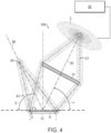
- Figure 4 is a schematic view of a further embodiment of an illumination system 100.
- the beam splitter 4 is omitted.
- the configurable area light source 2 is arranged such that the optical axis 20 of the illumination beam path 21 is tilted at an angle ⁇ with respect to surface 5 of the object 6.
- the light from the area light source 2 is imaged by the illumination lens 12 onto the surface 5 of the object 6.
- the light reflected from the surface 5 of the object 6 propagates along the imaging optical axis 80 of the illumination beam path 81.
- the field of view 13 on the surface 5 of the object 6 is imaged onto the imaging lens pupil (aperture) 83 (imaging lens and camera not shown).
- the imaging optical axis 80 of the imaging beam path 81 is tilted at an angle ⁇ with respect to the surface 5 of the object 6.
- the optical setup of the illumination system 100 is such that the value of an angle ⁇ of the optical axis 20 of the illumination beam path 21 equals the value of an angle ⁇ of the imaging optical axis 80 of the imaging beam path 81.
- the bright field illumination is achieved without the use of the beam splitter. In other words: an inspection tool where the value of the illumination angle ⁇ equals the value of the imaging angle ⁇ .
- Figure 5 is a schematic view of the value degree of the collimation beam opening angle 84 without the use of an illumination lens 12. Instead of the illumination lens 12 a diffuser plate 11 of an area light source (nor shown here) is positioned prior to the beam splitter 4. As a result from the illumination of the object 6 with a wide beam and without an illumination lens 12 one obtains an asymmetric wide beam which is a traditional wide coaxial illumination. Because of the wide beam opening angle 22 (see Figure 3 ) the imaging quality of the object 6 in the camera 8 will not be sensitive to a tilt of surface 5 of object.
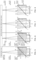
- Figure 6 to Figure 8 show the dependence of the collimation beam opening angle 84 from the spot size (area diameter) of the illumination light.
- Figure 6 is a schematic view of the degree of collimation beam opening angle 84 using a configurable area light source 2 with a huge spot size (huge area diameter) and an illumination lens 12. Due to the huge spot size (huge area diameter) set by the configurable area light source a portion 24 of the collimation beam opening angle 84 is cut off. This makes the beam opening angle 84 asymmetrical towards the edges of the field of view 13. The light, reflected from the surface 5 of the object 6, is not sensitive to a tilt of the beam splitter 4.
- Figure 7 is a schematic view of the degree of collimation beam opening angle 84 using a configurable area light source with an intermediate spot size (reduced spot size compared to figure 6 ). From the illumination lens 12 the light from the configurable area light source is collimated via the beam splitter 4 onto the surface 5 of the object 6. From figure 7 it is clear that with the reduced spot size the collimation beam opening angle 84 becomes narrower. Additionally, the light reflected from the surface 5 of the object 6 is now sensitive to a tilt of the surface 5 object 6.
- Figure 8 is a schematic view of the degree of collimation beam opening angle 84. Compared with the schematic view of figure 7 the spot size is reduced further. The configurable area light source 2 has now a small spot size (small area diameter).
- the result of the narrow beam opening angle is that the set-up of the illumination system is very sensitive to the tilt of the surface 5 of the object 6. Additionally, the light reflected from the surface 5 of the object 6 becomes more collimated compared with the spot sizes (area diameters) shown in figure 6 or 7 .
- FIG 9 is a top view of an embodiment of a configurable area light source 2 not forming part of the claimed invention.
- the area light source 2 is configured by a plurality of light emitting elements 14, which are arranged in a 2-dimensional manner on a carrier 16.
- the light emitting elements 14 are arranged in rows 17 1 , 17 2 ,...,17 N and columns 18 1 , 18 2 ,...,18 N and thereby form a matrix.
- the light emitting elements 14 are light emitting diodes (LEDs).
- the configurable area light source 2 is assigned to a control and drive device 30, or any embedded system which can address the area light source 2 accordingly.
- Figure 9 shows one embodiment not forming part of the claimed invention how the different sizes 19 1 , 19 2 ,...,19 N of the configurable area light source 2 are initialized.
- the light emitting elements 14 are addressed by the control and drive device 30 such that various sizes of the circles of the area light source 2 are addressed. It has to be noted that the addressable form of circles of the configurable area light source 2 should not be considered as a limiting factor.
- Figure 10 is a side view of the embodiment of the configurable area light source 2 of figure 9 which does not form part of the claimed invention.
- the light emitting elements 14 are arranged on the carrier 16.
- the configurable area light source 2 in addition can be provided with a diffuser (not shown) in order to achieve a uniform light distribution (area) of the addressed light emitting elements 14 on the carrier 16.
- the configurable area light source 2 is an area made of concentric geometrical shapes 23.
- the ideal solution would be to use concentric circles 25.
- This embodiment which does not form part of the claimed invention is shown in Figure 11 , wherein the configurable area light source 2 is formed by the light emitting elements 14 already positioned in the shape of the concentric circles 25.
- Figure 12 shows another embodiment of a configurable area light source 2 which does not form part of the claimed invention.
- the easiest solution for the positioning of the light emitting elements 14 would be to use concentric rectangles 26.
- the geometrical shapes 23 are rectangles, which have the drawback that the collimation angles are different for the diagonal direction versus the horizontal/vertical direction of the rectangles.
- Figure 13 shows an embodiment of the present invention of a configurable area light source 2.
- a good compromise compared with the embodiment shown in figure 12 , is to use concentric hexagons 27 as the concentric shapes 23. This may be achieved for example by making a staggered grid of light emitting elements 14 (not shown here).
- the design of the area light source is not limited to concentric geometrical shapes 23 shown in figures 11 to 13 .
- any pattern can be projected by addressing the light emitting elements 14 of the area light source 2. This will result in light beams having the desired pattern and the desired light beam opening angle.
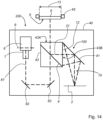
- Figure 14 shows a possible embodiment of the integration of the inventive illumination system 100 into an inspection apparatus 200.
- the inventive illumination system 100 is integrated in an existing housing 40 of the inspection apparatus 200.
- the inventive illumination system 100 provides different light beam opening angles in one coaxial illumination setup.
- the light 10 from the configurable area light source 2 is directed via a mirror 41 to the illumination lens 12 (one possible embodiment of the illumination lens 12 is a Fresnel lens).
- the mirror 41 is necessary for folding illumination beam path 21. This saves space and enables the integration of the illumination system 100 into the inspection apparatus 200.
- the beam splitter 4 of the inventive illumination system 100 is mounted in a holder 43.
- the object 6, to be inspected is held by a carrier 45 so that the surface 5 of the object 6 faces a first side face 43A of the holder 43.
- the mirror 41 is mounted to a second side face 43B of the holder 43 such that illumination light 10 from the configurable area light source 2 is directed via the illumination lens 12 onto the beam splitter 4 and from there onto the surface 5 of the object 6.
- the light reflected from the surface 5 of the object 6 travels along the imaging beam path 81 to the camera 8.
- the imaging lens 7 images a field of view 13 of the surface 5 of the object 6 into the image plane 9 of the camera 8.
- two additional mirrors 82 are provided in the imaging beam path 81, in order to fold the imaging beam path 81 for space reasons.
- FIG 15 shows an additional embodiment which does not form part of the claimed invention of a configurable area light source 2.
- a LCD-screen 50 is positioned after at least one light emitting element 14.
- a single light emitting element 14 is used which provides a homogeneous area lightning of the back of the LCD 50 (see the side view configurable area light source 2 as shown in Figure 16 ).
- the plurality of pixels 51 of the LCD 50 can be addressed individually.
- the LCD 50 comprises a plurality of pixels 51, arranged in a 2-dimensional manner. Accordingly, various illumination patterns can be formed by addressing the pixels 51 individually by a known control device (not shown).
- the pixels 51 of the configurable area light source 2 are addressed in a manner , so that a group of pixels block the light 55 from the light emitting element 14 completely and the other pixels 51 let the light 55 from the light emitting element 14 pass (see figure 16 ). It is evident for a skilled person that the transmittance of the individual pixels 51can be adjusted as well.
Description
- The present invention refers to an illumination system.
- Furthermore, the present invention refers to an inspection tool with an illumination system.
- Additionally, the present invention refers to a method of operating an illumination system.
- Japanese patent application
JP 2013-145123 A - Japanese patent application
JP 2011-106912 A -
WO2010029549 discloses a surface scanning device for inspecting a product surface includes an illumination module and an image acquisition device. -
US7352467 describes a surface plasmon resonance imaging system and method. -
US5949584 discloses an imaging system for viewing indicia on an object to be observed in which the indicia comprises a plurality of either hard and/or soft marks. - A first aspect of the present invention provides a method for inspecting an object as recited in
claim 1. A second aspect of the present invention provides an inspection tool as recited inclaim 2. - Below, the invention and its advantages will be further described with reference to the accompanying figures in which:
-
Fig. 1 is a schematic view of a prior art wide angle coaxial illumination system using a big diffuse light source. -
Fig. 2 is a schematic view of a prior art collimated coaxial illumination system using a point light source. -
Fig. 3 is a schematic view of an inventive concept of a collimated coaxial illumination system. -
Fig. 4 is a schematic view of an inventive concept of a collimated illumination system. -
Fig. 5 is a schematic view of the degree of the collimation beam opening angle of the light from an area light source without the use of an illumination lens. -
Fig. 6 is a schematic view of the degree of the collimation beam opening angle of the light from a configurable area light source, wherein the illumination system provides a huge spot size from the area light source in combination with the illumination lens. -
Fig. 7 is a schematic view of the degree of the collimation beam opening angle of the light from a configurable area light source, wherein the illumination system provides an intermediate spot size from the area light source in combination with the illumination lens. -
Fig. 8 is a schematic view of the degree of the collimation beam opening angle of the light from a configurable area light source wherein the illumination system provides a small spot size from the area light source in combination with the illumination lens. -
Fig. 9 is a top view of an embodiment not forming part of the claimed invention of a configurable area light source. -
Fig. 10 is a side view of the embodiment not forming part of the claimed invention of the configurable area light source ofFig. 9 . -
Fig. 11 shows one embodiment not forming part of the claimed invention of a configurable area light source. -
Fig. 12 shows another embodiment not forming part of the claimed invention of a configurable area light source. -
Fig. 13 shows an embodiment of a configurable area light source embodying the present invention. -
Fig. 14 shows the integration of the inventive illumination system into an inspection tool or apparatus. -
Fig. 15 is a top view of a further embodiment of the configurable area light source, wherein a LCD is used for forming the illumination pattern. -
Fig. 16 is a side view of the embodiment of the configurable area light source ofFig. 15 . - In the figures like reference numerals are used for like elements or elements of like function. Furthermore, for the sake of clarity, only those reference numerals are shown in the figures which are necessary for discussing the respective figure.
-
Figure 1 is a schematic view of a priorart illumination system 100 which is configured as wide anglecoaxial illumination system 100 using a big diffusearea light source 2. The working principle of the wide anglecoaxial illumination system 100 is that the big diffusearea light source 2 projects itslight 3 via abeam splitter 4 towards asurface 5 of anobject 6. Thelight source 2 is arranged in anoptical axis 20 of anillumination beam path 21. Theillumination system 100 is acoaxial illumination system 100, because downstream from thebeam splitter 4 thelight 3 from thelight source 2 has the same approximate direction D as an imagingoptical axis 80 of animaging beam path 81. Acamera 8 is arranged in the imagingoptical axis 80 of theimaging beam path 81. Animaging lens 7 images a portion or field of view of thesurface 5 of theobject 6 onto animage plane 9 of thecamera 8. Thelight 10 reflected from thesurface 5 of theobject 6 travels along the imagingoptical axis 80 of theimaging beam path 81 and, after passing thebeam splitter 4, reaches theimaging lens 7 of thecamera 8. -
Figure 2 is a schematic view of a priorart illumination system 100, which is configured as a collimatedcoaxial illumination system 100 using apoint light source 15. In order to obtain the collimated coaxial illumination, apoint light source 15 is projected by anillumination lens 12 viabeam splitter 4 towardssurface 5 ofobject 6. Thepoint light source 15 is arranged in anoptical axis 20 of anillumination beam path 21. Theillumination system 100 is a collimatedcoaxial illumination system 100, because downstream from thebeam splitter 4 thelight 3 from thepoint light source 15 has the same approximate direction D as an imagingoptical axis 80 of an imaging beam path 81and is focused on theaperture 83 of the imaging lens 7 (provided theobject 6 is a mirror-like device). Thecamera 8 is arranged in the imagingoptical axis 80 of theimaging beam path 81. In case theobject 6 would be a mirror, thepoint light source 15 would be projected and focused exactly on the lens pupil (aperture) 83 (seeFigure 3 ) of theimaging lens 7. This is the case if theimaging lens 7 is a perspective lens. In case theimaging lens 7 is a telecentric lens, thepoint light source 15 would be projected to infinity. - The imaging lens 7 images a portion or field of view of the
surface 5 of theobject 6 onto animage plane 9 of thecamera 8. Thelight 10 reflected from thesurface 5 of theobject 6 travels along the imagingoptical axis 80 of animaging beam path 81 and, after passing thebeam splitter 4, reaches theimaging lens 7 of thecamera 8. -
Figure 3 is a schematic view of an embodiment not forming of the claimed invention of anillumination system 100, which is a collimatedcoaxial illumination system 100. Theinventive illumination system 100 combines the functionality of a wide angle coaxial illumination and a collimated coaxial illumination in onearea light source 2. The configurable arealight source 2 is configured such thatdifferent area diameters - In case of a very small area diameter, like
area diameter 21, theillumination system 100 is comparable to theillumination system 100 offigure 2 using the point light source functionality. The selection of thesmallest area diameter 21 results in very narrow beam of collimated coaxial illumination. - In case the complete area, the largest area diameter 2rr, of the configurable area
light source 2 is selected or initialized, the set-up is comparable to the set-up with the diffuse arealight source 2 offigure 1 wherein the diffuse arealight source 2 is at the location of the pointlight source 15 offigure 2 . The result is a collimated coaxial illumination having a very wide beam coaxial illumination. This illumination is comparable to the light coming from a traditional "wide angle coaxial illumination". According to the invention the light from the configurable arealight source 2 is projected now through theillumination lens 12 onto thebeam splitter 4 and from there onto thesurface 5 of thesample 6. - The area
light source 2 is arranged in theoptical axis 20 of theillumination beam path 21. As mentioned before, the configurable arealight source 2 is configured such that the differentsettable area diameters area diameter smallest diameter 21 and thelargest area diameter 2N allows a variation of the collimationbeam opening angle 22. - In case the configurable area
light source 2 is set such that only theouter area diameters 22 ,..., 2N are used (send out light) a dark spot remains in the center 2C of the configurable arealight source 2. This set-up results in a dark field near coaxial illumination. - The
illumination lens 12 in theillumination beam path 21 illuminates a collimated beam onto a field ofview 13 on thesurface 5 of theobject 6. From thesurface 5 of theobject 6 the field ofview 13 is imaged along the imagingoptical axis 80 ofimaging beam path 81 onto the imaging lens pupil (aperture) 83 of the imaging lens (imaging lens and camera not shown here). -
Figure 4 is a schematic view of a further embodiment of anillumination system 100. Thebeam splitter 4 is omitted. The configurable arealight source 2 is arranged such that theoptical axis 20 of theillumination beam path 21 is tilted at an angle α with respect tosurface 5 of theobject 6. As mentioned above, the light from the arealight source 2 is imaged by theillumination lens 12 onto thesurface 5 of theobject 6. The light reflected from thesurface 5 of theobject 6 propagates along the imagingoptical axis 80 of the illumination beam path 81.The field ofview 13 on thesurface 5 of theobject 6 is imaged onto the imaging lens pupil (aperture) 83 (imaging lens and camera not shown). The imagingoptical axis 80 of theimaging beam path 81 is tilted at an angle β with respect to thesurface 5 of theobject 6. The optical setup of theillumination system 100 is such that the value of an angle α of theoptical axis 20 of theillumination beam path 21 equals the value of an angle β of the imagingoptical axis 80 of theimaging beam path 81. The bright field illumination is achieved without the use of the beam splitter. In other words: an inspection tool where the value of the illumination angle α equals the value of the imaging angle β. -
Figure 5 is a schematic view of the value degree of the collimationbeam opening angle 84 without the use of anillumination lens 12. Instead of the illumination lens 12 adiffuser plate 11 of an area light source (nor shown here) is positioned prior to thebeam splitter 4. As a result from the illumination of theobject 6 with a wide beam and without anillumination lens 12 one obtains an asymmetric wide beam which is a traditional wide coaxial illumination. Because of the wide beam opening angle 22 (seeFigure 3 ) the imaging quality of theobject 6 in thecamera 8 will not be sensitive to a tilt ofsurface 5 of object. -
Figure 6 to Figure 8 show the dependence of the collimationbeam opening angle 84 from the spot size (area diameter) of the illumination light.Figure 6 is a schematic view of the degree of collimationbeam opening angle 84 using a configurable arealight source 2 with a huge spot size (huge area diameter) and anillumination lens 12. Due to the huge spot size (huge area diameter) set by the configurable area light source aportion 24 of the collimationbeam opening angle 84 is cut off. This makes thebeam opening angle 84 asymmetrical towards the edges of the field ofview 13. The light, reflected from thesurface 5 of theobject 6, is not sensitive to a tilt of thebeam splitter 4.Figure 7 is a schematic view of the degree of collimationbeam opening angle 84 using a configurable area light source with an intermediate spot size (reduced spot size compared tofigure 6 ). From theillumination lens 12 the light from the configurable area light source is collimated via thebeam splitter 4 onto thesurface 5 of theobject 6. Fromfigure 7 it is clear that with the reduced spot size the collimationbeam opening angle 84 becomes narrower. Additionally, the light reflected from thesurface 5 of theobject 6 is now sensitive to a tilt of thesurface 5object 6.Figure 8 is a schematic view of the degree of collimationbeam opening angle 84. Compared with the schematic view offigure 7 the spot size is reduced further. The configurable arealight source 2 has now a small spot size (small area diameter). The result of the narrow beam opening angle is that the set-up of the illumination system is very sensitive to the tilt of thesurface 5 of theobject 6. Additionally, the light reflected from thesurface 5 of theobject 6 becomes more collimated compared with the spot sizes (area diameters) shown infigure 6 or 7 . -
Figure 9 is a top view of an embodiment of a configurable arealight source 2 not forming part of the claimed invention. In the embodiment shown here, the arealight source 2 is configured by a plurality oflight emitting elements 14, which are arranged in a 2-dimensional manner on acarrier 16. Here thelight emitting elements 14 are arranged in rows 171, 172,...,17N and columns 181, 182,...,18N and thereby form a matrix. According to one possible embodiment, thelight emitting elements 14 are light emitting diodes (LEDs). As shown infigures 3 and4 , the configurable arealight source 2 is assigned to a control and drivedevice 30, or any embedded system which can address the arealight source 2 accordingly. With the control and drivedevice 30 it is possible to address the individuallight emitting elements 14 and generate different light emitting shapes and/or sizes of the configurable arealight source 2.Figure 9 shows one embodiment not forming part of the claimed invention how thedifferent sizes light source 2 are initialized. Thelight emitting elements 14 are addressed by the control and drivedevice 30 such that various sizes of the circles of the arealight source 2 are addressed. It has to be noted that the addressable form of circles of the configurable arealight source 2 should not be considered as a limiting factor. -
Figure 10 is a side view of the embodiment of the configurable arealight source 2 offigure 9 which does not form part of the claimed invention. Thelight emitting elements 14 are arranged on thecarrier 16. The configurable arealight source 2 in addition can be provided with a diffuser (not shown) in order to achieve a uniform light distribution (area) of the addressedlight emitting elements 14 on thecarrier 16. - The configurable area
light source 2 is an area made of concentric geometrical shapes 23. The ideal solution would be to useconcentric circles 25. This embodiment which does not form part of the claimed invention is shown inFigure 11 , wherein the configurable arealight source 2 is formed by thelight emitting elements 14 already positioned in the shape of theconcentric circles 25. -
Figure 12 shows another embodiment of a configurable arealight source 2 which does not form part of the claimed invention. The easiest solution for the positioning of thelight emitting elements 14 would be to useconcentric rectangles 26. Thegeometrical shapes 23 are rectangles, which have the drawback that the collimation angles are different for the diagonal direction versus the horizontal/vertical direction of the rectangles. -
Figure 13 shows an embodiment of the present invention of a configurable arealight source 2. A good compromise, compared with the embodiment shown infigure 12 , is to useconcentric hexagons 27 as the concentric shapes 23. This may be achieved for example by making a staggered grid of light emitting elements 14 (not shown here). - However, the design of the area light source is not limited to concentric
geometrical shapes 23 shown infigures 11 to 13 . In fact any pattern can be projected by addressing thelight emitting elements 14 of the arealight source 2. This will result in light beams having the desired pattern and the desired light beam opening angle. -
Figure 14 shows a possible embodiment of the integration of theinventive illumination system 100 into aninspection apparatus 200. Theinventive illumination system 100 is integrated in an existinghousing 40 of theinspection apparatus 200. Theinventive illumination system 100 provides different light beam opening angles in one coaxial illumination setup. The light 10 from the configurable arealight source 2 is directed via amirror 41 to the illumination lens 12 (one possible embodiment of theillumination lens 12 is a Fresnel lens). Themirror 41 is necessary for foldingillumination beam path 21. This saves space and enables the integration of theillumination system 100 into theinspection apparatus 200. - The
beam splitter 4 of theinventive illumination system 100 is mounted in aholder 43. Theobject 6, to be inspected, is held by acarrier 45 so that thesurface 5 of theobject 6 faces afirst side face 43A of theholder 43. Themirror 41 is mounted to asecond side face 43B of theholder 43 such that illumination light 10 from the configurable arealight source 2 is directed via theillumination lens 12 onto thebeam splitter 4 and from there onto thesurface 5 of theobject 6. - The light reflected from the
surface 5 of theobject 6 travels along theimaging beam path 81 to thecamera 8. Theimaging lens 7 images a field ofview 13 of thesurface 5 of theobject 6 into theimage plane 9 of thecamera 8. In the embodiment shown here, twoadditional mirrors 82 are provided in theimaging beam path 81, in order to fold theimaging beam path 81 for space reasons. With theinventive inspection apparatus 200 it is possible to provide different light beam opening angles in one coaxial illumination setup. -
Figure 15 shows an additional embodiment which does not form part of the claimed invention of a configurable arealight source 2. A LCD-screen 50 is positioned after at least onelight emitting element 14. In the embodiment shown here, a singlelight emitting element 14 is used which provides a homogeneous area lightning of the back of the LCD 50 (see the side view configurable arealight source 2 as shown inFigure 16 ). The plurality ofpixels 51 of theLCD 50 can be addressed individually. TheLCD 50 comprises a plurality ofpixels 51, arranged in a 2-dimensional manner. Accordingly, various illumination patterns can be formed by addressing thepixels 51 individually by a known control device (not shown). Thepixels 51 of the configurable area light source 2 (seeFigure 15 ) are addressed in a manner , so that a group of pixels block the light 55 from thelight emitting element 14 completely and theother pixels 51 let the light 55 from thelight emitting element 14 pass (seefigure 16 ). It is evident for a skilled person that the transmittance of the individual pixels 51can be adjusted as well. -
- 2
- area light source; configurable area light source
- 21, 22 ,..., 2N
- area diameter
- 2C
- center of area light source
- 3
- light
- 4
- beam splitter
- 5
- surface
- 6
- object
- 7
- imaging lens
- 8
- camera
- 9
- image plane
- 10
- light
- 11
- diffuser plate
- 12
- illumination lens
- 13
- field of view
- 14
- light emitting elements
- 15
- point light source
- 16
- carrier
- 171, 172,...,17N
- row
- 181, 182,...,18N
- column
- 191, 192,...,19N
- size
- 20
- illumination optical axis
- 21
- illumination beam path
- 22
- collimated beam opening angle (before illumination lens)
- 23
- concentric geometrical shape
- 24
- portion
- 25
- concentric circles
- 26
- concentric rectangles
- 27
- concentric hexagons
- 30
- control and drive device
- 40
- housing
- 41
- mirror
- 43
- holder
- 43A
- first side face
- 43B
- second side face
- 50
- LCD
- 51
- pixels of LCD
- 55
- light
- 80
- imaging optical axis
- 81
- imaging beam path
- 82
- mirror
- 83
- imaging lens pupil, aperture
- 84
- collimated beam opening angle (after imaging lens)
- 100
- illumination system
- 200
- inspection apparatus
- D
- direction
- α
- angle
- β
- angle
Claims (4)
- A method for inspecting an object (6), comprising:a. directing illumination light, the illumination light defining a light beam opening angle, from a configurable area light source (2) onto a beam splitter (4) via an illumination lens (12) along an illumination beam path (21) onto a surface (5) of an object (6);b. directing reflected light from the surface (5) of the object (6) along an imaging beam path (81);c. imaging the reflected light from the surface (5) of the object (6) with an imaging lens (7) onto an image plane (9) of a camera (8);d. changing the diameter of the illumination light and thereby changing the opening angle of the light beam;e. repeating the steps a - d; andgenerating a field of view on the surface (5) of the object (6) in real time images with different beam opening angles and collimation angles, respectively, wherein the configurable area light source (2) is a 2-dimensional arrangement of a plurality of light emitting elements (14); wherein the plurality of light emitting elements (14) includes a plurality of light emitting diodes; wherein the 2-dimensional arrangement of the plurality of light emitting elements (14) is defined by an arrangement of the plurality of light emitting elements (14) in a plurality of concentric geometrical shapes (23); wherein a control and drive device (30) is assigned to the configurable area light source (2) so that the plurality of concentric and addressable geometrical shapes are generated in order to obtain different beam diameters, wherein the plurality of concentric geometrical shapes (23) include a plurality of concentric hexagons (27).
- An inspection tool (200) configured to implement the method of claim 1, comprising:a camera (8), arranged in an imaging optical axis (80) of an imaging beam path (81);an imaging lens (83) positioned in the imaging beam path (81) for imaging at least a portion of a surface (5) of an object (6) into an image plane (9) of the camera (8);an illumination system (100) with a configurable area light source (2), wherein the configurable area light source (2) is arranged in an illumination optical axis (20) of an illumination beam path (21) and the configurable area light source (2) is configured such that different beam diameters are settable;at least one illumination lens (12) positioned in the illumination beam path (21) for directing a collimated beam onto a field of view on the surface (5) of the object (6), wherein a value of an angle of incidence of the illumination optical axis (20) of the illumination beam path (21) equals a value of an angle of reflectance of an imaging optical axis of the imaging beam path;a beam splitter (4) positioned in the illumination path after the at least one illumination lens (12), wherein the beam splitter (4) directs collimated illumination light from the configurable area light source (2) along a redirected illumination optical axis of the illumination beam path onto the surface (5) of the object (6), and wherein the imaging optical axis of the imaging beam path is coaxial with the redirected illumination optical axis of the illumination beam path; andwherein the settable different beam diameters enable a variation of a collimated beam opening angle (22);wherein the configurable area light source (2) is a 2-dimensional arrangement of a plurality of light emitting elements (14); wherein the plurality of light emitting elements (14) includes a plurality of light emitting diodes; wherein the 2-dimensional arrangement of the plurality of light emitting elements (14) is defined by an arrangement of the plurality of light emitting elements (14) in a plurality of concentric geometrical shapes (23);a control and drive device (30) assigned to the configurable area light source (2) so that a plurality of concentric geometrical shapes (23) of illumination are generated in order to obtain different beam diameters, wherein the plurality of concentric geometrical shapes (23) include a plurality of concentric hexagons (27).
- The inspection tool as claimed in claim 2, wherein the imaging beam path (81) is folded at least one time for directing light from the field of view on the surface (5) of the object onto the image plane (9) of the camera (8); or
wherein the illumination beam path (81) is folded at least one time for directing light from the configurable area light source (2) onto the surface (5) of the object (6). - The inspection tool as claimed in any preceding claim, wherein the object (6) is a mirror, the imaging beam path (81) is directed exactly onto the lens pupil of the imaging lens (83).
Applications Claiming Priority (2)
| Application Number | Priority Date | Filing Date | Title |
|---|---|---|---|
| US201462073393P | 2014-10-31 | 2014-10-31 | |
| PCT/US2015/058486 WO2016070133A1 (en) | 2014-10-31 | 2015-10-30 | Illumination system, inspection tool with illumination system, and method of operating an illumination system |
Publications (3)
| Publication Number | Publication Date |
|---|---|
| EP3140638A1 EP3140638A1 (en) | 2017-03-15 |
| EP3140638A4 EP3140638A4 (en) | 2018-01-24 |
| EP3140638B1 true EP3140638B1 (en) | 2024-02-14 |
Family
ID=55858432
Family Applications (1)
| Application Number | Title | Priority Date | Filing Date |
|---|---|---|---|
| EP15853870.2A Active EP3140638B1 (en) | 2014-10-31 | 2015-10-30 | Illumination system, inspection tool with illumination system, and method of operating an illumination system |
Country Status (9)
| Country | Link |
|---|---|
| EP (1) | EP3140638B1 (en) |
| JP (2) | JP2017533437A (en) |
| KR (1) | KR102272438B1 (en) |
| CN (2) | CN106796181A (en) |
| MY (1) | MY188346A (en) |
| PH (1) | PH12017500736A1 (en) |
| SG (1) | SG11201702728UA (en) |
| TW (1) | TWI697662B (en) |
| WO (1) | WO2016070133A1 (en) |
Families Citing this family (5)
| Publication number | Priority date | Publication date | Assignee | Title |
|---|---|---|---|---|
| KR101795322B1 (en) | 2016-12-30 | 2017-11-08 | 허철 | Dual imaging telecentric optics for inspection of OLED |
| EP3803494A1 (en) * | 2018-06-04 | 2021-04-14 | JENOPTIK Optical Systems GmbH | Microscope and method for capturing a microscopic image and use of a planar reflector |
| WO2020148749A1 (en) * | 2019-01-14 | 2020-07-23 | Orbotech Ltd. | Multiplexed image acquisition device for optical system |
| US10816464B2 (en) * | 2019-01-23 | 2020-10-27 | Applied Materials, Inc. | Imaging reflectometer |
| JP7392582B2 (en) * | 2020-06-12 | 2023-12-06 | オムロン株式会社 | Inspection system and method |
Family Cites Families (15)
| Publication number | Priority date | Publication date | Assignee | Title |
|---|---|---|---|---|
| US5949584A (en) * | 1997-05-13 | 1999-09-07 | Northeast Robotics Llc | Wafer |
| JP3472750B2 (en) * | 2000-04-10 | 2003-12-02 | シーシーエス株式会社 | Surface inspection equipment |
| US20040042001A1 (en) * | 2002-04-18 | 2004-03-04 | Kla-Tencor Technologies Corporation | Simultaneous multi-spot inspection and imaging |
| US6870949B2 (en) * | 2003-02-26 | 2005-03-22 | Electro Scientific Industries | Coaxial narrow angle dark field lighting |
| US7352467B2 (en) * | 2003-10-24 | 2008-04-01 | University Of Washington | Surface plasmon resonance imaging system and method |
| CN100433245C (en) * | 2004-03-11 | 2008-11-12 | 株式会社液晶先端技术开发中心 | Laser crystallization apparatus and laser crystallization method |
| US7738092B1 (en) * | 2008-01-08 | 2010-06-15 | Kla-Tencor Corporation | System and method for reducing speckle noise in die-to-die inspection systems |
| US7990531B2 (en) * | 2008-06-05 | 2011-08-02 | Coopervision International Holding Company, Lp | Multi-imaging automated inspection methods and systems for wet ophthalmic lenses |
| US8502968B2 (en) * | 2008-09-12 | 2013-08-06 | Ceramicam Ltd. | Surface scanning device |
| JP2012083211A (en) * | 2010-10-12 | 2012-04-26 | Canon Inc | Surface state inspection device, surface state inspection method and program |
| JP5027946B1 (en) * | 2011-12-28 | 2012-09-19 | 新明和工業株式会社 | Inspection system |
| JP2013145123A (en) * | 2012-01-13 | 2013-07-25 | Seiwa Optical Co Ltd | Optical system with wide-angle reflection coaxial illumination |
| US9128064B2 (en) * | 2012-05-29 | 2015-09-08 | Kla-Tencor Corporation | Super resolution inspection system |
| JP6205780B2 (en) * | 2013-03-27 | 2017-10-04 | 凸版印刷株式会社 | Illumination device and inspection device |
| US9255887B2 (en) * | 2013-06-19 | 2016-02-09 | Kla-Tencor Corporation | 2D programmable aperture mechanism |
-
2015
- 2015-10-30 EP EP15853870.2A patent/EP3140638B1/en active Active
- 2015-10-30 WO PCT/US2015/058486 patent/WO2016070133A1/en active Application Filing
- 2015-10-30 CN CN201580055825.6A patent/CN106796181A/en active Pending
- 2015-10-30 JP JP2017523513A patent/JP2017533437A/en active Pending
- 2015-10-30 TW TW104135916A patent/TWI697662B/en active
- 2015-10-30 SG SG11201702728UA patent/SG11201702728UA/en unknown
- 2015-10-30 KR KR1020177014639A patent/KR102272438B1/en active IP Right Grant
- 2015-10-30 CN CN202210561988.3A patent/CN114813758A/en active Pending
- 2015-10-30 MY MYPI2016002118A patent/MY188346A/en unknown
-
2017
- 2017-04-20 PH PH12017500736A patent/PH12017500736A1/en unknown
-
2021
- 2021-03-30 JP JP2021057066A patent/JP7193571B2/en active Active
Also Published As
| Publication number | Publication date |
|---|---|
| CN114813758A (en) | 2022-07-29 |
| PH12017500736A1 (en) | 2017-10-09 |
| CN106796181A (en) | 2017-05-31 |
| JP7193571B2 (en) | 2022-12-20 |
| KR102272438B1 (en) | 2021-07-02 |
| TWI697662B (en) | 2020-07-01 |
| MY188346A (en) | 2021-12-01 |
| WO2016070133A1 (en) | 2016-05-06 |
| EP3140638A4 (en) | 2018-01-24 |
| TW201627656A (en) | 2016-08-01 |
| EP3140638A1 (en) | 2017-03-15 |
| JP2021101194A (en) | 2021-07-08 |
| SG11201702728UA (en) | 2017-05-30 |
| KR20170080631A (en) | 2017-07-10 |
| JP2017533437A (en) | 2017-11-09 |
Similar Documents
| Publication | Publication Date | Title |
|---|---|---|
| US10379057B2 (en) | Illumination system, inspection tool with illumination system, and method of operating an illumination system | |
| JP7193571B2 (en) | Illumination system, inspection tool having illumination system, and method of operating illumination system | |
| EP1581781B1 (en) | Method and apparatus for simultaneous 2-d and topographical inspection | |
| US8928892B2 (en) | Wavefront analysis inspection apparatus and method | |
| US11531193B2 (en) | Optical arrangement, multi-spot scanning microscope and method for operating a microscope | |
| TWI557434B (en) | Lighting system | |
| KR102373287B1 (en) | Telecentric bright field and annular dark field seamlessly fused illumination | |
| KR102226444B1 (en) | Adaptive diffuse illumination systems and methods | |
| US20180156414A1 (en) | Vehicle lighting apparatus | |
| JP2016024195A5 (en) | ||
| JP2017533437A5 (en) | ||
| TWI393873B (en) | Device and method for controlling an angular coverage of a light beam | |
| JPH0771917A (en) | Lead inspecting device of semiconductor device | |
| JP6513980B2 (en) | Imaging apparatus and imaging method | |
| JP2021085815A (en) | Light irradiation device, inspection system, and light irradiation method | |
| US20180080880A1 (en) | Optical scattering measurement method and apparatus using micro lens matrix | |
| JP2013083726A (en) | Magnifying observation device | |
| JP2008046247A (en) | Microscope apparatus | |
| JP2018066848A (en) | Sheet illumination microscope |
Legal Events
| Date | Code | Title | Description |
|---|---|---|---|
| STAA | Information on the status of an ep patent application or granted ep patent |
Free format text: STATUS: THE INTERNATIONAL PUBLICATION HAS BEEN MADE |
|
| PUAI | Public reference made under article 153(3) epc to a published international application that has entered the european phase |
Free format text: ORIGINAL CODE: 0009012 |
|
| STAA | Information on the status of an ep patent application or granted ep patent |
Free format text: STATUS: REQUEST FOR EXAMINATION WAS MADE |
|
| 17P | Request for examination filed |
Effective date: 20161208 |
|
| AK | Designated contracting states |
Kind code of ref document: A1 Designated state(s): AL AT BE BG CH CY CZ DE DK EE ES FI FR GB GR HR HU IE IS IT LI LT LU LV MC MK MT NL NO PL PT RO RS SE SI SK SM TR |
|
| AX | Request for extension of the european patent |
Extension state: BA ME |
|
| A4 | Supplementary search report drawn up and despatched |
Effective date: 20171221 |
|
| RIC1 | Information provided on ipc code assigned before grant |
Ipc: G02B 26/00 20060101ALI20171215BHEP Ipc: G01N 21/84 20060101AFI20171215BHEP |
|
| DAV | Request for validation of the european patent (deleted) | ||
| DAX | Request for extension of the european patent (deleted) | ||
| STAA | Information on the status of an ep patent application or granted ep patent |
Free format text: STATUS: EXAMINATION IS IN PROGRESS |
|
| 17Q | First examination report despatched |
Effective date: 20180913 |
|
| STAA | Information on the status of an ep patent application or granted ep patent |
Free format text: STATUS: EXAMINATION IS IN PROGRESS |
|
| STAA | Information on the status of an ep patent application or granted ep patent |
Free format text: STATUS: EXAMINATION IS IN PROGRESS |
|
| P01 | Opt-out of the competence of the unified patent court (upc) registered |
Effective date: 20230526 |
|
| GRAP | Despatch of communication of intention to grant a patent |
Free format text: ORIGINAL CODE: EPIDOSNIGR1 |
|
| STAA | Information on the status of an ep patent application or granted ep patent |
Free format text: STATUS: GRANT OF PATENT IS INTENDED |
|
| INTG | Intention to grant announced |
Effective date: 20230913 |
|
| GRAS | Grant fee paid |
Free format text: ORIGINAL CODE: EPIDOSNIGR3 |
|
| GRAA | (expected) grant |
Free format text: ORIGINAL CODE: 0009210 |
|
| STAA | Information on the status of an ep patent application or granted ep patent |
Free format text: STATUS: THE PATENT HAS BEEN GRANTED |
|
| AK | Designated contracting states |
Kind code of ref document: B1 Designated state(s): AL AT BE BG CH CY CZ DE DK EE ES FI FR GB GR HR HU IE IS IT LI LT LU LV MC MK MT NL NO PL PT RO RS SE SI SK SM TR |
|
| REG | Reference to a national code |
Ref country code: GB Ref legal event code: FG4D |
|
| RIN1 | Information on inventor provided before grant (corrected) |
Inventor name: GOORMAN, KOEN Inventor name: BEGOC, PAULINE Inventor name: DE GREEVE, JOHAN Inventor name: CAUWENBERGHS, FILIP |
|
| REG | Reference to a national code |
Ref country code: CH Ref legal event code: EP |
|
| REG | Reference to a national code |
Ref country code: DE Ref legal event code: R096 Ref document number: 602015087564 Country of ref document: DE |
|
| REG | Reference to a national code |
Ref country code: IE Ref legal event code: FG4D |
|
| REG | Reference to a national code |
Ref country code: NL Ref legal event code: FP |