EP3139708B1 - Triac-steuerungssysteme - Google Patents
Triac-steuerungssysteme Download PDFInfo
- Publication number
- EP3139708B1 EP3139708B1 EP16185910.3A EP16185910A EP3139708B1 EP 3139708 B1 EP3139708 B1 EP 3139708B1 EP 16185910 A EP16185910 A EP 16185910A EP 3139708 B1 EP3139708 B1 EP 3139708B1
- Authority
- EP
- European Patent Office
- Prior art keywords
- triac
- controller
- unit
- power supply
- rectifier
- Prior art date
- Legal status (The legal status is an assumption and is not a legal conclusion. Google has not performed a legal analysis and makes no representation as to the accuracy of the status listed.)
- Active
Links
- 239000003990 capacitor Substances 0.000 claims description 20
- 230000001960 triggered effect Effects 0.000 claims description 7
- 238000000034 method Methods 0.000 description 7
- 230000004224 protection Effects 0.000 description 5
- 230000008901 benefit Effects 0.000 description 3
- 230000002457 bidirectional effect Effects 0.000 description 3
- 230000001052 transient effect Effects 0.000 description 3
- 230000033228 biological regulation Effects 0.000 description 2
- 230000001681 protective effect Effects 0.000 description 2
- 238000005057 refrigeration Methods 0.000 description 2
- 230000000630 rising effect Effects 0.000 description 2
- 238000004804 winding Methods 0.000 description 2
- 238000009825 accumulation Methods 0.000 description 1
- 230000009286 beneficial effect Effects 0.000 description 1
- 230000002146 bilateral effect Effects 0.000 description 1
- 238000010276 construction Methods 0.000 description 1
- 238000001514 detection method Methods 0.000 description 1
- 230000005611 electricity Effects 0.000 description 1
- 238000004146 energy storage Methods 0.000 description 1
- 238000010438 heat treatment Methods 0.000 description 1
- 230000006698 induction Effects 0.000 description 1
- 230000009979 protective mechanism Effects 0.000 description 1
- 230000035945 sensitivity Effects 0.000 description 1
- 239000007787 solid Substances 0.000 description 1
- 230000001360 synchronised effect Effects 0.000 description 1
Images


Classifications
-
- H—ELECTRICITY
- H05—ELECTRIC TECHNIQUES NOT OTHERWISE PROVIDED FOR
- H05B—ELECTRIC HEATING; ELECTRIC LIGHT SOURCES NOT OTHERWISE PROVIDED FOR; CIRCUIT ARRANGEMENTS FOR ELECTRIC LIGHT SOURCES, IN GENERAL
- H05B39/00—Circuit arrangements or apparatus for operating incandescent light sources
- H05B39/04—Controlling
- H05B39/08—Controlling by shifting phase of trigger voltage applied to gas-filled controlling tubes also in controlled semiconductor devices
-
- H—ELECTRICITY
- H02—GENERATION; CONVERSION OR DISTRIBUTION OF ELECTRIC POWER
- H02M—APPARATUS FOR CONVERSION BETWEEN AC AND AC, BETWEEN AC AND DC, OR BETWEEN DC AND DC, AND FOR USE WITH MAINS OR SIMILAR POWER SUPPLY SYSTEMS; CONVERSION OF DC OR AC INPUT POWER INTO SURGE OUTPUT POWER; CONTROL OR REGULATION THEREOF
- H02M1/00—Details of apparatus for conversion
- H02M1/08—Circuits specially adapted for the generation of control voltages for semiconductor devices incorporated in static converters
- H02M1/081—Circuits specially adapted for the generation of control voltages for semiconductor devices incorporated in static converters wherein the phase of the control voltage is adjustable with reference to the AC source
-
- H—ELECTRICITY
- H02—GENERATION; CONVERSION OR DISTRIBUTION OF ELECTRIC POWER
- H02M—APPARATUS FOR CONVERSION BETWEEN AC AND AC, BETWEEN AC AND DC, OR BETWEEN DC AND DC, AND FOR USE WITH MAINS OR SIMILAR POWER SUPPLY SYSTEMS; CONVERSION OF DC OR AC INPUT POWER INTO SURGE OUTPUT POWER; CONTROL OR REGULATION THEREOF
- H02M5/00—Conversion of ac power input into ac power output, e.g. for change of voltage, for change of frequency, for change of number of phases
- H02M5/02—Conversion of ac power input into ac power output, e.g. for change of voltage, for change of frequency, for change of number of phases without intermediate conversion into dc
- H02M5/04—Conversion of ac power input into ac power output, e.g. for change of voltage, for change of frequency, for change of number of phases without intermediate conversion into dc by static converters
- H02M5/22—Conversion of ac power input into ac power output, e.g. for change of voltage, for change of frequency, for change of number of phases without intermediate conversion into dc by static converters using discharge tubes with control electrode or semiconductor devices with control electrode
- H02M5/25—Conversion of ac power input into ac power output, e.g. for change of voltage, for change of frequency, for change of number of phases without intermediate conversion into dc by static converters using discharge tubes with control electrode or semiconductor devices with control electrode using devices of a thyratron or thyristor type requiring extinguishing means
- H02M5/257—Conversion of ac power input into ac power output, e.g. for change of voltage, for change of frequency, for change of number of phases without intermediate conversion into dc by static converters using discharge tubes with control electrode or semiconductor devices with control electrode using devices of a thyratron or thyristor type requiring extinguishing means using semiconductor devices only
- H02M5/2573—Conversion of ac power input into ac power output, e.g. for change of voltage, for change of frequency, for change of number of phases without intermediate conversion into dc by static converters using discharge tubes with control electrode or semiconductor devices with control electrode using devices of a thyratron or thyristor type requiring extinguishing means using semiconductor devices only with control circuit
-
- H—ELECTRICITY
- H02—GENERATION; CONVERSION OR DISTRIBUTION OF ELECTRIC POWER
- H02P—CONTROL OR REGULATION OF ELECTRIC MOTORS, ELECTRIC GENERATORS OR DYNAMO-ELECTRIC CONVERTERS; CONTROLLING TRANSFORMERS, REACTORS OR CHOKE COILS
- H02P27/00—Arrangements or methods for the control of AC motors characterised by the kind of supply voltage
- H02P27/02—Arrangements or methods for the control of AC motors characterised by the kind of supply voltage using supply voltage with constant frequency and variable amplitude
-
- H—ELECTRICITY
- H03—ELECTRONIC CIRCUITRY
- H03K—PULSE TECHNIQUE
- H03K17/00—Electronic switching or gating, i.e. not by contact-making and –breaking
- H03K17/51—Electronic switching or gating, i.e. not by contact-making and –breaking characterised by the components used
- H03K17/56—Electronic switching or gating, i.e. not by contact-making and –breaking characterised by the components used by the use, as active elements, of semiconductor devices
- H03K17/72—Electronic switching or gating, i.e. not by contact-making and –breaking characterised by the components used by the use, as active elements, of semiconductor devices having more than two PN junctions; having more than three electrodes; having more than one electrode connected to the same conductivity region
- H03K17/725—Electronic switching or gating, i.e. not by contact-making and –breaking characterised by the components used by the use, as active elements, of semiconductor devices having more than two PN junctions; having more than three electrodes; having more than one electrode connected to the same conductivity region for ac voltages or currents
-
- H—ELECTRICITY
- H05—ELECTRIC TECHNIQUES NOT OTHERWISE PROVIDED FOR
- H05B—ELECTRIC HEATING; ELECTRIC LIGHT SOURCES NOT OTHERWISE PROVIDED FOR; CIRCUIT ARRANGEMENTS FOR ELECTRIC LIGHT SOURCES, IN GENERAL
- H05B1/00—Details of electric heating devices
- H05B1/02—Automatic switching arrangements specially adapted to apparatus ; Control of heating devices
- H05B1/0227—Applications
-
- H—ELECTRICITY
- H05—ELECTRIC TECHNIQUES NOT OTHERWISE PROVIDED FOR
- H05B—ELECTRIC HEATING; ELECTRIC LIGHT SOURCES NOT OTHERWISE PROVIDED FOR; CIRCUIT ARRANGEMENTS FOR ELECTRIC LIGHT SOURCES, IN GENERAL
- H05B47/00—Circuit arrangements for operating light sources in general, i.e. where the type of light source is not relevant
- H05B47/10—Controlling the light source
-
- H—ELECTRICITY
- H02—GENERATION; CONVERSION OR DISTRIBUTION OF ELECTRIC POWER
- H02M—APPARATUS FOR CONVERSION BETWEEN AC AND AC, BETWEEN AC AND DC, OR BETWEEN DC AND DC, AND FOR USE WITH MAINS OR SIMILAR POWER SUPPLY SYSTEMS; CONVERSION OF DC OR AC INPUT POWER INTO SURGE OUTPUT POWER; CONTROL OR REGULATION THEREOF
- H02M1/00—Details of apparatus for conversion
- H02M1/0003—Details of control, feedback or regulation circuits
- H02M1/0006—Arrangements for supplying an adequate voltage to the control circuit of converters
-
- H—ELECTRICITY
- H02—GENERATION; CONVERSION OR DISTRIBUTION OF ELECTRIC POWER
- H02M—APPARATUS FOR CONVERSION BETWEEN AC AND AC, BETWEEN AC AND DC, OR BETWEEN DC AND DC, AND FOR USE WITH MAINS OR SIMILAR POWER SUPPLY SYSTEMS; CONVERSION OF DC OR AC INPUT POWER INTO SURGE OUTPUT POWER; CONTROL OR REGULATION THEREOF
- H02M5/00—Conversion of ac power input into ac power output, e.g. for change of voltage, for change of frequency, for change of number of phases
- H02M5/02—Conversion of ac power input into ac power output, e.g. for change of voltage, for change of frequency, for change of number of phases without intermediate conversion into dc
- H02M5/04—Conversion of ac power input into ac power output, e.g. for change of voltage, for change of frequency, for change of number of phases without intermediate conversion into dc by static converters
- H02M5/22—Conversion of ac power input into ac power output, e.g. for change of voltage, for change of frequency, for change of number of phases without intermediate conversion into dc by static converters using discharge tubes with control electrode or semiconductor devices with control electrode
- H02M5/275—Conversion of ac power input into ac power output, e.g. for change of voltage, for change of frequency, for change of number of phases without intermediate conversion into dc by static converters using discharge tubes with control electrode or semiconductor devices with control electrode using devices of a triode or transistor type requiring continuous application of a control signal
- H02M5/293—Conversion of ac power input into ac power output, e.g. for change of voltage, for change of frequency, for change of number of phases without intermediate conversion into dc by static converters using discharge tubes with control electrode or semiconductor devices with control electrode using devices of a triode or transistor type requiring continuous application of a control signal using semiconductor devices only
- H02M5/2932—Conversion of ac power input into ac power output, e.g. for change of voltage, for change of frequency, for change of number of phases without intermediate conversion into dc by static converters using discharge tubes with control electrode or semiconductor devices with control electrode using devices of a triode or transistor type requiring continuous application of a control signal using semiconductor devices only with automatic control of output voltage, current or power
-
- H—ELECTRICITY
- H03—ELECTRONIC CIRCUITRY
- H03K—PULSE TECHNIQUE
- H03K2217/00—Indexing scheme related to electronic switching or gating, i.e. not by contact-making or -breaking covered by H03K17/00
- H03K2217/0036—Means reducing energy consumption
-
- H—ELECTRICITY
- H03—ELECTRONIC CIRCUITRY
- H03K—PULSE TECHNIQUE
- H03K2217/00—Indexing scheme related to electronic switching or gating, i.e. not by contact-making or -breaking covered by H03K17/00
- H03K2217/0081—Power supply means, e.g. to the switch driver
Definitions
- the present invention relates to triac power control systems.
- Triacs (formally called bidirectional triode thyristors or bilateral triode thyristors) are used extensively in AC power control systems, and are often controlled by digital circuits, including microcontrollers. Because of their latching characteristic, triacs can be turned on by application of a short current pulse to their gate; when operated from digital circuits, the pulse is usually negative because this polarity is compatible with triac conduction in both polarities of the AC supply.
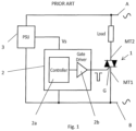
- Fig. 1 shows a prior art AC power control system, which controls the voltage delivered to a load.
- the load is arranged in series with a triac 1 having power terminals labelled MT1 and MT2, and an AC voltage is applied to the combination of the load and triac 1 between terminals A and B.
- the triac is controlled by a control signal generated by a control unit 2 having a controller 2a (typically a microcontrol unit, MCU) for generating a pulse, and a driver circuit 2b used to amplify the current pulse and apply it to a gate (G) of the triac 1.
- a controller 2a typically a microcontrol unit, MCU
- Fig. 2(a) shows, in the top line, the waveform of the AC voltage between terminals A and B.
- the second line is the signal generated by the control unit 2.
- the third line is the voltage across the triac 2
- the fourth (lowest) line is the voltage across the load.
- the controller 2a and drive circuit 2b are powered by a separate low voltage power source unit 3 which is in turn powered by the AC power signal, so the 0V connection of the MCU 2 can be conveniently connected to one of the power terminals of the triac 1.
- Fig. 2 A version with negative polarity is shown in Fig. 2 .
- the controller 2a By using low power circuits in the controller 2a and minimising the duration of the current pulse, the power requirements can be made low - reducing cost and consumption of the power supply circuit. Furthermore, this arrangement is advantageous for some applications where the controller 2a must also connect to other circuits that share a signal reference with the power terminal (MT1) of the triac.
- the power supply unit 3 increases the cost of the power control system and reduces its reliability. Since the power supply 3 is connected directly to the mains supply voltage, it is exposed to high voltages - both nominal and surge (often related to lightning strikes on the electricity supply network). Its components can be highly stressed during surges, and this is a major cause of failure of such products in use. Though the power requirements of the controller are low, the power supply circuits need to be robust against such voltages and this adds to the cost, complexity and size of the power supply 3.
- Fig. 2(b) shows an application which provides a fixed on-time delay T.
- the upper line of Fig. 2(b) shows an AC power signal applied between points A and B, while the lower line of Fig. 2(b) shows the power which the control circuit applies across a load.
- the power applied to the load is zero except during a period of length T which immediately follows the rise in the power applied between the points A and B; during each period of length T, the power applied to the load is constant.
- US 6388345 a light corner switch assembly in which an triac is controlled using a diac attached to a control gate of the triac.
- a controller is provided for controlling a transistor which is operative to disable the diac, and thereby prevent the triac being triggered by the diac.
- US 4878010 discloses an AC power switch control.
- Several control circuits are suggested, including a control circuit which includes a triac connected to two recifiers and controlled using a diac.
- GB2330704A discloses a switch unit including a triac for supplying AC supply circuit to a lamp.
- EP 1798857 shows an AC dimmer circuit including a triac under the control of a switch.
- EP 1052776A2 discloses a solid state electrical switch with a capacitor and resistor in parallel between a gate of a triac and an MT1 power terminal of the triac.
- the present invention aims to provide a new and useful triac power control system, as defined by claim 1.
- a triac is controlled by a controller (typically an MCU) coupled to the gate terminal of the triac via at least a rectifier unit comprising at least one rectifier.
- the rectifier unit transmits a control signal from the controller to the triac, and additionally generates a power signal for powering the controller.
- a capacitive network is provided in parallel with the triac, and provides another input for the rectifier unit.
- the capacitive network allows very low power consumption when the triac is held in the off-state (i.e. not triggered, with no power going to the load). This is significant for certain applications (e.g. control of a refrigerator) because the off-state power has to be very low. Other applications (e.g. controlling lights or a thermostat) would also benefit from similar low off-state power consumption.
- the rectifier unit comprises a single rectifier unit which performs both these functions, although embodiments are possible in which the rectifier unit comprises two rectifier units which perform the two functions respectively.
- Preferred embodiments of the invention are economical because the rectifier unit provides a common path for powering the controller and triggering the triac.
- the circuitry which powers the controller in an embodiment of the present invention may take a simpler and cheaper form.
- embodiments of the power control system may be arranged to allow a protective mode of operation in which the triac is triggered to divert potentially damaging surges away from sensitive components. These components can therefore be less robust (smaller and lower cost) compared to an implementation that has no such protective mechanism. This mechanism, because it involves triggering the triac, is used in applications where occasional triggering is acceptable e.g. motor control in refrigerators, heaters, some lighting uses etc.
- the MCU is not directly electrically connected to one of the power terminals of the triac, and thus lacks a common signal reference, and this may make it less convenient if the MCU must communicate with other systems.
- this is not a disadvantage.
- the lack of a common signal reference is not a restriction because the operation can be based simply on timing or counting mains cycles.
- Other applications, in particular thermostats, can also use an embodiment of the invention provided that the other circuits have no current path to the AC power supply connections.
- control function at lower cost than by using a MCU, specifically by using other arrangements such as discrete components (transistors, diodes etc.) or simple, low cost integrated circuits.
- Such embodiments may implement functions using analogue rather than digital techniques. Parameters such as switching time may then have larger tolerance due to the variable characteristics of components involved, but the tolerance may be acceptable in some applications, for example motor starting.
- the disclosure describes a power supply circuit for controlling the supply of power from an alternating current power source to a load, the power supply circuit comprising:
- the disclosure also describes a method for controlling a power supply circuit which supplies power from an alternating current power source to a load, the power supply circuit comprising:
- the capacitive network includes a first capacitive circuit (having two terminals connected respectively (i) to the input of the rectifier unit, and (ii) to a first terminal of the triac unit and to the load.
- the capacitive network further contains another circuit connecting the input of the rectifier unit to a second terminal of the triac unit.
- This circuit may be a second capacitive component, but alternatively may be purely resistive.
- the first capacitive circuit may include at least one resistive element in series with at least one capacitive component. This avoids excessive current flowing through the capacitive network under transient conditions.
- the second capacitive circuit may include at least one resistive component in series with at least one capacitive component. This allows surge-protection behaviour.
- circuit and “network” are used here to mean one or more electrical components.
- capacitive network and “capacitive circuit” are used to mean networks or circuits including at least one capacitive component (a capacitor).
- the capacitive component may be in series with a resistive component, though preferably not in parallel with one.
- the power supply circuit further includes a power supply unit (10) for accumulating the electrical power transmitted by the rectifier unit, and supplying the electrical power to the controller (11).
- a power supply unit (10) for accumulating the electrical power transmitted by the rectifier unit, and supplying the electrical power to the controller (11).
- a single rectifier (B1) of the rectifier unit both controls the triac unit (T1) in accordance with the control signal, and transmits electrical power to the power supply unit.
- the rectifier (B1) has two inputs (I1, I2) and two outputs (O1, O2), the operative connections of the controller are to the outputs (01, 02) of the rectifier (B1), and the control input (G) of the triac unit (T1) is operatively connected to one of the inputs of the rectifier (B1).
- the rectifier (B1) is a full-wave rectifier.
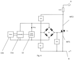
- FIG. 3 an embodiment of the invention is shown which is a power supply circuit for controlling how AC power (such as mains power) connected to points A and B delivered to a load.
- the power supply circuit includes a triac T1 having a control input (gate) G and power terminals MT1 and MT2.
- On/off control of the triac T1 is done by a controller 11 (typically a microcontroller), for generating a control signal for controlling the triac T1.
- the control signal is typically a (negative) current pulse.
- the controller 11 is coupled to the gate G of the triac T1 via a rectifier B1 and, optionally, other circuits.
- the control signal generated by the controller 11 is used to control a gate driver circuit 14 connected across the two outputs O1, O2 of the bridge B1.
- the gate driver circuit 14 amplifies the voltage pulse and a current Itrig passes through it.
- the gate driver simply produces a digital form of the output from the controller 11.
- the controller 11 is powered by a power supply 10 via a power line 14.
- the power supply 10 draws its power from the output of the rectifier B1.
- the power supply unit 10 receives power once per half cycle, and only when the triac T1 is not conducting. It is typically designed to keep the controller operating from half-cycle to half-cycle, so that longer duration control is possible.
- the power supply 10 is not exposed to mains voltage, so it can be designed in a very simple, compact and low cost way, i.e. it can be significantly simpler than the power supply unit of Fig. 1 . At a minimum it is simply a capacitor for storing charge to keep the controller running to perform its function of generating the control signal.
- the power supply 10 also has a voltage regulation function.
- the power supply 10 also has a function of controlling the timing with which the controller 11 generates the control signal.
- the controller 11 may be controlled based on the timing of the mains supply.
- an optional signal line 13 may be provided from the power supply 10 to the controller 11, and a detection circuit may be provided associated with the power supply 10 and operative to detect the rise of current or voltage from the rectifier into the power supply 10, and accordingly transmit a timing signal on the signal line 13 to the controller 11.
- the rise in the current or voltage from the rectifier into the power supply 10 indicates a rise of the magnitude (irrespective of the sign) of the voltage across the triac.
- the controller would be enabled to generate the control signal with a timing based on the timing of the AC signal (e.g. synchronised with certain points on the AC waveform), or the controller may count mains cycles and have a timing based on that.
- controller 11 will be provided as a single integrated circuit (IC), which may include other functions such as regulation.
- IC integrated circuit
- the construction of the controller 11 and the gate driver circuit 12 will be well-known to a person skilled in the art. It may for example involve the use of components as described in document AN467 "NXP's 51 LPC-Microcontrollers and Triacs easily constructed", published by NXP BV (2013 ).
- the power supply circuit further comprises impedances ZH, ZL and ZG.
- ZH and ZL have a capacitive component, and constitute a capacitive network in parallel with the triac.
- a first input I1 of the rectifier B1 is electrically connected to ZH and ZL, while the second input I2 of the rectifier B1 is connected to the gate G of the triac T1.
- Fig. 1 B1 is shown as a bridge rectifier, which is preferable, however other rectifier configurations are possible.
- the rectifier is a full-wave rectifier.
- the rectifier could be a half wave rectifier; the power supply 10 would in this case only be powered in every other half-cycle, and would be typically designed to store enough power the controller 10 for the full AC period.
- the controller 11 When the controller 11 generates a control signal, it is amplified by the gate driver circuit 14, the amplified control signal is transmitted by the rectifier B1 to the gate (G) of the triac T1.
- Current for the pulses is provided from the capacitive network ZL and ZH, from AC power conducted via the load.
- ZL and ZH may have complex characteristics provided they are capacitive, preferably mainly capacitive. However, it is possible to form an embodiment in which ZL is resistive with only ZH being capacitive.
- the triac T1 is turned off and the AC voltage increases then the voltage across MT2 - MT1 also increases. This increases the voltage across ZL, and stores energy in its capacitive characteristic.
- the voltage across ZL also passes via the rectifier B1 to the power supply 10 for the controller 11 to power it.
- the power supply 10 may include capacitive energy storage to maintain supply voltage to the controller when there is no (or low) voltage across ZL. In applications where the controller needs to maintain function over a period longer than half of the AC cycle, the controller power supply would need to store sufficient energy to maintain operation from one non-conduction period of the triac to the next non-conduction period, when the energy can be recharged.
- ZH does not include a significant current path which bypasses the capacitive elements of ZH.
- ZH is substantially capacitive.
- Using a substantially capacitive impedance for ZH allows very low power consumption when the triac is held in the off-state (i.e. not triggered, with no power going to the load). This is significant for an application in which the embodiment controls a refrigerator because the off-state power has to be very low, and this arrangement is a particularly cost effective way to achieve it.
- Other applications e.g. controlling lights or a thermostat also benefit from similar low off-state power consumption
- Recharge of the controller power supply 10 requires current flow through the rectifier B1, and this current will also flow to the gate node G of the triac T1. There is a possibility that this current could trigger the triac T1 prematurely, simply due to recharge of the power supply.
- one or more circuits can be included to reduce the charging current (for example by including a series resistance or a current limiting circuit) and/or reduce the sensitivity of the gate node to current (for example bypassing some current through bypass impedance ZG to MT1).
- a further purpose of the optional bypass impedance ZG is to improve the commutation performance of the triac.
- the total charge transmitted from the gate driver circuit 12 to trigger the triac T1 cannot exceed the total charge transmitted from ZH and ZL to the controller power supply 10.
- the gate driver current (Itrig) is concentrated into short duration current pulses of amplitude sufficient to trigger the triac T1 reliably.
- the current charging the power supply 10 is allowed to pass over a significantly longer period, at low amplitude.
- the trigger current pulse is very short.
- the controller 11 may be arranged initially to generate a very short current pulse but detect when triggering has failed by sensing the rise of voltage to the power supply; if the controller 11 issues a trigger but the power supply input voltage (i.e. the output of the rectifier B1) is seen to subsequently rise then the controller may subsequently issue another triggering pulse (either at once or a short time later). This could for example be during the same half-cycle, but at a time when the mains voltage has risen further in the mains cycle so that the triggering could be more reliable even if the triggering pulse is the same.
- the controller 10 may be operative to detect that the triggering pulses are not reliably triggering the triac T1, and start to generate a longer or larger current pulse to provide more effective triggering.
- Fig. 3 can be varied in a number of ways within the scope of the invention.
- the single rectifier B1 can be replaced in other embodiments with two separate rectifiers.
- One rectifier would have the function of transmitting the control signal from the controller 11 to the gate G of the triac T1.
- the other rectifier would have the function of generating power for the power supply unit 10.
- the use of a single rectifier B1 to perform both these functions is preferred.
- the power supply circuit may operate the triac T1 with the opposite polarity.
- the gate trigger current is provided from either of the impedances ZL, ZH or both.
- the capacitive network would omit the impedance ZL, relying only on charge from ZH.
- a further advantage of using a capacitive impedance for ZH is that high voltage impulses, typical of surge conditions, can be arranged to pass through ZH and be conducted to the gate terminal G of the triac T1 making it trigger. In some applications this is very beneficial because it protects the triac T1 from overvoltage conditions. It does, however, turn on the triac T1 which will conduct for some part of the mains cycle, hence powering the load briefly. There are some applications where this would not be acceptable but others where it would be, for example: motor-compressor control in refrigeration, heaters, and some lighting applications. Protective behaviour of this form allows the use of low-cost components while resisting high values of surge voltage. Alternative methods to protect against surges often require expensive additional protection devices.
- the power supply 10 ensures that the controller remains powered continuously while mains supply power is applied (whether or not power is supplied to the load). This is important since it is necessary to keep "state" information from one half-cycle of the supply to the next.
- the state information includes, typically:
- both the accumulator and the expired state are reset. Only while the expired state remains in the reset state, power is supplied to the load.
- the accumulator is increased at a rate, at least during the on-time.
- the expired state is set, therefore preventing further application of power to the load until the system is reset by removal and re-application of power.
- a digital embodiment of the controller 11 could use a counter as the accumulator, incrementing with time or mains half-cycles, and a logical bit to hold the expired state.
- a counter as the accumulator, incrementing with time or mains half-cycles, and a logical bit to hold the expired state.
- other embodiments are possible, for example forming the controller 11 using discrete components and/or using analogue rather than digital circuit techniques. The other embodiments would still provide the necessary functions and, in particular, for a timing application, maintain the accumulator and expired states. They are maintained even when power is not instantaneously available to the controller via the rectifier.
- the second embodiment differs from the first embodiment of Fig. 3 only in the arrangement of the controller, and the omission of the power supply unit 10.
- the second embodiment includes a controller in two portions: a controller portion 11a with power applied only intermittently from the rectifier and a store 11b that may comprise one or more storage elements.
- the store 11b holds a time accumulator and an expired state in one or more elements.
- Other, more complex control implementations may have storage elements to hold (or represent) other states or conditions.
- a capacitor can be used as a time accumulator; charge being added (or removed) at least during the on-time. Its voltage then represents the elapsed time and when it reaches a threshold then the on-time can be determined to have expired.
- the expired state can be represented by the voltage/charge in a separate capacitor, with high charge representing the expired state.
- a single capacitor can be used to provide both the accumulation and expired states:
- charge may be added or removed from the capacitor during the on-time, and the expiration can be determined by the voltage rising above or falling below a threshold.
- the DC voltage output from the rectifier to the controller portion 11a is related to the applied mains voltage and the ratios of impedances in the network feeding the rectifier from the mains supply, but mainly the ratio of CH to CL. If the mains supply is completely removed, then no voltage will be provided by the rectifier. In this circumstance, capacitors used as store element(s) can be reset simply by draining their charge through some high value resistance. In many applications this gives acceptable performance. In some applications, however, there can be a residual voltage at the mains supply in the condition when the supply is nominally off. In these circumstances there would be a voltage output from the rectifier.
- a scheme such as described can be implemented as a simple analogue circuit using low cost devices, either discrete or integrated. Note also that the gate driver function may also be integrated into the circuit of the controller portion 11a, rather than being provided as additional circuits.
- Fig. 5 shows a third embodiment the invention.
- the power supply 10, controller, and gate driver circuit 12 are as in the first embodiment of Fig. 3 or as in the second embodiment of Fig. 4 , and are omitted for simplicity.
- the second embodiment also includes the circuits ZH, ZL and ZG, and Fig. 5 shows a specific form these might take in either embodiment: in Fig. 5 , ZH comprises a capacitor CH, and resistors RH1 and RH2; ZL comprises a capacitor CL; and ZG comprises a resistor RG. Forming ZH with one or more capacitive elements in series with one or more resistive ones avoids excessive current passing through ZH and ZL under transient conditions.
- the third embodiment differs from the first or second in that an additional surge current circuit X1 is provided, which is arranged to pass current whenever a surge pulse is applied via the AC power connections.
- X1 could be a capacitor, a bidirectional transient voltage suppressor (TVS) device or a more complicated circuit.
- the required characteristic of X1 is to pass gate trigger current when high levels of current flow through CH - characteristic of surge conditions applied via the mains connections.
- a capacitor as X1 fast application of high current through CH preferentially passes through X1 to the gate G of the triac T1.
- a further method of triggering the triac under surge conditions is to limit the voltage across the rectified output of the rectifier B1 using a device such as a zener diode or other means.
- a device such as a zener diode or other means.
- FIG. 6 A fourth embodiment, which facilitates improve setting of behaviour under surge conditions is illustrated in Fig. 6 . Again, this is a variant of the first or second embodiment, and elements of those embodiments which are the same in the fourth embodiment are omitted in Fig. 6 . Note that in the fourth embodiment, as compared to the third embodiment, RH1 is repositioned in relation to the rectifier and that over-voltage protection device X2 is added, X1 having been removed.
- a fast over-voltage event such as a surge
- the output voltage from the rectifier (applied to X2) rises as a proportion of applied voltage, related to the ratio of resistances RH1 to RH2 (the load impedance generally being low in comparison).
- X2 is a device that conducts current appreciably only when a threshold voltage is exceeded (e.g.
- the rectifier will conduct current once the applied overvoltage exceeds a threshold that can be determined mainly by the X2 threshold and the ratio RH1 to RH2.
- a threshold that can be determined mainly by the X2 threshold and the ratio RH1 to RH2.
- the corresponding current flows to the triac gate which is then arranged to trigger. Triggering the triac prevents it being subjected to excessive overvoltage.
- X2 Under normal operating conditions (without applied overvoltage), X2 need not interfere with circuit function or can be used for some other function if desired.
- the overvoltage characteristic can be provided by a behaviour of the controller circuit itself, rather than being provided by an additional device (X2).
- the value of RH1 must be taken into account in relation to passage of trigger current to the gate of the triac but it is practical to choose a suitable value that also allows acceptable overvoltage protection behaviour.
- Forming ZL with one or more series resistive elements allows surge-protection behaviour (similarly to how X1 provides it in the third embodiment).
- Such an implementation may reduce the cost of the overall circuit, since it avoids using a bidirectional overvoltage device (X1), which is typically more expensive than a zener diode. Further, if the overvoltage characteristic is provided by a controller behaviour, or the device X2 is used also within a controller function, then there is an overall cost saving.
- the controller 11 or 11a of the embodiments of Figs. 3 to 6 are powered via rectifier B1 from the gate circuit of the triac, and the zero-voltage reference of the controller is not connected to the MT1 terminal of the triac T1, as is conventional in controller/triac combinations. If the controller 11 or 11a requires no additional connections in the application system then this is not a hindrance.
- An example of such a supply circuit system is a timing system in which the controller 11 or 11a turns the triac T1 on and off at predetermined periods after the first application of power.
- other applications may require the controller 11 or 11a to be connected to other circuits; for example, in the case that the power supply is used as a thermostat controlled by a remote sensor.
- these other circuits would have no current path to the AC supply connections.
- Fig. 7 Such an embodiment is shown in Fig. 7 , which differs from the embodiment of Fig. 3 only in that an sensor 15 is provided (e.g. remote from the controller 11) to control the controller 11.
- an sensor 15 e.g. remote from the controller 11
- the remote sensor 15 may be replaced by another form of control circuit.
- Fig. 5 shows the signal line 14 of Fig. 3 being present, such that the control of the controller 11 may be based on both the timing of the AC circuit and the output of the sensor 15, the signal line 14 may optionally be omitted.
- the controller preferably receives a signal derived from the voltage or current from the rectifier to synchronise operation to the mains cycle and/or to count mains cycles.
Landscapes
- Engineering & Computer Science (AREA)
- Power Engineering (AREA)
- Power Conversion In General (AREA)
- Control Of Electrical Variables (AREA)
Claims (8)
- Stromversorgungsschaltung zum Steuern der Zufuhr von Strom von einer Stromquelle für Wechselstrom, AC, zu einer Last, wobei die Stromversorgungsschaltung Folgendes umfasst:eine Triac-Einheit (T1) zur Anordnung in Reihe mit der Last, wobei die Triac-Einheit (T1) einen Steuerungseingang (G), einen MT1-Anschluss und einen MT2-Anschluss aufweist;eine Steuerungseinrichtung (11; 11a, 11b), die betriebsfähig ist, um ein Steuerungssignal zu erzeugen, wobei die Steuerungseinrichtung (11; 11a) betriebsfähig ist, um die Triac-Einheit (T1) unter Verwendung des Steuerungssignals zu zünden;eine Gleichrichtereinheit, die mindestens einen Gleichrichter (B1) umfasst; undein kapazitives Netzwerk (ZL, ZH), wobei ein Anschluss des kapazitiven Netzwerks mit einem Eingang (I1) der Gleichrichtereinheit elektrisch verbunden ist,wobei die Gleichrichtereinheit betriebsfähig zwischen die Steuerungseinrichtung (11; 11a, 11b) und den Steuerungseingang (G) der Triac-Einheit (T1) geschaltet ist, und betriebsfähig ist, um:(i) das Steuerungssignal von der Steuerungseinrichtung (11; 11a, 11b) zum Steuerungseingang (G) der Triac-Einheit (T1) zu leiten, um die Triac-Einheit (T1) unter Verwendung des Steuerungssignals zu zünden, und(ii) elektrischen Strom zur Steuerungseinrichtung (11; 11a, 11b) zu übertragen,wobei die Stromversorgungsschaltung dadurch gekennzeichnet ist, dass:
das kapazitive Netzwerk (ZL, ZH) eine kapazitive Schaltung (ZH) mit einem ersten und einem zweiten Anschluss einschließt, wobei der erste Anschluss mit dem Eingang (11) der Gleichrichtereinheit verbunden ist, und der zweite Anschluss mit dem MT2-Anschluss der Triac-Einheit (T1) verbunden ist. - Stromversorgungsschaltung nach Anspruch 1, ferner eine Stromversorgungseinheit (10) umfassend, wobei das Steuerungssignal in Form eines Stromimpulses mit einer Dauer, die kürzer als eine Ladeperiode der Stromversorgungseinheit (10) ist, zum Steuerungseingang (G) der Triac-Einheit (T1) geleitet wird.
- Stromversorgungsschaltung nach Anspruch 1, bei der die Steuerungseinrichtung (11a, 11b) einen Kondensator zum Speichern einer Ladung einschließt, wobei die Steuerungseinrichtung betriebsfähig ist, um das Steuerungssignal in Abhängigkeit von der gespeicherten Ladung zu erzeugen.
- Stromversorgung nach einem der vorhergehenden Ansprüche, ferner eine Stromüberbrückungsschaltung (ZG) einschließend, die zwischen den Steuerungseingang (G) der Triac-Einheit (T1) und den MT1-Anschluss der Triac-Einheit (T1) geschaltet ist.
- Stromversorgungsschaltung nach einem der vorhergehenden Ansprüche, ferner eine Spitzenstromschaltung (X1; X2) einschließend, die betriebsfähig ist, um, falls dem Strom von der Stromquelle für Wechselstrom, AC, eine Stromspitze überlagert ist, ein Zündsignal zum Steuerungseingang (G) zu übertragen, um die Triac-Einheit (T1) zu zünden, wobei die Spitzenstromschaltung (X2) vorzugsweise zwischen Ausgänge (O1, O2) des Gleichrichters (B1) geschaltet ist.
- Stromversorgungsschaltung nach einem der vorhergehenden Ansprüche, ferner einen Sensor (15) umfassend, der betriebsfähig ist, um ein Merkmal der Umgebung des Sensors zu erfassen, wobei er unter Verwendung des erfassten Merkmals ein Eingangssignal erzeugt, und um das Eingangssignal zur Steuerungseinrichtung zu übertragen, wobei die Steuerungseinrichtung betriebsfähig ist, um das Steuerungssignal in Abhängigkeit von dem Eingangssignal zu erzeugen.
- Stromversorgungsschaltung nach einem der vorhergehenden Ansprüche,
wobei die Steuerungseinrichtung (11; 11a, 11b) betriebsfähig ist, um zu ermitteln, ob das Steuerungssignal die Triac-Einheit (T1) gezündet hat, und falls die Bestimmung negativ ist, um ein weiteres Steuerungssignal zu übertragen, um die Triac-Einheit (T1) zu zünden. - Stromversorgung nach einem der vorhergehenden Ansprüche, eine Schaltung umfassend, die betriebsfähig ist, um einen ansteigenden Strom oder eine ansteigende Spannung in dem Steuerungssignal zu ermitteln, das durch die Gleichrichtereinheit zum Steuerungseingang (G) der Triac-Einheit (T1) geleitet wird, und dementsprechend die Zeitgebung zu steuern, mit der die Steuerungseinrichtung (11; 11a, 11b) das Steuerungssignal erzeugt.
Applications Claiming Priority (2)
| Application Number | Priority Date | Filing Date | Title |
|---|---|---|---|
| GBGB1515569.0A GB201515569D0 (en) | 2015-09-02 | 2015-09-02 | Triac control system |
| GB1521526.2A GB2541958B (en) | 2015-09-02 | 2015-12-07 | Triac control systems |
Publications (3)
| Publication Number | Publication Date |
|---|---|
| EP3139708A2 EP3139708A2 (de) | 2017-03-08 |
| EP3139708A3 EP3139708A3 (de) | 2017-06-21 |
| EP3139708B1 true EP3139708B1 (de) | 2023-06-21 |
Family
ID=54326690
Family Applications (1)
| Application Number | Title | Priority Date | Filing Date |
|---|---|---|---|
| EP16185910.3A Active EP3139708B1 (de) | 2015-09-02 | 2016-08-26 | Triac-steuerungssysteme |
Country Status (3)
| Country | Link |
|---|---|
| EP (1) | EP3139708B1 (de) |
| GB (2) | GB201515569D0 (de) |
| PL (1) | PL3139708T3 (de) |
Families Citing this family (1)
| Publication number | Priority date | Publication date | Assignee | Title |
|---|---|---|---|---|
| CN108512535B (zh) * | 2018-03-29 | 2022-01-18 | 华南理工大学 | 采用正温度系数热敏电阻补偿的可控硅触发电路 |
Citations (1)
| Publication number | Priority date | Publication date | Assignee | Title |
|---|---|---|---|---|
| EP1052776A2 (de) * | 1999-04-22 | 2000-11-15 | Zhongdu Liu | Elektrischer Halbleiterschalter |
Family Cites Families (5)
| Publication number | Priority date | Publication date | Assignee | Title |
|---|---|---|---|---|
| US4878010A (en) * | 1987-12-10 | 1989-10-31 | Weber Harold J | Electric a.c power switch controller and d.c. power supply method and apparatus |
| GB2330704A (en) * | 1997-10-21 | 1999-04-28 | Timeguard Limited | Semiconductor AC switch units |
| US6388345B1 (en) * | 2000-05-01 | 2002-05-14 | Aaron N. Stimpson | Corner light switch assembly |
| JP2004343561A (ja) * | 2003-05-16 | 2004-12-02 | Matsushita Electric Works Ltd | 照度センサスイッチ |
| DE102006016392A1 (de) * | 2005-12-17 | 2007-06-21 | Abb Patent Gmbh | Elektronikschaltung zum Schalten/Dimmen von Wechselströmen unter Einsatz eines Triacs |
-
2015
- 2015-09-02 GB GBGB1515569.0A patent/GB201515569D0/en not_active Ceased
- 2015-12-07 GB GB1521526.2A patent/GB2541958B/en active Active
-
2016
- 2016-08-26 EP EP16185910.3A patent/EP3139708B1/de active Active
- 2016-08-26 PL PL16185910.3T patent/PL3139708T3/pl unknown
Patent Citations (1)
| Publication number | Priority date | Publication date | Assignee | Title |
|---|---|---|---|---|
| EP1052776A2 (de) * | 1999-04-22 | 2000-11-15 | Zhongdu Liu | Elektrischer Halbleiterschalter |
Also Published As
| Publication number | Publication date |
|---|---|
| EP3139708A3 (de) | 2017-06-21 |
| GB2541958A (en) | 2017-03-08 |
| PL3139708T3 (pl) | 2023-12-04 |
| GB201521526D0 (en) | 2016-01-20 |
| EP3139708A2 (de) | 2017-03-08 |
| GB2541958B (en) | 2017-12-13 |
| GB201515569D0 (en) | 2015-10-14 |
Similar Documents
| Publication | Publication Date | Title |
|---|---|---|
| US9620991B2 (en) | Power stealing circuitry for a control device | |
| US8928235B2 (en) | Damper circuit for switched dimming | |
| JP6430496B2 (ja) | 非線形軽負荷の調光器用のブリーダ回路 | |
| JP5314413B2 (ja) | 負荷制御装置 | |
| US20150116874A1 (en) | Overvoltage protection circuit | |
| WO2020068089A1 (en) | Dimmer with improved noise immunity | |
| EP3319401B1 (de) | Dimmvorrichtung | |
| JP2016025456A (ja) | スイッチ装置及びそれを用いた負荷制御システム | |
| US9992849B1 (en) | Overvoltage detection in a dimmer | |
| RU2661311C2 (ru) | Электронная схема и способ работы электронной схемы | |
| US9391536B2 (en) | Method for providing low voltage DC power from AC mains power | |
| EP3139708B1 (de) | Triac-steuerungssysteme | |
| TWI631875B (zh) | 調光裝置之保護電路及調光裝置 | |
| TWI618451B (zh) | 保護電路及配線器具 | |
| US20030161082A1 (en) | Power supply with low los making current limitation | |
| JP6481925B2 (ja) | スイッチ装置 | |
| WO1983004458A1 (en) | Proximity switch circuit | |
| JP2007174575A (ja) | 2線式電子スイッチ | |
| US8994283B2 (en) | Circuit for controlling a lighting unit having a periodic power supply with a thyristor | |
| JP2011258431A (ja) | 電源回路及び照明装置及び照明システム | |
| US20230100378A1 (en) | Switching control circuits and method of actuating a switch having reduced conducted emi | |
| JP4552850B2 (ja) | 2線式電子スイッチ | |
| JP2019207833A (ja) | 照明用電源装置 | |
| US11677235B2 (en) | Avalanche triggered overvoltage protection | |
| JP2004266970A (ja) | 整流切換回路 |
Legal Events
| Date | Code | Title | Description |
|---|---|---|---|
| PUAI | Public reference made under article 153(3) epc to a published international application that has entered the european phase |
Free format text: ORIGINAL CODE: 0009012 |
|
| STAA | Information on the status of an ep patent application or granted ep patent |
Free format text: STATUS: THE APPLICATION HAS BEEN PUBLISHED |
|
| AK | Designated contracting states |
Kind code of ref document: A2 Designated state(s): AL AT BE BG CH CY CZ DE DK EE ES FI FR GB GR HR HU IE IS IT LI LT LU LV MC MK MT NL NO PL PT RO RS SE SI SK SM TR |
|
| AX | Request for extension of the european patent |
Extension state: BA ME |
|
| RIC1 | Information provided on ipc code assigned before grant |
Ipc: H02M 1/00 20070101ALI20170209BHEP Ipc: H05B 39/08 20060101ALI20170209BHEP Ipc: H05B 37/02 20060101AFI20170209BHEP Ipc: H05B 1/02 20060101ALI20170209BHEP Ipc: H02M 5/257 20060101ALI20170209BHEP Ipc: G05D 25/02 20060101ALI20170209BHEP |
|
| PUAL | Search report despatched |
Free format text: ORIGINAL CODE: 0009013 |
|
| AK | Designated contracting states |
Kind code of ref document: A3 Designated state(s): AL AT BE BG CH CY CZ DE DK EE ES FI FR GB GR HR HU IE IS IT LI LT LU LV MC MK MT NL NO PL PT RO RS SE SI SK SM TR |
|
| AX | Request for extension of the european patent |
Extension state: BA ME |
|
| RIC1 | Information provided on ipc code assigned before grant |
Ipc: H02M 5/257 20060101ALI20170512BHEP Ipc: G05D 25/02 20060101ALI20170512BHEP Ipc: H05B 37/02 20060101AFI20170512BHEP Ipc: H05B 1/02 20060101ALI20170512BHEP Ipc: H05B 39/08 20060101ALI20170512BHEP Ipc: H02M 1/00 20070101ALI20170512BHEP |
|
| STAA | Information on the status of an ep patent application or granted ep patent |
Free format text: STATUS: REQUEST FOR EXAMINATION WAS MADE |
|
| 17P | Request for examination filed |
Effective date: 20170616 |
|
| STAA | Information on the status of an ep patent application or granted ep patent |
Free format text: STATUS: EXAMINATION IS IN PROGRESS |
|
| 17Q | First examination report despatched |
Effective date: 20200324 |
|
| STAA | Information on the status of an ep patent application or granted ep patent |
Free format text: STATUS: EXAMINATION IS IN PROGRESS |
|
| REG | Reference to a national code |
Ref country code: DE Ref legal event code: R079 Ref document number: 602016080435 Country of ref document: DE Free format text: PREVIOUS MAIN CLASS: H05B0037020000 Ipc: H05B0039080000 |
|
| GRAP | Despatch of communication of intention to grant a patent |
Free format text: ORIGINAL CODE: EPIDOSNIGR1 |
|
| STAA | Information on the status of an ep patent application or granted ep patent |
Free format text: STATUS: GRANT OF PATENT IS INTENDED |
|
| RIC1 | Information provided on ipc code assigned before grant |
Ipc: H05B 47/10 20200101ALI20221130BHEP Ipc: H05B 1/02 20060101ALI20221130BHEP Ipc: H03K 17/725 20060101ALI20221130BHEP Ipc: H02P 27/02 20160101ALI20221130BHEP Ipc: H05B 39/08 20060101AFI20221130BHEP |
|
| INTG | Intention to grant announced |
Effective date: 20230103 |
|
| GRAS | Grant fee paid |
Free format text: ORIGINAL CODE: EPIDOSNIGR3 |
|
| GRAA | (expected) grant |
Free format text: ORIGINAL CODE: 0009210 |
|
| STAA | Information on the status of an ep patent application or granted ep patent |
Free format text: STATUS: THE PATENT HAS BEEN GRANTED |
|
| AK | Designated contracting states |
Kind code of ref document: B1 Designated state(s): AL AT BE BG CH CY CZ DE DK EE ES FI FR GB GR HR HU IE IS IT LI LT LU LV MC MK MT NL NO PL PT RO RS SE SI SK SM TR |
|
| REG | Reference to a national code |
Ref country code: CH Ref legal event code: EP |
|
| REG | Reference to a national code |
Ref country code: DE Ref legal event code: R096 Ref document number: 602016080435 Country of ref document: DE |
|
| REG | Reference to a national code |
Ref country code: AT Ref legal event code: REF Ref document number: 1581848 Country of ref document: AT Kind code of ref document: T Effective date: 20230715 |
|
| REG | Reference to a national code |
Ref country code: IE Ref legal event code: FG4D |
|
| REG | Reference to a national code |
Ref country code: LT Ref legal event code: MG9D |
|
| REG | Reference to a national code |
Ref country code: NL Ref legal event code: MP Effective date: 20230621 |
|
| PG25 | Lapsed in a contracting state [announced via postgrant information from national office to epo] |
Ref country code: SE Free format text: LAPSE BECAUSE OF FAILURE TO SUBMIT A TRANSLATION OF THE DESCRIPTION OR TO PAY THE FEE WITHIN THE PRESCRIBED TIME-LIMIT Effective date: 20230621 Ref country code: NO Free format text: LAPSE BECAUSE OF FAILURE TO SUBMIT A TRANSLATION OF THE DESCRIPTION OR TO PAY THE FEE WITHIN THE PRESCRIBED TIME-LIMIT Effective date: 20230921 |
|
| PGFP | Annual fee paid to national office [announced via postgrant information from national office to epo] |
Ref country code: GB Payment date: 20230928 Year of fee payment: 8 |
|
| REG | Reference to a national code |
Ref country code: AT Ref legal event code: MK05 Ref document number: 1581848 Country of ref document: AT Kind code of ref document: T Effective date: 20230621 |
|
| PG25 | Lapsed in a contracting state [announced via postgrant information from national office to epo] |
Ref country code: RS Free format text: LAPSE BECAUSE OF FAILURE TO SUBMIT A TRANSLATION OF THE DESCRIPTION OR TO PAY THE FEE WITHIN THE PRESCRIBED TIME-LIMIT Effective date: 20230621 Ref country code: NL Free format text: LAPSE BECAUSE OF FAILURE TO SUBMIT A TRANSLATION OF THE DESCRIPTION OR TO PAY THE FEE WITHIN THE PRESCRIBED TIME-LIMIT Effective date: 20230621 Ref country code: LV Free format text: LAPSE BECAUSE OF FAILURE TO SUBMIT A TRANSLATION OF THE DESCRIPTION OR TO PAY THE FEE WITHIN THE PRESCRIBED TIME-LIMIT Effective date: 20230621 Ref country code: LT Free format text: LAPSE BECAUSE OF FAILURE TO SUBMIT A TRANSLATION OF THE DESCRIPTION OR TO PAY THE FEE WITHIN THE PRESCRIBED TIME-LIMIT Effective date: 20230621 Ref country code: HR Free format text: LAPSE BECAUSE OF FAILURE TO SUBMIT A TRANSLATION OF THE DESCRIPTION OR TO PAY THE FEE WITHIN THE PRESCRIBED TIME-LIMIT Effective date: 20230621 Ref country code: GR Free format text: LAPSE BECAUSE OF FAILURE TO SUBMIT A TRANSLATION OF THE DESCRIPTION OR TO PAY THE FEE WITHIN THE PRESCRIBED TIME-LIMIT Effective date: 20230922 |
|
| PGFP | Annual fee paid to national office [announced via postgrant information from national office to epo] |
Ref country code: FR Payment date: 20230929 Year of fee payment: 8 Ref country code: DE Payment date: 20230929 Year of fee payment: 8 |
|
| PG25 | Lapsed in a contracting state [announced via postgrant information from national office to epo] |
Ref country code: FI Free format text: LAPSE BECAUSE OF FAILURE TO SUBMIT A TRANSLATION OF THE DESCRIPTION OR TO PAY THE FEE WITHIN THE PRESCRIBED TIME-LIMIT Effective date: 20230621 |
|
| PG25 | Lapsed in a contracting state [announced via postgrant information from national office to epo] |
Ref country code: SK Free format text: LAPSE BECAUSE OF FAILURE TO SUBMIT A TRANSLATION OF THE DESCRIPTION OR TO PAY THE FEE WITHIN THE PRESCRIBED TIME-LIMIT Effective date: 20230621 |
|
| PG25 | Lapsed in a contracting state [announced via postgrant information from national office to epo] |
Ref country code: ES Free format text: LAPSE BECAUSE OF FAILURE TO SUBMIT A TRANSLATION OF THE DESCRIPTION OR TO PAY THE FEE WITHIN THE PRESCRIBED TIME-LIMIT Effective date: 20230621 |
|
| PG25 | Lapsed in a contracting state [announced via postgrant information from national office to epo] |
Ref country code: IS Free format text: LAPSE BECAUSE OF FAILURE TO SUBMIT A TRANSLATION OF THE DESCRIPTION OR TO PAY THE FEE WITHIN THE PRESCRIBED TIME-LIMIT Effective date: 20231021 |
|
| PG25 | Lapsed in a contracting state [announced via postgrant information from national office to epo] |
Ref country code: SM Free format text: LAPSE BECAUSE OF FAILURE TO SUBMIT A TRANSLATION OF THE DESCRIPTION OR TO PAY THE FEE WITHIN THE PRESCRIBED TIME-LIMIT Effective date: 20230621 Ref country code: SK Free format text: LAPSE BECAUSE OF FAILURE TO SUBMIT A TRANSLATION OF THE DESCRIPTION OR TO PAY THE FEE WITHIN THE PRESCRIBED TIME-LIMIT Effective date: 20230621 Ref country code: RO Free format text: LAPSE BECAUSE OF FAILURE TO SUBMIT A TRANSLATION OF THE DESCRIPTION OR TO PAY THE FEE WITHIN THE PRESCRIBED TIME-LIMIT Effective date: 20230621 Ref country code: PT Free format text: LAPSE BECAUSE OF FAILURE TO SUBMIT A TRANSLATION OF THE DESCRIPTION OR TO PAY THE FEE WITHIN THE PRESCRIBED TIME-LIMIT Effective date: 20231023 Ref country code: IS Free format text: LAPSE BECAUSE OF FAILURE TO SUBMIT A TRANSLATION OF THE DESCRIPTION OR TO PAY THE FEE WITHIN THE PRESCRIBED TIME-LIMIT Effective date: 20231021 Ref country code: ES Free format text: LAPSE BECAUSE OF FAILURE TO SUBMIT A TRANSLATION OF THE DESCRIPTION OR TO PAY THE FEE WITHIN THE PRESCRIBED TIME-LIMIT Effective date: 20230621 Ref country code: EE Free format text: LAPSE BECAUSE OF FAILURE TO SUBMIT A TRANSLATION OF THE DESCRIPTION OR TO PAY THE FEE WITHIN THE PRESCRIBED TIME-LIMIT Effective date: 20230621 Ref country code: CZ Free format text: LAPSE BECAUSE OF FAILURE TO SUBMIT A TRANSLATION OF THE DESCRIPTION OR TO PAY THE FEE WITHIN THE PRESCRIBED TIME-LIMIT Effective date: 20230621 Ref country code: AT Free format text: LAPSE BECAUSE OF FAILURE TO SUBMIT A TRANSLATION OF THE DESCRIPTION OR TO PAY THE FEE WITHIN THE PRESCRIBED TIME-LIMIT Effective date: 20230621 |
|
| PGFP | Annual fee paid to national office [announced via postgrant information from national office to epo] |
Ref country code: TR Payment date: 20231017 Year of fee payment: 8 Ref country code: IT Payment date: 20231010 Year of fee payment: 8 |
|
| PGFP | Annual fee paid to national office [announced via postgrant information from national office to epo] |
Ref country code: PL Payment date: 20231012 Year of fee payment: 8 |
|
| PG25 | Lapsed in a contracting state [announced via postgrant information from national office to epo] |
Ref country code: MC Free format text: LAPSE BECAUSE OF FAILURE TO SUBMIT A TRANSLATION OF THE DESCRIPTION OR TO PAY THE FEE WITHIN THE PRESCRIBED TIME-LIMIT Effective date: 20230621 |
|
| REG | Reference to a national code |
Ref country code: DE Ref legal event code: R097 Ref document number: 602016080435 Country of ref document: DE |
|
| REG | Reference to a national code |
Ref country code: CH Ref legal event code: PL |
|
| PG25 | Lapsed in a contracting state [announced via postgrant information from national office to epo] |
Ref country code: MC Free format text: LAPSE BECAUSE OF FAILURE TO SUBMIT A TRANSLATION OF THE DESCRIPTION OR TO PAY THE FEE WITHIN THE PRESCRIBED TIME-LIMIT Effective date: 20230621 |
|
| PG25 | Lapsed in a contracting state [announced via postgrant information from national office to epo] |
Ref country code: LU Free format text: LAPSE BECAUSE OF NON-PAYMENT OF DUE FEES Effective date: 20230826 |
|
| PLBE | No opposition filed within time limit |
Free format text: ORIGINAL CODE: 0009261 |
|
| STAA | Information on the status of an ep patent application or granted ep patent |
Free format text: STATUS: NO OPPOSITION FILED WITHIN TIME LIMIT |
|
| PG25 | Lapsed in a contracting state [announced via postgrant information from national office to epo] |
Ref country code: LU Free format text: LAPSE BECAUSE OF NON-PAYMENT OF DUE FEES Effective date: 20230826 Ref country code: DK Free format text: LAPSE BECAUSE OF FAILURE TO SUBMIT A TRANSLATION OF THE DESCRIPTION OR TO PAY THE FEE WITHIN THE PRESCRIBED TIME-LIMIT Effective date: 20230621 Ref country code: CH Free format text: LAPSE BECAUSE OF NON-PAYMENT OF DUE FEES Effective date: 20230831 |
|
| PG25 | Lapsed in a contracting state [announced via postgrant information from national office to epo] |
Ref country code: SI Free format text: LAPSE BECAUSE OF FAILURE TO SUBMIT A TRANSLATION OF THE DESCRIPTION OR TO PAY THE FEE WITHIN THE PRESCRIBED TIME-LIMIT Effective date: 20230621 |
|
| REG | Reference to a national code |
Ref country code: BE Ref legal event code: MM Effective date: 20230831 |
|
| REG | Reference to a national code |
Ref country code: IE Ref legal event code: MM4A |